WO2012157208A1 - プラスチックフィルム、表示装置及びマルチディスプレイ装置 - Google Patents
プラスチックフィルム、表示装置及びマルチディスプレイ装置 Download PDFInfo
- Publication number
- WO2012157208A1 WO2012157208A1 PCT/JP2012/003026 JP2012003026W WO2012157208A1 WO 2012157208 A1 WO2012157208 A1 WO 2012157208A1 JP 2012003026 W JP2012003026 W JP 2012003026W WO 2012157208 A1 WO2012157208 A1 WO 2012157208A1
- Authority
- WO
- WIPO (PCT)
- Prior art keywords
- film
- reflection
- plastic film
- display device
- base film
- Prior art date
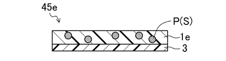
- Legal status (The legal status is an assumption and is not a legal conclusion. Google has not performed a legal analysis and makes no representation as to the accuracy of the status listed.)
- Ceased
Links
Images






Classifications
-
- G—PHYSICS
- G02—OPTICS
- G02B—OPTICAL ELEMENTS, SYSTEMS OR APPARATUS
- G02B1/00—Optical elements characterised by the material of which they are made; Optical coatings for optical elements
- G02B1/10—Optical coatings produced by application to, or surface treatment of, optical elements
- G02B1/11—Anti-reflection coatings
-
- G—PHYSICS
- G02—OPTICS
- G02B—OPTICAL ELEMENTS, SYSTEMS OR APPARATUS
- G02B5/00—Optical elements other than lenses
- G02B5/02—Diffusing elements; Afocal elements
-
- G—PHYSICS
- G09—EDUCATION; CRYPTOGRAPHY; DISPLAY; ADVERTISING; SEALS
- G09F—DISPLAYING; ADVERTISING; SIGNS; LABELS OR NAME-PLATES; SEALS
- G09F9/00—Indicating arrangements for variable information in which the information is built-up on a support by selection or combination of individual elements
- G09F9/30—Indicating arrangements for variable information in which the information is built-up on a support by selection or combination of individual elements in which the desired character or characters are formed by combining individual elements
- G09F9/302—Indicating arrangements for variable information in which the information is built-up on a support by selection or combination of individual elements in which the desired character or characters are formed by combining individual elements characterised by the form or geometrical disposition of the individual elements
- G09F9/3026—Video wall, i.e. stackable semiconductor matrix display modules
-
- Y—GENERAL TAGGING OF NEW TECHNOLOGICAL DEVELOPMENTS; GENERAL TAGGING OF CROSS-SECTIONAL TECHNOLOGIES SPANNING OVER SEVERAL SECTIONS OF THE IPC; TECHNICAL SUBJECTS COVERED BY FORMER USPC CROSS-REFERENCE ART COLLECTIONS [XRACs] AND DIGESTS
- Y10—TECHNICAL SUBJECTS COVERED BY FORMER USPC
- Y10T—TECHNICAL SUBJECTS COVERED BY FORMER US CLASSIFICATION
- Y10T428/00—Stock material or miscellaneous articles
- Y10T428/24—Structurally defined web or sheet [e.g., overall dimension, etc.]
- Y10T428/24355—Continuous and nonuniform or irregular surface on layer or component [e.g., roofing, etc.]
-
- Y—GENERAL TAGGING OF NEW TECHNOLOGICAL DEVELOPMENTS; GENERAL TAGGING OF CROSS-SECTIONAL TECHNOLOGIES SPANNING OVER SEVERAL SECTIONS OF THE IPC; TECHNICAL SUBJECTS COVERED BY FORMER USPC CROSS-REFERENCE ART COLLECTIONS [XRACs] AND DIGESTS
- Y10—TECHNICAL SUBJECTS COVERED BY FORMER USPC
- Y10T—TECHNICAL SUBJECTS COVERED BY FORMER US CLASSIFICATION
- Y10T428/00—Stock material or miscellaneous articles
- Y10T428/28—Web or sheet containing structurally defined element or component and having an adhesive outermost layer
- Y10T428/2848—Three or more layers
Definitions
- the present invention relates to a plastic film, a display device, and a multi-display device, and more particularly to a multi-display device, a display device constituting the multi-display device, and a plastic film for suppressing reflection of external light used for them.
- Patent Document 1 discloses a display device in which a magnifying lens is provided at a joint between adjacent monitors.
- a frame-shaped lens member whose cross section is formed in a substantially semicircular shape at the periphery of each display device Is often placed.
- reflection of external light on the surface of the lens member may be affixed to suppress reflection on the surface of the lens member.
- the surface of the lens member is formed in a curved surface shape, in particular, in the corner portion of the frame-shaped lens member, for example, by having a surface shape in which two different curved surfaces are connected, Wrinkles and the like are easily generated on the attached plastic film, and it is difficult to attach the plastic film.
- the present invention has been made in view of such a point, and an object of the present invention is to easily attach a plastic film for suppressing reflection of external light.
- the present invention provides heat shrinkability to a plastic film for suppressing reflection of external light.
- the plastic film according to the present invention includes a base film having heat shrinkability and a reflection suppressing portion that suppresses reflection of external light provided on the base film.
- the base film since the reflection of an external light is suppressed by the reflection suppression part provided in the base film, and the base film has heat shrinkability, in order to suppress the reflection of external light Heat shrinkability is imparted to the plastic film. Therefore, when affixing the plastic film to a curved surface to be applied, for example, an object having an application surface inside a cylindrical plastic film is coated with an ultraviolet curable or thermosetting resin coating film. When the plastic film is heated in a state of being disposed via the adhesive film or the like, the base film constituting the plastic film is thermally contracted, and the plastic film is uniformly adhered to the surface to be adhered. Thereby, since a plastic film is easily affixed on a to-be-attached surface, even if a to-be-attached surface is a curved surface shape, the plastic film for suppressing reflection of external light is easily attached.
- the reflection suppression portion may be formed of a reflection suppression film that suppresses reflection of external light provided on the surface of the base film.
- the reflection suppression part is comprised by the reflection suppression film
- the antireflection film is an antiglare film that has been subjected to unevenness provided on the surface of the base film, an antireflector film in which a plurality of dielectric films are laminated, or the antiglare film and the antireflector film are laminated in order. You may be comprised by the laminated film.
- the anti-glare film provided on the surface of the base film and subjected to the uneven treatment the anti-reflector film provided on the surface of the base film and laminated with a plurality of dielectric films, or the base film
- the antireflection film is configured by the laminated film that is provided on the surface and in which the antiglare film and the antireflector film are laminated in order, the substrate film and the antiglare film laminated thereon are laminated to the substrate film.
- the anti-reflector film, or the base film and the anti-glare film and anti-reflector film laminated thereon specifically constitute a plastic film for suppressing reflection of external light.
- the antireflection film includes a thermoplastic resin film provided on the surface of the base film, and particles dispersed in the resin film and suppressing reflection of external light by light scattering on the particle surface. Also good.
- membrane suppresses reflection of external light by providing the resin film which has the thermoplastic resin provided in the surface of the base film, and the particle
- the plastic film is made up of a base film and a resin film in which particles are dispersed by being laminated on the base film, so that even if the base film has a high thermal shrinkage rate, the resin film can be used for the thermal contraction of the base film. Will follow easily.
- the reflection suppressing portion may be composed of particles dispersed in the base film and suppressing reflection of external light by light scattering on the particle surface.
- the reflection suppression part is the particle
- the back surface of the base film may be provided with an adhesive film, and the reflection suppressing portion may be composed of particles that are dispersed in the adhesive film and suppress external light reflection by light scattering on the particle surface.
- the reflection suppression part is the particle
- the part follows easily.
- An adhesive film may be provided on the back surface of the base film.
- the adhesive film is provided in the back surface of the base film, it is between the base film which comprises the plastic film for suppressing reflection of external light, and a curved to-be-coated surface. An adhesive film is easily disposed.
- the display device is provided in a frame shape so as to cover a display panel having a display region for displaying an image and a peripheral portion of the display panel, and display light in the peripheral portion of the display region of the display panel.
- the plastic film for suppressing the reflection of the external light which covers the surface of a lens member reflection of external light is suppressed by the reflection suppression part provided in the base film, and a base film is Since it is heat-shrinkable (for example, when it is pasted and attached), for example, the lens member is placed inside a plastic film made into a cylindrical shape with an ultraviolet curable resin or a thermosetting resin. Inferring that the plastic film is heat-shrinked by heating the plastic film in a state where it is disposed through a coating film or an adhesive film, so that the plastic film is uniformly adhered to the lens member. Is done. As a result, it can be said that the plastic film can be easily attached to the surface of the lens member. Therefore, the plastic film for suppressing the reflection of external light to the lens member provided to cover the peripheral portion of the display panel. Is easily pasted.
- the lens member may include four linear portions that form four sides of a rectangle and four corner portions that connect the adjacent linear portions to each other.
- a lens member is provided with four linear parts and four corner
- the operation of attaching the plastic film to the lens member is facilitated.
- the base film which does not have heat shrinkability.
- the multi-display device may include a plurality of the display devices described above, and the plurality of display devices may be provided in a matrix.
- each display device in each display device, a plastic film for suppressing reflection of external light is easily attached to the lens member provided so as to cover the peripheral portion of the display panel.
- a seamless (large) screen is realized in which the joint between the display devices is not conspicuous.
- the plastic film for suppressing light reflection since the heat shrinkability is imparted to the plastic film for suppressing light reflection, the plastic film for suppressing light reflection can be easily attached.
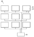
- FIG. 1 is a plan view of the multi-display device according to the first embodiment.
- FIG. 2 is a schematic configuration diagram of the multi-display device according to the first embodiment.
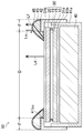
- FIG. 3 is a cross-sectional view of the liquid crystal display device constituting the multi-display device according to the first embodiment.
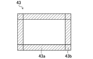
- FIG. 4 is a plan view of a lens member constituting the liquid crystal display device according to the first embodiment.
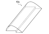
- FIG. 5 is a perspective view of a linear portion constituting the lens member according to the first embodiment.
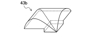
- FIG. 6 is a perspective view of a corner portion constituting the lens member according to the first embodiment.
- FIG. 7 is a cross-sectional view of a plastic film constituting the liquid crystal display device according to the first embodiment.
- FIG. 8 is a cross-sectional view of a first modification of the plastic film constituting the liquid crystal display device according to the first embodiment.
- FIG. 9 is a cross-sectional view of a second modification of the plastic film constituting the liquid crystal display device according to the first embodiment.
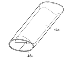
- FIG. 10 is a perspective view illustrating a method of attaching a plastic film to the linear portion of the lens member according to the first embodiment.
- FIG. 11 is a perspective view illustrating a method of attaching a plastic film to the corner of the lens member according to the first embodiment.
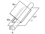
- FIG. 12 is a perspective view illustrating another method of attaching a plastic film to the linear portion of the lens member according to the first embodiment.
- FIG. 13 is a cross-sectional view of a plastic film according to the second embodiment.
- FIG. 14 is a cross-sectional view of the plastic film according to the third embodiment.
- FIG. 15 is a cross-sectional view of a plastic film according to the fourth embodiment.
- Embodiment 1 of the Invention 1 to 12 show Embodiment 1 of a plastic film, a display device and a multi-display device according to the present invention.
- FIG. 1 is a plan view of the multi-display device 60 of the present embodiment.
- FIG. 2 is a schematic configuration diagram of the multi-display device 60.
- FIG. 3 is a cross-sectional view of the liquid crystal display device 50 that constitutes the multi-display device 60.
- FIG. 4 is a plan view of the lens member 43 constituting the liquid crystal display device 50.
- FIG. 5 is a perspective view of the linear portion 43 a constituting the lens member 43.
- FIG. 6 is a perspective view of a corner portion 43 b constituting the lens member 43.
- FIG. 1 is a plan view of the multi-display device 60 of the present embodiment.
- FIG. 2 is a schematic configuration diagram of the multi-display device 60.
- FIG. 3 is a cross-sectional view of the liquid crystal display device 50 that constitute
- FIG. 7 is a cross-sectional view of a plastic film 45a for forming the plastic film 45 constituting the liquid crystal display device 50.
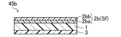
- FIG. 8 is a cross-sectional view of a plastic film 45b which is a first modification of the plastic film 45a.
- FIG. 9 is a cross-sectional view of a plastic film 45c which is a second modification of the plastic film 45a.
- the multi-display device 60 controls 3 ⁇ 3 (9) liquid crystal display devices 50 arranged in a matrix and controls each liquid crystal display device 50.
- the configuration in which the liquid crystal display devices 50 are connected in parallel is illustrated.
- the liquid crystal display devices 50 may be connected in series by a GPIB (General Purpose Interface Interface Bus) interface board or the like. .
- GPIB General Purpose Interface Interface Bus
- the control unit 55 is configured to transmit content to be displayed on each liquid crystal display device 50 and to switch display modes in each liquid crystal display device 50.
- the multi-display device 60 displays one image as a whole (with nine liquid crystal display devices 50) based on the signal from the control unit 55, or the same or different in each liquid crystal display device 50. It is configured to display different images.
- the frame is configured to be disassembled into a plurality of pieces, and can be freely changed in size according to the number of the liquid crystal display devices 50.
- the liquid crystal display device 50 includes a liquid crystal display panel 30 and a pair of polarizing plates 31a and 31b attached to the back surface (lower side in the figure) and front surface (upper side in the figure) of the liquid crystal display panel 30.
- a backlight 40 provided on the back side of the liquid crystal display panel 30, an optical sheet (not shown) such as a diffusion sheet provided between the liquid crystal display panel 30 and the backlight 40, a liquid crystal display panel 30, and a pair Polarizing plates 31 a and 31 b, the backlight 40 and the lower casing 41 a and the upper casing 41 b provided so as to accommodate the optical sheet therein, and the polarizing plate 31 a and the adhesive film 42 on the peripheral portion of the liquid crystal display panel 30.
- a plastic film 45 provided so as to cover the surface of the lens member 43. 1 and 2, the broken line in each liquid crystal display device 50 indicates the inner peripheral edge of the plastic film 45 attached to the surface of the lens member 43.
- the liquid crystal display panel 30 includes an active matrix substrate 10 and a counter substrate 20 provided so as to face each other, a liquid crystal layer 15 provided between the active matrix substrate 10 and the counter substrate 20, The active matrix substrate 10 and the counter substrate 20 are bonded to each other, and a sealing material 16 provided in a frame shape is provided between the active matrix substrate 10 and the counter substrate 20 to enclose the liquid crystal layer 15.
- the liquid crystal display panel 30 has a display area D for displaying an image inside the sealing material 16.
- the active matrix substrate 10 covers, for example, an insulating substrate (not shown) such as a glass substrate, a plurality of gate lines (not shown) provided on the insulating substrate so as to extend in parallel to each other, and the gate lines.
- a plurality of TFTs Thin-Film-Transistor, not shown
- an interlayer insulating film not shown
- a plurality of pixel electrodes (not shown) provided in a matrix on the interlayer insulating film, and an alignment film (not shown) provided so as to cover each pixel electrode.
- the counter substrate 20 includes, for example, an insulating substrate (not shown) such as a glass substrate, a black matrix (not shown) provided in a lattice shape on the insulating substrate, and a red layer provided between each lattice of the black matrix.
- a plurality of colored layers (not shown) such as a green layer and a blue layer, a common electrode (not shown) provided to cover the black matrix and each colored layer, and a plurality of columns provided on the common electrode in a column shape
- a photo spacer (not shown) and an alignment film (not shown) provided so as to cover the common electrode and each photo spacer are provided.
- the liquid crystal layer 15 is made of, for example, a nematic liquid crystal material having electro-optical characteristics.
- the backlight 40 includes, for example, a light guide plate (not shown), a light source (not shown) such as a plurality of LEDs (Light Emitting Diode) provided along one side surface of the light guide plate, and a back surface side of the light guide plate. And a reflection sheet (not shown) provided.
- a light guide plate (not shown)
- a light source such as a plurality of LEDs (Light Emitting Diode) provided along one side surface of the light guide plate, and a back surface side of the light guide plate.
- a reflection sheet not shown
- the lower housing 41a is provided so as to accommodate the backlight 40, the lower portion of the liquid crystal display panel 30 in the figure, and the polarizing plate 31a and the optical sheet between them. ing.
- the upper housing 41b is provided so as to accommodate therein the upper portion of the liquid crystal display panel 30 in the drawing, the polarizing plate 31b and the upper portion of the side wall of the lower housing 41a, and the like.
- An opening 41bc is provided on the upper surface so that the display area D of the liquid crystal display panel 40 is exposed.
- the display area D is provided in the opening 41bc of the upper housing 41b, and the frame area F is provided outside the display area D.
- the lens member 43 is provided in a frame shape, and includes four linear portions 43 a and four corners 43 b that connect the adjacent linear portions 43 a to each other. Then, as shown in FIG. 3, the lens member 43 is configured to guide the display light Lf at the periphery of the display area D of the liquid crystal display panel 30 to the outside of the display area D, that is, the frame area F by its curved surface shape. Has been.
- the linear portion 43a has a substantially semicircular cross section, and is made of, for example, a transparent resin material such as acrylic resin. Moreover, in the linear part 43a, as shown in FIG.3 and FIG.5, while the display area D side inclines relatively loosely, the frame area
- the corner portion 43 b includes two different curved surfaces of a linear portion 43 a extending in the vertical direction (see FIG. 4) and a curved surface of the linear portion 43 a extending in the horizontal direction (see FIG. 4).
- the curved surface has a connected surface shape and is made of a transparent resin material such as an acrylic resin.
- the adhesive film 42 is made of, for example, an ultraviolet curable or thermosetting transparent resin material.
- the plastic film 45a constituting the plastic film 45 includes a base film 1 having heat shrinkability, an anti-glare film 2a provided on the surface of the base film 1 as a reflection suppressing film Sf, And an adhesive film 3 provided on the back surface of the material film 1.
- the plastic film 45 in FIGS. 1 to 3 is a plastic film 45 a thermally contracted on the surface of the lens member 43.
- the reflection suppression part which suppresses reflection of the external light Lo is comprised by the reflection suppression film
- the base film 1 is a uniaxially or biaxially stretched film (for example, a thickness of about 100 ⁇ m) such as polyvinyl chloride, polyethylene, polypropylene, polyethylene terephthalate, or the like.
- the anti-glare film 2a is a film (for example, a thickness of about 10 ⁇ m) whose surface is roughened (for example, an average roughness (Ra) of about 10 ⁇ m) by, for example, sandblasting, embossing roll, etching, or the like. Further, as shown in FIG. 3, the antiglare film 2a is configured to suppress reflection of the external light Lo by its surface shape.
- the adhesive film 3 is made of, for example, an acrylic resin material.
- the plastic film 45a provided with the anti-glare film 2a is exemplified as the antireflection film Sf.
- the plastic film 45b provided with the anti-reflector film 2b as the antireflection film Sf (FIG. 8)
- a plastic film 45c (see FIG. 9) provided with a laminated film 2 of an antiglare film 2a and an antireflector film 2b may be used as the antireflection film Sf.
- the plastic film 45 b includes a base film 1 having heat shrinkability, an anti-reflector film 2 b provided as a reflection suppression film Sf on the surface of the base film 1, and a base material And an adhesive film 3 provided on the back surface of the film 1.
- the anti-reflector film 2b includes a first dielectric film 2ba having a relatively high refractive index and a second dielectric film 2bb having a relatively low refractive index.
- the anti-reflector film 2b is configured to suppress reflection of external light Lo by forming an optical interference layer by a laminated film of a plurality of derivative films having different refractive indexes.
- the first dielectric film 2ba and the second dielectric 2bb are each configured to have a thickness of about 0.1 ⁇ m by, for example, various fluoropolymers having different refractive indexes.
- the plastic film 45c is a laminate of a base film 1 having heat shrinkability and an anti-glare film 2a and an anti-reflector film 2b provided as a reflection suppressing film Sf on the surface of the base film 1.
- a film 2 and an adhesive film 3 provided on the back surface of the base film 1 are provided.
- the liquid crystal layer 15 disposed between each pixel electrode on the active matrix substrate 10 and the common electrode on the counter substrate 20 has a predetermined value for each subpixel.
- the transmittance of light from the backlight 45 is adjusted to each subpixel, and the display light Ld is emitted in the display region D as shown in FIG.
- the display light Lf is emitted from the frame region F.
- the display light Lf at the periphery of the display region D is enlarged and emitted to the outside (the frame region F side).
- FIG. 10 is a perspective view showing a method of attaching the plastic film 45 a to the linear portion 43 a of the lens member 43.
- FIG. 11 is a perspective view showing a method of attaching a plastic film 45 a to the corner 43 b of the lens member 43.
- FIG. 12 is a perspective view showing another method of attaching the plastic film 45 a to the linear portion 43 a of the lens member 43.
- the manufacturing method of the present embodiment includes a liquid crystal display panel manufacturing process, a housing assembly process, a film sticking process, and a lens member mounting process.
- a large-sized active matrix mother substrate in which the active matrix substrate 10 is arranged in a matrix is formed by forming gate lines, source lines, TFTs, pixel electrodes, and the like on a glass substrate using a known method. To do.
- a black matrix, a color filter, a common electrode, and the like on a glass substrate by using a known method, a large-sized counter mother substrate in which the counter substrate 20 is arranged in a matrix is manufactured.
- the sealing material 16 is drawn in a frame shape on the surface of each counter substrate 20 of the counter mother substrate using, for example, a dispenser.
- the large-sized bonded body is divided into cell units to produce a liquid crystal display panel 30, and polarizing plates 31a and 31b are attached to the back and front surfaces of the liquid crystal display panel 30, and further, TCP (Tape Carrier Carrier Package) ) And PWB (Printed Wiring Board).
- TCP Transmission Carrier Carrier Package
- PWB Print Wiring Board
- the liquid crystal display panel 30 on which the polarizing plates 31a and 31b are attached and TCP or PWB is mounted can be manufactured.
- ⁇ Case assembly process> A lower casing 41a, an upper casing 41b, a backlight 40, and an optical sheet are prepared, and the backlight 40, the optical sheet, and the polarizing plate manufactured in the liquid crystal display panel manufacturing process are provided inside the lower casing 41a. After the liquid crystal display panel 30 with 31a and 31b attached is assembled and the backlight 40 and the liquid crystal display panel 30 are fixed, the upper casing 41b is fitted into the upper part of the side wall of the lower casing 41a.
- the plastic film 45a is heated and the plastic film 45a is thermally contracted.
- the chamber is evacuated.
- the plastic film 45a is heated and the plastic film 45a is thermally contracted.
- plastic film 45a on the side surface that is upright with respect to the bottom surface and the bottom surface of the corner portion 43b (contacts the linear portion 43a) is removed.
- the method of attaching the heat-shrinkable plastic film 45a to the linear portion 43a has been exemplified.
- a non-heat-shrinkable plastic film (45n) is attached to the linear portion 43a.
- the peripheral wall of the roll R that can be raised and lowered while placing the linear portion 43a on the slidable table T and applying the plastic film 45n to the surface of the linear portion 43a.
- the plastic film 45n is affixed on the peripheral surface of the linear part 43a.
- the plastic film 45n is obtained, for example, by omitting the base film 1 having heat shrinkability in the plastic film 45a, and corresponds to a general antireflection (suppression) film. Further, as shown in FIG. 12, a step is formed on the surface of the table T so as to fit into the shape of the bottom surface of the linear portion 43a. Further, the table T is configured to vacuum-suck the linear portion 43a on the surface thereof.
- the manufacturing method in which the plastic film 45a is attached to the surface of the lens member 43 via the adhesive film 3 provided on the back surface of the plastic film 45a is exemplified.
- the adhesive film 3 on the back surface of the plastic film 45a is illustrated. Is applied to the surface of the lens member 43, for example, by applying an ultraviolet curable or thermosetting transparent resin material, and the plastic film 45a is thermally contracted, and then the temperature is higher than the temperature at the time of thermal contraction. Heating or ultraviolet irradiation may be performed.
- the lens member 43 (the linear portion 43a and the corner portion 43b) to which the plastic film 45a is attached can be manufactured.
- the upper surface of the upper casing 41b of the casing in which the backlight 40, the liquid crystal display panel 30, and the like are incorporated in the casing assembling step, and the peripheral edge of the polarizing plate 31b exposed from the opening 41bc are, for example, ultraviolet curable or After applying a thermosetting transparent resin material and placing the lens member 43 on which the plastic film 45a is attached in the film application step on the application surface, the adhesive film 42 is irradiated with ultraviolet rays or heated. And the lens member 43 is attached to the upper housing 41b and the polarizing plate 31b.
- the adhesive film 42 is exemplified by an ultraviolet curable or thermosetting transparent resin material, but may be a two-component room temperature curable resin material that is cured by natural drying.
- the liquid crystal display device 50 of the present embodiment can be manufactured.
- the plastic film 45a for suppressing the reflection of the external light Lo covering the surface of the lens member 43 is provided on the base film 1.
- the reflection suppression film Sf thus formed suppresses the reflection of the external light Lo, and the base film 1 has the heat shrinkability. Therefore, the plastic film 45a for suppressing the reflection of the external light Lo has the heat shrinkability. Has been granted. Therefore, when the plastic film 45a is attached to the surface of the lens member 43, the plastic film 45a is placed in a state where the linear portions 43a and the corner portions 43b of the lens member 43 are disposed inside the cylindrical plastic film 45a.
- the base film 1 which comprises the plastic film 45a is heat-shrinked, and the plastic film 45a adheres
- the plastic film 45a can be easily attached to the application surfaces of the linear portions 43a and the corner portions 43b constituting the lens member 43, the application surface of the lens member 43 is curved.
- the plastic film 45a for suppressing the reflection of the external light Lo can be easily attached.
- the plastic film 45a of this embodiment since the adhesive film 3 is provided on the back surface of the base film 1, the base film 1 constituting the plastic film 45 for suppressing the reflection of the external light Lo. It is possible to easily dispose the adhesive film 3 between the curved lens member 43 and the surface to be bonded.
- the lens member 43 since the lens member 43 includes the four linear portions 43a and the four corner portions 43b, each linear portion 43a and each corner constituting the lens member 43. Affixing the plastic film 45a to the lens member 43 can be facilitated by affixing the plastic film 45a for suppressing reflection of the external light Lo for each portion 43b.
- the reflection of the external light Lo is suppressed with respect to the lens member 43 provided so as to cover the peripheral portion of the liquid crystal display panel 30. Since the plastic film 45a can be easily attached, it is possible to easily realize a large screen where the joints between the liquid crystal display devices 50 are inconspicuous (seamless).
- the liquid crystal display device 50 in which the outer peripheral edge of the upper housing 41b and the outer peripheral edge of the lens member 43 including the plastic film 45a coincide with each other is illustrated. It may be a liquid crystal display device arranged on the inner side of the peripheral edge, or a liquid crystal display device in which the outer peripheral edge of the lens member is arranged outside the outer peripheral edge of the housing.
- FIG. 13 is a cross-sectional view of the plastic film 45d of this embodiment.
- the same portions as those in FIGS. 1 to 12 are denoted by the same reference numerals, and detailed description thereof is omitted.
- the base film 1 is provided with the anti-glare film 2a, the anti-reflector film 2b, and the laminated film 2 of the anti-glare film 2a and the anti-reflector film 2b as the anti-reflection film (reflection suppressing part) Sf.
- the films 45a to 45c are respectively illustrated, in the present embodiment, a plastic film 45d in which the resin film 2c in which the antiglare particles P are dispersed is provided as the reflection suppressing film (reflection suppressing portion) Sf on the base film 1 is illustrated. To do.
- the plastic film 45 d includes a base film 1 having heat shrinkability, a resin film 2 c provided as a reflection suppression film Sf on the surface of the base film 1, and a back surface of the base film 1. And an adhesive film 3 provided.
- the resin film 2c is made of, for example, polyvinyl chloride, polyethylene, polypropylene, or the like, and has thermoplasticity. Antiglare particles P are dispersed in the resin film 2c.
- the anti-glare particles P are composed of, for example, silica particles having a particle diameter of about 3 ⁇ m, and are configured to suppress reflection of the external light Lo by light scattering on the surface thereof.
- the plastic film 45d of this embodiment since the heat shrinkability is imparted to the plastic film 45d as in the first embodiment, the surface to be adhered of the lens member 43 is curved. Even if it exists, the plastic film 45d for suppressing reflection of external light Lo can be easily affixed.
- the antireflection film Sf includes the thermoplastic resin film 2c provided on the surface of the base film 1 and the antiglare particles P dispersed in the resin film 2c. Therefore, the plastic film 45d for suppressing the reflection of the external light Lo is composed of the base film 1 and the resin film 2c laminated thereon and the anti-glare particles P dispersed therein. Even if the thermal contraction rate of the resin film 2 is high, the resin film 2 c (reflection suppression film Sf) can easily follow the thermal contraction of the base film 1.
- FIG. 14 is a cross-sectional view of the plastic film 45e of this embodiment.
- the plastic film 45d in which the antiglare particles P are dispersed in the resin film 2c is illustrated.
- the plastic film 45e in which the antiglare particles P are dispersed in the base film 1e is illustrated.
- the plastic film 45e includes a base film 1e having heat shrinkability, an antiglare particle P provided as an antireflection portion S inside the base film 1e, and a back surface of the base film 1e. And an adhesive film 3 provided.
- the base film 1e is a uniaxially or biaxially stretched film (for example, about 100 ⁇ m thick) such as polyvinyl chloride, polyethylene, polypropylene, polyethylene terephthalate, or the like.
- the heat shrinkability is imparted to the plastic film 45e as in the first and second embodiments. Even if it is a shape, the plastic film 45e for suppressing reflection of the external light Lo can be easily attached.
- the antireflection part S is the anti-glare particles P dispersed in the base film 1e, the base film 1e even if the base film 1e has a high thermal shrinkage rate.
- the reflection suppressing portion S can easily follow the heat shrinkage.
- FIG. 15 is a cross-sectional view of the plastic film 45f of the present embodiment.
- the plastic film 45e in which the antiglare particles P are dispersed in the base film 1e is illustrated.
- the plastic film 45f in which the antiglare particles P are dispersed in the adhesive film 3f is illustrated.
- the plastic film 45 f is provided as a heat-shrinkable base film 1, an adhesive film 3 f provided on the back surface of the base film 1, and an antireflection part S in the adhesive film 3 f.
- Anti-glare particles P are provided as a heat-shrinkable base film 1, an adhesive film 3 f provided on the back surface of the base film 1, and an antireflection part S in the adhesive film 3 f.
- Anti-glare particles P is provided as a heat-shrinkable base film 1, an adhesive film 3 f provided on the back surface of the base film 1, and an antireflection part S in the adhesive film 3 f.
- Anti-glare particles P are examples of the plastic film 45 f.
- the adhesive film 3f is made of, for example, an acrylic resin material.
- the heat shrinkability is imparted to the plastic film 45f as in the first to third embodiments. Even if it is a shape, the plastic film 45f for suppressing reflection of the external light Lo can be easily attached.
- the reflection suppression part S is the anti-glare particle P disperse
- the thermal contraction rate of the base film 1 is high.
- the reflection suppression part S can be made to follow the thermal contraction of the base film 1 easily.
- the plastic films 45d to 45f in which the antiglare particles P are substantially uniformly dispersed are exemplified.
- the heat treatment is performed so that the particle density of the antiglare particles is uniform when the antiglare particles are thermally contracted on the surface to be bonded.
- the particle density of the antiglare particles in the plastic film before shrinking may be distributed according to the surface shape of the adherend surface.
- a liquid crystal display device has been exemplified as the display device.
- the present invention can be applied to an organic EL (Electro Luminescence) display device, an inorganic EL display device, an electrophoretic display device, a plasma display (PD). )) Devices, plasma addressed liquid crystal display (PALC) devices, field emission display (FED) devices, surface electric field display (SED) devices, etc. It can also be applied to other display devices.
- organic EL Electro Luminescence
- PLC plasma addressed liquid crystal display
- FED field emission display
- SED surface electric field display
- the display device using the color filter method is exemplified, but the present invention can also be applied to a display device using the field sequential method.
- the present invention can easily affix a plastic film for suppressing reflection of external light even if the surface to be adhered is a curved surface. It is useful not only as a reflection suppression means for a display device provided, but also as a reflection suppression means for a picture frame or a vase.
Landscapes
- Physics & Mathematics (AREA)
- General Physics & Mathematics (AREA)
- Optics & Photonics (AREA)
- Liquid Crystal (AREA)
- Devices For Indicating Variable Information By Combining Individual Elements (AREA)
Abstract
熱収縮性を有する基材フィルム(1)と、基材フィルム(1)に設けられた外光の反射を抑制する反射抑制部(Sf)とを備えている。
Description
本発明は、プラスチックフィルム、表示装置及びマルチディスプレイ装置に関し、特に、マルチディスプレイ装置及びそれを構成する表示装置、並びにそれらに用いる外光の反射を抑制するためのプラスチックフィルムに関するものである。
近年、デジタルサイネージ(電子看板)などの用途の大規模な表示装置として、複数の表示装置をマトリクス状に配置させたマルチディスプレイ装置が注目されている。
例えば、特許文献1には、隣接するモニタ間の目地部分に拡大レンズが設けられたディスプレイ装置が開示されている。
ところで、マルチディスプレイ装置では、特許文献1のように、各表示装置の継ぎ目が視認され難くするために、各表示装置の周縁部に横断面が略半円状に形成された枠状のレンズ部材を配置させることが多い。そして、そのマルチディスプレイ装置を構成する各表示装置では、レンズ部材の表面に外光の反射を抑制するためのプラスチックフィルムを貼り付けることにより、レンズ部材の表面への写り込みを抑制することがある。ここで、レンズ部材の表面は、曲面状に形成されているので、特に、例えば、枠状のレンズ部材の角部では、互いに異なる2つの曲面が連結した表面形状を有していることにより、貼り付けたプラスチックフィルムにシワなどが発生し易く、プラスチックフィルムの貼り付けが困難である。
本発明は、かかる点に鑑みてなされたものであり、その目的とするところは、外光の反射を抑制するためのプラスチックフィルムを容易に貼り付けることにある。
上記目的を達成するために、本発明は、外光の反射を抑制するためのプラスチックフィルムに熱収縮性を付与するようにしたものである。
具体的に本発明に係るプラスチックフィルムは、熱収縮性を有する基材フィルムと、上記基材フィルムに設けられた外光の反射を抑制する反射抑制部とを備えている。
上記の構成によれば、基材フィルムに設けられた反射抑制部により、外光の反射が抑制され、基材フィルムが熱収縮性を有しているので、外光の反射を抑制するためのプラスチックフィルムに熱収縮性が付与されている。そのため、そのプラスチックフィルムを曲面状の被貼付面に貼り付ける場合には、例えば、筒状にしたプラスチックフィルムの内部に被貼付面を有する対象物を紫外線硬化型又は熱硬化型の樹脂の塗布膜や粘着膜などを介して配置した状態でプラスチックフィルムを加熱することにより、プラスチックフィルムを構成する基材フィルムが熱収縮して、プラスチックフィルムが被貼付面に均一に密着することになる。これにより、プラスチックフィルムが被貼付面に容易に貼り付けられるので、被貼付面が曲面状であっても、外光の反射を抑制するためのプラスチックフィルムが容易に貼り付けられる。
上記反射抑制部は、上記基材フィルムの表面に設けられた外光の反射を抑制する反射抑制膜により構成されていてもよい。
上記の構成によれば、反射抑制部が基材フィルムの表面に設けられた外光の反射を抑制する反射抑制膜により構成されているので、基材フィルムとそれに積層された反射抑制膜とにより、外光の反射を抑制するためのプラスチックフィルムが具体的に構成される。
上記反射抑制膜は、上記基材フィルムの表面に設けられた凹凸処理されたアンチグレア膜、複数の誘電体膜が積層されたアンチリフレクタ膜、又は該アンチグレア膜及び該アンチリフレクタ膜が順に積層された積層膜により構成されていてもよい。
上記の構成によれば、基材フィルムの表面に設けられ、凹凸処理されたアンチグレア膜、基材フィルムの表面に設けられ、複数の誘電体膜が積層されたアンチリフレクタ膜、又は基材フィルムの表面に設けられ、アンチグレア膜及びアンチリフレクタ膜が順に積層された積層膜により、反射抑制膜が構成されているので、基材フィルムとそれに積層されたアンチグレア膜とにより、基材フィルムとそれに積層されたアンチリフレクタ膜とにより、又は基材フィルムとそれに積層されたアンチグレア膜及びアンチリフレクタ膜とにより、外光の反射を抑制するためのプラスチックフィルムが具体的に構成される。
上記反射抑制膜は、上記基材フィルムの表面に設けられた熱可塑性を有する樹脂膜と、該樹脂膜に分散され、粒子表面における光散乱により外光の反射を抑制する粒子とを備えていてもよい。
上記の構成によれば、反射抑制膜が、基材フィルムの表面に設けられた熱可塑性を有する樹脂膜とその樹脂膜に分散された粒子とを備えていることにより、外光の反射を抑制するためのプラスチックフィルムが基材フィルムとそれに積層されて粒子が分散された樹脂膜とにより構成されているので、基材フィルムの熱収縮率が高くても、基材フィルムの熱収縮に樹脂膜が容易に追従することになる。
上記反射抑制部は、上記基材フィルムに分散され粒子表面における光散乱により外光の反射を抑制する粒子により構成されていてもよい。
上記の構成によれば、反射抑制部が基材フィルムに分散された粒子であるので、基材フィルムの熱収縮率が高くても、基材フィルムの熱収縮に反射抑制部が容易に追従することになる。
上記基材フィルムの裏面には、粘着膜が設けられ、上記反射抑制部は、上記粘着膜に分散され粒子表面における光散乱により外光の反射を抑制する粒子により構成されていてもよい。
上記の構成によれば、反射抑制部が基材フィルムに積層された粘着膜に分散された粒子であるので、基材フィルムの熱収縮率が高くても、基材フィルムの熱収縮に反射抑制部が容易に追従することになる。
上記基材フィルムの裏面には、粘着膜が設けられていてもよい。
上記の構成によれば、基材フィルムの裏面に粘着膜が設けられているので、外光の反射を抑制するためのプラスチックフィルムを構成する基材フィルムと曲面状の被貼付面との間に容易に粘着膜が配置される。
また、本発明に係る表示装置は、画像表示を行う表示領域を有する表示パネルと、上記表示パネルの周縁部を覆うように枠状に設けられ、上記表示パネルの表示領域の周縁部における表示光を該表示領域の外側に導くレンズ部材と、上記レンズ部材の表面を覆うように設けられ、熱収縮した基材フィルム、及び該基材フィルムに設けられた外光の反射を抑制する反射抑制部を含むプラスチックフィルムとを備えている。
上記の構成によれば、レンズ部材の表面を覆う外光の反射を抑制するためのプラスチックフィルムでは、基材フィルムに設けられた反射抑制部により、外光の反射が抑制され、基材フィルムが(例えば、貼り付ける前に熱収縮性を有し、貼り付ける際に)熱収縮しているので、例えば、筒状にしたプラスチックフィルムの内部にレンズ部材を紫外線硬化型又は熱硬化型の樹脂の塗布膜や粘着膜などを介して配置した状態でプラスチックフィルムを加熱することにより、プラスチックフィルムを構成する基材フィルムが熱収縮して、プラスチックフィルムがレンズ部材に均一に密着している、と推察される。これにより、プラスチックフィルムがレンズ部材の表面に容易に貼り付けられる、と言えるので、表示パネルの周縁部を覆うように設けられたレンズ部材に対して、外光の反射を抑制するためのプラスチックフィルムが容易に貼り付けられる。
上記レンズ部材は、矩形の4辺を構成する4つの線状部と、隣り合う該各線状部を互いにそれぞれ連結する4つの角部とを備えていてもよい。
上記の構成によれば、レンズ部材が4つの線状部と4つの角部とを備えているので、レンズ部材を構成する各線状部及び各角部毎に外光の反射を抑制するためのプラスチックフィルムを貼り付けることにより、レンズ部材に対するプラスチックフィルムの貼付作業が容易になる。なお、レンズ部材を構成する各線状部については、曲面の形状が単純なので、熱収縮性を有しない基材フィルムを用いてもよい。
また、本発明に係るマルチディスプレイ装置は、上述した表示装置を複数有し、上記複数の表示装置は、マトリクス状に設けられていてもよい。
上記の構成によれば、各表示装置において、表示パネルの周縁部を覆うように設けられたレンズ部材に対して、外光の反射を抑制するためのプラスチックフィルムが容易に貼り付けられるので、各表示装置の間の継ぎ目が目立たない(シームレスの)大画面化が実現する。
本発明によれば、光反射を抑制するためのプラスチックフィルムに熱収縮性が付与されているので、光反射を抑制するためのプラスチックフィルムを容易に貼り付けることができる。
以下、本発明の実施形態を図面に基づいて詳細に説明する。なお、本発明は、以下の各実施形態に限定されるものではない。
《発明の実施形態1》
図1~図12は、本発明に係るプラスチックフィルム、表示装置及びマルチディスプレイ装置の実施形態1を示している。具体的に、図1は、本実施形態のマルチディスプレイ装置60の平面図である。また、図2は、マルチディスプレイ装置60の構成概略図である。また、図3は、マルチディスプレイ装置60を構成する液晶表示装置50の断面図である。また、図4は、液晶表示装置50を構成するレンズ部材43の平面図である。また、図5は、レンズ部材43を構成する線状部43aの斜視図である。また、図6は、レンズ部材43を構成する角部43bの斜視図である。また、図7は、液晶表示装置50を構成するプラスチックフィルム45を形成するためのプラスチックフィルム45aの断面図である。また、図8は、プラスチックフィルム45aの第1の変形例であるプラスチックフィルム45bの断面図である。また、図9は、プラスチックフィルム45aの第2の変形例であるプラスチックフィルム45cの断面図である。
図1~図12は、本発明に係るプラスチックフィルム、表示装置及びマルチディスプレイ装置の実施形態1を示している。具体的に、図1は、本実施形態のマルチディスプレイ装置60の平面図である。また、図2は、マルチディスプレイ装置60の構成概略図である。また、図3は、マルチディスプレイ装置60を構成する液晶表示装置50の断面図である。また、図4は、液晶表示装置50を構成するレンズ部材43の平面図である。また、図5は、レンズ部材43を構成する線状部43aの斜視図である。また、図6は、レンズ部材43を構成する角部43bの斜視図である。また、図7は、液晶表示装置50を構成するプラスチックフィルム45を形成するためのプラスチックフィルム45aの断面図である。また、図8は、プラスチックフィルム45aの第1の変形例であるプラスチックフィルム45bの断面図である。また、図9は、プラスチックフィルム45aの第2の変形例であるプラスチックフィルム45cの断面図である。
マルチディスプレイ装置60は、図1及び図2に示すように、マトリクス状に配列するように設けられた3×3個(9個)の液晶表示装置50と、各液晶表示装置50を制御するためのコントロール部55と、各液晶表示装置50及びコントロール部55を接続する接続ケーブル51と、各液晶表示装置50を収容及び固定するように設けられた金属製のフレーム(不図示)とを備えている。なお、本実施形態では、各液晶表示装置50が並列に接続された構成を例示したが、各液晶表示装置50は、GPIB(General Purpose Interface Bus)インターフェースボードなどにより直列に接続されていてもよい。
コントロール部55は、各液晶表示装置50に表示するコンテンツを送信したり、各液晶表示装置50における表示モードの切り替えを行ったりするように構成されている。そして、これにより、マルチディスプレイ装置60は、コントロール部55からの信号に基づいて、全体で(9個の液晶表示装置50で)1つの画像を表示したり、各液晶表示装置50で同一の又は異なる画像を表示したりするように構成されている。
上記フレームは、複数個に分解できるように構成され、液晶表示装置50の構成数に応じてサイズ変更が自在に構成されている。
液晶表示装置50は、図3に示すように、液晶表示パネル30と、液晶表示パネル30の裏面(図中下側)及び表面(図中上側)に貼り付けられた一対の偏光板31a及び31bと、液晶表示パネル30の裏面側に設けられたバックライト40と、液晶表示パネル30及びバックライト40の間に設けられた拡散シートなどの光学シート(不図示)と、液晶表示パネル30、一対の偏光板31a及び31b、バックライト40並びに光学シートを内部に収容するように設けられた下側筐体41a及び上側筐体41bと、液晶表示パネル30の周縁部に偏光板31a及び接着膜42を介して枠状に設けられたレンズ部材43と、レンズ部材43の表面を覆うように設けられたプラスチックフィルム45とを備えている。なお、図1及び図2において、各液晶表示装置50内の破線は、レンズ部材43の表面に貼り付けられたプラスチックフィルム45の内周縁を示している。
液晶表示パネル30は、図3に示すように、互いに対向するように設けられたアクティブマトリクス基板10及び対向基板20と、アクティブマトリクス基板10及び対向基板20の間に設けられた液晶層15と、アクティブマトリクス基板10及び対向基板20を互いに接着すると共に、アクティブマトリクス基板10及び対向基板20の間に液晶層15を封入するために枠状に設けられたシール材16とを備えている。ここで、液晶表示パネル30は、図3に示すように、シール材16の内側に画像表示を行う表示領域Dを有している。
アクティブマトリクス基板10は、例えば、ガラス基板などの絶縁基板(不図示)と、絶縁基板上に互いに平行に延びるように設けられた複数のゲート線(不図示)と、各ゲート線を覆うように設けられたゲート絶縁膜(不図示)と、ゲート絶縁膜上に各ゲート線と直交する方向に互いに平行に延びるように設けられた複数のソース線(不図示)と、各ゲート線及び各ソース線の交差部分毎、すなわち、画像の最小単位である各副画素毎にそれぞれ設けられた複数のTFT(Thin Film Transistor、不図示)と、各TFTを覆うように設けられた層間絶縁膜(不図示)と、層間絶縁膜上にマトリクス状に設けられた複数の画素電極(不図示)と、各画素電極を覆うように設けられた配向膜(不図示)とを備えている。
対向基板20は、例えば、ガラス基板などの絶縁基板(不図示)と、絶縁基板上に格子状に設けられたブラックマトリクス(不図示)と、ブラックマトリクスの各格子間にそれぞれ設けられた赤色層、緑色層及び青色層などの複数の着色層(不図示)と、ブラックマトリクス及び各着色層を覆うように設けられた共通電極(不図示)と、共通電極上に柱状に設けられた複数のフォトスペーサ(不図示)と、共通電極及び各フォトスペーサを覆うように設けられた配向膜(不図示)とを備えている。
液晶層15は、例えば、電気光学特性を有するネマチックの液晶材料などにより構成されている。
バックライト40は、例えば、導光板(不図示)と、導光板の1つの側面に沿って設けられた複数のLED(Light Emitting Diode)などの光源(不図示)と、導光板の裏面側に設けられた反射シート(不図示)とを備えている。
下側筐体41aは、図3に示すように、バックライト40、液晶表示パネル30の図中下側部分、並びにそれらの間の偏光板31a及び光学シートなどを内部に収容するように設けられている。
上側筐体41bは、図3に示すように、液晶表示パネル30の図中上側部分、偏光板31b及び下側筐体41aの側壁の図中上側部分などを内部に収容するように設けられ、その上面に液晶表示パネル40の表示領域Dが露出するように開口部41bcが設けられている。ここで、液晶表示装置50では、図3に示すように、上側筐体41bの開口部41bcに表示領域Dが設けられ、表示領域Dの外側に額縁領域Fが設けられている。
レンズ部材43は、図4に示すように、枠状に設けられ、4つの線状部43aと、隣り合う各線状部43aを互いにそれぞれ連結する4つの角部43bとを備えている。そして、レンズ部材43は、図3に示すように、液晶表示パネル30の表示領域Dの周縁部における表示光Lfをその曲面形状により表示領域Dの外側、すなわち、額縁領域Fに導くように構成されている。
線状部43aは、図5に示すように、略半円状の横断面を有し、例えば、アクリル樹脂などの透明な樹脂材料により構成されている。また、線状部43aでは、図3及び図5に示すように、表示領域D側が相対的に緩く傾斜していると共に、額縁領域F側が相対的に急に傾斜している。
角部43bは、図6に示すように、縦方向(図4参照)に延びる線状部43aの曲面と、横方向(図4参照)に延びる線状部43aの曲面との互いに異なる2つの曲面が連結した表面形状を有し、例えば、アクリル樹脂などの透明な樹脂材料により構成されている。
接着膜42は、例えば、紫外線硬化型又は熱硬化型の透明な樹脂材料により構成されている。
プラスチックフィルム45を構成するプラスチックフィルム45aは、図7に示すように、熱収縮性を有する基材フィルム1と、基材フィルム1の表面に反射抑制膜Sfとして設けられたアンチグレア膜2aと、基材フィルム1の裏面に設けられた粘着膜3とを備えている。なお、図1~図3におけるプラスチックフィルム45は、レンズ部材43の表面で熱収縮したプラスチックフィルム45aである。また、本実施形態では、外光Loの反射を抑制する反射抑制部が反射抑制膜Sfにより構成されている。
基材フィルム1は、例えば、ポリ塩化ビニル、ポリエチレン、ポリプロピレン、ポリエチレンテレフタレートなどの1軸延伸又は2軸延伸されたフィルム(例えば、厚さ100μm程度)である。
アンチグレア膜2aは、例えば、サンドブラスト、エンボスロール、エッチングなどにより、表面が凹凸処理(例えば、平均粗さ(Ra)10μm程度)されたフィルム(例えば、厚さ10μm程度)である。また、アンチグレア膜2aは、図3に示すように、その表面形状により、外光Loの反射を抑制するように構成されている。
粘着膜3は、例えば、アクリル系の樹脂材料により構成されている。
なお、本実施形態では、反射抑制膜Sfとしてアンチグレア膜2aを備えたプラスチックフィルム45aを例示したが、プラスチックフィルム45aの代わりに、反射抑制膜Sfとしてアンチリフレクタ膜2bを備えたプラスチックフィルム45b(図8参照)、又は反射抑制膜Sfとしてアンチグレア膜2aとアンチリフレクタ膜2bとの積層膜2を備えたプラスチックフィルム45c(図9参照)を用いてもよい。
具体的に、プラスチックフィルム45bは、図8に示すように、熱収縮性を有する基材フィルム1と、基材フィルム1の表面に反射抑制膜Sfとして設けられたアンチリフレクタ膜2bと、基材フィルム1の裏面に設けられた粘着膜3とを備えている。
アンチリフレクタ膜2bは、図8に示すように、屈折率が相対的に高い第1誘電体膜2baと、屈折率が相対的に低い第2誘電体2bbとを備えている。また、アンチリフレクタ膜2bは、互いに屈折率が異なる複数の誘導体膜の積層膜により、光学干渉層が形成され、外光Loの反射を抑制するように構成されている。ここで、第1誘電体膜2ba及び第2誘電体2bbは、例えば、互いに屈折率が異なる種々のフッ素ポリマーなどにより、厚さ0.1μm程度にそれぞれ構成されている。
また、プラスチックフィルム45cは、図9に示すように、熱収縮性を有する基材フィルム1と、基材フィルム1の表面に反射抑制膜Sfとして設けられたアンチグレア膜2a及びアンチリフレクタ膜2bの積層膜2と、基材フィルム1の裏面に設けられた粘着膜3とを備えている。
上記構成の液晶表示装置50は、画像表示を行う際に、アクティブマトリクス基板10上の各画素電極と対向基板20上の共通電極との間に配置する液晶層15に各副画素毎に所定の電圧を印加して液晶層15の配向状態を変えることにより、バックライト45からの光の透過率を各副画素に調整して、図3に示すように、表示領域Dで表示光Ldを出射すると共に、額縁領域Fで表示光Lfを出射するように構成されている。なお、液晶表示装置50の額縁領域Fでは、表示領域Dの周縁部の表示光Lfが外側(額縁領域F側)に拡大して出射されている。
次に、本実施形態の液晶表示装置50の製造方法について、図10~図12を用いて説明する。ここで、図10は、レンズ部材43の線状部43aにプラスチックフィルム45aを貼り付ける方法を示す斜視図である。また、図11は、レンズ部材43の角部43bにプラスチックフィルム45aを貼り付ける方法を示す斜視図である。また、図12は、レンズ部材43の線状部43aにプラスチックフィルム45aを貼り付ける他の方法を示す斜視図である。なお、本実施形態の製造方法は、液晶表示パネル作製工程、筐体組込工程、フィルム貼付工程及びレンズ部材取付工程を備える。
<液晶表示パネル作製工程>
まず、ガラス基板上に、周知の方法を用いて、ゲート線、ソース線、TFT及び画素電極などを形成することにより、アクティブマトリクス基板10がマトリクス状に配置された大判のアクティブマトリクス母基板を作製する。
まず、ガラス基板上に、周知の方法を用いて、ゲート線、ソース線、TFT及び画素電極などを形成することにより、アクティブマトリクス基板10がマトリクス状に配置された大判のアクティブマトリクス母基板を作製する。
また、ガラス基板上に、周知の方法を用いて、ブラックマトリクス、カラーフィルタ及び共通電極などを形成することにより、対向基板20がマトリクス状に配置された大判の対向母基板を作製する。
続いて、例えば、ディスペンサを用いて、対向母基板の各対向基板20の表面にシール材16を枠状に描画する。
その後、シール材16が描画された対向母基板の各対向基板20に対し、各シール材16に囲まれた領域に液晶材料(15)を滴下する。
そして、液晶材料(15)が滴下された対向母基板とアクティブマトリクス母基板とを、減圧下で貼り合わせた後に、大気圧に開放することにより、アクティブマトリクス母基板及び対向母基板の各表面を加圧し、さらに、各シール材16を硬化させることにより、大判の貼合体を作製する。
その後、大判の貼合体を各セル単位毎に分断することにより、液晶表示パネル30を作製し、液晶表示パネル30の裏面及び表面に偏光板31a及び31bを貼り付け、さらに、TCP(Tape Carrier Package)やPWB(Printed Wiring Board)などを実装する。
以上のようにして、偏光板31a及び31bが貼り付けられ、TCPやPWBなどが実装された液晶表示パネル30を作製することができる。
<筐体組込工程>
下側筐体41a、上側筐体41b、バックライト40及び光学シートを準備し、下側筐体41aの内部に、バックライト40、光学シート、及び上記液晶表示パネル作製工程で作製された偏光板31a及び31bが貼り付けられた液晶表示パネル30を組み込み、バックライト40及び液晶表示パネル30を固定した後に、下側筐体41aの側壁の上部に上側筐体41bを嵌め込む。
下側筐体41a、上側筐体41b、バックライト40及び光学シートを準備し、下側筐体41aの内部に、バックライト40、光学シート、及び上記液晶表示パネル作製工程で作製された偏光板31a及び31bが貼り付けられた液晶表示パネル30を組み込み、バックライト40及び液晶表示パネル30を固定した後に、下側筐体41aの側壁の上部に上側筐体41bを嵌め込む。
<フィルム貼付工程>
まず、加熱装置のチャンバー内に、図10に示すように、筒状にしたプラスチックフィルム45aの内部に線状部43aを配置させた後に、チャンバー内を真空雰囲気にする。
まず、加熱装置のチャンバー内に、図10に示すように、筒状にしたプラスチックフィルム45aの内部に線状部43aを配置させた後に、チャンバー内を真空雰囲気にする。
続いて、チャンバーの内部の温度を(例えば、100℃程度)にすることにより、プラスチックフィルム45aを加熱して、プラスチックフィルム45aを熱収縮させる。
さらに、線状部43aの底面のプラスチックフィルム45aを除去する。
また、加熱装置のチャンバー内に、図11に示すように、筒状にしたプラスチックフィルム45aの内部に角部43bを配置させた後に、チャンバー内を真空雰囲気にする。
続いて、チャンバーの内部の温度を(例えば、100℃程度)にすることにより、プラスチックフィルム45aを加熱して、プラスチックフィルム45aを熱収縮させる。
さらに、角部43bの底面及び底面に対して直立した(線状部43aに当接する)側面のプラスチックフィルム45aを除去する。
なお、本実施形態では、線状部43aに熱収縮性を有するプラスチックフィルム45aを貼り付ける方法を例示したが、線状部43aに熱収縮性を有しないプラスチックフィルム(45n)を貼り付けてもよい。具体的には、図12に示すように、摺動可能なテーブルT上に線状部43aを載置し、線状部43aの表面にプラスチックフィルム45nを当てながら、昇降可能なロールRの周壁で押さえ付けることにより、線状部43aの周面にプラスチックフィルム45nを貼り付ける。ここで、プラスチックフィルム45nは、例えば、プラスチックフィルム45aにおいて、熱収縮性を有する基材フィルム1を省略したものであり、一般的な反射防止(抑制)フィルムに相当する。また、テーブルTの表面には、図12に示すように、線状部43aの底面の形状に嵌合するように、段差が形成されている。さらに、テーブルTは、その表面に線状部43aを真空吸着するように構成されている。
また、本実施形態では、プラスチックフィルム45aの裏面に設けられた粘着膜3を介してレンズ部材43の表面にプラスチックフィルム45aを貼り付ける製造方法を例示したが、プラスチックフィルム45aの裏面の粘着膜3を省略して、そのレンズ部材43の表面に、例えば、紫外線硬化型又は熱硬化型の透明な樹脂材料を塗布して、プラスチックフィルム45aを熱収縮させた後に、熱収縮時の温度よりも高温での加熱又は紫外線の照射を行ってもよい。
以上のようにして、プラスチックフィルム45aが貼り付けられたレンズ部材43(線状部43a及び角部43b)を作製することができる。
<レンズ部材取付工程>
上記筐体組込工程でバックライト40及び液晶表示パネル30などが組み込まれた筐体の上側筐体41bの上面及び開口部41bcから露出する偏光板31bの周縁部に、例えば、紫外線硬化型又は熱硬化型の透明な樹脂材料を塗布し、その塗布面に上記フィルム貼付工程でプラスチックフィルム45aが貼り付けられたレンズ部材43を配置した後に、紫外線の照射又は加熱を行うことにより、接着膜42を形成して、上側筐体41b及び偏光板31bにレンズ部材43を取り付ける。なお、本実施形態では、接着膜42として、紫外線硬化型又は熱硬化型の透明な樹脂材料を例示したが、自然乾燥により硬化する2液タイプの常温硬化型の樹脂材料であってもよい。
上記筐体組込工程でバックライト40及び液晶表示パネル30などが組み込まれた筐体の上側筐体41bの上面及び開口部41bcから露出する偏光板31bの周縁部に、例えば、紫外線硬化型又は熱硬化型の透明な樹脂材料を塗布し、その塗布面に上記フィルム貼付工程でプラスチックフィルム45aが貼り付けられたレンズ部材43を配置した後に、紫外線の照射又は加熱を行うことにより、接着膜42を形成して、上側筐体41b及び偏光板31bにレンズ部材43を取り付ける。なお、本実施形態では、接着膜42として、紫外線硬化型又は熱硬化型の透明な樹脂材料を例示したが、自然乾燥により硬化する2液タイプの常温硬化型の樹脂材料であってもよい。
以上のようにして、本実施形態の液晶表示装置50を製造することができる。
以上説明したように、本実施形態のプラスチックフィルム45a及び液晶表示装置50によれば、レンズ部材43の表面を覆う外光Loの反射を抑制するためのプラスチックフィルム45aでは、基材フィルム1に設けられた反射抑制膜Sfにより、外光Loの反射が抑制され、基材フィルム1が熱収縮性を有しているので、外光Loの反射を抑制するためのプラスチックフィルム45aに熱収縮性が付与されている。そのため、プラスチックフィルム45aをレンズ部材43の表面に貼り付ける場合には、筒状にしたプラスチックフィルム45aの内部にレンズ部材43の線状部43a及び角部43bをそれぞれ配置した状態でプラスチックフィルム45aをそれぞれ加熱することにより、プラスチックフィルム45aを構成する基材フィルム1が熱収縮して、プラスチックフィルム45aが線状部43a及び角部43bの各被貼付面に均一に密着することになる。これにより、プラスチックフィルム45aをレンズ部材43を構成する各線状部43a及び各角部43bの被貼付面に容易に貼り付けることができるので、レンズ部材43の被貼付面が曲面状であっても、外光Loの反射を抑制するためのプラスチックフィルム45aを容易に貼り付けることができる。
また、本実施形態のプラスチックフィルム45aによれば、基材フィルム1の裏面に粘着膜3が設けられているので、外光Loの反射を抑制するためのプラスチックフィルム45を構成する基材フィルム1と曲面状のレンズ部材43の被貼付面との間に容易に粘着膜3を配置することができる。
また、本実施形態の液晶表示装置50によれば、レンズ部材43が4つの線状部43aと4つの角部43bとを備えているので、レンズ部材43を構成する各線状部43a及び各角部43b毎に外光Loの反射を抑制するためのプラスチックフィルム45aを貼り付けることにより、レンズ部材43に対するプラスチックフィルム45aの貼付作業を容易にすることができる。
また、本実施形態のマルチディスプレイ装置60によれば、各液晶表示装置50において、液晶表示パネル30の周縁部を覆うように設けられたレンズ部材43に対して、外光Loの反射を抑制するためのプラスチックフィルム45aを容易に貼り付けることができるので、各液晶表示装置50の間の継ぎ目が目立たない(シームレスの)大画面化を容易に実現することができる。
なお、本実施形態では、上側筐体41bの外周縁とプラスチックフィルム45aを含むレンズ部材43との外周縁とが一致した液晶表示装置50を例示したが、レンズ部材の外周縁が筐体の外周縁の内側に配置された液晶表示装置、又はレンズ部材の外周縁が筐体の外周縁の外側に配置された液晶表示装置であってもよい。
《発明の実施形態2》
図13は、本実施形態のプラスチックフィルム45dの断面図である。なお、以下の各実施形態において、図1~図12と同じ部分については同じ符号を付して、その詳細な説明を省略する。
図13は、本実施形態のプラスチックフィルム45dの断面図である。なお、以下の各実施形態において、図1~図12と同じ部分については同じ符号を付して、その詳細な説明を省略する。
上記実施形態1では、基材フィルム1に反射抑制膜(反射抑制部)Sfとして、アンチグレア膜2a、アンチリフレクタ膜2b、及びアンチグレア膜2aとアンチリフレクタ膜2bとの積層膜2が設けられたプラスチックフィルム45a~45cをそれぞれ例示したが、本実施形態では、基材フィルム1に反射抑制膜(反射抑制部)Sfとして、アンチグレア粒子Pが分散された樹脂膜2cが設けられたプラスチックフィルム45dを例示する。
プラスチックフィルム45dは、図13に示すように、熱収縮性を有する基材フィルム1と、基材フィルム1の表面に反射抑制膜Sfとして設けられた樹脂膜2cと、基材フィルム1の裏面に設けられた粘着膜3とを備えている。
樹脂膜2cは、例えば、ポリ塩化ビニル、ポリエチレン、ポリプロピレンなどにより構成され、熱可塑性を有している。そして、樹脂膜2cには、アンチグレア粒子Pが分散されている。
アンチグレア粒子Pは、例えば、粒径3μm程度のシリカの粒子などにより構成され、その表面における光散乱により、外光Loの反射を抑制するように構成されている。
以上説明したように、本実施形態のプラスチックフィルム45dによれば、上記実施形態1と同様に、プラスチックフィルム45dに熱収縮性が付与されているので、レンズ部材43の被貼付面が曲面状であっても、外光Loの反射を抑制するためのプラスチックフィルム45dを容易に貼り付けることができる。
また、本実施形態のプラスチックフィルム45dによれば、反射抑制膜Sfが、基材フィルム1の表面に設けられた熱可塑性を有する樹脂膜2cと樹脂膜2cに分散されたアンチグレア粒子Pとを備えていることにより、外光Loの反射を抑制するためのプラスチックフィルム45dが基材フィルム1とそれに積層されてアンチグレア粒子Pが分散された樹脂膜2cとにより構成されているので、基材フィルム1の熱収縮率が高くても、基材フィルム1の熱収縮に樹脂膜2c(反射抑制膜Sf)を容易に追従させることができる。
《発明の実施形態3》
図14は、本実施形態のプラスチックフィルム45eの断面図である。
図14は、本実施形態のプラスチックフィルム45eの断面図である。
上記実施形態2では、アンチグレア粒子Pが樹脂膜2cに分散されたプラスチックフィルム45dを例示したが、本実施形態では、アンチグレア粒子Pが基材フィルム1eに分散されたプラスチックフィルム45eを例示する。
プラスチックフィルム45eは、図14に示すように、熱収縮性を有する基材フィルム1eと、基材フィルム1eの内部に反射抑制部Sとして設けられたアンチグレア粒子Pと、基材フィルム1eの裏面に設けられた粘着膜3とを備えている。
基材フィルム1eは、例えば、ポリ塩化ビニル、ポリエチレン、ポリプロピレン、ポリエチレンテレフタレートなどの1軸延伸又は2軸延伸されたフィルム(例えば、厚さ100μm程度)である。
以上説明したように、本実施形態のプラスチックフィルム45eによれば、上記実施形態1及び2と同様に、プラスチックフィルム45eに熱収縮性が付与されているので、レンズ部材43の被貼付面が曲面状であっても、外光Loの反射を抑制するためのプラスチックフィルム45eを容易に貼り付けることができる。
また、本実施形態のプラスチックフィルム45dによれば、反射抑制部Sが基材フィルム1eに分散されたアンチグレア粒子Pであるので、基材フィルム1eの熱収縮率が高くても、基材フィルム1eの熱収縮に反射抑制部Sを容易に追従させることができる。
《発明の実施形態4》
図15は、本実施形態のプラスチックフィルム45fの断面図である。
図15は、本実施形態のプラスチックフィルム45fの断面図である。
上記実施形態3では、アンチグレア粒子Pが基材フィルム1eに分散されたプラスチックフィルム45eを例示したが、本実施形態では、アンチグレア粒子Pが粘着膜3fに分散されたプラスチックフィルム45fを例示する。
プラスチックフィルム45fは、図15に示すように、熱収縮性を有する基材フィルム1と、基材フィルム1の裏面に設けられた粘着膜3fと、粘着膜3fの内部に反射抑制部Sとして設けられたアンチグレア粒子Pとを備えている。
粘着膜3fは、例えば、アクリル系の樹脂材料により構成されている。
以上説明したように、本実施形態のプラスチックフィルム45fによれば、上記実施形態1~3と同様に、プラスチックフィルム45fに熱収縮性が付与されているので、レンズ部材43の被貼付面が曲面状であっても、外光Loの反射を抑制するためのプラスチックフィルム45fを容易に貼り付けることができる。
また、本実施形態のプラスチックフィルム45fによれば、反射抑制部Sが基材フィルム1に積層された粘着膜3fに分散されたアンチグレア粒子Pであるので、基材フィルム1の熱収縮率が高くても、基材フィルム1の熱収縮に反射抑制部Sを容易に追従させることができる。
《その他の実施形態》
上記実施形態2~4では、アンチグレア粒子Pがほぼ均一に分散されたプラスチックフィルム45d~45fを例示したが、被貼付面に熱収縮した際のアンチグレア粒子の粒子密度が均一になるように、熱収縮する前のプラスチックフィルム内におけるアンチグレア粒子の粒子密度を被貼付面の表面形状に合わせて分布させてもよい。
上記実施形態2~4では、アンチグレア粒子Pがほぼ均一に分散されたプラスチックフィルム45d~45fを例示したが、被貼付面に熱収縮した際のアンチグレア粒子の粒子密度が均一になるように、熱収縮する前のプラスチックフィルム内におけるアンチグレア粒子の粒子密度を被貼付面の表面形状に合わせて分布させてもよい。
なお、上記各実施形態では、表示装置として、液晶表示装置を例示したが、本発明は、有機EL(Electro Luminescence)表示装置、無機EL表示装置、電気泳動表示装置、プラズマディスプレイ(PD(plasma display))装置、プラズマアドレス液晶ディスプレイ(PALC(plasma addressed liquid crystal display))装置、電界放出ディスプレイ(FED(field emission display))装置、表面電界ディスプレイ(SED(surface-conduction electron-emitter display))装置などの他の表示装置などにも適用するこができる。
また、上記各実施形態では、カラーフィルタ方式による表示装置を例示したが、本発明は、フィールドシーケンシャル方式による表示装置にも適用することができる。
以上説明したように、本発明は、被貼付面が曲面状であっても、外光の反射を抑制するためのプラスチックフィルムを容易に貼り付けることができるので、曲面状のレンズ部材及びそれを備えた表示装置に対する反射抑制手段としてだけでなく、絵画の額縁や花瓶に対する反射抑制手段としても有用である。
D 表示領域
Ld 表示光
Lo 外光
P 粒子
S 反射抑制部
Sf 反射抑制膜(反射抑制部)
1,1e 基材フィルム
2 積層膜
2a アンチグレア膜
2b アンチリフレクタ膜
2ba 第1誘電体膜
2bb 第2誘電体膜
2c 樹脂膜
3,3f 粘着膜
30 液晶表示パネル
43 レンズ部材
43a 線状部
43b 角部
45,45a~45f プラスチックフィルム
50 液晶表示装置
60 マルチディスプレイ装置
Ld 表示光
Lo 外光
P 粒子
S 反射抑制部
Sf 反射抑制膜(反射抑制部)
1,1e 基材フィルム
2 積層膜
2a アンチグレア膜
2b アンチリフレクタ膜
2ba 第1誘電体膜
2bb 第2誘電体膜
2c 樹脂膜
3,3f 粘着膜
30 液晶表示パネル
43 レンズ部材
43a 線状部
43b 角部
45,45a~45f プラスチックフィルム
50 液晶表示装置
60 マルチディスプレイ装置
Claims (10)
- 熱収縮性を有する基材フィルムと、
上記基材フィルムに設けられた外光の反射を抑制する反射抑制部とを備えている、プラスチックフィルム。 - 上記反射抑制部は、上記基材フィルムの表面に設けられた外光の反射を抑制する反射抑制膜により構成されている、請求項1に記載のプラスチックフィルム。
- 上記反射抑制膜は、上記基材フィルムの表面に設けられた凹凸処理されたアンチグレア膜、複数の誘電体膜が積層されたアンチリフレクタ膜、又は該アンチグレア膜及び該アンチリフレクタ膜が順に積層された積層膜により構成されている、請求項2に記載のプラスチックフィルム。
- 上記反射抑制膜は、上記基材フィルムの表面に設けられた熱可塑性を有する樹脂膜と、該樹脂膜に分散され、粒子表面における光散乱により外光の反射を抑制する粒子とを備えている、請求項2に記載のプラスチックフィルム。
- 上記反射抑制部は、上記基材フィルムに分散され粒子表面における光散乱により外光の反射を抑制する粒子により構成されている、請求項1に記載のプラスチックフィルム。
- 上記基材フィルムの裏面には、粘着膜が設けられ、
上記反射抑制部は、上記粘着膜に分散され粒子表面における光散乱により外光の反射を抑制する粒子により構成されている、請求項1に記載のプラスチックフィルム。 - 上記基材フィルムの裏面には、粘着膜が設けられている、請求項1乃至5の何れか1つに記載のプラスチックフィルム。
- 画像表示を行う表示領域を有する表示パネルと、
上記表示パネルの周縁部を覆うように枠状に設けられ、上記表示パネルの表示領域の周縁部における表示光を該表示領域の外側に導くレンズ部材と、
上記レンズ部材の表面を覆うように設けられ、熱収縮した基材フィルム、及び該基材フィルムに設けられた外光の反射を抑制する反射抑制部を含むプラスチックフィルムとを備えている、表示装置。 - 上記レンズ部材は、矩形の4辺を構成する4つの線状部と、隣り合う該各線状部を互いにそれぞれ連結する4つの角部とを備えている、請求項8に記載の表示装置。
- 請求項8又は9に記載された表示装置を複数有し、
上記複数の表示装置は、マトリクス状に設けられている、マルチディスプレイ装置。
Priority Applications (1)
| Application Number | Priority Date | Filing Date | Title |
|---|---|---|---|
| US14/117,611 US20140226210A1 (en) | 2011-05-16 | 2012-05-09 | Plastic film, display device, and multi display device |
Applications Claiming Priority (2)
| Application Number | Priority Date | Filing Date | Title |
|---|---|---|---|
| JP2011-109084 | 2011-05-16 | ||
| JP2011109084 | 2011-05-16 |
Publications (1)
| Publication Number | Publication Date |
|---|---|
| WO2012157208A1 true WO2012157208A1 (ja) | 2012-11-22 |
Family
ID=47176560
Family Applications (1)
| Application Number | Title | Priority Date | Filing Date |
|---|---|---|---|
| PCT/JP2012/003026 Ceased WO2012157208A1 (ja) | 2011-05-16 | 2012-05-09 | プラスチックフィルム、表示装置及びマルチディスプレイ装置 |
Country Status (2)
| Country | Link |
|---|---|
| US (1) | US20140226210A1 (ja) |
| WO (1) | WO2012157208A1 (ja) |
Families Citing this family (5)
| Publication number | Priority date | Publication date | Assignee | Title |
|---|---|---|---|---|
| US9140927B2 (en) * | 2012-09-28 | 2015-09-22 | Apple Inc. | Display with liquid crystal shutters for minimizing display borders |
| DE102015101424B4 (de) * | 2015-01-30 | 2017-04-27 | pmdtechnologies ag | Beleuchtungsvorrichtung |
| GB201521282D0 (en) | 2015-12-02 | 2016-01-13 | Qinetiq Ltd | Sensor |
| CN110609412A (zh) * | 2018-06-15 | 2019-12-24 | 夏普株式会社 | 照明装置、显示装置 |
| KR102760149B1 (ko) * | 2019-11-04 | 2025-01-31 | 삼성디스플레이 주식회사 | 표시장치 |
Citations (5)
| Publication number | Priority date | Publication date | Assignee | Title |
|---|---|---|---|---|
| JP2003201357A (ja) * | 2001-12-28 | 2003-07-18 | Mitsubishi Polyester Film Copp | 光学用ポリエステルフィルム |
| JP2008015527A (ja) * | 2006-06-30 | 2008-01-24 | Dongwoo Fine-Chem Co Ltd | 硬化性樹脂組成物、コーティングフィルム、このコーティングフィルムを備えた偏光板及び表示装置 |
| JP2008310267A (ja) * | 2007-06-18 | 2008-12-25 | Daio Paper Corp | 光拡散性粘着シート |
| JP2009258720A (ja) * | 2008-03-28 | 2009-11-05 | Fujifilm Corp | 透明支持体、光学フィルム、偏光板、および画像表示装置 |
| WO2010092794A1 (ja) * | 2009-02-10 | 2010-08-19 | シャープ株式会社 | 表示装置および表示装置の製造方法 |
Family Cites Families (1)
| Publication number | Priority date | Publication date | Assignee | Title |
|---|---|---|---|---|
| US8066390B2 (en) * | 2008-04-22 | 2011-11-29 | Fujifilm Corporation | Antiglare film, antireflection film, polarizing plate and image display device |
-
2012
- 2012-05-09 WO PCT/JP2012/003026 patent/WO2012157208A1/ja not_active Ceased
- 2012-05-09 US US14/117,611 patent/US20140226210A1/en not_active Abandoned
Patent Citations (5)
| Publication number | Priority date | Publication date | Assignee | Title |
|---|---|---|---|---|
| JP2003201357A (ja) * | 2001-12-28 | 2003-07-18 | Mitsubishi Polyester Film Copp | 光学用ポリエステルフィルム |
| JP2008015527A (ja) * | 2006-06-30 | 2008-01-24 | Dongwoo Fine-Chem Co Ltd | 硬化性樹脂組成物、コーティングフィルム、このコーティングフィルムを備えた偏光板及び表示装置 |
| JP2008310267A (ja) * | 2007-06-18 | 2008-12-25 | Daio Paper Corp | 光拡散性粘着シート |
| JP2009258720A (ja) * | 2008-03-28 | 2009-11-05 | Fujifilm Corp | 透明支持体、光学フィルム、偏光板、および画像表示装置 |
| WO2010092794A1 (ja) * | 2009-02-10 | 2010-08-19 | シャープ株式会社 | 表示装置および表示装置の製造方法 |
Also Published As
| Publication number | Publication date |
|---|---|
| US20140226210A1 (en) | 2014-08-14 |
Similar Documents
| Publication | Publication Date | Title |
|---|---|---|
| US10062740B2 (en) | Display device with a buffer layer filled with bubbles and packaging method | |
| CN103531100B (zh) | 显示装置及其操作方法 | |
| US8797477B2 (en) | Display | |
| US9835898B2 (en) | Display unit | |
| US9939686B2 (en) | Display device | |
| WO2012157208A1 (ja) | プラスチックフィルム、表示装置及びマルチディスプレイ装置 | |
| US12353094B2 (en) | Display module and middle frame | |
| WO2016031394A1 (ja) | 表示装置 | |
| TW201224621A (en) | Electric paper display apparatus | |
| WO2017117852A1 (zh) | 透明显示器 | |
| JP2014013266A (ja) | 表示装置及びその製造方法 | |
| CN107942562A (zh) | 显示装置及显示装置的制作方法 | |
| TWI566005B (zh) | 製作顯示面板之方法 | |
| JP2011150187A5 (ja) | ||
| US11448913B2 (en) | Display device and fabrication method thereof | |
| CN108352137A (zh) | 显示设备、显示单元以及透明板单元 | |
| US20140233261A1 (en) | Display device and multi-display device | |
| KR101849581B1 (ko) | 표시장치 및 그 제조방법 | |
| US20190123122A1 (en) | Display panel and display apparatus using the same | |
| JP2018081260A (ja) | 表示装置及び表示装置の製造方法 | |
| KR102680672B1 (ko) | 액정 표시 장치 및 그 제조 방법 | |
| US20130250217A1 (en) | Liquid Crystal Display Panel and Manufacturing Method Thereof | |
| WO2017138364A1 (ja) | 液晶表示装置 | |
| JP2017126141A (ja) | タッチパネル付き表示装置 | |
| JP2007033982A (ja) | 液晶表示装置の製造方法 |
Legal Events
| Date | Code | Title | Description |
|---|---|---|---|
| 121 | Ep: the epo has been informed by wipo that ep was designated in this application |
Ref document number: 12785328 Country of ref document: EP Kind code of ref document: A1 |
|
| WWE | Wipo information: entry into national phase |
Ref document number: 14117611 Country of ref document: US |
|
| NENP | Non-entry into the national phase |
Ref country code: DE |
|
| 122 | Ep: pct application non-entry in european phase |
Ref document number: 12785328 Country of ref document: EP Kind code of ref document: A1 |
|
| NENP | Non-entry into the national phase |
Ref country code: JP |