WO2012153449A1 - 電子顕微鏡 - Google Patents
電子顕微鏡 Download PDFInfo
- Publication number
- WO2012153449A1 WO2012153449A1 PCT/JP2012/001748 JP2012001748W WO2012153449A1 WO 2012153449 A1 WO2012153449 A1 WO 2012153449A1 JP 2012001748 W JP2012001748 W JP 2012001748W WO 2012153449 A1 WO2012153449 A1 WO 2012153449A1
- Authority
- WO
- WIPO (PCT)
- Prior art keywords
- image
- electron microscope
- scanning electron
- displayed
- operator
- Prior art date
- Legal status (The legal status is an assumption and is not a legal conclusion. Google has not performed a legal analysis and makes no representation as to the accuracy of the status listed.)
- Ceased
Links
Images

Classifications
-
- H—ELECTRICITY
- H01—ELECTRIC ELEMENTS
- H01J—ELECTRIC DISCHARGE TUBES OR DISCHARGE LAMPS
- H01J37/00—Discharge tubes with provision for introducing objects or material to be exposed to the discharge, e.g. for the purpose of examination or processing thereof
- H01J37/02—Details
- H01J37/244—Detectors; Associated components or circuits therefor
-
- H—ELECTRICITY
- H01—ELECTRIC ELEMENTS
- H01J—ELECTRIC DISCHARGE TUBES OR DISCHARGE LAMPS
- H01J37/00—Discharge tubes with provision for introducing objects or material to be exposed to the discharge, e.g. for the purpose of examination or processing thereof
- H01J37/02—Details
- H01J37/22—Optical, image processing or photographic arrangements associated with the tube
- H01J37/222—Image processing arrangements associated with the tube
Definitions
- the present invention relates to a scanning electron microscope, and more particularly to a method of selecting observation conditions.
- a scanning electron microscope generally irradiates a sample with an electron beam, and a detector detects secondary electrons or reflected electrons emitted from the sample to form an image.
- the secondary electrons are electrons generated near the sample surface, and the secondary electron image formed reflects the asperities of the sample.
- the backscattered electron is an electron reflected back to the atoms constituting the sample, and the number thereof is dependent on the composition of the sample, so the backscattered electron image is an image reflecting the composition component of the sample surface.
- the scanning electron microscope having a low vacuum observation function has residual gas at low vacuum of 1 Pa or more, in addition to the backscattered electron detector. There is a low vacuum secondary electron detector that utilizes the secondary electron amplification action by molecules.
- backscattered electrons backscattered from the sample are detected by a backscattered electron detector.
- Some of the backscattered electron detectors are divided into a plurality of detection surfaces of the backscattered electrons. For example, in the case of a four-divided detector, signals detected from detection elements provided on four detection surfaces are detected. Calculation processing such as addition and subtraction is performed to form an image.
- the backscattered electrons are generated in a distribution mainly having a specular reflection direction with respect to the incident angle of the electron beam to the sample due to the unevenness of the sample surface, and are detected by each element of the backscattered electron detector.
- the output signals of the detection elements on all the detection surfaces are added to form an image, but by subtracting the output signals of the opposing elements, an image in which the unevenness information of the sample is emphasized is observed.
- the detector to be used is first determined, and depending on the detectors, It is necessary to set the acceleration voltage, working distance, vacuum degree and so on. Therefore, the operator has to change the observation conditions and determine the conditions under which the desired image can be acquired while visually checking, and the operation is complicated and depends on the operator's experience.
- the working distance in the case of the backscattered electron detector, the backscattered electrons specularly reflected in the vicinity of the electron beam escape upward from the electron beam path of the detector at a short working distance. Since it falls, the setting of the optimal working distance is decided empirically.
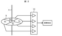
- the operator can add and subtract the detection signals of the detection elements of the backscattered electron detector to obtain images of various textures. For example, it is possible to obtain an image in which the unevenness information is emphasized by subtracting the detection signals of the opposing elements in each of the detection elements 9a to 9d in FIG. 2, but addition and subtraction operations of the detection signals are performed Every adjustment is necessary, operation is complicated, and it depends on the experience of the operator.
- the signal amount of positive ions is determined by the electric field strength of the bias electrode and the distance between the sample and the bias electrode, so by changing the voltage applied to this bias electrode Need to get the best image.
- the signal detection efficiency increases as the vacuum decreases because gas amplification by the residual gas in the sample chamber is used.
- the degree of vacuum decreases, the electron beam irradiated to the sample is scattered. The image quality is degraded below the vacuum level.
- the operation of optimizing the adjustment and acquiring the image every time the setting of the electric field strength of the bias electrode and the vacuum degree is performed is complicated and depends on the experience of the worker.
- an arbitrary observation condition setting of each detector is continuously changed, an image is displayed in real time, and an observer can display a desired image from among the continuously displayed images.
- the observation condition setting is automatically set, the observation condition desired by the operator can be easily set, and an image can be acquired.
- the observation condition has a working distance, and an image is displayed in real time while changing the working distance, and the operator selects an image at the time when the desired image is displayed, Observation conditions can be easily set and images can be acquired.
- the observation condition has a vacuum degree, and an image is displayed in real time while changing the vacuum degree, and the operator selects the image at the time when the desired image is displayed, Observation conditions can be easily set and images can be acquired.
- the observation condition includes addition / subtraction operation of each detection signal of the reflection electron detection element divided into plural, and displays images of various textures obtained by addition / subtraction of the signal of each detection element in real time
- the operator can easily set the viewing conditions and obtain the image by selecting the image when the desired image is displayed.
- FIG. 2 is a diagram showing a four-divided backscattered electron detection element.
- FIG. 7 is a view showing a sample image of a quadruple split reflection electron detection image in which asperity information is emphasized.
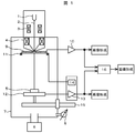
- FIG. 1 is a view showing a configuration example of a scanning electron microscope provided with a backscattered electron detector and a low vacuum secondary electron detector according to the present invention.
- the electron beam 2 generated from the electron gun 1 is focused by the focusing lens 3 and the objective lens 4 and irradiated to the sample 5 to generate reflected electrons and secondary electrons.
- the amount of air introduced into the sample chamber 7 is controlled by opening and closing the leak valve 8, and the degree of vacuum inside the sample chamber is adjusted.
- the backscattered electron detector detects the backscattered electrons generated by the irradiation of the sample 5 with the electron beam by the backscattered electron detection element 9 and amplifies the backscattered electrons by the backscattered electron detection amplifier 10 to form an image.
- the low vacuum secondary electron detector secondary electrons generated by irradiating the sample 5 with the electron beam 2 are accelerated toward the bias electrode 11 applied with a positive voltage, and the residual gas in the sample chamber is generated. The collision separates the residual gas into positive ions and electrons, and the generated electrons are similarly accelerated to the bias electrode 11 and collide with other residual gas molecules to be separated into positive ions and electrons. repeat.
- the generated positive ions drift in the direction of the sample by the bias electrode 11 and are absorbed by the sample stage 12.
- the absorbed current is detected and amplified by the low vacuum secondary electron detection amplifier 13 to form an image.
- the detection signals of the two detectors can be amplified by the respective amplifiers and then combined by the operational amplifier 16 to form a characteristic mixed image.
- the texture of the image changes depending on the observation conditions such as the working distance and the degree of vacuum, and the optimum observation conditions of the respective detectors are different. Furthermore, in the backscattered electron detector, the texture of the image is changed by adding / subtracting the detection signal of each divided detection element, and in the low vacuum secondary electron detector, the applied voltage of the bias electrode 11 is changed. The texture of the image changes. In addition, it has a function capable of displaying an image obtained by mixing two image signals, and by changing the mixing ratio of the signals, images of various textures can be displayed.
- the working distance is changed by the stage drive motor 15 to display an image in real time.
- the operator selects an image that is felt as optimal from the image displayed in real time when the image is displayed.
- the amount of air introduced into the sample chamber 7 is controlled by the opening / closing amount of the leak valve 8 to display an image in real time while changing the degree of vacuum inside the sample chamber.
- the operator selects an image at the time when the image which feels optimum is displayed from the images displayed in real time.
- images of various textures obtained by addition / subtraction of the signal of each detection element are displayed in real time. For example, in order to obtain an image emphasizing asperity information desired by the operator, first, the image 17 obtained from the detection signal from only the backscattered electron detection element 9a is displayed, and then the backscattered electron detection element 9a And 9b, and then the image 19 obtained from the detection signal from only the backscattered electron detection element 9b is displayed. Similarly, the images 21 and 9c from 9b and 9c and the images 22 and 9c from 9c and 9d and the images 23 and 9d and 9a and 24 are displayed in this order. It is an image which displays continuously the image which observed the sample 5 sequentially, illuminating and shadowing the sample 5 from upper eight directions. The operator selects an image from the continuously displayed images when an image which feels optimum is displayed.
- an image is displayed in real time while controlling the high voltage power supply 14 to change the voltage.
- the operator selects an image at the time when the image which feels optimum is displayed from the images displayed in real time.
- the image is displayed in real time while continuously changing the mixing ratio of the signals synthesized by the operational amplifier 16.
- the operator selects an image at the time when the image which feels optimum is displayed from the images displayed in real time. For example, the mixing ratio is continuously changed from 0 to 100, the image is displayed in real time, and it is possible to select the image at the time when the image which seems to be the operator optimum is displayed.
- the present invention can be applied to other detectors such as a high vacuum secondary electron detector and transmitted electrons by a scintillator or the like.
- the present invention can also be applied to the determination of the acceleration voltage, the excitation condition of the condenser lens, and the like under observation conditions.
Landscapes
- Chemical & Material Sciences (AREA)
- Analytical Chemistry (AREA)
- Engineering & Computer Science (AREA)
- Computer Vision & Pattern Recognition (AREA)
- Analysing Materials By The Use Of Radiation (AREA)
Abstract
本発明の目的は、異なる種類の複数の検出器を有した走査電子顕微鏡において、任意の観察条件で操作者が所望する観察画像を容易に取得する手段を提供することにある。 前記目的を達成するために、任意の観察条件を連続的に変化させながら画像をリアルタイムに表示させ、操作者はリアルタイムに表示される画像から、最適と感じる画像を選択することで容易に画像を取得することができる。観察条件には、ワーキングディスタンス,真空度,複数に分割された反射電子検出素子の検出信号の加減算操作、低真空二次電子検出器のバイアス電極に印加する電圧、ミキシング画像を表示する際の信号の混合比がある。
Description
本発明は、走査電子顕微鏡に関し、特に観察条件の選択方法に関する。
走査電子顕微鏡は、一般に試料に電子ビームを照射し、試料から放出される二次電子、または反射電子を検出器によって検出し像を形成する。二次電子は試料表面近くから発生する電子で、形成される二次電子像は試料の凹凸を反映する。反射電子は試料を構成している原子に当って跳ね返された電子で、その数は試料の組成に依存するため、反射電子像は試料表面の組成成分を反映した像となる。また、低真空観察機能を有する走査電子顕微鏡は、1Pa以下の高真空時に主に使用する二次電子検出器の他に、1Pa以上の低真空時では、反射電子検出器の他に、残留ガス分子による二次電子増幅作用を利用した低真空二次電子検出器などがある。
反射電子像を観察する場合、試料で後方散乱される反射電子を反射電子検出器によって検出する。反射電子検出器には、反射電子の検出面が複数に分割されているものがあり、例えば四分割検出器の場合には、4つの検出面に設けられた各検出素子から検出した信号に対して加算,減算などの演算処理が施され画像形成される。
なお反射電子は、試料表面の凹凸により電子ビームの試料への入射角に対し鏡面反射方向を主とする分布で発生し、反射電子検出器の各素子で検出される。通常観察では、これらの全ての検出面の検出素子の出力信号を加算して画像を形成するが、対向する素子の出力信号を減算することで、試料の凹凸情報を強調した画像を観察することができる装置が普及している。
少なくとも2つ以上の検出器を有する走査電子顕微鏡を用いて画像観察を行う場合、操作者が所望する画像を取得するためには、まず使用する検出器を決定し、その検出器に応じて、加速電圧,ワーキングディスタンス,真空度などを設定する必要がある。そのため、操作者が観察条件を変化させて所望する画像が取得できる条件を目視で確認しながら決定せねばならず、操作が煩雑であり操作者の経験に依存する。
たとえば、理論的にはワーキングディスタンスは短い方がよいが、反射電子検出器では、電子ビーム近傍に鏡面反射する反射電子は短いワーキングディスタンスでは検出器の電子ビーム通路から上方に抜けてしまい検出効率が落ちるため、最適なワーキングディスタンスの設定は、経験的に決まる。また、操作者が反射電子検出器の各検出素子の検出信号を加減算して、様々な質感の画像を取得することが可能である。たとえば、図2の9aから9dまでの各検出素子で、対向する素子の検出信号を減算することにより、凹凸情報を強調した画像を取得することが可能であるが、検出信号の加減算操作をする毎に調整を必要とし、操作が煩雑であり、操作者の経験に依存する。
低真空二次電子検出器の観察では、プラスイオンの信号量は、バイアス電極の電界強度と、試料とバイアス電極との距離で決定されるため、このバイアス電極に印加する電圧を変化させることにより、最適な画像を取得する必要がある。また、試料室中の残留ガスによるガス増幅を利用しているため、低真空になるほど信号検出効率が増すが、真空度が低下するに従い、試料に照射される電子ビームが散乱するため、ある程度の真空度以下では画質が低下する。このように、バイアス電極の電界強度や、真空度の設定をする毎に調整を最適にして画像を取得する作業は煩雑であり、作業者の経験に依存する。
また、反射電子像と低真空二次電子像の2つの信号を同時に検出し、演算増幅器16で合成することにより、特徴のあるミキシング画像を形成することができるが、この信号の混合比の決定には、混合比を設定する毎に操作者が目視確認をしながら決定せねばならず、操作が煩雑となる。
本発明の目的は、複数の検出器を有する走査電子顕微鏡において、任意の観察条件を自動的に連続変化させながら、その観察像をリアルタイムで表示することにより、最適な観察条件設定を簡単にできる走査電子顕微鏡を提供することにある。
(1)上記目的を達成するために、各検出器の任意の観察条件設定を連続的に変化させていき、画像をリアルタイムに表示させ、観察者は連続表示される画像の中から所望の画像を選択することで、その観察条件設定に自動設定され、容易に操作者の所望する観察条件を設定し、画像が取得できることを特徴とする。
(2)上記(1)において、観察条件にはワーキングディスタンスがあり、ワーキングディスタンスを変化させながら画像をリアルタイムに表示させ、操作者は所望する画像が表示された時点の画像を選択することで、容易に観察条件設定,画像取得が可能となる。
(3)上記(1)において、観察条件には真空度があり、真空度を変化させながら画像をリアルタイムに表示させ、操作者は所望する画像が表示された時点の画像を選択することで、容易に観察条件設定,画像取得が可能となる。
(4)上記(1)において、観察条件には複数に分割された反射電子検出素子の各検出信号の加減算操作があり、各検出素子の信号を加減算させた様々な質感の画像をリアルタイムに表示させ、操作者は所望する画像が表示された時点の画像を選択することで、容易に観察条件設定,画像取得が可能となる。
(5)上記(1)において、観察条件にはバイアス電極に印加する電圧があり、印加電圧を変化させながら画像をリアルタイムに表示させ、操作者は所望する画像が表示された時点の画像を選択することにより、容易に観察条件設定,画像取得が可能となる。
(6)上記(1)において、観察条件にはミキシング画像を形成する際、2つの信号の混合比があり、信号の混合比率を連続的に変化させながらミキシング画像をリアルタイムに表示させ、操作者は所望する画像が表示された時点の画像を選択することにより、容易に観察条件設定,画像取得が可能となる。
本発明により、煩雑な操作をせず、また、操作者の経験に依存することなく容易に操作者が所望する観察条件設定,画像を取得することができる。
以下、図面を用いて本発明の実施形態を説明する。
図1は本発明に係わる反射電子検出器と低真空二次電子検出器を備えた走査電子顕微鏡の構成例を示す図である。
図1は本発明に係わる反射電子検出器と低真空二次電子検出器を備えた走査電子顕微鏡の構成例を示す図である。
低真空において二次電子像を観察する場合、バイアス電極11に正電圧を印加し、電極と試料間に電界を発生させ、この電界により試料から発生する二次電子を電極方向に加速する。加速された二次電子は残留ガス分子に衝突し、残留ガス分子が電子とプラスイオンに分離される。この過程が繰り返されることによる増幅現象を利用し、プラスイオンをバイアス電極により試料方向にドリフトさせ、試料に吸収されたプラスイオンに起因して発生する吸収電流を検出して画像を形成する。
電子銃1から発生した電子ビーム2は、集束レンズ3および対物レンズ4で集束され試料5に照射され、反射電子や二次電子が発生する。低真空の設定は、排気装置6によって試料室7を真空排気しながら、リークバルブ8の開閉により試料室7へのエアー導入量を制御し、試料室内部の真空度を調整する。
反射電子検出器は、試料5に電子ビームが照射されることにより発生した反射電子を、反射電子検出素子9で検出し、反射電子検出増幅器10で増幅させ画像形成する。低真空二次電子検出器は、試料5に電子ビーム2が照射されることにより発生した二次電子が、正電圧に印加されたバイアス電極11に向かって加速され、試料室内部の残留ガスに衝突することで残留ガスがプラスイオンと電子に分離し、この発生した電子も同様にバイアス電極11に加速され、更に別の残留ガス分子に衝突することでプラスイオンと電子に分離させ、この現象を繰り返す。発生したプラスイオンはバイアス電極11により試料方向にドリフトして試料台12に吸収され、この吸収電流を検出して低真空二次電子検出増幅器13で増幅し、画像形成する。上記2つの検出器の検出信号は、各々増幅器で増幅された後、演算増幅器16で合成することにより特徴のあるミキシング画像を形成することができる。
上記2つの検出器による観察画像は、ワーキングディスタンス,真空度といった観察条件により画像の質感が変化し、各検出器の最適な観察条件はそれぞれ異なる。更に、反射電子検出器では、分割された検出素子毎の検出信号の加減算をすることにより画像の質感が変化し、低真空二次電子検出器では、バイアス電極11の印加電圧を変化させることで画像の質感が変化する。また、2つの画像信号をミックスした画像を表示できる機能を備え、その信号の混合比を変化させることで、様々な質感の画像を表示させることができる。
観察条件でワーキングディスタンスを決定する場合、ステージ駆動モータ15によりワーキングディスタンスを変化させ、リアルタイムに画像を表示させる。操作者は、リアルタイムに表示される画像から、最適と感じる画像が表示された時点でその画像を選択する。
観察条件で真空度を決定する場合、リークバルブ8の開閉量によって試料室7への空気導入量を制御し、試料室内部の真空度を変化させながら、リアルタイムに画像を表示させる。操作者は、リアルタイムに表示される画像から、最適と感じる画像が表示された時点での画像を選択する。
観察条件で、複数に分割された反射電子検出素子9の各検出信号の加減算操作を決定する場合、各検出素子の信号を加減算させた様々な質感の画像をリアルタイムに表示させる。たとえば、操作者が所望する凹凸情報を強調した画像を取得するためには、まず初めに、反射電子検出素子9aのみからの検出信号より得られる画像17を表示させ、次に反射電子検出素子9aと9bからの検出信号より得られる画像18を表示させ、次に反射電子検出素子9bのみからの検出信号より得られる画像19を表示させる。以下同様に9bと9cからの画像20、9cのみからの画像21、9cと9dからの画像22、9dのみからの画像23、9dと9aからの画像24という順番で表示させる。試料5を上方8方向から順に照明を当てて影をつけながら観察したような画像を連続表示するイメージである。操作者は、この連続表示される画像から、最適と感じる画像が表示された時点でその画像を選択する。
観察条件でバイアス電極11に印加する電圧を決定する場合、高電圧電源14を制御し電圧を変化させながら、リアルタイムに画像を表示させる。操作者は、リアルタイムに表示される画像から、最適と感じる画像が表示された時点での画像を選択する。
観察条件で、2つの画像信号の混合比を決定する場合、演算増幅器16で合成する信号の混合比を連続的に変化させながら、リアルタイムで画像を表示させる。操作者は、リアルタイムに表示される画像から、最適と感じる画像が表示された時点での画像を選択する。たとえば、混合比率0から100まで連続に変化させることを繰り返し、画像をリアルタイムに表示させ、操作者最適と感じられる画像が表示された時点の画像を選択可能とする。
以上説明では、反射電子検出器,低真空二次電子検出器に関して説明したが、高真空二次電子検出器や、シンチレータ等による透過電子等、他の検出器においても適用できる。また、観察条件においても、加速電圧や、コンデンサレンズの励磁条件等の決定にも適用できる。
以上説明したように、任意の観察条件を連続的に変化させながら画像をリアルタイムに表示させ、操作者は表示される画像から最適と感じる画像を選択することにより容易に画像取得することが可能となる。
1 電子銃
2 電子ビーム
3 集束レンズ
4 対物レンズ
5 試料
6 排気装置
7 試料室
8 リークバルブ
9 反射電子検出素子
10 反射電子検出増幅器
11 バイアス電極
12 試料台
13 低真空二次電子検出増幅器
14 高電圧電源
15 ステージ駆動モータ
16 演算増幅器
17 9a検出信号を強調した画像
18 9aと9b検出信号を強調した画像
19 9b検出信号を強調した画像
20 9bと9c検出信号を強調した画像
21 9c検出信号を強調した画像
22 9cと9d検出信号を強調した画像
23 9d検出信号を強調した画像
24 9dと9a検出信号を強調した画像
2 電子ビーム
3 集束レンズ
4 対物レンズ
5 試料
6 排気装置
7 試料室
8 リークバルブ
9 反射電子検出素子
10 反射電子検出増幅器
11 バイアス電極
12 試料台
13 低真空二次電子検出増幅器
14 高電圧電源
15 ステージ駆動モータ
16 演算増幅器
17 9a検出信号を強調した画像
18 9aと9b検出信号を強調した画像
19 9b検出信号を強調した画像
20 9bと9c検出信号を強調した画像
21 9c検出信号を強調した画像
22 9cと9d検出信号を強調した画像
23 9d検出信号を強調した画像
24 9dと9a検出信号を強調した画像
Claims (10)
- 異なる種類の複数の検出器を有した走査電子顕微鏡であって、任意の観察条件を連続的に変化させながら、リアルタイムに画像を表示させ、操作者はその表示される画像を選択することで所望する画像を容易に取得することができることを特徴とする走査電子顕微鏡。
- 請求項1の走査電子顕微鏡において、観察条件にはワーキングディスタンスがあり、ワーキングディスタンスを変化させながら画像をリアルタイムに表示させ、操作者に所望する画像を選択させることを特徴とする走査電子顕微鏡。
- 請求項1の走査電子顕微鏡において、観察条件には真空度があり、真空度を変化させながら画像をリアルタイムに表示させ、操作者に所望する画像を選択させることを特徴とする走査電子顕微鏡。
- 請求項3の走査電子顕微鏡において、画像選択時の真空度設定値ではなく、選択された画像が形成された時点の真空度を測定し、その値を観察条件にできることを特徴とする走査電子顕微鏡。
- 請求項1の走査電子顕微鏡において、観察条件には複数に分割された反射電子検出素子の各検出信号の加減算操作があり、各検出素子の信号を加減算させた様々な質感の画像をリアルタイムに表示させ、操作者に所望する画像を選択させることを特徴とする走査電子顕微鏡。
- 請求項1の走査電子顕微鏡において、観察条件には低真空二次電子検出器のバイアス電極に印加する電圧があり、印加電圧を変化させながら画像をリアルタイムに表示させ、操作者に所望する画像を選択させることを特徴とする走査電子顕微鏡。
- 請求項1の走査電子顕微鏡において、観察条件のパラメータとし、パラメータの連続的変化を繰り返し行うことができることを特徴とする走査電子顕微鏡。
- 請求項7の走査電子顕微鏡において、パラメータを変化するスピードを可変できることを特徴とする走査電子顕微鏡。
- 走査電子顕微鏡において、画像がある所望する輝度に達したらその時の設定条件を選択できることを特徴とする走査電子顕微鏡。
- 請求項9の走査電子顕微鏡において、その所望する輝度に達するまでの時間を測定できることを特徴とする走査電子顕微鏡。
Applications Claiming Priority (2)
| Application Number | Priority Date | Filing Date | Title |
|---|---|---|---|
| JP2011-104831 | 2011-05-10 | ||
| JP2011104831A JP2012238400A (ja) | 2011-05-10 | 2011-05-10 | 電子顕微鏡 |
Publications (1)
| Publication Number | Publication Date |
|---|---|
| WO2012153449A1 true WO2012153449A1 (ja) | 2012-11-15 |
Family
ID=47138943
Family Applications (1)
| Application Number | Title | Priority Date | Filing Date |
|---|---|---|---|
| PCT/JP2012/001748 Ceased WO2012153449A1 (ja) | 2011-05-10 | 2012-03-14 | 電子顕微鏡 |
Country Status (2)
| Country | Link |
|---|---|
| JP (1) | JP2012238400A (ja) |
| WO (1) | WO2012153449A1 (ja) |
Cited By (1)
| Publication number | Priority date | Publication date | Assignee | Title |
|---|---|---|---|---|
| CN105593966A (zh) * | 2013-10-08 | 2016-05-18 | 株式会社日立高新技术 | 带电粒子束装置、带电粒子束装置的控制方法 |
Families Citing this family (1)
| Publication number | Priority date | Publication date | Assignee | Title |
|---|---|---|---|---|
| JP2022185769A (ja) | 2021-06-03 | 2022-12-15 | 日本電子株式会社 | 走査型電子顕微鏡、及び、走査型電子顕微鏡を用いた画像生成方法 |
Citations (3)
| Publication number | Priority date | Publication date | Assignee | Title |
|---|---|---|---|---|
| JP2005004995A (ja) * | 2003-06-09 | 2005-01-06 | Hitachi High-Technologies Corp | 走査形電子顕微鏡 |
| JP2006190554A (ja) * | 2005-01-06 | 2006-07-20 | Jeol Ltd | 電子顕微鏡における複数信号の画像調整法と装置 |
| WO2010084860A1 (ja) * | 2009-01-22 | 2010-07-29 | 株式会社日立ハイテクノロジーズ | 電子顕微鏡 |
-
2011
- 2011-05-10 JP JP2011104831A patent/JP2012238400A/ja not_active Withdrawn
-
2012
- 2012-03-14 WO PCT/JP2012/001748 patent/WO2012153449A1/ja not_active Ceased
Patent Citations (3)
| Publication number | Priority date | Publication date | Assignee | Title |
|---|---|---|---|---|
| JP2005004995A (ja) * | 2003-06-09 | 2005-01-06 | Hitachi High-Technologies Corp | 走査形電子顕微鏡 |
| JP2006190554A (ja) * | 2005-01-06 | 2006-07-20 | Jeol Ltd | 電子顕微鏡における複数信号の画像調整法と装置 |
| WO2010084860A1 (ja) * | 2009-01-22 | 2010-07-29 | 株式会社日立ハイテクノロジーズ | 電子顕微鏡 |
Cited By (2)
| Publication number | Priority date | Publication date | Assignee | Title |
|---|---|---|---|---|
| CN105593966A (zh) * | 2013-10-08 | 2016-05-18 | 株式会社日立高新技术 | 带电粒子束装置、带电粒子束装置的控制方法 |
| CN105593966B (zh) * | 2013-10-08 | 2017-05-24 | 株式会社日立高新技术 | 带电粒子束装置、带电粒子束装置的控制方法 |
Also Published As
| Publication number | Publication date |
|---|---|
| JP2012238400A (ja) | 2012-12-06 |
Similar Documents
| Publication | Publication Date | Title |
|---|---|---|
| JP5372020B2 (ja) | 電子顕微鏡 | |
| US8969801B2 (en) | Scanning electron microscope | |
| JP6014688B2 (ja) | 複合荷電粒子線装置 | |
| JP5584159B2 (ja) | 荷電粒子線装置及びパターン測定方法 | |
| JP5183318B2 (ja) | 荷電粒子線装置 | |
| JP2011159483A (ja) | 電子顕微鏡及び試料分析方法 | |
| EP3506332A1 (en) | Charged particle beam device and analysis method | |
| JP7018365B2 (ja) | 荷電粒子線装置および分析方法 | |
| JP2017198657A (ja) | 荷電粒子顕微鏡における3次元イメージング | |
| JP2015184040A (ja) | エネルギー分散型x線分析装置及びエネルギー分散型x線分析方法 | |
| US10720304B2 (en) | Charged particle beam apparatus and image acquisition method | |
| JP6343508B2 (ja) | コントラスト・ブライトネス調整方法、及び荷電粒子線装置 | |
| JP7323574B2 (ja) | 荷電粒子線装置および画像取得方法 | |
| JP2013196972A (ja) | 試料観察方法、試料作製方法及び荷電粒子ビーム装置 | |
| JP2020194691A (ja) | 電子顕微鏡における試料観察方法、電子顕微鏡用画像解析装置、電子顕微鏡および電子顕微鏡用画像解析方法 | |
| JP6215557B2 (ja) | 電子顕微鏡 | |
| JP6266467B2 (ja) | 電子顕微鏡、およびモノクロメーターの調整方法 | |
| JP2012238400A (ja) | 電子顕微鏡 | |
| JP5248128B2 (ja) | 画像信号処理方法及び装置、並びに荷電粒子線装置 | |
| JP2023007094A (ja) | 走査電子顕微鏡 | |
| JP4045470B2 (ja) | コンフォーカル顕微鏡 | |
| WO2015045443A1 (ja) | 電子顕微鏡 | |
| JP2014212063A (ja) | 走査荷電粒子顕微鏡、走査荷電粒子顕微鏡の制御方法、および走査荷電粒子顕微鏡の軸合わせ方法 | |
| KR20110120684A (ko) | 노이즈 제거 효과가 향상된 주사 전자 현미경 및 그 제어방법 | |
| JP5500868B2 (ja) | 走査電子顕微鏡、および走査電子顕微鏡における像表示方法 |
Legal Events
| Date | Code | Title | Description |
|---|---|---|---|
| 121 | Ep: the epo has been informed by wipo that ep was designated in this application |
Ref document number: 12782159 Country of ref document: EP Kind code of ref document: A1 |
|
| NENP | Non-entry into the national phase |
Ref country code: DE |
|
| 122 | Ep: pct application non-entry in european phase |
Ref document number: 12782159 Country of ref document: EP Kind code of ref document: A1 |