WO2012153407A1 - 照明装置 - Google Patents
照明装置 Download PDFInfo
- Publication number
- WO2012153407A1 WO2012153407A1 PCT/JP2011/060874 JP2011060874W WO2012153407A1 WO 2012153407 A1 WO2012153407 A1 WO 2012153407A1 JP 2011060874 W JP2011060874 W JP 2011060874W WO 2012153407 A1 WO2012153407 A1 WO 2012153407A1
- Authority
- WO
- WIPO (PCT)
- Prior art keywords
- panel
- organic
- bis
- hole
- layer
- Prior art date
- Legal status (The legal status is an assumption and is not a legal conclusion. Google has not performed a legal analysis and makes no representation as to the accuracy of the status listed.)
- Ceased
Links
Images




Classifications
-
- F—MECHANICAL ENGINEERING; LIGHTING; HEATING; WEAPONS; BLASTING
- F21—LIGHTING
- F21S—NON-PORTABLE LIGHTING DEVICES; SYSTEMS THEREOF; VEHICLE LIGHTING DEVICES SPECIALLY ADAPTED FOR VEHICLE EXTERIORS
- F21S8/00—Lighting devices intended for fixed installation
- F21S8/04—Lighting devices intended for fixed installation intended only for mounting on a ceiling or the like overhead structures
-
- F—MECHANICAL ENGINEERING; LIGHTING; HEATING; WEAPONS; BLASTING
- F21—LIGHTING
- F21V—FUNCTIONAL FEATURES OR DETAILS OF LIGHTING DEVICES OR SYSTEMS THEREOF; STRUCTURAL COMBINATIONS OF LIGHTING DEVICES WITH OTHER ARTICLES, NOT OTHERWISE PROVIDED FOR
- F21V29/00—Protecting lighting devices from thermal damage; Cooling or heating arrangements specially adapted for lighting devices or systems
- F21V29/50—Cooling arrangements
- F21V29/70—Cooling arrangements characterised by passive heat-dissipating elements, e.g. heat-sinks
- F21V29/83—Cooling arrangements characterised by passive heat-dissipating elements, e.g. heat-sinks the elements having apertures, ducts or channels, e.g. heat radiation holes
-
- F—MECHANICAL ENGINEERING; LIGHTING; HEATING; WEAPONS; BLASTING
- F21—LIGHTING
- F21V—FUNCTIONAL FEATURES OR DETAILS OF LIGHTING DEVICES OR SYSTEMS THEREOF; STRUCTURAL COMBINATIONS OF LIGHTING DEVICES WITH OTHER ARTICLES, NOT OTHERWISE PROVIDED FOR
- F21V33/00—Structural combinations of lighting devices with other articles, not otherwise provided for
- F21V33/0088—Ventilating systems
-
- F—MECHANICAL ENGINEERING; LIGHTING; HEATING; WEAPONS; BLASTING
- F24—HEATING; RANGES; VENTILATING
- F24F—AIR-CONDITIONING; AIR-HUMIDIFICATION; VENTILATION; USE OF AIR CURRENTS FOR SCREENING
- F24F13/00—Details common to, or for air-conditioning, air-humidification, ventilation or use of air currents for screening
- F24F13/02—Ducting arrangements
- F24F13/06—Outlets for directing or distributing air into rooms or spaces, e.g. ceiling air diffuser
- F24F13/078—Outlets for directing or distributing air into rooms or spaces, e.g. ceiling air diffuser combined with lighting fixtures
-
- H—ELECTRICITY
- H10—SEMICONDUCTOR DEVICES; ELECTRIC SOLID-STATE DEVICES NOT OTHERWISE PROVIDED FOR
- H10K—ORGANIC ELECTRIC SOLID-STATE DEVICES
- H10K50/00—Organic light-emitting devices
- H10K50/80—Constructional details
- H10K50/87—Arrangements for heating or cooling
-
- H—ELECTRICITY
- H10—SEMICONDUCTOR DEVICES; ELECTRIC SOLID-STATE DEVICES NOT OTHERWISE PROVIDED FOR
- H10K—ORGANIC ELECTRIC SOLID-STATE DEVICES
- H10K59/00—Integrated devices, or assemblies of multiple devices, comprising at least one organic light-emitting element covered by group H10K50/00
- H10K59/80—Constructional details
- H10K59/8794—Arrangements for heating and cooling
-
- F—MECHANICAL ENGINEERING; LIGHTING; HEATING; WEAPONS; BLASTING
- F21—LIGHTING
- F21Y—INDEXING SCHEME ASSOCIATED WITH SUBCLASSES F21K, F21L, F21S and F21V, RELATING TO THE FORM OR THE KIND OF THE LIGHT SOURCES OR OF THE COLOUR OF THE LIGHT EMITTED
- F21Y2105/00—Planar light sources
-
- F—MECHANICAL ENGINEERING; LIGHTING; HEATING; WEAPONS; BLASTING
- F21—LIGHTING
- F21Y—INDEXING SCHEME ASSOCIATED WITH SUBCLASSES F21K, F21L, F21S and F21V, RELATING TO THE FORM OR THE KIND OF THE LIGHT SOURCES OR OF THE COLOUR OF THE LIGHT EMITTED
- F21Y2115/00—Light-generating elements of semiconductor light sources
- F21Y2115/20—Electroluminescent [EL] light sources
Definitions
- the present invention relates to a lighting device using an electroluminescence panel.
- organic electroluminescence element As an electroluminescence panel, an organic compound having charge transportability (hole or electron mobility), which has achieved higher luminance and higher luminous efficiency than inorganic electroluminescence elements (hereinafter referred to as inorganic EL elements), has been used.
- An organic electroluminescence element (hereinafter referred to as an organic EL element) provided with a plurality of organic material layers has attracted attention.
- Organic EL elements as flexible thin surface light sources are rapidly put into practical use in the fields of mobile phones, car navigation systems, and TV displays, and are applied to special lighting such as endoscopes. Further, LEDs as point light sources are also increasingly applied to lighting devices.
- a blower outlet integrated LED lighting device in which a thin LED lighting device is fixed to a frame of an air conditioning suction port or a blower outlet to form a rectangular air conditioning suction port or blower device as a whole (Patent Document 1). ,reference).
- the organic EL element the EL is provided so as to surround the opening (air duct or water duct) provided in the handpiece head for attaching / detaching a medical tool or for taking out or entering a work medium.
- Patent Document 2 A medical device for dentistry provided with a surface emitting light source of an element has been proposed (refer to Patent Document 2), an illuminating means for an organic EL element, a light receiving portion, and a through-hole for inserting a treatment instrument
- An endoscope tip is proposed in which the illumination means is formed so as to avoid the light receiving portion and the through hole (having an opening at the light receiving portion and the through hole)
- Patent Document 3 And a surface emitting device for a ceramic filter in which a plurality of through holes serving as a fluid flow path are formed in a direction perpendicular to the surface of a surface light emitter having a function of emitting ultraviolet rays (Patent Document). 4)) for special lighting fields It has been applied.
- clean rooms that remove dust are used to improve the quality of precision products for applications such as electronics, precision machinery, and precision printing, and improve yields.
- the outer surface of the glass tube of a fluorescent lamp is covered with a yellow tube to absorb light having a wavelength of 500 nm or less and ultraviolet rays. For this reason, the interior of the clean room is yellow.
- the lighting device and the blower are separate devices, and it is desirable to integrate them in order to effectively use the ceiling space.
- a clean room lighting device only a part of the light that can be used by covering the yellow tube is used, and the light use efficiency deteriorates.
- conventional fluorescent lamps, light bulbs and the like cannot provide a ventilation hole on the light emitting surface, so the cooling efficiency of the light emitting unit is low, and the light emitting unit and the air blowing unit become different devices and take up space.
- Patent Documents 1 to 4 do not use ultraviolet rays and are not considered for effective use of space and improvement of cooling efficiency.
- An illuminating device is an illuminating device including a surface light emitter and a housing that defines an internal space by a partition including the surface light emitter, and the surface light emitter has a transmissive substrate and is visible.
- An electroluminescence panel that emits light in a planar shape, wherein the electroluminescence panel has a plurality of through holes penetrating from the internal space to the outside.
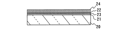
- FIG. 3 is a sectional view taken along line AA in FIG. 2.
- FIG. 3 is a sectional view taken along line BB in FIG. 2.
- schematic fragmentary sectional view which shows the organic EL element of embodiment by this invention.
- schematic partially notched perspective view which shows the illumination panel with a ventilation hole which is the illuminating device of other embodiment by this invention.
- FIG. 1 shows an illumination panel device 1 with an air blowing hole of this embodiment using an organic EL panel as an electroluminescence panel.
- a plate-shaped organic EL panel 2 which is a surface light emitter is used.
- the organic EL panel 2 is provided with a plurality of through holes 4 formed on the surface thereof and penetrating from the internal space to the outside.
- the lighting panel device 1 with a ventilation hole includes a housing 5 that defines an internal space by a partition including an organic EL panel 2.
- Air 3 from a blower (not shown) is supplied to the housing 5 through the conduit 6, and air is blown from the through holes 4.
- the outer surface of the organic EL panel 2 other than the through holes 4 emits light and is used as illumination.
- a dust air filter F such as a high efficiency particulate air (HEPA) filter or an ultra low penetration air (ULPA) filter may be provided in the internal space of the housing 5 so as to face the through hole 4 in parallel. it can.
- HEPA high efficiency particulate air
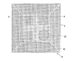
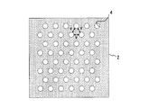
- FIG. 2 is a schematic partial plan view showing the organic EL panel 2 of the lighting panel with air holes of the present embodiment.
- 3 is a cross-sectional view taken along line AA in FIG. 4 in FIG. 2
- FIG. 4 is a cross-sectional view taken along line BB in FIG.
- the surface-emitting organic EL panel 2 includes a transmissive substrate 20, a transmissive first electrode 21, and a light-reflective second electrode 22 formed thereon. It has a plurality of organic material layers 23 including a light emitting layer of at least one kind of light emitting color disposed between them.
- the substrate 20 supports the first electrode 21 and emits visible light in a planar shape from the substrate 20 side.
- the embodiment according to the present invention is a lighting device including the organic EL panel 2 and the housing 5 that defines the internal space by the partition including the organic EL panel 2.
- a protective layer 24 is provided on the second electrode 22 side, and the organic EL panel 2 is formed in a laminated structure. As shown in FIG. 4, the inner wall surfaces of the through holes 4 of the organic EL panel 2 are all protected by a protective film P such as a moisture barrier film.
- Organic EL panel As shown in FIG. 5, on a transparent substrate 20 such as glass, a transparent anode 21 (first electrode), a hole injection layer 33, a hole transport layer 34, a light emitting layer 35, and a hole blocking layer 36 are sequentially formed. , An electron transport layer 37, an electron injection layer 38, and a cathode (second electrode) 22 made of metal are stacked.
- the hole injection layer 33, the hole transport layer 34, the light emitting layer 35, the hole blocking layer 36, and the electron transport layer 37 are the organic material layer 23.
- each organic EL element of the organic EL panel is an organic EL element provided with a plurality of organic material layers including a light emitting layer, which are stacked between a pair of opposed anodes and cathodes.
- any organic material layer such as a light emitting layer, a hole injection layer, and a hole transport layer can be formed by a dry film forming method such as a vacuum evaporation method or a wet coating method such as an ink jet method.
- the separator of each layer shown in FIG. 5 is represented by “/”, and anode 21 / hole injection layer 33 / hole transport layer 34 / light emitting layer 35 / hole blocking layer 36 / electron transport layer 37 / electron injection
- the anode 21 / hole injection layer 33 / light emitting layer 35 / electron transport layer 37 / electron injection layer 38 / cathode 22 / hole transport layer 34 positive
- the hole blocking layer 36 is omitted, and although not shown, the anode 21 / hole transport layer 34 / light emitting layer 35 / electron transport layer 37 / electron injection layer 38 / cathode 22 / hole injection layer 33, hole blocking
- the present invention is not limited to these stacked structures, and includes a structure including at least a light-emitting layer or a charge transport layer that can also be used.
- a quartz or glass plate, a metal plate or a metal foil, a resin substrate to be bent, a plastic film, a sheet, or the like is used.
- a glass plate or a transparent synthetic resin plate such as polyester, polymethacrylate, polycarbonate, or polysulfone is preferable.
- a synthetic resin substrate it is necessary to pay attention to gas barrier properties. If the gas barrier property of the substrate is too small, the organic EL element may be deteriorated by the outside air that has passed through the substrate. For this reason, a method of providing a gas barrier property by providing a dense silicon oxide film or the like on at least one surface of the synthetic resin substrate is also a preferable method.
- the anode 21 that supplies holes to the layers up to the light emitting layer is usually a metal such as aluminum, gold, silver, nickel, palladium, platinum, or a metal such as indium and / or tin, zinc oxide (ITO or IZO). It is composed of an oxide, a metal halide such as copper iodide, carbon black, or a conductive polymer such as poly (3-methylthiophene), polypyrrole, or polyaniline.
- the anode is usually formed by a sputtering method, a vacuum deposition method, or the like.
- an appropriate binder resin solution is used.
- the anode can also be formed by dispersing and coating the substrate.
- a conductive polymer a thin film can be directly formed on the substrate by electrolytic polymerization, or the anode can be formed by applying a conductive polymer on the substrate.
- the anode usually has a single-layer structure, but it can also have a laminated structure made of a plurality of materials if desired.
- the thickness of the anode depends on the required transparency. When transparency is required, the visible light transmittance is usually 60% or more, preferably 80% or more. In this case, the thickness of the anode is usually 5 nm or more, preferably 10 nm or more, and is usually 1000 nm or less, preferably about 500 nm or less. If it may be opaque, the thickness of the anode is arbitrary, and the anode may be integrated with the substrate 20. Furthermore, different conductive materials may be laminated.
- the anode surface is subjected to ultraviolet (UV) treatment or ozone treatment, oxygen plasma or argon plasma surface treatment, etc. It is preferable to do.
- UV ultraviolet
- ozone treatment oxygen plasma or argon plasma surface treatment, etc. It is preferable to do.
- a material used for the cathode 22 for supplying electrons to the layers up to the light emitting layer a material used for the anode can be used.
- a metal having a low work function is preferable.
- a suitable metal such as tin, magnesium, indium, calcium, aluminum, silver, or an alloy thereof is used.
- Specific examples include low work function alloy electrodes such as magnesium-silver alloy, magnesium-indium alloy, and aluminum-lithium alloy.
- the material of the cathode 22 may use only 1 type, and may use 2 or more types together by arbitrary combinations and a ratio.
- the thickness of the cathode is usually the same as that of the anode.
- a metal layer having a high work function and stable to the atmosphere because the stability of the device is increased.
- metals such as aluminum, silver, copper, nickel, chromium, gold, platinum are used.
- these materials may be used only by 1 type and may use 2 or more types together by arbitrary combinations and a ratio.
- the material and film thickness are selected so as to be transparent or translucent.
- the material and film thickness are selected so as to be transparent or translucent.
- Organic material layer constituting the main components of the hole injection layer 33, the hole transport layer 34, the light emitting layer 35, the electron transport layer 36 and the electron injection layer 37 has a charge transport property (hole and / or electron mobility).
- Examples of phosphorescent organometallic complex compounds used for the light-emitting layer 35 include Bis (3,5-difluoro-2- (2-pyridyl) phenyl- (2-carboxypyridyl) iridium III, Tris (2-phenylpyridine) which are iridium complexes.
- Iridium (III) (Ir (ppy) 3), Bis (2-phenylbenzothiazolato) (acetylacetonate) iridium (III), Osmium (II) bis (3-trifluoromethyl -5- (2-pyridyl)- pyrazolate) dimethylphenylphosphine, rare earth compound Tris (dibenzoylmethane) phenanthroline europium (III), platinum complexes 2,3,7,8,12,13,17,18-Octaethyl-21H, 23H- porphine, platinum (II), etc.
- the light emitting layer 35 may include at least one kind of light emitting layer, and may be a mixed light emitting color or a multi-layered light emitting layer.
- Examples of the organic compound having an electron transporting property as a main component of the light emitting layer and the electron injection layer include polycyclic compounds such as p-terphenyl and quaterphenyl and derivatives thereof, naphthalene, tetracene, pyrene, coronene, chrysene, Condensed polycyclic hydrocarbon compounds such as anthracene, diphenylanthracene, naphthacene, phenanthrene and their derivatives, condensed heterocyclic compounds such as phenanthroline, bathophenanthroline, phenanthridine, acridine, quinoline, quinoxaline, phenazine and their derivatives, fluoro CEJN, perylene, phthaloperylene, naphthaloperylene, perinone, phthaloperinone, naphthaloperinone, diphenylbutadiene, tetraphenylbutadiene, oxadiazol
- metal chelate complex compounds particularly metal chelated oxanoid compounds, tris (8-quinolinolato) aluminum, bis (8-quinolinolato) magnesium, bis [benzo (f) -8-quinolinolato ] Zinc, bis (2-methyl-8-quinolinolato) (4-phenyl-phenolato) aluminum, tris (8-quinolinolato) indium, tris (5-methyl-8-quinolinolato) aluminum, 8-quinolinolatolithium, tris Mention may also be made of metal complexes having at least one 8-quinolinolato or a derivative thereof such as (5-chloro-8-quinolinolato) gallium and bis (5-chloro-8-quinolinolato) calcium as a ligand.
- metal complexes having at least one 8-quinolinolato or a derivative thereof such as (5-chloro-8-quinolinolato) gallium and bis (5-chloro-8-quino
- organic compounds having electron transport properties oxadiazoles, triazines, stilbene derivatives, distyrylarylene derivatives, styryl derivatives, and diolefin derivatives can also be suitably used.
- organic compound that can be used as an organic compound having an electron transporting property 2,5-bis (5,7-di-t-benzyl-2-benzoxazolyl) -1,3,4-thiazole, 4, 4'-bis (5,7-t-pentyl-2-benzoxazolyl) stilbene, 4,4'-bis [5,7-di- (2-methyl-2-butyl) -2-benzoxazoly Ru] stilbene, 2,5-bis (5.7-di-t-pentyl-2-benzoxazolyl) thiophene, 2,5-bis [5- ( ⁇ , ⁇ -dimethylbenzyl) -2-benzoxa Zolyl] thiophene, 2,5-bis [5,7-di- (2-methyl-2-butyl) -2-benzoxazolyl] -3,4-diphenylthiophene, 2,5-bis (5- Methyl-2-benzoxazolyl) thiophene, 4,
- 1,4-bis (2-methylstyryl) benzene 1,4-bis (3-methylstyryl) benzene, 1,4-bis (4-methylstyryl) benzene, Distyrylbenzene, 1,4-bis (2-ethylstyryl) benzene, 1,4-bis (3-ethylstyryl) benzene, 1,4-bis (2-methylstyryl) -2-methylbenzene, 1,4 There may also be mentioned -bis (2-methylstyryl) -2-ethylbenzene.
- organic compound having an electron transporting property 2,5-bis (4-methylstyryl) pyrazine, 2,5-bis (4-ethylstyryl) pyrazine, 2,5-bis [2- (1- Naphthyl) vinyl] pyrazine, 2,5-bis (4-methoxystyryl) pyrazine, 2,5-bis [2- (4-biphenyl) vinyl] pyrazine, 2,5-bis [2- (1-pyrenyl) vinyl ] Pyrazine etc. are mentioned.
- organic compounds having electron transport properties include 1,4-phenylene dimethylidin, 4,4'-phenylene dimethylidin, 2,5-xylylene dimethylidin, and 2,6-naphthylene dimethylidene. Din, 1,4-biphenylenedimethylidin, 1,4-p-terephenylenedimethylidin, 9,10-anthracenediyldimethylidin, 4,4 '-(2,2-di-t-butylphenylvinyl
- Well-known ones conventionally used for producing organic EL devices such as biphenyl and 4,4 ′-(2,2-diphenylvinyl) biphenyl, can be appropriately used.
- organic compounds having hole transporting properties include N, N, N ′, N′-tetraphenyl-4,4′-diaminophenyl, N, N′-diphenyl-N, N′-di (3-methyl Phenyl) -4,4′-diaminobiphenyl, 2,2-bis (4-di-p-tolylaminophenyl) propane, N, N, N ′, N′-tetra-p-tolyl-4,4′- Diaminobiphenyl, bis (4-di-p-tolylaminophenyl) phenylmethane, N, N′-diphenyl-N, N′-di (4-methoxyphenyl) -4,4′-diaminobiphenyl, N, N, N ′, N′-tetraphenyl-4,4′-diaminodiphenyl ether, 4,4′-bis (diphenylamino) quadriphenyl
- the hole injection layer, the hole transport layer, and the hole transporting light emitting layer those obtained by dispersing the above organic compound in a polymer or those polymerized can be used.
- So-called ⁇ -conjugated polymers such as polyparaphenylene vinylene and derivatives thereof, hole-transporting non-conjugated polymers typified by poly (N-vinylcarbazole), and sigma-conjugated polymers of polysilanes can also be used.
- the hole injection layer is not particularly limited, and conductive polymers such as metal phthalocyanines such as copper phthalocyanine (CuPc: Copper Phthalocyanine) and metal-free phthalocyanines, carbon films, and polyaniline can be preferably used.
- metal phthalocyanines such as copper phthalocyanine (CuPc: Copper Phthalocyanine) and metal-free phthalocyanines, carbon films, and polyaniline
- CuPc Copper Phthalocyanine
- metal-free phthalocyanines carbon films, and polyaniline
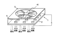
- FIG. 6 shows the general
- the lighting panel device 1 includes a fan 41 facing the organic EL panel 2 on the back wall side of the housing 5 that defines an internal space by a partition including the organic EL panel 2. Similar to the above-described embodiment, the organic EL panel 2 is provided with a plurality of through holes 4 formed on the surface thereof and penetrating from the internal space to the outside.
- the function of the through hole 4 can be fully utilized.
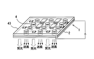
- FIG. 7 shows the general
- the control circuit board 43 of the organic EL panel 2 is provided on the surface opposite to the light emitting surface of the organic EL panel 2.
- An example of the control circuit board 43 is a control circuit board that drives the organic EL panel 2 in pulses for dimming the organic EL panel.
- the housing (not shown) for defining the internal space, the housing 5 communicating with the conduit from the blower shown in FIG. 1 or the housing of the lighting panel with a fan shown in FIG. The air is blown through the through hole 4 of the organic EL panel 2.
- FIG. 8 shows the top view of the illuminating device of the illumination panel with an air purifying mechanism of other embodiment by this invention.
- FIG. 9 is a sectional view taken along line AA in FIG.
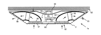
- the lighting device 1 a of the lighting panel with an air cleaning mechanism has a power receiving hook metal claw 51 (hook ceiling) provided at a substantially central portion on the back side of the housing 5, so that the ceiling of the house It is detachably fixed to a hooking rosette 63 attached to 62.
- an electrical connection portion CS for attaching and fixing the organic EL panel 2 is provided at a substantially central portion inside the housing 5, and a group of a plurality of through holes 52 serving as four suction ports is provided on the front surface of the organic EL panel 2. Similarly, four air outlets and a group of a plurality of through holes 53 are provided on the tapered side surface.
- the suction through holes 52 communicate with the blowing through holes 53 by the ducts 54 defined in the housing 5, and a dust collecting device 55 is provided in the middle of the duct 54.
- a blower 56 such as a multiblade fan is provided on the through hole 52 side.
- a control unit (not shown) is provided that is supplied with power from the hooking metal claw 51 and controls on / off of the dust collector 55 and the blower 56.
- a suction air filter 57 is provided along the organic EL panel 2 on the side of the air blower 56 of the duct 54 so as to be close to and opposed to the suction through hole 52, and close to and opposed to the blowout through hole 53.
- a blown air filter 58 is provided along the EL panel 2.
- the indoor air is sucked into the duct 54 from the suction through hole 52, and the oil component in the air is absorbed and removed by the suction air filter 57, and then collected.
- Smoke contained in the air is made smokeless or deodorized and purified by the dust device 55, and then passed through the blown air filter 58 to be further deodorized and then discharged again through the blowout through hole 53.
- the air in the vicinity of the ceiling can be efficiently purified by sucking indoor air from the front surface of the housing 5 and discharging it toward the side surface.
- a driving unit DS that is integrated with the organic EL panel 2 and controls the on / off and state of the organic EL panel 2 is provided.
- the suction air filter 57 and the blowout air filter 58 are fixed by fixing the electric connection half CS2 (hook metal claw part) connected to the drive part DS of the organic EL panel 2 to the electric connection part CS and receiving power. Can be protected.
- the housing 5 and the organic EL panel 2 are configured in a truncated pyramid shape with a square bottom in plan view, but the planar shape is not limited to this, and the planar shape is a polygon such as a triangle or a quadrangle, A circular or elliptical truncated cone shape may be used. That is, the organic EL panel 2 has at least two planes having different normal directions, and the through holes 4 need only be provided on both planes. Further, as shown in the schematic partial plan view of the organic EL panel 2 of the lighting panel with blower holes according to another embodiment shown in FIG. 10, the distances v between adjacent ones of the plurality of through holes 4 are equal.
- the luminance distribution of the organic EL panel 2 can be made uniform and the strength can be maintained.
- the shape of the through hole is not limited to a circle, and can be formed and used in an ellipse, a rectangle, or a polygon.
- the lighting device using the organic EL panel as the electroluminescence panel is exemplified.
- the organic EL panel 2 in the lighting device 1, 1a of the embodiment shown in FIG. 1, FIG. 6, FIG. 7 or FIG. instead of the above, an inorganic EL panel can be used.
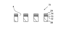
- An example of the inorganic EL panel 71 according to the present embodiment is shown in FIG. Examples of the inorganic EL panel 71 include those obtained by sequentially laminating a transmissive first electrode 72, a dielectric layer 73, and a light reflective second electrode 74 on the transparent substrate 20 such as glass.
- each inorganic EL element of an inorganic EL panel is an element provided with a plurality of inorganic material layers including a light emitting layer between a pair of opposed first and second electrodes carried on a substrate.
- the outer surface other than the blow-through hole 4 emits light and is used as illumination.
- the protective layer 24 is provided on the second electrode 74 side to form a laminated structure, and the inorganic EL panel 71 is configured.
- a compact illumination device can be provided, and since an electroluminescence panel that does not emit ultraviolet light is used, a yellow filter is not necessary.
- a plurality of through holes are provided directly in the electroluminescence lighting panel, and the through holes are used for blowing.
- the structure of the lighting device is simplified. Since the illumination and the ventilation can be performed by the same device, the space utilization efficiency is increased. By blowing air to the through-hole, the temperature of the electroluminescence panel is lowered and the light emission life is extended.
- ADVANTAGE OF THE INVENTION According to this invention, the illuminating device which can be integrated with an air conditioner, an air cleaner other than clean room illumination can be obtained.
Landscapes
- Engineering & Computer Science (AREA)
- General Engineering & Computer Science (AREA)
- Chemical & Material Sciences (AREA)
- Combustion & Propulsion (AREA)
- Mechanical Engineering (AREA)
- Physics & Mathematics (AREA)
- Optics & Photonics (AREA)
- Electroluminescent Light Sources (AREA)
- Arrangement Of Elements, Cooling, Sealing, Or The Like Of Lighting Devices (AREA)
- Non-Portable Lighting Devices Or Systems Thereof (AREA)
Abstract
Description
図1にエレクトロルミネッセンスパネルとして有機ELパネルを用いた本実施形態の送風孔付照明パネル装置1を示す。照明パネルの本体としては面発光体である板状の有機ELパネル2が用いられる。有機ELパネル2には、その表面に形成され内部空間から外部へ貫通する複数の貫通孔4が設けられている。送風孔付照明パネル装置1は、有機ELパネル2を含む隔壁によって内部空間を画定するハウジング5を備えている。送風装置(図示せず)からの空気3が導管6を介してハウジング5へ供給され、この貫通孔4から送風が行われる。有機ELパネル2の貫通孔4以外の外面は発光して照明として用いられる。図1に示すように、貫通孔4に平行に対向してハウジング5の内部空間に、HEPA(high efficiency particulate air)フィルタやULPA(ultra low penetration air)フィルタなどの塵埃エアフィルタFを設けることができる。
以下に、本実施形態による有機ELパネル2の一例を詳述する。図5に示すように、ガラスなどの透明基板20上にて、順に、透明な陽極21(第1電極)、正孔注入層33、正孔輸送層34、発光層35、正孔阻止層36、電子輸送層37、電子注入層38及び金属からなる陰極(第2電極)22が積層されて得られるものが挙げられる。正孔注入層33、正孔輸送層34、発光層35、正孔阻止層36、及び電子輸送層37は有機材料層23である。すなわち、有機EL素子において、対向する1対の陽極及び陰極の間に積層配置された複数の有機材料層が正孔注入層、正孔輸送層、発光層、正孔阻止層、電子輸送層、電子注入層を包含する。これら有機材料層などの構成要素については後述する。このように有機ELパネルの各有機EL素子は、対向する1対の陽極及び陰極の間に積層配置されかつ発光層を含む複数の有機材料層を備えた有機EL素子である。なお、発光層、正孔注入層、正孔輸送層などのいずれの有機材料層は、真空蒸着法など乾式成膜方法やインクジェット法など湿式塗布方法にて成膜され得る。
基板20としては、石英やガラスの板、金属板や金属箔、曲げられる樹脂基板、プラスチックフィルムやシートなどが用いられる。特にガラス板や、ポリエステル、ポリメタクリレート、ポリカーボネート、ポリスルホンなどの透明な合成樹脂の板が好ましい。合成樹脂基板を使用する場合にはガスバリア性に留意する必要がある。基板のガスバリア性が小さすぎると、基板を通過した外気により有機EL素子が劣化することがあるので好ましくない。このため、合成樹脂基板の少なくとも片面に緻密なシリコン酸化膜などを設けてガスバリア性を確保する方法も好ましい方法の一つである。
発光層までの層に正孔を供給する陽極21は、通常、アルミニウム、金、銀、ニッケル、パラジウム、白金などの金属、インジウム及び/又はスズ、亜鉛の酸化物(ITOやIZO)などの金属酸化物、ヨウ化銅などのハロゲン化金属、カーボンブラック、或いは、ポリ(3-メチルチオフェン)、ポリピロール、ポリアニリンなどの導電性高分子などにより構成される。
正孔注入層33、正孔輸送層34、発光層35、電子輸送層36及び電子注入層37の主成分を構成する有機材料層は、電荷輸送性(正孔及び/又は電子の移動性)を有する有機化合物を利用する。
図6は本発明による他の実施形態のファン付照明パネルの照明装置の概略部分切欠斜視図を示す。この照明パネル装置1は、有機ELパネル2を含む隔壁によって内部空間を画定するハウジング5の奥壁側に、有機ELパネル2に対向してファン41を備えている。有機ELパネル2には、上記の実施形態と同様に、その表面に形成され内部空間から外部へ貫通する複数の貫通孔4が設けられている。
図7は本発明による他の実施形態の貫通孔付照明パネルの照明装置の概略部分切欠斜視図を示す。この照明パネル装置1は、有機ELパネル2の発光面の反対側の面に有機ELパネル2の制御回路基板43を設けてある。制御回路基板43としては有機ELパネル調光のために有機ELパネル2をパルス駆動する制御回路基板が挙げられる。内部空間を画定するハウジング(図示せず)としては、上記の実施形態と同様に、図1に示す送風装置からの導管に連通したハウジング5としたり、図6に示すファン付の照明パネルのハウジング5とすることができ、有機ELパネル2の貫通孔4を通して送風が行われる。
図8は本発明による他の実施形態の空気清浄機構付照明パネルの照明装置の平面図を示す。図9は図8中のA-A線の断面図を示す。
上記照明装置においては、エレクトロルミネッセンスパネルとして有機ELパネルを用いた照明装置を例示したが、図1、図6、図7又は図8に示した実施形態の照明装置1、1aにおける有機ELパネル2に代えて無機ELパネルを用いることもできる。本実施形態による無機ELパネル71の一例を図11に示す。無機ELパネル71は、ガラスなどの透明基板20上にて、順に、透過性の第1電極72、誘電体層73、光反射性の第2電極74が積層されて得られるものが挙げられる。誘電体層73には、発光層と絶縁層の交互の積層構造が採用できる。発光層には、SrGa2S4:Eu(緑)、CaS:Eu(赤)、BaAl2S4:Eu(青)などの硫化物、酸化物が用いられ、絶縁層には、チタン酸ストロンチウム(SrTiO3)などの酸化物が用いられる。このように無機ELパネルの各無機EL素子は、基板に担持された、対向する1対の第1及び第2電極の間に発光層を含む複数の無機材料層を備えた素子である。送風用の貫通孔4以外の外面は発光して照明として用いられる。第2電極74側には保護層24が設けられ積層構造となって無機ELパネル71が構成されている。
2 有機ELパネル
4 貫通孔
5 ハウジング
6 導管
20 基板
21 陽極(第1電極)
22 陰極(第2電極)
51 引掛金属爪部
52 吸込貫通孔
53 吹出貫通孔
54 ダクト
55 集塵装置
56 送風装置
57 吸入エアフィルタ
58 吹出エアフィルタ
62 天井
63 引掛ローゼット
71 無機ELパネル
CS2 電気接続半体
CS 電気接続部
Claims (5)
- 面発光体と前記面発光体を含む隔壁によって内部空間を画定するハウジングとを備えた照明装置であって、
前記面発光体は、透過性の基板を有して可視光を面状に放射するエレクトロルミネッセンスパネルであり、
前記エレクトロルミネッセンスパネルは前記内部空間から外部へ貫通する複数の貫通孔を有することを特徴とする照明装置。 - 前記エレクトロルミネッセンスパネルは有機エレクトロルミネッセンスパネルであることを特徴とする請求項1に記載の照明装置。
- 前記エレクトロルミネッセンスパネルは無機エレクトロルミネッセンスパネルであることを特徴とする請求項1に記載の照明装置。
- 前記貫通孔に対向して前記内部空間に設けられたエアフィルタを有することを特徴とする請求項1乃至3のいずれか1項に記載の照明装置。
- 前記エレクトロルミネッセンスパネルが法線の方向が異なる少なくとも2つの平面を有し、前記貫通孔が前記2つの平面の双方に設けられており、前記2つの平面の一方と他方との前記貫通孔を連通せしめるダクトを有することを特徴とする請求項4に記載の照明装置。
Priority Applications (3)
| Application Number | Priority Date | Filing Date | Title |
|---|---|---|---|
| US14/116,119 US20140185305A1 (en) | 2011-05-11 | 2011-05-11 | Lighting device |
| PCT/JP2011/060874 WO2012153407A1 (ja) | 2011-05-11 | 2011-05-11 | 照明装置 |
| JP2012510833A JP5022525B1 (ja) | 2011-05-11 | 2011-05-11 | 照明装置 |
Applications Claiming Priority (1)
| Application Number | Priority Date | Filing Date | Title |
|---|---|---|---|
| PCT/JP2011/060874 WO2012153407A1 (ja) | 2011-05-11 | 2011-05-11 | 照明装置 |
Publications (1)
| Publication Number | Publication Date |
|---|---|
| WO2012153407A1 true WO2012153407A1 (ja) | 2012-11-15 |
Family
ID=46980531
Family Applications (1)
| Application Number | Title | Priority Date | Filing Date |
|---|---|---|---|
| PCT/JP2011/060874 Ceased WO2012153407A1 (ja) | 2011-05-11 | 2011-05-11 | 照明装置 |
Country Status (3)
| Country | Link |
|---|---|
| US (1) | US20140185305A1 (ja) |
| JP (1) | JP5022525B1 (ja) |
| WO (1) | WO2012153407A1 (ja) |
Cited By (3)
| Publication number | Priority date | Publication date | Assignee | Title |
|---|---|---|---|---|
| JP2014126313A (ja) * | 2012-12-27 | 2014-07-07 | Ntt Facilities Inc | ダクト空調システム |
| WO2015001040A1 (de) * | 2013-07-05 | 2015-01-08 | Osram Oled Gmbh | Organische leuchtdiode und verfahren zum betreiben einer organischen leuchtdiode |
| EP3004722A4 (en) * | 2013-05-30 | 2018-01-24 | Nortek Air Solutions, LLC | Illuminating airflow panel assembly |
Families Citing this family (14)
| Publication number | Priority date | Publication date | Assignee | Title |
|---|---|---|---|---|
| US20170200569A1 (en) * | 2014-07-16 | 2017-07-13 | Showa Denko K.K. | Method for producing solid electrolytic capacitor element |
| US20160166136A1 (en) * | 2014-12-10 | 2016-06-16 | Boston Scientific Scimed, Inc. | Thermal management for medical devices and related methods of use |
| US10775037B2 (en) | 2015-07-01 | 2020-09-15 | Sld Technology, Inc. | Airflow-channeling surgical light system and method |
| US9895202B2 (en) * | 2015-07-01 | 2018-02-20 | Sld Technology, Inc. | Airflow-channeling surgical light system and method |
| DE102015225815B4 (de) * | 2015-12-17 | 2022-05-25 | Viessmann Werke Gmbh & Co Kg | Vorrichtung und System zum Heizen, Kühlen, Belüften und Beleuchten eines Innenraums |
| KR102531643B1 (ko) | 2016-01-15 | 2023-05-11 | 삼성전자주식회사 | 공기조화기 |
| CN108779912A (zh) * | 2016-02-22 | 2018-11-09 | 飞利浦照明控股有限公司 | 具有集成空气倍增器的照明器 |
| WO2017195041A1 (en) * | 2016-05-12 | 2017-11-16 | Price Industries Limited | Laminar flow diffuser with integrated lighting |
| US11054169B2 (en) * | 2016-05-12 | 2021-07-06 | Price Industries Limited | Laminar flow diffuser with integrated lighting |
| US11389361B2 (en) * | 2016-11-08 | 2022-07-19 | Optimus Licensing Ag | Integrated operating room lighting and patient warming system—design and components |
| TWI741539B (zh) * | 2019-05-02 | 2021-10-01 | 國立成功大學 | 手術煙霧移除裝置及方法 |
| PL4053466T3 (pl) * | 2021-03-01 | 2025-12-08 | Halton Oy | Urządzenie końcowe z integralną oprawą oświetleniową |
| TWI852005B (zh) * | 2021-10-21 | 2024-08-11 | 群創光電股份有限公司 | 電子裝置 |
| IT202200024621A1 (it) * | 2022-11-29 | 2024-05-29 | Ecoprogetti S R L | Apparato simulatore solare |
Citations (4)
| Publication number | Priority date | Publication date | Assignee | Title |
|---|---|---|---|---|
| WO2005123246A1 (ja) * | 2004-06-15 | 2005-12-29 | Sumitomo Electric Industries, Ltd. | 面発光デバイス、及びこれを用いたろ過フィルタ、光アシスト型セラミックフィルタ |
| JP2007109552A (ja) * | 2005-10-14 | 2007-04-26 | Alps Electric Co Ltd | 板ばね付きシート、及び入力装置 |
| JP2007271250A (ja) * | 2006-03-07 | 2007-10-18 | Takafumi Wada | 輻射空調ユニット |
| JP2009158103A (ja) * | 2007-12-25 | 2009-07-16 | Panasonic Electric Works Co Ltd | El照明装置 |
Family Cites Families (2)
| Publication number | Priority date | Publication date | Assignee | Title |
|---|---|---|---|---|
| US20040081596A1 (en) * | 2002-10-23 | 2004-04-29 | Hsi Cheng Huang | Device case and air purifier arrangement |
| US20070081320A1 (en) * | 2005-08-08 | 2007-04-12 | Mark Gilbert | Electroluminescent illumination for audio components |
-
2011
- 2011-05-11 US US14/116,119 patent/US20140185305A1/en not_active Abandoned
- 2011-05-11 WO PCT/JP2011/060874 patent/WO2012153407A1/ja not_active Ceased
- 2011-05-11 JP JP2012510833A patent/JP5022525B1/ja not_active Expired - Fee Related
Patent Citations (4)
| Publication number | Priority date | Publication date | Assignee | Title |
|---|---|---|---|---|
| WO2005123246A1 (ja) * | 2004-06-15 | 2005-12-29 | Sumitomo Electric Industries, Ltd. | 面発光デバイス、及びこれを用いたろ過フィルタ、光アシスト型セラミックフィルタ |
| JP2007109552A (ja) * | 2005-10-14 | 2007-04-26 | Alps Electric Co Ltd | 板ばね付きシート、及び入力装置 |
| JP2007271250A (ja) * | 2006-03-07 | 2007-10-18 | Takafumi Wada | 輻射空調ユニット |
| JP2009158103A (ja) * | 2007-12-25 | 2009-07-16 | Panasonic Electric Works Co Ltd | El照明装置 |
Cited By (3)
| Publication number | Priority date | Publication date | Assignee | Title |
|---|---|---|---|---|
| JP2014126313A (ja) * | 2012-12-27 | 2014-07-07 | Ntt Facilities Inc | ダクト空調システム |
| EP3004722A4 (en) * | 2013-05-30 | 2018-01-24 | Nortek Air Solutions, LLC | Illuminating airflow panel assembly |
| WO2015001040A1 (de) * | 2013-07-05 | 2015-01-08 | Osram Oled Gmbh | Organische leuchtdiode und verfahren zum betreiben einer organischen leuchtdiode |
Also Published As
| Publication number | Publication date |
|---|---|
| JPWO2012153407A1 (ja) | 2014-07-28 |
| JP5022525B1 (ja) | 2012-09-12 |
| US20140185305A1 (en) | 2014-07-03 |
Similar Documents
| Publication | Publication Date | Title |
|---|---|---|
| JP5022525B1 (ja) | 照明装置 | |
| KR101784804B1 (ko) | 유기발광소자 | |
| US8502208B2 (en) | Organic light-emitting device | |
| KR101135541B1 (ko) | 유기 발광 장치 | |
| EP1978574A2 (en) | Organic electroluminescent device | |
| CN103053221B (zh) | 有机电致发光器件 | |
| JP2004349138A (ja) | 有機電界発光素子及びその製造方法 | |
| CN1905238A (zh) | 白色有机发光二极管及其制备方法 | |
| JP2007502534A (ja) | 有機ダイオードの交流駆動用回路配置 | |
| KR101589343B1 (ko) | 유기전자소자용 기판 | |
| CN1778147A (zh) | 有机电致发光元件以及显示装置 | |
| JP3599077B2 (ja) | 有機エレクトロルミネッセンス素子とその製造方法 | |
| JP6151874B1 (ja) | 有機エレクトロルミネッセント装置および照明装置 | |
| CN108123050A (zh) | 一种以交流驱动的白光oled器件 | |
| KR20160084282A (ko) | 탠덤형 유기발광소자 | |
| TWI224943B (en) | Organic electroluminescence device and fabricating method thereof | |
| JP2012238575A (ja) | 照明装置 | |
| JP6282328B2 (ja) | 発光装置 | |
| JP6133301B2 (ja) | 発光装置 | |
| US20160323965A1 (en) | Light-emitting device | |
| JP2007053091A (ja) | 白色有機発光素子及びその製造方法 | |
| WO2012169069A1 (ja) | 有機エレクトロルミネッセンスパネル | |
| JPH07176384A (ja) | 有機el素子 | |
| CN114122098B (zh) | 一种有机电致发光装置、显示装置和照明装置 | |
| KR20130135142A (ko) | 유기전자장치 |
Legal Events
| Date | Code | Title | Description |
|---|---|---|---|
| ENP | Entry into the national phase |
Ref document number: 2012510833 Country of ref document: JP Kind code of ref document: A |
|
| 121 | Ep: the epo has been informed by wipo that ep was designated in this application |
Ref document number: 11864925 Country of ref document: EP Kind code of ref document: A1 |
|
| NENP | Non-entry into the national phase |
Ref country code: DE |
|
| WWE | Wipo information: entry into national phase |
Ref document number: 14116119 Country of ref document: US |
|
| 122 | Ep: pct application non-entry in european phase |
Ref document number: 11864925 Country of ref document: EP Kind code of ref document: A1 |