WO2012147544A1 - Cooler for semiconductor module, and semiconductor module - Google Patents
Cooler for semiconductor module, and semiconductor module Download PDFInfo
- Publication number
- WO2012147544A1 WO2012147544A1 PCT/JP2012/060215 JP2012060215W WO2012147544A1 WO 2012147544 A1 WO2012147544 A1 WO 2012147544A1 JP 2012060215 W JP2012060215 W JP 2012060215W WO 2012147544 A1 WO2012147544 A1 WO 2012147544A1
- Authority
- WO
- WIPO (PCT)
- Prior art keywords
- flow path
- refrigerant
- water jacket
- semiconductor module
- cooler
- Prior art date
Links
Images


Classifications
-
- H—ELECTRICITY
- H05—ELECTRIC TECHNIQUES NOT OTHERWISE PROVIDED FOR
- H05K—PRINTED CIRCUITS; CASINGS OR CONSTRUCTIONAL DETAILS OF ELECTRIC APPARATUS; MANUFACTURE OF ASSEMBLAGES OF ELECTRICAL COMPONENTS
- H05K7/00—Constructional details common to different types of electric apparatus
- H05K7/20—Modifications to facilitate cooling, ventilating, or heating
- H05K7/20218—Modifications to facilitate cooling, ventilating, or heating using a liquid coolant without phase change in electronic enclosures
- H05K7/20254—Cold plates transferring heat from heat source to coolant
-
- H—ELECTRICITY
- H01—ELECTRIC ELEMENTS
- H01L—SEMICONDUCTOR DEVICES NOT COVERED BY CLASS H10
- H01L23/00—Details of semiconductor or other solid state devices
- H01L23/34—Arrangements for cooling, heating, ventilating or temperature compensation ; Temperature sensing arrangements
- H01L23/36—Selection of materials, or shaping, to facilitate cooling or heating, e.g. heatsinks
- H01L23/373—Cooling facilitated by selection of materials for the device or materials for thermal expansion adaptation, e.g. carbon
- H01L23/3735—Laminates or multilayers, e.g. direct bond copper ceramic substrates
-
- H—ELECTRICITY
- H01—ELECTRIC ELEMENTS
- H01L—SEMICONDUCTOR DEVICES NOT COVERED BY CLASS H10
- H01L23/00—Details of semiconductor or other solid state devices
- H01L23/34—Arrangements for cooling, heating, ventilating or temperature compensation ; Temperature sensing arrangements
- H01L23/46—Arrangements for cooling, heating, ventilating or temperature compensation ; Temperature sensing arrangements involving the transfer of heat by flowing fluids
- H01L23/473—Arrangements for cooling, heating, ventilating or temperature compensation ; Temperature sensing arrangements involving the transfer of heat by flowing fluids by flowing liquids
-
- H—ELECTRICITY
- H05—ELECTRIC TECHNIQUES NOT OTHERWISE PROVIDED FOR
- H05K—PRINTED CIRCUITS; CASINGS OR CONSTRUCTIONAL DETAILS OF ELECTRIC APPARATUS; MANUFACTURE OF ASSEMBLAGES OF ELECTRICAL COMPONENTS
- H05K7/00—Constructional details common to different types of electric apparatus
- H05K7/20—Modifications to facilitate cooling, ventilating, or heating
- H05K7/2089—Modifications to facilitate cooling, ventilating, or heating for power electronics, e.g. for inverters for controlling motor
- H05K7/20927—Liquid coolant without phase change
-
- H—ELECTRICITY
- H01—ELECTRIC ELEMENTS
- H01L—SEMICONDUCTOR DEVICES NOT COVERED BY CLASS H10
- H01L2224/00—Indexing scheme for arrangements for connecting or disconnecting semiconductor or solid-state bodies and methods related thereto as covered by H01L24/00
- H01L2224/01—Means for bonding being attached to, or being formed on, the surface to be connected, e.g. chip-to-package, die-attach, "first-level" interconnects; Manufacturing methods related thereto
- H01L2224/26—Layer connectors, e.g. plate connectors, solder or adhesive layers; Manufacturing methods related thereto
- H01L2224/31—Structure, shape, material or disposition of the layer connectors after the connecting process
- H01L2224/32—Structure, shape, material or disposition of the layer connectors after the connecting process of an individual layer connector
- H01L2224/321—Disposition
- H01L2224/32151—Disposition the layer connector connecting between a semiconductor or solid-state body and an item not being a semiconductor or solid-state body, e.g. chip-to-substrate, chip-to-passive
- H01L2224/32221—Disposition the layer connector connecting between a semiconductor or solid-state body and an item not being a semiconductor or solid-state body, e.g. chip-to-substrate, chip-to-passive the body and the item being stacked
- H01L2224/32225—Disposition the layer connector connecting between a semiconductor or solid-state body and an item not being a semiconductor or solid-state body, e.g. chip-to-substrate, chip-to-passive the body and the item being stacked the item being non-metallic, e.g. insulating substrate with or without metallisation
-
- H—ELECTRICITY
- H01—ELECTRIC ELEMENTS
- H01L—SEMICONDUCTOR DEVICES NOT COVERED BY CLASS H10
- H01L2924/00—Indexing scheme for arrangements or methods for connecting or disconnecting semiconductor or solid-state bodies as covered by H01L24/00
- H01L2924/10—Details of semiconductor or other solid state devices to be connected
- H01L2924/11—Device type
- H01L2924/13—Discrete devices, e.g. 3 terminal devices
- H01L2924/1304—Transistor
- H01L2924/1305—Bipolar Junction Transistor [BJT]
- H01L2924/13055—Insulated gate bipolar transistor [IGBT]
Definitions
- the present invention relates to a semiconductor module cooler for supplying a coolant to a water jacket from the outside and cooling a semiconductor element disposed on the outer surface of the water jacket, and a semiconductor module including the cooler.
- Semiconductor modules are widely used in power converters represented by hybrid vehicles and electric vehicles.
- a semiconductor module constituting a control device for energy saving a power semiconductor element is provided to control a large current.
- Such power semiconductor elements tend to increase the amount of heat generated when controlling a large current.
- the cooling method of the semiconductor module including a plurality of power semiconductor elements becomes a serious problem.
- a liquid cooling type cooler (hereinafter also referred to as “cooling device”) has been conventionally used for the semiconductor module.
- a liquid cooling type cooling device that circulates a refrigerant
- the flow rate of the refrigerant is increased
- the heat radiation fin has a good heat transfer coefficient, or the fin is configured.
- Various ideas have been made, such as increasing the thermal conductivity of materials.
- a refrigerant introduction flow path for introducing the refrigerant and a refrigerant discharge flow path for discharging the refrigerant are arranged in parallel with each other.
- a plurality of heat sinks are arranged in the refrigerant flow direction substantially orthogonal to each other (see Patent Documents 1 to 7).
- the cooling performance per pressure loss can be increased.
- the pressure loss of the refrigerant in the flow path as a whole can be reduced, and the cooling efficiency can be improved (patent) Reference 5).
- Patent Document 6 the entire rear side wall of the casing is smoothly inclined forward from the right side wall toward the left side wall, and the flow path cross-sectional area of the inlet header portion is from the coolant inlet side.
- a liquid-cooling type cooling device that decreases toward the left side wall is described (see paragraph numbers [0024] and [0031] and FIG. 2).
- Patent Document 3 describes a liquid cooling type cooling device in which flow paths through which refrigerant is introduced and discharged are arranged on the same side surface of the module, and each flow path is arranged in a direction orthogonal to the fin without change in cross-sectional area. (See FIG. 1).
- the distribution of the unbalanced refrigerant flows due to the shape of the heat sink and the refrigerant flow path, the arrangement method of the heating elements, the shape of the refrigerant inlet and outlet, and the like.
- such a drift distribution causes a bias in the cooling performance. Therefore, it is difficult to obtain a stable cooling performance with little unevenness in the entire cooling device.
- the present invention has been made in view of the above-described points, eliminates the drift generated in the flow path of the refrigerant, effectively cools the semiconductor element disposed on the outer surface, and malfunctions or breaks due to heat generation of the semiconductor element.
- An object of the present invention is to provide a semiconductor module cooler capable of reliably preventing the above.
- Another object of the present invention is to provide a semiconductor module in which semiconductor elements are arranged on the outer surface of such a cooler.
- the present invention provides a semiconductor module cooler that supplies a coolant to the water jacket from the outside and cools the semiconductor elements disposed on the outer surface thereof.
- the semiconductor module cooler includes a heat sink thermally connected to the semiconductor element, and extends from the coolant introduction port into the water jacket and guides the coolant toward one side surface of the heat sink.
- the introduction port and the coolant discharge port are formed on the same wall surface of the water jacket, and the heat sink is disposed in the third flow path.
- the semiconductor module of the present invention includes a cooler that supplies a coolant to the water jacket from the outside and cools the semiconductor element disposed on the outer surface thereof, and is thermally connected to the semiconductor element. And a first flow path in which a guide portion having an inclined surface for guiding the refrigerant toward the one side surface of the heat sink is disposed in the water jacket. A second flow path disposed in the water jacket in parallel with the first flow path, extending to the coolant discharge port, and having a side wall parallel to the other side surface of the heat sink; and the water jacket A third flow passage formed at a position where the first flow passage and the second flow passage communicate with each other, wherein the refrigerant inlet and the refrigerant outlet are the water jacket. Is the formed on the same wall, the heat sink is characterized in that it is disposed in the third flow path.
- the semiconductor module cooler of the present invention by setting the cross-sectional area of the introduction path to be smaller than that of the discharge path so that the refrigerant flows toward one side of the heat sink, the flow velocity in the vicinity of the refrigerant inlet is reduced. As a result, the temperature rise can be eliminated, and the flow rate of the refrigerant flowing into the heat sink from the first flow path can be adjusted.
- the separation wall that divides the refrigerant flow path in the first flow path is provided to suppress an increase in pressure loss caused by narrowing the cross-sectional area of the introduction path.
- the flow rate distribution of the refrigerant can be adjusted. Accordingly, the semiconductor element disposed on the outer surface of the cooler can be effectively cooled, and the semiconductor element can be stably operated.
- FIG. 2 is a schematic diagram illustrating an example of the semiconductor module in FIG. It is a perspective view which shows the principal part structure of the water jacket of a cooler. It is a figure explaining the shape of two kinds of fins, Comprising: (A) is a perspective view which shows a blade fin, (B) is a perspective view which shows a corrugated fin. It is a figure which shows an example of the power converter circuit comprised as a semiconductor module.
- (A) is a perspective view which shows the example of arrangement
- (B) is a perspective view which showed the principal part structure of the water jacket of a cooler. is there. It is a perspective view which shows the shape of the water jacket of the type different from the cooler of FIG. 6 (B). It is a figure which shows the flow rate of the refrigerant
- FIG. 16A is a diagram showing a refrigerant flow velocity distribution for each position of the circuit board
- FIG. 17B is a diagram showing a pressure difference between the refrigerant inlet and outlet.
- FIG. 20 is a partial plan view showing an introduction path shape of a water jacket of type N different from the cooler of FIG. 19. 15, 19, and 20, (A) shows a refrigerant flow velocity distribution for each position of the circuit board, and (B) shows a pressure difference between the refrigerant inlet and outlet.
- FIG. It is a figure which shows the performance of the water jacket of FIG.15, FIG.19 and FIG.20 according to the type.
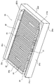
- FIG. 1 is a perspective view showing the appearance of a semiconductor module of the present invention
- FIG. 2 is a schematic view showing an example of the semiconductor module of FIG.
- FIG. 3 is a perspective view showing the configuration of the main part of the water jacket of the cooler, and the arrows indicate the direction in which the refrigerant flows.
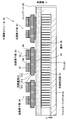
- the semiconductor module 10 includes a cooler 2 and a plurality of circuit element portions 3A to 3C arranged on the cooler 2, as shown in FIGS.
- the cooler 2 includes a water jacket 2A as a fin cover and a fin base 2B in which a plurality of fins 2C as heat sinks are planted, and the plurality of fins 2C are accommodated in the water jacket 2A. ing.
- the direction to which the fin base 2B is attached in FIG. 2 is “upper”, and the upper direction of the water jacket 2A is upward in FIG.
- the “front side” and the side where the introduction port 24 and the discharge port 25 are formed are referred to as “left side” and the like.
- the flow of the refrigerant in the cooler 2 is defined as “upstream side”.
- the outer shape of the water jacket 2A of the cooler 2 is a substantially rectangular parallelepiped shape.
- the upper main surface is provided with a coolant introduction channel 21, an introduction port 21a, a refrigerant discharge channel 22, a discharge port 22a, and a cooling channel 23 for disposing the fins 2C.
- the water jacket 2A is provided with an inlet 24 for introducing the refrigerant into the left side wall 2Ab and an outlet 25 for discharging the refrigerant to the outside on the left side wall 2Ab on the same side. Yes.
- These refrigerant introduction channels 21 and the like are defined by the front side wall 2Aa, the left side wall 2Ab, the rear side wall 2Ac, the right side wall 2Ad, and the bottom wall 2Ae.
- the fin 2C is drawn on the figure for convenience of explanation.
- the refrigerant introduction channel 21 extends as a first channel from the introduction port 24 to the right side wall 2Ad in parallel with the front side wall 2Aa of the water jacket 2A through the introduction port 21a so as to follow the inflow direction of the refrigerant. Be present.
- coolant discharge flow path 22 is a straight line from the right side wall 2Ad to the discharge port 25 via the discharge port part 22a in parallel with the rear side wall 2Ac so that it may go to the refrigerant
- the refrigerant introduction channel 21 and the refrigerant discharge channel 22 are provided substantially in parallel.
- a guide portion 21Si having an inclination of 60 ° or less is provided at the end portion of the refrigerant flowing into the refrigerant introduction passage 21 from the introduction port 24 and the start end portion of the refrigerant discharge passage 22 through which the refrigerant flows out to the discharge port 25. , 22So.
- the cooling flow path 23 is disposed as a third flow path between the refrigerant introduction flow path 21 and the refrigerant discharge flow path 22 and is formed so as to communicate with the refrigerant introduction flow path 21 and the refrigerant discharge flow path 22. ing.
- the cooling flow path 23 extends in a direction orthogonal to the extending direction of the refrigerant introduction flow path 21 and the extending direction of the refrigerant discharge flow path 22.
- the inner surfaces of the left side wall 2Ab and the right side wall 2Ad that define the boundary of the cooling channel 23 are formed perpendicular to the bottom surface of the cooling channel 23 and the inner surface of the rear side wall 2Ac, respectively.
- a heat sink composed of a plurality of fins 2C is arranged, and the refrigerant flows through the channel defined by the fins 2C. Then, the refrigerant introduced from the introduction port 24 is discharged from the discharge port 25 through the refrigerant introduction channel 21, the cooling channel 23, and the refrigerant discharge channel 22 in the water jacket 2 ⁇ / b> A.
- the heat sink has a substantially rectangular parallelepiped shape, and is disposed in the cooling flow path 23 so that the left side surface, the rear side surface, and the right side surface thereof are parallel to the inner surfaces of the left side wall 2Ab, the rear side wall 2Ac, and the right side wall 2Ad. ing.
- the plurality of fins 2C are arranged so as to be parallel to the inner surface of the left side wall 2Ab or the right side wall 2Ad, respectively.
- the water jacket 2A having such a configuration can be formed using a metal material such as aluminum, aluminum alloy, copper, or copper alloy.
- a metal material such as aluminum, aluminum alloy, copper, or copper alloy.
- the water jacket 2A is formed using such a metal material, for example, the above-described refrigerant introduction flow path 21, refrigerant discharge flow path 22, cooling flow path 23, introduction port 24, and discharge port are formed by die casting. 25 can be formed.
- the water jacket 2A can use a material containing a carbon filler.
- a ceramic material, a resin material, or the like can be used depending on the type of the refrigerant, the temperature of the refrigerant flowing in the water jacket 2A, and the like.
- the refrigerant introduction passage 24, the refrigerant discharge passage 22, and the formation surface side of the plurality of cooling passages 23 are arranged so that the refrigerant inlet 24 as shown in FIGS. 1 and 2.
- the fin base 2B is sealed except for the discharge port 25.
- a plurality of fins 2C are implanted in the base material 26.
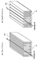
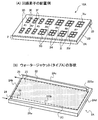
- FIG. 4A and 4B are diagrams for explaining the shapes of two types of fins.
- FIG. 4A is a perspective view showing a blade fin
- FIG. 4B is a perspective view showing a corrugated fin.
- the fins 2 ⁇ / b> C of the cooler 2 can be formed as a plurality of blade fins 2 ⁇ / b> Ca in which plate-like fins are juxtaposed as shown in FIG. 4 (A), for example.
- the blade fin 2Ca is disposed in the cooling flow path 23, and the refrigerant flows in the direction indicated by the arrow in FIG. At this time, the blade fins 2Ca are held by the base material 26 and the fin base 2B in the cooling channel 23.
- FIG. 4A illustrates the blade fin 2Ca
- the corrugated fin 2Cb shown in FIG. 4B can also be used.
- the fin 2C having the shape of the blade fin 2Ca or the corrugated fin 2Cb is integrated with the fin base 2B and disposed toward the water jacket 2A on the fin 2C side, as shown in FIG. 2, for example.
- the fin 2C is formed in a dimension (height) such that a certain clearance C exists between the tip of the fin 2C and the bottom wall 2Ae of the water jacket 2A.
- the base material 26 is integrated with the fin base 2B, and when the fin 2C side of the fin base 2B is arranged facing the water jacket 2A, the fin 2C is in the cooling channel 23 of the water jacket 2A. It is supposed to be arranged in. Note that the fin 2C is formed integrally with the fin base 2B itself, such as die-casting or brazing, or the fin 2C is formed in a convex shape from the fin base 2B by die casting, and then the fin shape is formed by the wire cutting method. Is possible.
- the fin shape of the fin 2C a variety of conventionally known shapes can be used. Since the fin 2C serves as a resistance of the refrigerant flowing in the cooling flow path 23, it is desirable that the fin 2C has a small pressure loss with respect to the refrigerant.
- the shape and dimensions of the fins 2C are appropriately set in consideration of the conditions for introducing the refrigerant into the cooler 2 (that is, pump performance, etc.), the type of refrigerant (viscosity, etc.), the target heat removal amount, and the like. Is preferred.
- the external shape of the heat sink composed of the fins 2C is a substantially rectangular parallelepiped, preferably a rectangular parallelepiped, and may be chamfered or deformed as long as the effects of the invention are not impaired.
- the fin 2C and the fin base 2B can be formed using a metal material such as aluminum, an aluminum alloy, copper, a copper alloy, etc., similarly to the water jacket 2A.
- the fins 2 ⁇ / b> C can be formed by joining, for example, predetermined pins or plates formed using a metal material to the metal base material 26 in addition to the blade fins 2 ⁇ / b> Ca and the corrugated fins 2 ⁇ / b> Cb described above.
- the base material 26 to which the fins 2C are bonded in this way is bonded to a predetermined region of the fin base 2B such as a metal plate, that is, a region corresponding to the cooling flow path 23 shown in FIG. In this way, not only the base material 26 to which the fins 2C are previously bonded can be bonded to the fin base 2B, but also a plurality of fins 2C can be directly bonded to the fin base 2B to constitute a heat sink.
- the inlet 24 is connected to a pump provided on the upstream side thereof, and the discharge port 25 is connected to a heat exchanger provided on the downstream side thereof.
- a closed-loop refrigerant flow path including the vessel is configured. The refrigerant is forcibly circulated in such a closed loop by a pump.
- each of the circuit element units 3A to 3C has a configuration in which a total of four two types of semiconductor elements 32 and 33 are mounted on the substrate 31, respectively.
- the substrate 31 has a configuration in which conductor patterns 31b and 31c are formed on both surfaces of an insulating substrate 31a.
- the insulating substrate 31a of the substrate 31 for example, a ceramic substrate such as aluminum nitride or aluminum oxide can be used.
- the conductor patterns 31b and 31c on the insulating substrate 31a can be formed using a metal such as copper or aluminum (for example, copper foil).
- the semiconductor elements 32 and 33 are bonded to the conductor pattern 31b side of the substrate 31 using a bonding layer 34 such as solder, and are electrically connected to the conductor pattern 31b directly or via a wire (not shown).
- the substrate 31 on which the semiconductor elements 32 and 33 are mounted is bonded to the fin base 2B of the cooler 2 via the bonding layer 35 on the other conductor pattern 31c side.
- the substrate 31 and the semiconductor elements 32 and 33 mounted on the substrate 31 are thermally connected to the cooler 2.
- the exposed surfaces of the conductor patterns 31b and 31c and the wire surfaces that electrically connect the semiconductor elements 32 and 33 and the conductor pattern 31b are protected from contamination, corrosion, external force, etc. by nickel plating or the like.
- a protective layer may be formed.
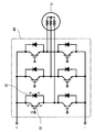
- FIG. 5 is a diagram illustrating an example of a power conversion circuit configured as a semiconductor module.
- power semiconductor elements are used as the semiconductor elements 32 and 33 mounted on the substrate 31.
- one semiconductor element 32 may be a free wheeling diode (FWD)
- the other semiconductor element 33 may be an insulated gate bipolar transistor (IGBT). it can.
- FWD free wheeling diode
- IGBT insulated gate bipolar transistor
- the inverter circuit 40 can be configured by three circuit element units 3A to 3C.
- FIG. 5 illustrates an inverter circuit 40 that converts a direct current into an alternating current and supplies the alternating current to the three-phase AC motor 41.
- the inverter circuit 40 includes a bridge circuit of a semiconductor element 33 that is an IGBT and a semiconductor element 32 that is an FWD for each of the three phases U, V, and W. By performing switching control of the semiconductor element 33, a direct current can be converted into an alternating current and the three-phase alternating current motor 41 can be driven.
- circuit element portions 3A to 3C having the above-described configuration are arranged on the fin base 2B of the cooler 2. These circuit element units 3A to 3C can be connected to form an inverter circuit on the cooler 2, for example.
- the heat generated in each of the circuit element units 3A to 3C is transmitted to the fin base 2B to which it is joined, and further to the fin 2C below it. Since the fin 2C is disposed in the cooling flow path 23 as described above, the refrigerant flows through the cooling flow path 23, whereby the fin 2C is cooled.
- the circuit element units 3A to 3C that generate heat are cooled by the cooler 2 in this way.
- circuit element portions 3A to 3C of the semiconductor module 10 are three is illustrated.
- the number of circuit element portions is not limited to three as in the semiconductor module shown in FIG.
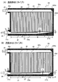
- FIG. 6A and 6B are diagrams illustrating a first modification of a conventional semiconductor module, in which FIG. 6A is a perspective view illustrating an example of arrangement of circuit elements, and FIG. 6B illustrates a configuration of a main part of a water jacket of a cooler.
- FIG. FIG. 7 is a perspective view showing the shape of a water jacket of a type different from the cooler of FIG.
- circuit element portions 3D to 3I, 3Iu, and 3Id in total in seven rows (B1 to B7) in the longitudinal direction of the cooler 2 and two rows in the short direction. Has been placed.
- These circuit element units 3D to 3I, 3Iu, and 3Id can be appropriately combined to be connected to form a plurality of inverter circuits 40 as exemplified in FIG.
- the water jacket 2A is provided with a refrigerant introduction channel 21, a refrigerant discharge channel 22, and a cooling channel 23 on one main surface side.
- a size corresponding to the fin 2C is formed.
- the fin 2C is integrated with the fin base 2B and is disposed toward the water jacket 2A on the fin 2C side.
- the fin base 2B finally integrated with the fin 2C is arrange
- the fin base 2B and the water jacket 2A are joined using, for example, a suitable sealing material (not shown).
- a suitable sealing material not shown
- the cooler 2 provided with water jacket 2A, fin base 2B, and fin 2C can be comprised.
- a guide portion 21Si having an inclination of 60 ° or less is provided at the end portion of the refrigerant flowing into the refrigerant introduction passage 21 from the introduction port 24 and the start end portion of the refrigerant discharge passage 22 through which the refrigerant flows out to the discharge port 25. , 22So.
- the guide portion 21Si has a uniform inclined surface over the entire region facing the cooling flow path 23.
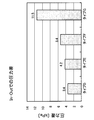
- FIG. 8 is a diagram showing the flow rate of the refrigerant in the semiconductor module of FIGS. 6 and 7 according to the position of the circuit board.
- the graph of FIG. 8 shows, as an example, when the blade fin 2Ca shown in FIG. 4 (A) is arranged in the cooling flow path 23 and a coolant having a flow rate of 10 L / min is caused to flow between the blade fins 2Ca. The flowing refrigerant flow rate is shown.
- each type A, B, C water jacket has a drift characteristic in which the flow velocity distribution is non-uniform for each flow path shape.
- the flow rate of the refrigerant is high on the B1 or B7 side to which the pipe is connected, both of which are 0.15 m. / Sec or more.
- the refrigerant flow rate at the position B7 on the discharge port 25 side is the fastest.
- the refrigerant in the cooling flow path 23 has a drift characteristic in which the flow velocity increases on the discharge port 25 side in the parallel flow path formed by the blade fin 2Ca between the refrigerant introduction flow path 21 and the refrigerant discharge flow path 22. is there.
- circuit elements are arranged in the seventh column on the cooler 2 in addition to twelve circuit element units 3D to 3I in two rows and six columns.
- Different parts can be arranged as the parts 3Iu and 3Id.
- the circuit element units 3Iu and 3Id can be configured as a boost converter circuit using, for example, a predetermined number of IGBTs and FWDs.
- the circuit element units 3Iu and 3Id of the boost converter circuit are connected to the battery and the inverter circuit 40, and the battery voltage is boosted by the circuit element units 3Iu and 3Id.
- the boosted DC current can be converted into an AC current by the inverter circuit 40 and supplied to the three-phase AC motor 41.
- circuit element portions 3Iu and 3Id are relatively easy to dispose at the end of the semiconductor module 10A.
- the refrigerant flowing through the cooling flow path 23 of the cooler 2 has a drift characteristic as described above in which the refrigerant flow rate increases at a position close to the discharge port 25. Moreover, the cooling efficiency by the fins 2 ⁇ / b> C increases as the coolant flows faster through the cooling flow path 23.
- the amount of heat generated when the circuit element units 3D to 3I, 3Iu, and 3Id are driven is not the same, and often varies depending on their functions. In consideration of such circumstances, the circuit element portions 3D to 3I, 3Iu, and 3Id that have a higher amount of heat generated at the time of driving are more easily cooled if arranged on the refrigerant introduction flow path 21 side closer to the discharge port 25. It is possible.
- the circuit element portion with the largest generation loss cannot be disposed at a position close to the discharge port 25, and must be disposed at a position away from the discharge port 25. .
- simply increasing the flow rate of the refrigerant from the inlet 24 results in the flow of more refrigerant than necessary at the portion where the flow velocity is high, and the desired effect can be obtained. Absent.
- the refrigerant flow In order to increase the flow velocity at the low flow velocity portion, the refrigerant flow must be increased and supplied to the cooler, and a high-performance pump is required.
- thermofluid analysis including physical phenomena such as refrigerant flow, heat conduction, and heat transfer. Further, the temperature rise of the refrigerant due to the heat generation in the circuit element units 3D to 3I, 3Iu, 3Id is obtained by analyzing the generated loss generated in the steady operation state.
- the change in the flow rate has a great influence on the cooling capacity in the range where the flow rate of the refrigerant is 0.05 m / s or less, but the change in the cooling capacity with respect to the change in the flow rate is small beyond this range. This tendency also applies to the semiconductor module cooler described in the following embodiments.
- the drift characteristic of the refrigerant is a phenomenon that occurs in the parallel flow path in the cooling flow path 23 sandwiched between the refrigerant introduction flow path 21 and the refrigerant discharge flow path 22.
- the drift characteristics of the fins 2 ⁇ / b> C of the cooling flow path 23 increase as the distance between the fins 2 ⁇ / b> C increases.
- FIG. 9 is a plan view showing the shape of the guide portion of the water jacket used in the semiconductor module of the present invention.
- the introduction port 24 and the discharge port 25 are arranged on the left side wall 2Ab in the same manner as the conventional type A shown in FIG. 6B. Yes.
- the inlet port portion 21a that guides the refrigerant from the inlet port 24 to the refrigerant inlet channel 21 and the outlet port portion 22a for flowing the refrigerant from the refrigerant outlet channel 22 to the outlet port 25 are shown in FIG.
- the introduction port portion 21a and the discharge port portion 22a are formed so as to protrude from the same left side wall 2Ab.
- the refrigerant introduction channel 21 has a guide portion 21Si on the inner surface side of the front side wall 2Aa facing the front side surface (refrigerant inflow surface) of the fin 2C disposed in the cooling channel 23, and the guide portion 21Si
- the width of the refrigerant introduction channel 21 is narrowed toward the terminal direction.
- the type D water jacket 2A is similar to the type A shown in FIG.
- the guide portion 21Si disposed in the refrigerant introduction passage 21 is defined by the inclined surface length x from the end portion and the distance y between the guide portion 21Si and the fin 2C at the end portion of the refrigerant introduction passage 21.
- the water jacket 2A of type G shown in FIG. 9B has a tapered cross section at the inlet port portion 21a that guides the refrigerant to the refrigerant inlet channel 21, and the channel width w1 at the outlet port 25
- the flow path width of the introduction port 21a is changed so that the flow path width w2 at the start end of the refrigerant introduction flow path 21 is narrowed.
- coolant introduction flow path 21, ie, the distance y is the same as that of the type D.
- the refrigerant discharge flow path 22 is formed to have a uniform flow path width w1, while the flow path width w2 is narrower at the start end of the refrigerant introduction flow path 21 and decreases toward the end. It is configured as follows. Therefore, if the guide portion 21Si disposed in the refrigerant introduction channel 21 has an inclined surface with a length x corresponding to the entire region, the inclination angle of the guide portion 21Si is smaller than that of the type D.
- the guide portion 22So is disposed at the start end in the refrigerant discharge passage 22 through which the refrigerant flows out to the discharge port 25, and the rear side surface of the fin 2C (refrigerant). Chamfering is performed at an inclination angle of about 45 ° with respect to the outflow surface. Further, a rear side wall 2Ac is formed in parallel with the rear side surface of the fin 2C toward the downstream side of the refrigerant discharge passage 22. That is, the refrigerant discharge passage 22 has a side wall formed substantially parallel to the rear side surface of the fin 2C over the entire length. Therefore, the pressure loss can be reduced on the downstream side of the heat sink (the refrigerant outflow surface of the fin 2C), and the effect of adjusting the flow rate by the guide portion 21Si can be obtained.
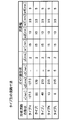
- FIG. 10 is an explanatory view showing the shape of the guide portion and the channel width of the water jacket used for the semiconductor module cooler and the semiconductor module according to the present invention by type.
- the shape of the water jacket of type E, type Ea, type Eb, type F, type Ga and type Gb (inclined surface length x, at the end portion)
- the distance y) and the channel widths (w1, w2) will be described.
- the guide portion 21 ⁇ / b> Si disposed in the refrigerant introduction passage 21 has a length x of 255 mm which is equal to that of the refrigerant introduction passage 21 and at the end of the refrigerant introduction passage 21.
- Type E x and y are the same as those of Type D, 255 mm and 2 mm, respectively, but the flow path width of the introduction port 21a is changed to be narrowed from 15 mm (w1) to 10 mm (w2). Therefore, it is different from that of Type D.
- the guide portion 21 ⁇ / b> Si disposed in the refrigerant introduction passage 21 has an inclined surface length x that is 130 mm shorter than the refrigerant introduction passage 21, and The channel width at the end portion was 2 mm.
- the type Eb guide portion 21Si has an inclined surface in the range of 8 mm (x) in the vicinity of the end portion of the refrigerant introduction flow channel 21 and has a flow channel width of 2 mm. That is, the refrigerant introduction channel 21 has a length of 247 mm and a channel width of 10 mm, and the guide portion 21Si forms an inclined surface of 45 degrees only at the end portion.
- the inclined surface length x and the flow path width (distance y) at the terminal end are the same as those of the type D and type E, and are 255 mm and 2 mm, respectively. Is changed so as to be reduced from 15 mm (w 1) to 8 mm (w 2) at the start end of the refrigerant introduction channel 21. Therefore, the inclination angle of the guide portion 21Si disposed in the refrigerant introduction channel 21 with the inclined surface length x of 255 mm is smaller than that of the type D.
- the guide portion 21Si disposed in the refrigerant introduction channel 21 has an inclined surface length x of 255 mm which is equal to that of the refrigerant introduction channel 21.
- the flow path width (distance y) at the end portion of the refrigerant introduction flow path 21 is 2 mm.
- the introduction port portion 21a having a tapered shape has a width of 5 mm (w2) at the starting end portion of the refrigerant introduction flow channel 21, which is narrower than that of Type F.
- the inclined surface length x of the guide portion 21Si disposed in the refrigerant introduction flow path 21 is 130 mm shorter than the refrigerant introduction flow path 21, and the flow path at the end of the refrigerant introduction flow path 21
- the width (distance y) was 2 mm.
- only the vicinity of the end portion of the refrigerant introduction channel 21 is formed in a range of 3 mm (x), and the channel width (distance y) is 2 mm. That is, the refrigerant introduction flow path 21 has a length of 252 mm and a flow path width of 5 mm, and the guide portion 21 Si forms a 45-degree inclined surface at the end portion.
- the channel shapes of types E to G shown in FIGS. 9 and 10 are all narrowed from w1 to w2 in the inlet port portion 21a upstream of the refrigerant introduction channel 21. Then, as in the case of Type E, Type Ea, Type Eb, Type Ga, and Type Gb, the flow path width (w1, w2) and the guide portion shape (x, y) are changed and combined, respectively, thereby introducing the refrigerant introduction flow path. It is possible to suppress the flow rate of the refrigerant toward the terminal end within 21 to an appropriate level.
- the cooling flow path 23 is formed in a region having a width of 255 mm and a length of 117 mm, in which blade fins 2Ca having a thickness of 1.2 mm, a pitch of 2.1 mm, and a height of 10 mm are arranged. It was assumed that the refrigerant was introduced into the introduction channel 21 at a flow rate of 10 L / min. In addition, by simulating different shapes of the guide portions 21Si, the influence of the difference in the shape of the guide portions 21Si on the flow velocity distribution was confirmed for each of the types D to G.
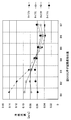
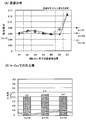
- FIG. 11 is a view showing the flow rate distribution of the refrigerant for each type of position of the circuit board in the semiconductor module cooler of the present invention.
- the flow velocity distribution shown in the figure is the flow velocity between the fins 2C arranged immediately below the center of the substrate of the circuit element units 3D to 3I, 3Iu, and 3Id arranged in seven rows indicated by positions B1 to B7 in FIG. This is a simulation result.
- the flow velocities are shown in order from B1 to B7 from the inlet 24 side toward the end of the refrigerant introduction passage 21.
- the type D to G refrigerant introduction flow passages 21 used in the flow velocity distribution simulation have the guide portion shape and the flow passage width shown in FIG. 10, both of which are the minimum values of the distances between the fins 2C and the guide portions 21Si ( y) is 2 mm.
- the flow path width w1 of the introduction port 24 and the discharge port 25 is constant at 15 mm, and the flow path width w2 at the start end of the refrigerant introduction flow channel 21 is changed in the range of 15 mm to 5 mm.
- the total length of the refrigerant introduction channel 21 is 255 mm, and its height is 10.5 mm.
- the flow velocity decreases on the position B1 side close to the introduction port 24 and the discharge port 25, and the flow velocity on the position B7 side where cooling is necessary. It has improved.
- this flow path form it is possible to obtain substantially uniform drift characteristics by setting the flow path width w2 of the refrigerant introduction flow path 21 to 1/3 of the refrigerant discharge path as in the type G. That is, it was found that the flow velocity distribution depending on the position of the discharge port 25 can be improved by narrowing the flow path width w2.
- the flow velocity at the position B7 farthest from the inlet 24 and the outlet 25 is 0.040 m / s for Type D, 0.053 m / s for Type E, and 0.059 m / s for Type F.
- the type G is 0.064 m / s.
- the flow distribution w2 of the refrigerant introduction passage 21 is narrowed to 5 mm so that the uneven flow distribution is made uniform. It was found that a flow rate distribution with better cooling efficiency can be obtained.
- the power supply for each type of water jacket shown in FIG. 10 having the shape of the guide portion and the width of the flow passage is determined based on the generated loss in the circuit element portions 3D to 3I, 3Iu, and 3Id, respectively. The heat generation state in the semiconductor element can be confirmed.
- FIG. 12 is a diagram showing the heat generation temperature in a steady state for each type of water jacket in FIG. These are all examples of simulation results obtained by the above-described method.
- the positions B1 to B3 of the circuit element units 3D to 3F in three rows from the introduction port 24 side and the circuit element unit It is classified into two groups of positions B4 to B6 of 3G to 3I, and the same size is set in the same group.
- the circuit element units 3Iu and 3Id in the seventh column different generation losses are set in the upstream circuit element unit 3Id and the downstream circuit element unit 3Iu.
- the heat generation temperatures to be compared are the IGBTs arranged on the downstream side of the circuit element portion 3D in the first row (B1) and the circuit element portion 3G in the fourth row (B4), respectively. It is an element. Further, in FIG. 5C, the upstream IGBT element having a larger generation loss among the circuit element portions 3Iu and 3Id in the seventh row (B7) is set as a comparison target.
- the generated loss values set in the circuit element units 3D to 3I, 3Iu, and 3Id in accordance with the respective heat generation amounts are based on the relationship between the refrigerant flow rate, the refrigerant temperature, and the cooling performance, and 3D ⁇ 3G ⁇ 3Iu ⁇ 3Id relationship is set.
- the junction temperature Tj of the circuit element portion 3Id is 142.6 ° C. in the type D, but 135.5 ° C. in the type G, and is reduced by 7.1 ° C. It was observed.
- the junction temperature Tj increases with the change in flow velocity distribution, but is lower than the circuit element unit 3Id having the highest generation loss. All are kept at 123 ° C. or lower. This indicates that a stable cooling performance can be obtained by adjusting the flow velocity distribution corresponding to the loss generated in the circuit element units 3D to 3I, 3Iu, and 3Id.
- the flow velocity in the central portion (B7) of the circuit element portion 3Id having a particularly high loss value is improved by improving the shape of the guide portion such as the width and the inclination.
- the effect of the improvement is great, and the junction temperature of the power semiconductor element can be reduced.
- FIG. 13 is a diagram showing the pressure difference between the refrigerant inlet and outlet in the semiconductor module of the present invention by type.
- the pressure loss can be measured as a refrigerant pressure difference between the inlet 24 and the outlet 25.
- the pressure loss is kept at 6 kPa or less if the flow path width w2 of the refrigerants such as types E to F shown in FIG.
- the flow path width w2 is narrowed to 5 mm like Ga and Gb, it rises to 11.5 kPa. Therefore, it can be seen that when the flow path width w2 at the start end of the refrigerant introduction flow path 21 is narrowed, it is necessary to compensate for the pressure loss by increasing the refrigerant flow rate with a pump that is larger.
- the type G shape is not an unrealistic flow path shape. Furthermore, it is desirable to optimize the pump performance, the temperature of the refrigerant (cooling water), and the flow path width w2 according to the generated loss in the circuit element section.
- the coolant introduction flow path 21 is defined by the inner surface of the bottom wall 2Ae, the inclined surface of the guide portion 21Si, and the front side surface of the fin 2C constituting the heat sink. Then, the cross-sectional area of the refrigerant introduction flow path 21 decreases at a constant rate from the introduction port 24 side toward the end portion, or the same cross-sectional area up to the middle of the refrigerant introduction flow path 21, from there It is formed so as to decrease at a constant rate toward the end portion.
- the semiconductor element can be cooled more uniformly and stably than in the past. Thus, malfunction and destruction due to heat generation of the semiconductor element can be reliably prevented.
- the fin 2C constituting the heat sink has an inlet port portion 21a so that the front side surface thereof is substantially parallel to the inflow direction of the refrigerant flowing in from the inlet port 24 and does not block the refrigerant flow in the refrigerant introduction channel 21. It is arrange
- a separation wall is provided in the refrigerant introduction channel 21 to divide the refrigerant channel into a plurality of channels, so that the channel width of the refrigerant introduction channel 21 is the same as in the first embodiment.
- a cooler that is formed so as to be narrow will be described.
- FIG. 14A and 14B are views showing a water jacket used in the semiconductor module of the present invention, in which FIG. 14A is a plan view showing the shape of the guide portion of the water jacket, and FIG. 14B is a perspective view showing the water jacket of FIG. It is.
- the introduction port 21a and the discharge port 22a are set to have the same flow path width w1 (for example, 15 mm) on the introduction port 24 side and the discharge port 25 side, respectively.
- the introduction port portion 21a for introducing the refrigerant from the introduction port 24 to the refrigerant introduction flow channel 21 and the discharge port portion 22a for allowing the refrigerant to flow out from the refrigerant discharge flow channel 22 to the discharge port 25 are both type D shown in FIG.
- the inlet port 21 a that guides the refrigerant to the refrigerant inlet channel 21 is changed to the channel width w 2 that is narrowed at the start end of the refrigerant inlet channel 21 with respect to the channel width w 1 at the inlet 24.
- 9 is different from the type D and type G shown in FIG. 9 in that an inclined surface is formed only on the inner surface on the discharge port 25 side. That is, the cross section of the introduction port portion 21a is substantially rectangular, and the inclined surface is formed only on the fin 2C side, and the refrigerant introduced from the introduction port 24 is transferred to the side wall (front side wall 2Aa) of the refrigerant introduction channel 21. Inclined to guide towards.
- the refrigerant introduction flow path 21 is formed so as to have the same flow path width w2 by a flat side wall surface having a length x2 from the start end portion to the intermediate position in the downstream direction.
- the channel width is narrowed toward the terminal end by the guide portion 21Si having a length x.
- Guide part 21Si is arrange
- the flow path width of the refrigerant introduction flow path 21 is continuously narrowed at an inclination angle corresponding to the inclined surface length x of the guide portion 21Si so as to increase the refrigerant flow rate.
- the inclined surface of the guide portion 21Si extends to the right side wall 2Ad, and maintains a distance y between the fin 2C and the end portion of the refrigerant introduction flow path 21.
- a separation wall 27 having a height of 10 mm is formed vertically in the coolant introduction channel 21 from the bottom wall 2Ae surface of the water jacket 2A.
- the separation wall 27 is arranged with a length x2 from the starting end portion of the refrigerant introduction flow channel 21 toward the downstream direction, and extends from the start end portion to a substantially intermediate position where the guide portion 21Si is formed. 21 is divided into two. Thereby, the refrigerant introduction flow path 21 is separated into a flow path width w3 between the fin 2C and a flow path width w4 between the front wall 2Aa of the water jacket 2A on the start end side. Become.
- the separation wall 27 is disposed obliquely in the refrigerant introduction channel 21 so that the distance from the fin 2C is equal to the distance y at the downstream end.
- the separation wall 27 is set to 10 mm slightly lower than the height 10.5 mm of the front wall 2Aa of the water jacket 2A, the wall thickness is set to 1.5 mm, the channel width w3 is set to 3.5 mm, and the channel width w4 is set to 5 mm.
- the starting end portion of the refrigerant introduction passage 21 refers to an entrance region where the introduction port portion 21a is connected to the refrigerant introduction passage 21, and is defined by the front side wall 2Aa and the left side wall 2Ab.
- FIG. 15 is a plan view showing a guide portion shape of a water jacket of a type different from the cooler of FIG.
- the length x2 of the separation wall 27 is longer than that of type H (FIG. 14), that is, more than one-half of the length of the refrigerant introduction channel 21.
- the inclined surface length x of the guide portion 21 ⁇ / b> Si is configured to be shorter than half of the length of the refrigerant introduction channel 21.
- the separation wall 27 in the refrigerant introduction channel 21 has substantially the same length x2 as the flat inner wall surface in the refrigerant introduction channel 21.
- the refrigerant flowing toward the upstream side start end portion of the guide portion 21Si is divided into two flow paths at the start end portion of the refrigerant introduction flow path 21, so that the fins 2C are formed on the terminal end side of the refrigerant introduction flow path 21. It becomes possible to increase the flow rate of the refrigerant flowing into the.
- the length of the guide portion 21Si is further shorter than that of the type I, and the guide portion 21Si is connected to the inclined portion of the length x to introduce the refrigerant.
- a flat portion having a length x3 is provided on the terminal end side of the flow path 21. The point where the flat portion of the guide portion 21Si faces the fin 2C at a distance y and the length x2 of the separation wall 27 formed in the refrigerant introduction channel 21 are the length of the flat surface of the refrigerant introduction channel 21.
- Type K is different from Type H and Type I in that it is formed shorter. Note that the water jacket 2A shown in FIGS. 15A and 15B is the same as that of the type H shown in FIG.
- FIG. 16 is an explanatory view showing the shape of the guide portion and the channel width of the water jacket used for the semiconductor module cooler and the semiconductor module of the present invention by type.
- the shape of the guide portion and the channel width of the water jacket 2A of type J and type L will be described.
- the separation wall 27 formed in the refrigerant introduction channel 21 has a length x2 that is 215 mm longer than that of the type I, and the end portion of the separation wall 27 extends from the end position.
- the flow path width is narrowed toward the terminal end by the guide portion 21Si.
- the length x2 of the separation wall 27 is formed to be the same as that of the type K, but the length x of the inclined surface of the guide portion 21Si is 8 mm which is shorter.
- the refrigerant flowing through the cooling flow path 23 has a flow velocity distribution depending on the position of the discharge port 25.
- the separation wall 27 is formed, the flow path of the refrigerant introduction flow path 21 is divided into two, and the flow rate from the refrigerant introduction flow path 21 to the cooling flow path 23 is controlled, so that the outlet 25 Regardless of the position, the drift characteristics of the refrigerant are adjusted.
- the separation wall 27 in the refrigerant introduction flow path 21 is provided so as to partition the refrigerant flow path in the water jacket 2A into two and at the same time narrow the refrigerant flow path on the downstream side of the refrigerant introduction flow path 21.
- a flow channel that directly flows to the end portion of the refrigerant introduction flow channel 21 is formed.
- FIG. 17A is a diagram showing the flow velocity distribution of the refrigerant for each position of the circuit board
- FIG. 17B is a pressure difference between the refrigerant inlet and outlet.
- FIG. The comparison position is the position shown in FIG. 6 (A)
- the ones related to the flow velocity are compared at the positions B1 to B7
- the pressure loss is the pressure difference between the inlet and outlet
- the junction temperature is the first row (B1 3)
- the IGBT element arranged on the downstream side of each of the circuit element units 3D and 3G in the fourth row (B4) and the circuit element unit 3Id having a large generation loss generated in the circuit element unit in the seventh column are targeted. It was.
- the separation wall 27 is disposed up to the central portion in the length direction of the refrigerant introduction channel 21. According to the simulation result for type H shown in FIG. 17A, it can be seen that the flow velocity at positions B5 and B6 is faster than the flow velocity at position B7. This indicates that the flow velocity can be appropriately adjusted by providing the separation wall 27 and adjusting the length x2. That is, when it is desired to particularly improve only the cooling efficiency at the position B5, the length x2 of the separation wall 27 may be extended to the front of the position B5 as in the type H water jacket 2A.
- the length x2 of the separation wall 27 is longer than that of the type H. For this reason, in the simulation result for Type I shown in FIG. 17A, the flow velocity at position B7 is as high as 0.10 m / s as compared with that for Type H. Further, in type J and type K in which the length x2 of the separation wall 27 is long, the flow velocity at position B6 is as fast as 0.07 m / s, and the flow velocity at position B7 is 0.02 m / s in types J and K. About fast.
- the separation wall 27 is extended from the start end portion of the refrigerant introduction passage 21 to a specific position to control the flow velocity distribution of the refrigerant, and the flow velocity at a specific position is adjusted to improve the performance of the cooler. be able to.
- the difference in the flow velocity at the position B7 is 0.121 m / s for the type J and 0.125 m / s for the type K. It can be seen that the pressure loss in Type K is slight but small. Therefore, in order to improve the cooling performance of the circuit element portion 3Id, the shape of the guide portion 21Si is inclined with respect to the heat sink in the range of the length x as in the type K shown in FIG. It is desirable to reduce the cross-sectional area of the refrigerant introduction flow path 21 so as to be parallel in the range, and increase the flow velocity at the end portion of the refrigerant introduction flow path 21 so as to flow to the circuit element portion 3Id.
- Such a shape of the guide portion 21Si is such that a gap is generated between the heat sink and the right side wall 2Ad of the water jacket 2A particularly in the manufacture of the cooler, and the gap must be larger than the interval between the fins 2C. In this case, a decrease in the flow velocity at the position B7 can be suppressed, which is effective.
- the flow velocity at the position B7 is improved. Therefore, the flow velocity distribution in the cooling flow path 23 can be improved to a drift characteristic that does not depend on the discharge port 25. . Further, by increasing the flow rate of the refrigerant flowing to the end portion of the refrigerant introduction flow path 21, the drift in the cooling flow path 23 can be improved. That is, apart from the separation wall 27 that improves the flow velocity distribution of the cooler 2, a guide portion 21 Si having an inclined portion and a flat portion as in the type K is disposed, and at the end portion of the refrigerant introduction passage 21. The intensively increasing flow rate can be reduced. Accordingly, as the semiconductor module 10A shown in FIG. 6A, when the circuit element portion 3Id having a particularly high generated loss is disposed, or when the circuit element portions 3D to 3I, 3Id, 3Iu having different generated losses are disposed. In addition, the cooling performance of the cooler 2 can be improved.
- the refrigerant pressure difference between the inlet 24 and the outlet 25 is 6 kPa or less in any type. Therefore, even if the flow path width w2 at the start end of the refrigerant introduction flow path 21 is not narrowed as much as the cooler of the first embodiment, the flow path of the refrigerant introduction flow path 21 is divided into two to reduce the flow width w2. A flow path shape that enables pressure loss and flow rate adjustment can be realized.
- the flow path width w2 of the refrigerant introduction flow path 21 is limited to a certain extent with respect to the flow path width w1 of the refrigerant discharge flow path 22.
- the separation wall 27 is configured so that the refrigerant is divided into two in the refrigerant introduction flow path 21, whereby the drift distribution can be adjusted, and the semiconductor module cooler with higher cooling efficiency. Was found to be obtained.
- the power supply for each type of water jacket shown in FIG. 16 having the shape and width of the flow jacket is determined based on the loss generated in the circuit element portions 3D to 3I, 3Iu, and 3Id.
- the heat generation state in the semiconductor element can be confirmed.
- FIG. 18 is a diagram showing the heat generation temperature in a steady state for each type of water jacket in FIG. 18A and 18B, the heat generation temperature comparison target is the circuit element portion 3D in the first row (B1) and the circuit element portion 3G in the fourth row (B4) of the semiconductor module shown in FIG. 6A.
- the IGBT elements are arranged on the downstream side of each. Further, in FIG. 18C, the upstream IGBT element having a larger generation loss among the circuit element portions 3Iu and 3Id in the seventh row (B7) is set as a comparison target.
- the type H is 138.3 ° C.
- the type I is 137.3 ° C.
- the type J is 136.7 ° C.
- the temperature is 136.5 ° C. That is, there is a correlation between the improvement result of the flow velocity distribution shown in FIG. 17A and the result of the junction temperature shown in FIG. 18, and in any of the types H to L, the positions B1, B4, and B7. It can be seen that the necessary flow velocity is realized corresponding to the generation loss. Therefore, the flow velocity distribution depending on the position of the discharge port 25 is improved, and the cooling performance of each of the circuit element portions 3D to 3I, 3Iu, 3Id arranged in the water jacket 2A can be improved.
- the guide portion 21Si having the following shape in adjusting the refrigerant flow velocity distribution.
- the change point of the inclination angle that is, the corner portion sandwiched between the flat surface and the inclined surface.
- the guide portion 21Si so as to be located in a range of 1 ⁇ 4 or less from the end portion side.
- the interval between the fin 2C and the guide portion 21Si at the end portion of the refrigerant introduction channel 21 is set to 1 mm or more and 1/3 or less of the maximum channel width of the refrigerant introduction channel 21.
- the separation wall that divides the flow path of the refrigerant 27 also has an inclination angle toward the fin 2C toward the downstream direction.
- FIG. 19 is a view showing a water jacket used in the semiconductor module cooler of the present invention, in which (A) is a plan view showing the shape of a guide portion of the water jacket, and (B) is a water jacket of (A). It is a fragmentary perspective view shown.
- a water jacket 2A of type M shown in FIG. 19A has a shape common to that of type K shown in FIG. 15B, and is an inclined portion having a length x (13 mm) and a flat portion having a length x3 (5 mm).
- the guide portion 21Si having the above is disposed at the end portion of the refrigerant introduction flow path 21.
- the separation wall 27 formed so as to divide the flow path into two from the start end portion of the refrigerant introduction flow path 21 is arranged in parallel to the side surface of the fin 2C in the cooling flow path 23 on the refrigerant inflow side. This is different from the type I and type K water jackets 2A shown in FIG.
- the separation wall 27 disposed in the type M refrigerant introduction flow path 21 has a total length of 215 mm in the refrigerant introduction flow path 21, and the flow path formed with a width of 10 mm is 3.5 mm on the fin 2C side,
- the front wall 2Aa is provided with a width of 5 mm so as to be divided into two flow paths. Further, at the end portion on the downstream side of the separation wall 27, the thickness of the separation wall 27 itself was maintained (1.5 mm), and it was bent at an angle of about 45 ° C. to a position where the distance from the fin 2C became 2 mm. A tip portion 27a is formed.
- the upstream end of the separation wall 27 is located in the entrance region of the refrigerant introduction channel 21.
- the tip portion 27a of the separation wall 27 By forming the tip portion 27a of the separation wall 27 in this way, not only the flow rate of the refrigerant flowing from the introduction port 24 is increased, but also the flow rate of the refrigerant flowing into the fin 2C facing the tip portion 27a is increased. it can. Therefore, the flow rate of the refrigerant toward the end portion in the refrigerant introduction flow path 21 is increased, and the cooling effect on the circuit element portion arranged at the position of the tip portion 27a of the separation wall 27 can be enhanced.
- the flow rate of the refrigerant toward the end portion in the refrigerant introduction flow path 21 is improved, and the generated loss in the circuit element units 3D to 3I, 3Iu, and 3Id arranged in the semiconductor module 10A shown in FIG. Accordingly, it is possible to appropriately improve the cooling performance of the cooler 2.
- FIG. 20 is a partial plan view showing the shape of the introduction path of a type N water jacket different from the cooler of FIG.
- the semiconductor module cooler including the type N water jacket shown in FIG. 20 one plate-like separation wall 27 is arranged so as to divide the flow path into two from the start end portion of the refrigerant introduction flow path 21.
- the separation wall 27 is arranged in parallel to the front side wall 2Aa of the water jacket 2A.
- the separation wall 27 is configured to be shorter than the length of the fin 2C side on the front wall 2Aa side of the water jacket 2A, and the cross-sectional shape when viewed in plan is substantially trapezoidal. This is because the flow of the refrigerant flowing into the refrigerant introduction flow path 21 is made smooth so that unnecessary vortices are not generated.
- the separation wall 27 is formed in a shape that does not cause unnecessary resistance to the flow of the refrigerant by chamfering the corners of the separation wall 27 based on the rectangular parallelepiped shape shown in FIG. desirable.
- FIG. 21A is a diagram showing the flow velocity distribution of the refrigerant for each position of the circuit board
- FIG. 21B is a refrigerant inlet and outlet for each semiconductor module cooler of FIGS. It is a figure which shows the pressure difference in.
- FIG. 6A shows the flow velocity distribution of the refrigerant with the circuit board positions B1 to B7 shown in FIG.
- the flow velocity at position B7 is 0.123 m / s for Type M and 0.127 m / s for Type N. That is, looking at the flow velocity distributions of type M and type N, the flow velocity at circuit board position B6 can be made higher than that at type K without reducing the flow velocity at final position B7.
- the pressure difference between the introduction port 24 and the discharge port 25 is suppressed to a low pressure loss of 6 kPa or less in any type. Therefore, the load on the pump performance can be reduced, and the flow rate of the refrigerant can be easily increased, so that the cooling performance can be further improved.
- a separation wall extending in the downstream direction of the refrigerant from the start end portion thereof is arranged in the refrigerant introduction flow path 21 so as to be separated from one side surface of the fin 2 ⁇ / b> C in parallel.
- the separation wall 27 is arranged in parallel with the fins 2C, so that not only the ease in manufacturing technology can be obtained, but also the drainage is reduced. It is also possible to improve the flow rate at the position B6 by suppressing the flow rate of the refrigerant at the positions B1 to B4 on the outlet 25 side.
- each semiconductor element of the semiconductor module can be cooled uniformly and stably, and the cooling efficiency can be improved.
- FIG. 22 is a diagram showing the performance of the water jacket of FIGS. 15, 19 and 20 by type.
- the junction temperature of the semiconductor element to be maintained is lower than the junction temperature in the circuit element units 3Id and 3Iu.
- the junction temperature at position 3Id shown in FIG. 22C is 136.5 ° C. for type K, 135.9 ° C. for type M, and 135.8 ° C. for type N.
- N is lower, which is improved by arranging the separation wall 27 parallel to the side wall of the fin 2C. This effect does not depend on the presence or absence of the tip portion 27a inclined at 45 ° at the end portion of the separation wall 27 of type M.
- the separation wall 27 is arranged in parallel with the fins 2C, and the shape of the separation wall 27 is adjusted to a flow rate distribution by adjusting the flow velocity distribution by simply forming a trapezoid or chamfered shape without bending the tip 27a.
- the cooling performance can be improved.
Abstract
Description
図4は、2通りのフィンの形状を説明する図であって、(A)はブレードフィンを示す斜視図、(B)はコルゲートフィンを示す斜視図である。 Next, the shape of the
4A and 4B are diagrams for explaining the shapes of two types of fins. FIG. 4A is a perspective view showing a blade fin, and FIG. 4B is a perspective view showing a corrugated fin.
このようなブレードフィン2Ca、あるいはコルゲートフィン2Cbの形状をもつフィン2Cは、例えば図2に示したように、フィンベース2Bと一体化してフィン2C側のウォータージャケット2Aに向けて配置される。フィン2Cは、その先端とウォータージャケット2Aの底壁2Aeとの間に一定のクリアランスCが存在するような寸法(高さ)に形成される。 Although FIG. 4A illustrates the blade fin 2Ca, the corrugated fin 2Cb shown in FIG. 4B can also be used.
The
フィン2C及びフィンベース2Bは、ウォータージャケット2Aと同様に、例えばアルミニウム、アルミニウム合金、銅、銅合金等の金属材料を用いて形成することができる。フィン2Cは、上述したブレードフィン2Caやコルゲートフィン2Cb等以外にも例えば金属材料を用いて形成された所定のピンや板体を金属製の基材26に接合することによって形成することができる。 Moreover, the external shape of the heat sink composed of the
The
このような基板31上に搭載される半導体素子32,33としては、ここではパワー半導体素子を用いている。一例として、図5に示すように、一方の半導体素子32をフリーホイールダイオード(Free Wheeling Diode:FWD)とし、他方の半導体素子33を絶縁ゲートバイポーラトランジスタ(Insulated Gate Bipolar Transistor:IGBT)とすることができる。 FIG. 5 is a diagram illustrating an example of a power conversion circuit configured as a semiconductor module.
Here, power semiconductor elements are used as the
図5では、直流電流を交流電流に変換して三相交流モータ41に供給するインバータ回路40を例示している。このインバータ回路40は、U相、V相、W相の三相についてそれぞれ、IGBTである半導体素子33と、FWDである半導体素子32とのブリッジ回路を備える。半導体素子33のスイッチング制御を行うことで、直流電流を交流電流に変換し、三相交流モータ41を駆動することができるようになっている。 In the
FIG. 5 illustrates an
図8のグラフは、一例として図4(A)に示すブレードフィン2Caを冷却用流路23内に配置して、導入口24から流量10L/minの冷媒を流したとき、ブレードフィン2Ca間を流れる冷媒流速を示している。 FIG. 8 is a diagram showing the flow rate of the refrigerant in the semiconductor module of FIGS. 6 and 7 according to the position of the circuit board.
The graph of FIG. 8 shows, as an example, when the blade fin 2Ca shown in FIG. 4 (A) is arranged in the
こうした事情を考慮すると、回路素子部3D~3I、及び3Iu、3Idのうちその駆動時に発生する熱量が高いものほど排出口25に近い冷媒導入流路21側に配置すれば、より容易に冷却することが可能である。 In addition, the amount of heat generated when the circuit element units 3D to 3I, 3Iu, and 3Id are driven is not the same, and often varies depending on their functions.
In consideration of such circumstances, the circuit element portions 3D to 3I, 3Iu, and 3Id that have a higher amount of heat generated at the time of driving are more easily cooled if arranged on the refrigerant
(第1の実施の形態)
第1の実施の形態では、半導体モジュールにおける偏流を調整するため、冷媒導入流路21の幅を狭くした冷却器2について説明する。 The following embodiments have been improved so as to adjust the flow velocity distribution of the semiconductor module in which the
(First embodiment)
In the first embodiment, a description will be given of the
ここでは、図9に示すタイプDおよびタイプGの他に、タイプE、タイプEa、タイプEb、タイプF、タイプGaおよびタイプGbのウォータージャケットのガイド部形状(傾斜面長さx、終端部での距離y)と流路幅(w1,w2)について説明する。タイプDのウォータージャケット2Aでは、冷媒導入流路21に配置されるガイド部21Siは、その長さxが冷媒導入流路21と等しい255mmであって、かつ冷媒導入流路21の終端部での流路幅(距離y)を2mmとする形状を有している。なお、導入口部21aと排出口部22aの流路幅は、いずれも同じw1(=15mm)に形成されている。 FIG. 10 is an explanatory view showing the shape of the guide portion and the channel width of the water jacket used for the semiconductor module cooler and the semiconductor module according to the present invention by type.
Here, in addition to the type D and type G shown in FIG. 9, the shape of the water jacket of type E, type Ea, type Eb, type F, type Ga and type Gb (inclined surface length x, at the end portion) The distance y) and the channel widths (w1, w2) will be described. In the type
同図に示す流速分布は、図6において位置B1~B7で示した7列に配置された回路素子部3D~3I、3Iu,3Idの基板中央部直下に配置されたフィン2C間での流速をシミュレーションした結果である。ここでは、導入口24側から冷媒導入流路21の終端部に向けてB1~B7まで順に流速を示している。 FIG. 11 is a view showing the flow rate distribution of the refrigerant for each type of position of the circuit board in the semiconductor module cooler of the present invention.
The flow velocity distribution shown in the figure is the flow velocity between the
シミュレーションにおいて、回路素子部3D等に与える発生損失として、上述した図6(A)に示すように、導入口24側より3列ずつ回路素子部3D~3Fの位置B1~B3と、回路素子部3G~3Iの位置B4~B6の2グループに分類して、同じグループでは同じ大きさに設定している。また、7列目の回路素子部3Iu,3Idでは、上流側の回路素子部3Idと下流側の回路素子部3Iuで、互いに異なる発生損失を設定している。図12(A),(B)における発熱温度の比較対象は、それぞれ1列目(B1)の回路素子部3D、4列目(B4)の回路素子部3Gのそれぞれ下流側に配置されたIGBT素子としている。また、同図(C)では7列目(B7)の回路素子部3Iu,3Idのうち、発生損失のより大きい上流側のIGBT素子を比較対象とした。さらに、回路素子部3D~3I,3Iu,3Idにそれぞれの発熱量に応じて設定している発生損失値は、冷媒流速と冷媒温度及び冷却性能との関係に基づいて、3D<3G<3Iu<3Idの関係に設定している。 FIG. 12 is a diagram showing the heat generation temperature in a steady state for each type of water jacket in FIG. These are all examples of simulation results obtained by the above-described method.
In the simulation, as the generated loss given to the circuit element unit 3D and the like, as shown in FIG. 6A described above, the positions B1 to B3 of the circuit element units 3D to 3F in three rows from the
(第2の実施の形態)
第2の実施の形態では、冷媒導入流路21内に分離壁を設けて冷媒の流路を複数に分割することにより、第1の実施の形態のように冷媒導入流路21の流路幅を狭く形成するようにした冷却器について説明する。 The
(Second Embodiment)
In the second embodiment, a separation wall is provided in the
図15(A)に示すタイプIのウォータージャケット2Aは、分離壁27の長さx2がタイプH(図14)のものより長く、すなわち冷媒導入流路21の長さの2分の1以上の長さに形成され、かつガイド部21Siの傾斜面長さxが冷媒導入流路21の長さの半分以下まで短く構成されている。そして、冷媒導入流路21内の分離壁27は、冷媒導入流路21内の平坦な内壁面とほぼ同じ長さx2を有している。これにより、ガイド部21Siの上流側始端部方向に向かって流れる冷媒は、冷媒導入流路21の始端部で2つの流路に分割されるため、冷媒導入流路21の終端部側でフィン2Cに流入する冷媒の流量を増加することが可能になる。 FIG. 15 is a plan view showing a guide portion shape of a water jacket of a type different from the cooler of FIG.
In the type
ここでは、図14に示すタイプH、および図15(A),(B)に示すタイプI、タイプKの他に、タイプJ、タイプLのウォータージャケット2Aのガイド部形状と流路幅について説明する。タイプJのウォータージャケット2Aでは、冷媒導入流路21内に形成される分離壁27は、その長さx2がタイプIのものより長い215mmであって、この分離壁27の端部位置から終端部までの流路幅は、ガイド部21Siによって終端方向に向かって狭められている。また、タイプLのものでは、分離壁27の長さx2はタイプKと同じ長さに形成されているが、ガイド部21Siの傾斜面の長さxが、さらに短い8mmとなっている。 FIG. 16 is an explanatory view showing the shape of the guide portion and the channel width of the water jacket used for the semiconductor module cooler and the semiconductor module of the present invention by type.
Here, in addition to the type H shown in FIG. 14 and the types I and K shown in FIGS. 15A and 15B, the shape of the guide portion and the channel width of the
比較位置は図6(A)に示した位置とし、流速に関わるものをB1~B7の位置において比較し、圧力損失は導入口と排出口の圧力差とし、ジャンクション温度については1列目(B1)、4列目(B4)の回路素子部3D,3Gのそれぞれ下流側に配置されたIGBT素子と、7列目の回路素子部で発生する発生損失の大きい回路素子部3Idの3箇所を対象とした。 17A is a diagram showing the flow velocity distribution of the refrigerant for each position of the circuit board, and FIG. 17B is a pressure difference between the refrigerant inlet and outlet. FIG.
The comparison position is the position shown in FIG. 6 (A), the ones related to the flow velocity are compared at the positions B1 to B7, the pressure loss is the pressure difference between the inlet and outlet, and the junction temperature is the first row (B1 3) The IGBT element arranged on the downstream side of each of the
(第3の実施の形態)
つぎに、第3の実施の形態として傾斜のない分離壁27を設けたウォータージャケット2Aについて説明する。 Further, from the simulation results, it can be seen that it is preferable to use the guide portion 21Si having the following shape in adjusting the refrigerant flow velocity distribution. For example, as in types J and K, in the longitudinal direction of the
(Third embodiment)
Next, a
図20に示すタイプNのウォータージャケットを備える半導体モジュール用冷却器では、1枚の板状の分離壁27が、冷媒導入流路21の始端部から流路を2分するように配置される。ここでも、図19のタイプMと同様に、分離壁27はウォータージャケット2Aの前側壁2Aaに対して平行に配置されている。また、この分離壁27はウォータージャケット2Aの前側壁2Aa側で、フィン2C側の長さより短く構成され、その平面視したときの断面形状は略台形となっている。これは、冷媒導入流路21内に流入する冷媒の流れを円滑なものとして、不要な渦を発生させないようにするためである。 FIG. 20 is a partial plan view showing the shape of the introduction path of a type N water jacket different from the cooler of FIG.
In the semiconductor module cooler including the type N water jacket shown in FIG. 20, one plate-
タイプK,M,Nの半導体モジュール用冷却器における回路素子部3D~3I下の冷却用流路23では、その圧力損失の関係から安定した流速が得られるため、回路素子部3D~3Iに配置される半導体素子のジャンクション温度は、回路素子部3Id,3Iuにおけるジャンクション温度よりも低い値を保っている。他方、図22(C)に示す位置3Idでのジャンクション温度は、タイプKで136.5℃、タイプMで135.9℃、タイプNで135.8℃であり、タイプKよりもタイプM,Nの方が低く、分離壁27をフィン2Cの側壁に平行に配置したことによって改善されている。この効果は、タイプMの分離壁27終端部の45°に傾斜した先端部27aの有無には依存していない。 FIG. 22 is a diagram showing the performance of the water jacket of FIGS. 15, 19 and 20 by type.
In the cooling
範囲において種々の変更を加えることが可能である。
上記については単に本発明の原理を示すものである。さらに、多数の変形、変更が当業者にとって可能であり、本発明は上記に示し、説明した正確な構成および応用例に限定されるものではなく、対応するすべての変形例および均等物は、添付の請求項およびその均等物による本発明の範囲とみなされる。 The present invention is not limited to the above embodiment, and various modifications can be made without departing from the spirit of the present invention.
The above merely illustrates the principle of the present invention. In addition, many modifications and changes can be made by those skilled in the art, and the present invention is not limited to the precise configuration and application shown and described above, and all corresponding modifications and equivalents may be And the equivalents thereof are considered to be within the scope of the invention.
2A ウォータージャケット
2B フィンベース
2C フィン
10,10A 半導体モジュール
21 冷媒導入流路
21a 導入口部
21Si,22So ガイド部
22 冷媒排出流路
22a 排出口部
23 冷却用流路
24 導入口
25 排出口
26 基材
27 分離壁
27a 先端部
3A~3I,3Iu,3Id 回路素子部
31 基板
31a 絶縁基板
31b,31c 導体パターン
32,33 半導体素子
34,35 接合層
40 インバータ回路
41 三相交流モータ
C クリアランス
B1~B7 位置 DESCRIPTION OF
Claims (16)
- ウォータージャケットに外部から冷媒を供給して、その外面に配置される半導体素子を冷却する半導体モジュール用冷却器において、
前記半導体素子と熱的に接続されるヒートシンクと、
前記ウォータージャケット内に、冷媒導入口から延在され、かつ前記ヒートシンクの一の側面に向かって前記冷媒を誘導するための傾斜面を有するガイド部が配置された第1流路と、
前記第1流路と並列して前記ウォータージャケット内に配置され、冷媒排出口に延在され、かつ前記ヒートシンクの他の側面に平行な側壁が形成された第2流路と、
前記ウォータージャケット内の前記第1流路と前記第2流路とを連通する位置に形成された第3流路と、
を備え、前記冷媒導入口と前記冷媒排出口が前記ウォータージャケットの同一壁面に形成され、前記ヒートシンクが前記第3流路内に配置されていることを特徴とする半導体モジュール用冷却器。 In a semiconductor module cooler for supplying a coolant to the water jacket from the outside and cooling a semiconductor element disposed on the outer surface thereof,
A heat sink thermally connected to the semiconductor element;
A first flow path in which a guide portion extending from a refrigerant introduction port and having an inclined surface for guiding the refrigerant toward one side surface of the heat sink is disposed in the water jacket;
A second flow path disposed in the water jacket in parallel with the first flow path, extending to the coolant discharge port, and having a side wall formed parallel to the other side surface of the heat sink;
A third channel formed at a position communicating the first channel and the second channel in the water jacket;
The semiconductor module cooler is characterized in that the coolant introduction port and the coolant discharge port are formed on the same wall surface of the water jacket, and the heat sink is disposed in the third flow path. - 前記第1流路の前記冷媒導入口側の端部での断面積が、前記第2流路の前記冷媒排出口側の端部での断面積より小さく、かつ前記ガイド部は、前記冷媒導入口から前記ヒートシンクの一の側面に接するまでの間で前記第1流路の断面積を低減するように構成されていることを特徴とする請求の範囲第1項記載の半導体モジュール用冷却器。 The cross-sectional area at the end of the first flow path on the refrigerant inlet side is smaller than the cross-sectional area at the end of the second flow path on the refrigerant discharge port side, and the guide section 2. The cooler for a semiconductor module according to claim 1, wherein the cooler is configured to reduce a cross-sectional area of the first flow path from a mouth to a side surface of the heat sink.
- 前記第1流路内には、前記ヒートシンクの一の側面から離間して、前記第1流路の始端部から前記冷媒の下流方向に延長形成された分離壁が配置されていることを特徴とする請求の範囲第1項記載の半導体モジュール用冷却器。 In the first flow path, a separation wall extending from the start end portion of the first flow path in the downstream direction of the refrigerant is disposed apart from one side surface of the heat sink. The cooler for a semiconductor module according to claim 1.
- 前記第1流路の流路幅は、前記冷媒導入口側で前記第2流路の幅と等しく、かつ前記第1流路内の下流側でその断面積が連続して低減するように構成されていることを特徴とする請求の範囲第1項記載の半導体モジュール用冷却器。 The flow path width of the first flow path is equal to the width of the second flow path on the refrigerant inlet side, and the cross-sectional area continuously decreases on the downstream side in the first flow path. The cooler for a semiconductor module according to claim 1, wherein the cooler is for semiconductor modules.
- 前記冷媒導入口から前記第1流路に冷媒を導く導入口部と、前記第2流路から冷媒を前記冷媒排出口に流出するための排出口部とをさらに備え、前記導入口部の前記ヒートシンク側の壁が前記第1流路の側壁に向かって冷媒を誘導するための傾斜面を有することを特徴とする請求の範囲第1項記載の半導体モジュール用冷却器。 An inlet port that guides the refrigerant from the refrigerant inlet to the first flow path; and a discharge port part for discharging the refrigerant from the second flow path to the refrigerant outlet. 2. The cooler for a semiconductor module according to claim 1, wherein the wall on the heat sink side has an inclined surface for guiding the refrigerant toward the side wall of the first flow path.
- 前記分離壁は、前記第1流路の長さの2分の1以上の長さであり、かつ前記ガイド部の傾斜角度とは異なる傾斜をもって前記ヒートシンクの一の側面に向かって前記冷媒を誘導する傾斜面を有することを特徴とする請求の範囲第3項記載の半導体モジュール用冷却器。 The separation wall has a length equal to or more than a half of the length of the first flow path, and guides the refrigerant toward one side surface of the heat sink with an inclination different from an inclination angle of the guide portion. 4. The semiconductor module cooler according to claim 3, further comprising an inclined surface.
- 前記分離壁は、前記第1流路の長さの2分の1以上の長さであり、かつ前記ヒートシンクの一の側面と平行に配置されていることを特徴とする請求の範囲第3項記載の半導体モジュール用冷却器。 4. The separation wall according to claim 3, wherein the separation wall has a length of one half or more of a length of the first flow path and is disposed in parallel with one side surface of the heat sink. The cooler for semiconductor modules as described.
- 前記分離壁は、前記ウォータージャケットの底面から当該流路の高さに対して50%以上の高さになるよう配置されていることを特徴とする請求の範囲第3項記載の半導体モジュール用冷却器。 4. The cooling for a semiconductor module according to claim 3, wherein the separation wall is disposed so as to have a height of 50% or more with respect to the height of the flow path from the bottom surface of the water jacket. vessel.
- 前記ガイド部は、前記ヒートシンクの一の側面に向かって傾斜する一の面、及び当該一の側面に連続する他の面を含むことを特徴とする請求の範囲第3項記載の半導体モジュール用冷却器。 4. The cooling for a semiconductor module according to claim 3, wherein the guide portion includes one surface inclined toward one side surface of the heat sink and another surface continuous with the one side surface. vessel.
- 前記ガイド部の前記他の面は、前記ヒートシンクの一の側面に対し平行であることを特徴とする請求の範囲第9項記載の半導体モジュール用冷却器。 10. The semiconductor module cooler according to claim 9, wherein the other surface of the guide portion is parallel to one side surface of the heat sink.
- 前記ガイド部の前記他の面は、前記冷媒導入口から前記第1流路の終端部に至る流路長の1/4以下の長さで当該終端部側に形成され、かつ前記他の面と前記ヒートシンクの一の側面は、前記第1流路の最大流路幅の1/3以下だけ離間していることを特徴とする請求の範囲第9項記載の半導体モジュール用冷却器。 The other surface of the guide portion is formed on the end portion side with a length equal to or less than ¼ of the flow path length from the refrigerant introduction port to the end portion of the first flow path, and the other surface. 10. The cooler for a semiconductor module according to claim 9, wherein one side surface of the heat sink is separated by 1/3 or less of the maximum flow path width of the first flow path.
- 前記半導体モジュール用冷却器は、その外面に前記冷媒の導入方向に沿って発熱特性の異なる複数の半導体素子が配置され、
前記第1流路内で前記冷媒導入口から下流方向に当該発熱特性が最高である半導体素子の配置領域まで分離壁を配置したことを特徴とする請求の範囲第1項記載の半導体モジュール用冷却器。 The semiconductor module cooler is provided with a plurality of semiconductor elements having different heat generation characteristics along an introduction direction of the refrigerant on an outer surface thereof,
2. The cooling for a semiconductor module according to claim 1, wherein a separation wall is arranged in the first flow path from the refrigerant inlet to the arrangement area of the semiconductor element having the highest heat generation characteristic in the downstream direction. vessel. - 前記ヒートシンクの外形が直方体であることを特徴とする請求の範囲第1項記載の半導体モジュール用冷却器。 The semiconductor module cooler according to claim 1, wherein the heat sink has a rectangular parallelepiped shape.
- 前記ヒートシンクが、前記第3流路の底面から離隔して配置されたことを特徴とする請求の範囲第1項記載の半導体モジュール用冷却器。 The semiconductor module cooler according to claim 1, wherein the heat sink is disposed apart from the bottom surface of the third flow path.
- 前記ウォータージャケットは、前記ヒートシンクを有するフィンベースにより前記冷媒導入口及び前記冷媒排出口を除いて封止されていることを特徴とする請求の範囲第1項記載の半導体モジュール用冷却器。 2. The semiconductor module cooler according to claim 1, wherein the water jacket is sealed by a fin base having the heat sink except for the refrigerant inlet and the refrigerant outlet.
- ウォータージャケットに外部から冷媒を供給して、その外面に配置された半導体素子を冷却する冷却器を備えた半導体モジュールにおいて、
前記半導体素子と熱的に接続されたヒートシンクと、
前記ウォータージャケット内に、冷媒導入口から延在され、かつ前記ヒートシンクの一の側面に向かって前記冷媒を誘導するための傾斜面を有するガイド部が配置された第1流路と、
前記第1流路と並列して前記ウォータージャケット内に配置され、冷媒排出口に延在され、かつ前記ヒートシンクの他の側面に平行な側壁が形成された第2流路と、
前記ウォータージャケット内の前記第1流路と前記第2流路とを連通する位置に形成された第3流路と、
を備え、前記冷媒導入口と前記冷媒排出口が前記ウォータージャケットの同一壁面に形成され、前記ヒートシンクが前記第3流路内に配置されていることを特徴とする半導体モジュール。 In a semiconductor module comprising a cooler for supplying a coolant to the water jacket from the outside and cooling a semiconductor element disposed on the outer surface thereof,
A heat sink thermally connected to the semiconductor element;
A first flow path in which a guide portion extending from a refrigerant introduction port and having an inclined surface for guiding the refrigerant toward one side surface of the heat sink is disposed in the water jacket;
A second flow path disposed in the water jacket in parallel with the first flow path, extending to the coolant discharge port, and having a side wall formed parallel to the other side surface of the heat sink;
A third channel formed at a position communicating the first channel and the second channel in the water jacket;
The semiconductor module, wherein the coolant introduction port and the coolant discharge port are formed on the same wall surface of the water jacket, and the heat sink is disposed in the third flow path.
Priority Applications (4)
| Application Number | Priority Date | Filing Date | Title |
|---|---|---|---|
| CN201280018603.3A CN103503131B (en) | 2011-04-26 | 2012-04-16 | Semiconductor module cooler and semiconductor module |
| EP12776276.3A EP2704191B1 (en) | 2011-04-26 | 2012-04-16 | Cooler for semiconductor module |
| US14/110,856 US9237676B2 (en) | 2011-04-26 | 2012-04-16 | Semiconductor module cooler and semiconductor module |
| JP2013512011A JP5692368B2 (en) | 2011-04-26 | 2012-04-16 | Semiconductor module cooler and semiconductor module |
Applications Claiming Priority (2)
| Application Number | Priority Date | Filing Date | Title |
|---|---|---|---|
| JP2011-098700 | 2011-04-26 | ||
| JP2011098700 | 2011-04-26 |
Publications (1)
| Publication Number | Publication Date |
|---|---|
| WO2012147544A1 true WO2012147544A1 (en) | 2012-11-01 |
Family
ID=47072066
Family Applications (1)
| Application Number | Title | Priority Date | Filing Date |
|---|---|---|---|
| PCT/JP2012/060215 WO2012147544A1 (en) | 2011-04-26 | 2012-04-16 | Cooler for semiconductor module, and semiconductor module |
Country Status (5)
| Country | Link |
|---|---|
| US (1) | US9237676B2 (en) |
| EP (1) | EP2704191B1 (en) |
| JP (1) | JP5692368B2 (en) |
| CN (1) | CN103503131B (en) |
| WO (1) | WO2012147544A1 (en) |
Cited By (16)
| Publication number | Priority date | Publication date | Assignee | Title |
|---|---|---|---|---|
| JP2014116404A (en) * | 2012-12-07 | 2014-06-26 | Mitsubishi Electric Corp | Cooling apparatus |
| JP2014135457A (en) * | 2013-01-11 | 2014-07-24 | Honda Motor Co Ltd | Cooler for semiconductor module, and semiconductor module |
| WO2015079643A1 (en) * | 2013-11-28 | 2015-06-04 | 富士電機株式会社 | Method of manufacturing cooler for semiconductor module, cooler for semiconductor module, semiconductor module, and electrically driven vehicle |
| JP2018041978A (en) * | 2014-08-06 | 2018-03-15 | 富士電機株式会社 | Semiconductor device |
| JP2019052770A (en) * | 2017-09-12 | 2019-04-04 | セイコーエプソン株式会社 | Heat exchange device, cooling device, and projector |
| WO2019180762A1 (en) | 2018-03-19 | 2019-09-26 | 三菱電機株式会社 | Liquid-cooled cooler |
| WO2020059511A1 (en) * | 2018-09-21 | 2020-03-26 | 株式会社デンソー | Cooler |
| JP2020077679A (en) * | 2018-11-06 | 2020-05-21 | 富士電機株式会社 | Semiconductor module and vehicle |
| JP2020088109A (en) * | 2018-11-21 | 2020-06-04 | 三井化学株式会社 | Cooler and structure |
| US10950522B2 (en) * | 2017-02-13 | 2021-03-16 | Shindengen Electric Manufacturing Co., Ltd. | Electronic device |
| JP7074270B1 (en) | 2022-01-19 | 2022-05-24 | 富士電機株式会社 | Semiconductor device |
| JP7111268B1 (en) | 2022-01-19 | 2022-08-02 | 富士電機株式会社 | Coolers and semiconductor equipment |
| JP7120480B1 (en) | 2022-01-19 | 2022-08-17 | 富士電機株式会社 | Coolers and semiconductor equipment |
| JP7342811B2 (en) | 2020-07-10 | 2023-09-12 | 株式会社豊田自動織機 | Cooler |
| JP7367418B2 (en) | 2019-09-13 | 2023-10-24 | 富士電機株式会社 | Semiconductor modules and vehicles |
| WO2023248989A1 (en) * | 2022-06-20 | 2023-12-28 | ニデック株式会社 | Cooling device and semiconductor device |
Families Citing this family (37)
| Publication number | Priority date | Publication date | Assignee | Title |
|---|---|---|---|---|
| US9190344B2 (en) * | 2007-11-26 | 2015-11-17 | Kabushiki Kaisha Toyota Jidoshokki | Liquid-cooled-type cooling device |
| JP5563383B2 (en) * | 2010-06-21 | 2014-07-30 | 日立オートモティブシステムズ株式会社 | Power converter |
| US8982558B2 (en) * | 2011-06-24 | 2015-03-17 | General Electric Company | Cooling device for a power module, and a related method thereof |
| CN104145333B (en) * | 2012-04-16 | 2018-02-02 | 富士电机株式会社 | Semiconductor device and semiconductor device cooler |
| US8847384B2 (en) | 2012-10-15 | 2014-09-30 | Toyota Motor Engineering & Manufacturing North America, Inc. | Power modules and power module arrays having a modular design |
| EP2824703B1 (en) * | 2012-10-29 | 2022-06-29 | Fuji Electric Co., Ltd. | Semiconductor device |
| CN104423503A (en) * | 2013-08-28 | 2015-03-18 | 英业达科技有限公司 | Server |
| DE112014000898T5 (en) * | 2013-09-05 | 2015-11-26 | Fuji Electric Co., Ltd. | The power semiconductor module |
| CN106298688B (en) * | 2015-05-28 | 2018-11-06 | 台达电子工业股份有限公司 | Encapsulation type power circuitry module |
| EP3306659B1 (en) * | 2015-06-03 | 2021-08-04 | Mitsubishi Electric Corporation | Liquid-cooled cooler, and manufacturing method for radiating fin in liquid-cooled cooler |
| DE102015212720A1 (en) * | 2015-07-08 | 2017-01-12 | Robert Bosch Gmbh | Power semiconductor device with a cooling device |
| CN104977245A (en) * | 2015-07-14 | 2015-10-14 | 北京瑞尔腾普科技有限公司 | Environmental test device |
| CN204967631U (en) * | 2015-08-04 | 2016-01-13 | 中山大洋电机股份有限公司 | Cooling system of expanded dc -to -ac converter and machinery assembly thereof |
| US9443786B1 (en) * | 2015-08-19 | 2016-09-13 | Ac Propulsion, Inc. | Packaging and cooling method and apparatus for power semiconductor devices |
| FR3043880B1 (en) * | 2015-11-13 | 2017-12-29 | Valeo Systemes De Controle Moteur | HOUSING FOR ELECTRICAL EQUIPMENT |
| US10388589B2 (en) * | 2015-11-25 | 2019-08-20 | Mitsubishi Electric Corporation | Semiconductor device, inverter device, and vehicle |
| EP3379908B1 (en) * | 2017-03-24 | 2020-04-29 | EKWB d.o.o. | Method for manufacturing a fluid-based cooling element and fluid-based cooling element |
| US10191521B2 (en) * | 2017-05-25 | 2019-01-29 | Coolanyp, LLC | Hub-link liquid cooling system |
| US10892208B2 (en) * | 2017-10-19 | 2021-01-12 | Beijing E. Motor Advance Co. Ltd. | Heat dissipation apparatus and method for power semiconductor devices |
| JP6939481B2 (en) * | 2017-11-30 | 2021-09-22 | 富士通株式会社 | Cooling jackets and electronics |
| JP7205071B2 (en) | 2018-04-02 | 2023-01-17 | 富士電機株式会社 | Chillers, semiconductor modules and vehicles |
| CN108617148A (en) * | 2018-06-06 | 2018-10-02 | 张家港首驱动力科技有限公司 | A kind of heat sink of Trapezoidal water channel |
| US11467637B2 (en) | 2018-07-31 | 2022-10-11 | Wuxi Kalannipu Thermal Management Technology Co., Ltd. | Modular computer cooling system |
| JP7087850B2 (en) * | 2018-09-05 | 2022-06-21 | 株式会社デンソー | Semiconductor device |
| DE102018126802B4 (en) * | 2018-10-26 | 2020-08-20 | Rogers Germany Gmbh | Cooling device for a first electronic module and at least one second electronic module, supply device for such a cooling device and method for cooling a first electronic module and at least one second electronic module |
| US11129310B2 (en) * | 2018-11-22 | 2021-09-21 | Fuji Electric Co., Ltd. | Semiconductor module, vehicle and manufacturing method |
| US10966335B2 (en) * | 2019-04-29 | 2021-03-30 | Semiconductor Components Industries, Llc | Fin frame assemblies |
| WO2020240777A1 (en) * | 2019-05-30 | 2020-12-03 | 三菱電機株式会社 | Semiconductor device |
| US11758697B2 (en) * | 2019-09-26 | 2023-09-12 | Ohio State Innovation Foundation | Low inductance power module with vertical power loop structure and insulated baseplates |
| CN114667429A (en) * | 2019-11-12 | 2022-06-24 | 丰田自动车株式会社 | Cooler and manufacturing method thereof |
| CN114365282A (en) * | 2020-03-18 | 2022-04-15 | 富士电机株式会社 | Semiconductor module |
| DE102020132689B4 (en) * | 2020-12-08 | 2022-06-30 | Semikron Elektronik Gmbh & Co. Kg | Power electronic system with a switching device and with a liquid cooling device |
| US11698233B2 (en) | 2020-12-26 | 2023-07-11 | International Business Machines Corporation | Reduced pressure drop cold plate transition |
| US20220210946A1 (en) * | 2020-12-26 | 2022-06-30 | International Business Machines Corporation | Cold plate with uniform plenum flow |
| CN112928082A (en) * | 2021-02-07 | 2021-06-08 | 阳光电源股份有限公司 | Liquid cooling plate and power module |
| CN113365485B (en) * | 2021-08-11 | 2021-12-07 | 深圳比特微电子科技有限公司 | Liquid cooling plate radiator |
| US11818871B2 (en) * | 2021-09-20 | 2023-11-14 | GM Global Technology Operations LLC | Heat sink for an electronic device of a motor vehicle and method of manufacturing same |
Citations (12)
| Publication number | Priority date | Publication date | Assignee | Title |
|---|---|---|---|---|
| JP2001035981A (en) | 1999-07-16 | 2001-02-09 | Toshiba Corp | Cooler for semiconductor element and power-converting device using it |
| JP2006080211A (en) | 2004-09-08 | 2006-03-23 | Toyota Motor Corp | Semiconductor device |
| JP2006295178A (en) | 2005-04-11 | 2006-10-26 | Samsung Electronics Co Ltd | Heatsink apparatus for electronic device |
| JP2006324647A (en) * | 2005-04-21 | 2006-11-30 | Nippon Light Metal Co Ltd | Liquid-cooled jacket |
| JP2007012722A (en) | 2005-06-28 | 2007-01-18 | Honda Motor Co Ltd | Power semiconductor module |
| JP2007250701A (en) * | 2006-03-15 | 2007-09-27 | Hitachi Ltd | Cooling device for electronic equipment |
| JP2008205371A (en) | 2007-02-22 | 2008-09-04 | Mitsubishi Materials Corp | Liquid-cooled type cooler and unit for mounting power element |
| JP2008251932A (en) | 2007-03-30 | 2008-10-16 | Nichicon Corp | Power semiconductor module and power semiconductor device mounted with module |
| WO2009069578A1 (en) * | 2007-11-26 | 2009-06-04 | Kabushiki Kaisha Toyota Jidoshokki | Liquid-cooled cooling device |
| JP2009231677A (en) | 2008-03-25 | 2009-10-08 | Toyota Industries Corp | Liquid-cooled type cooling device |
| JP2010153785A (en) * | 2008-11-28 | 2010-07-08 | Fuji Electric Systems Co Ltd | Semiconductor cooling device |
| JP2010203694A (en) * | 2009-03-04 | 2010-09-16 | Showa Denko Kk | Liquid cooling type cooling device |
Family Cites Families (10)
| Publication number | Priority date | Publication date | Assignee | Title |
|---|---|---|---|---|
| DE19643717A1 (en) * | 1996-10-23 | 1998-04-30 | Asea Brown Boveri | Liquid cooling device for a high-performance semiconductor module |
| US6992382B2 (en) * | 2003-12-29 | 2006-01-31 | Intel Corporation | Integrated micro channels and manifold/plenum using separate silicon or low-cost polycrystalline silicon |
| JP2006210819A (en) | 2005-01-31 | 2006-08-10 | Toyota Motor Corp | Semiconductor cooling device |
| US20090065178A1 (en) | 2005-04-21 | 2009-03-12 | Nippon Light Metal Company, Ltd. | Liquid cooling jacket |
| US20070012423A1 (en) | 2005-07-15 | 2007-01-18 | Koichiro Kinoshita | Liquid cooling jacket and liquid cooling device |
| US7564129B2 (en) | 2007-03-30 | 2009-07-21 | Nichicon Corporation | Power semiconductor module, and power semiconductor device having the module mounted therein |
| JP2009147107A (en) * | 2007-12-14 | 2009-07-02 | Toyota Motor Corp | Cooling fin and manufacturing method of the cooling fin |
| US9671179B2 (en) | 2008-01-15 | 2017-06-06 | Showa Denko K.K. | Liquid-cooled-type cooling device |
| JP5078630B2 (en) * | 2008-01-15 | 2012-11-21 | 株式会社豊田自動織機 | Liquid cooling system |
| JP5061065B2 (en) | 2008-08-26 | 2012-10-31 | 株式会社豊田自動織機 | Liquid cooling system |
-
2012
- 2012-04-16 EP EP12776276.3A patent/EP2704191B1/en active Active
- 2012-04-16 US US14/110,856 patent/US9237676B2/en active Active
- 2012-04-16 WO PCT/JP2012/060215 patent/WO2012147544A1/en active Application Filing
- 2012-04-16 CN CN201280018603.3A patent/CN103503131B/en active Active
- 2012-04-16 JP JP2013512011A patent/JP5692368B2/en active Active
Patent Citations (12)
| Publication number | Priority date | Publication date | Assignee | Title |
|---|---|---|---|---|
| JP2001035981A (en) | 1999-07-16 | 2001-02-09 | Toshiba Corp | Cooler for semiconductor element and power-converting device using it |
| JP2006080211A (en) | 2004-09-08 | 2006-03-23 | Toyota Motor Corp | Semiconductor device |
| JP2006295178A (en) | 2005-04-11 | 2006-10-26 | Samsung Electronics Co Ltd | Heatsink apparatus for electronic device |
| JP2006324647A (en) * | 2005-04-21 | 2006-11-30 | Nippon Light Metal Co Ltd | Liquid-cooled jacket |
| JP2007012722A (en) | 2005-06-28 | 2007-01-18 | Honda Motor Co Ltd | Power semiconductor module |
| JP2007250701A (en) * | 2006-03-15 | 2007-09-27 | Hitachi Ltd | Cooling device for electronic equipment |
| JP2008205371A (en) | 2007-02-22 | 2008-09-04 | Mitsubishi Materials Corp | Liquid-cooled type cooler and unit for mounting power element |
| JP2008251932A (en) | 2007-03-30 | 2008-10-16 | Nichicon Corp | Power semiconductor module and power semiconductor device mounted with module |
| WO2009069578A1 (en) * | 2007-11-26 | 2009-06-04 | Kabushiki Kaisha Toyota Jidoshokki | Liquid-cooled cooling device |
| JP2009231677A (en) | 2008-03-25 | 2009-10-08 | Toyota Industries Corp | Liquid-cooled type cooling device |
| JP2010153785A (en) * | 2008-11-28 | 2010-07-08 | Fuji Electric Systems Co Ltd | Semiconductor cooling device |
| JP2010203694A (en) * | 2009-03-04 | 2010-09-16 | Showa Denko Kk | Liquid cooling type cooling device |
Non-Patent Citations (1)
| Title |
|---|
| See also references of EP2704191A4 |
Cited By (22)
| Publication number | Priority date | Publication date | Assignee | Title |
|---|---|---|---|---|
| JP2014116404A (en) * | 2012-12-07 | 2014-06-26 | Mitsubishi Electric Corp | Cooling apparatus |
| JP2014135457A (en) * | 2013-01-11 | 2014-07-24 | Honda Motor Co Ltd | Cooler for semiconductor module, and semiconductor module |
| WO2015079643A1 (en) * | 2013-11-28 | 2015-06-04 | 富士電機株式会社 | Method of manufacturing cooler for semiconductor module, cooler for semiconductor module, semiconductor module, and electrically driven vehicle |
| JP2018041978A (en) * | 2014-08-06 | 2018-03-15 | 富士電機株式会社 | Semiconductor device |
| US10950522B2 (en) * | 2017-02-13 | 2021-03-16 | Shindengen Electric Manufacturing Co., Ltd. | Electronic device |
| JP2019052770A (en) * | 2017-09-12 | 2019-04-04 | セイコーエプソン株式会社 | Heat exchange device, cooling device, and projector |
| WO2019180762A1 (en) | 2018-03-19 | 2019-09-26 | 三菱電機株式会社 | Liquid-cooled cooler |
| WO2020059511A1 (en) * | 2018-09-21 | 2020-03-26 | 株式会社デンソー | Cooler |
| JP2020047559A (en) * | 2018-09-21 | 2020-03-26 | 株式会社デンソー | Cooler |
| JP2020077679A (en) * | 2018-11-06 | 2020-05-21 | 富士電機株式会社 | Semiconductor module and vehicle |
| JP7187992B2 (en) | 2018-11-06 | 2022-12-13 | 富士電機株式会社 | Semiconductor modules and vehicles |
| JP7333690B2 (en) | 2018-11-21 | 2023-08-25 | 三井化学株式会社 | cooling systems and structures |
| JP2020088109A (en) * | 2018-11-21 | 2020-06-04 | 三井化学株式会社 | Cooler and structure |
| JP7367418B2 (en) | 2019-09-13 | 2023-10-24 | 富士電機株式会社 | Semiconductor modules and vehicles |
| JP7342811B2 (en) | 2020-07-10 | 2023-09-12 | 株式会社豊田自動織機 | Cooler |
| JP7120480B1 (en) | 2022-01-19 | 2022-08-17 | 富士電機株式会社 | Coolers and semiconductor equipment |
| JP2023105507A (en) * | 2022-01-19 | 2023-07-31 | 富士電機株式会社 | Semiconductor device |
| JP2023105483A (en) * | 2022-01-19 | 2023-07-31 | 富士電機株式会社 | Cooler and semiconductor device |
| JP2023105498A (en) * | 2022-01-19 | 2023-07-31 | 富士電機株式会社 | Cooler and semiconductor device |
| JP7111268B1 (en) | 2022-01-19 | 2022-08-02 | 富士電機株式会社 | Coolers and semiconductor equipment |
| JP7074270B1 (en) | 2022-01-19 | 2022-05-24 | 富士電機株式会社 | Semiconductor device |
| WO2023248989A1 (en) * | 2022-06-20 | 2023-12-28 | ニデック株式会社 | Cooling device and semiconductor device |
Also Published As
| Publication number | Publication date |
|---|---|
| CN103503131B (en) | 2016-07-06 |
| EP2704191A4 (en) | 2015-08-19 |
| US20140043765A1 (en) | 2014-02-13 |
| JP5692368B2 (en) | 2015-04-01 |
| CN103503131A (en) | 2014-01-08 |
| EP2704191A1 (en) | 2014-03-05 |
| JPWO2012147544A1 (en) | 2014-07-28 |
| US9237676B2 (en) | 2016-01-12 |
| EP2704191B1 (en) | 2019-03-13 |
Similar Documents
| Publication | Publication Date | Title |
|---|---|---|
| JP5692368B2 (en) | Semiconductor module cooler and semiconductor module | |
| JP5900506B2 (en) | Semiconductor module cooler and semiconductor module | |
| US8902589B2 (en) | Semiconductor module and cooler | |
| JP5700034B2 (en) | Semiconductor module and cooler | |
| JP6093186B2 (en) | Semiconductor module cooler | |
| JP5381561B2 (en) | Semiconductor cooling device | |
| JP6512266B2 (en) | Semiconductor device | |
| JP6227970B2 (en) | Semiconductor device | |
| WO2015079643A1 (en) | Method of manufacturing cooler for semiconductor module, cooler for semiconductor module, semiconductor module, and electrically driven vehicle | |
| WO2024034291A1 (en) | Cooler and semiconductor device |
Legal Events
| Date | Code | Title | Description |
|---|---|---|---|
| 121 | Ep: the epo has been informed by wipo that ep was designated in this application |
Ref document number: 12776276 Country of ref document: EP Kind code of ref document: A1 |
|
| DPE1 | Request for preliminary examination filed after expiration of 19th month from priority date (pct application filed from 20040101) | ||
| ENP | Entry into the national phase |
Ref document number: 2013512011 Country of ref document: JP Kind code of ref document: A |
|
| WWE | Wipo information: entry into national phase |
Ref document number: 2012776276 Country of ref document: EP |
|
| WWE | Wipo information: entry into national phase |
Ref document number: 14110856 Country of ref document: US |
|
| NENP | Non-entry into the national phase |
Ref country code: DE |