WO2012144399A1 - 直流給電システム - Google Patents
直流給電システム Download PDFInfo
- Publication number
- WO2012144399A1 WO2012144399A1 PCT/JP2012/059967 JP2012059967W WO2012144399A1 WO 2012144399 A1 WO2012144399 A1 WO 2012144399A1 JP 2012059967 W JP2012059967 W JP 2012059967W WO 2012144399 A1 WO2012144399 A1 WO 2012144399A1
- Authority
- WO
- WIPO (PCT)
- Prior art keywords
- power
- storage battery
- unit
- storage
- voltage
- Prior art date
- Legal status (The legal status is an assumption and is not a legal conclusion. Google has not performed a legal analysis and makes no representation as to the accuracy of the status listed.)
- Ceased
Links
Images







Classifications
-
- H—ELECTRICITY
- H02—GENERATION; CONVERSION OR DISTRIBUTION OF ELECTRIC POWER
- H02J—ELECTRIC POWER NETWORKS; CIRCUIT ARRANGEMENTS OR SYSTEMS FOR SUPPLYING OR DISTRIBUTING ELECTRIC POWER; SYSTEMS FOR STORING ELECTRIC ENERGY
- H02J7/00—Circuit arrangements for charging or discharging batteries or for supplying loads from batteries
- H02J7/50—Circuit arrangements for charging or discharging batteries or for supplying loads from batteries acting upon multiple batteries simultaneously or sequentially
- H02J7/52—Circuit arrangements for charging or discharging batteries or for supplying loads from batteries acting upon multiple batteries simultaneously or sequentially for charge balancing, e.g. equalisation of charge between batteries
-
- H—ELECTRICITY
- H02—GENERATION; CONVERSION OR DISTRIBUTION OF ELECTRIC POWER
- H02J—ELECTRIC POWER NETWORKS; CIRCUIT ARRANGEMENTS OR SYSTEMS FOR SUPPLYING OR DISTRIBUTING ELECTRIC POWER; SYSTEMS FOR STORING ELECTRIC ENERGY
- H02J1/00—Circuit arrangements for DC mains or DC distribution networks
-
- H—ELECTRICITY
- H02—GENERATION; CONVERSION OR DISTRIBUTION OF ELECTRIC POWER
- H02J—ELECTRIC POWER NETWORKS; CIRCUIT ARRANGEMENTS OR SYSTEMS FOR SUPPLYING OR DISTRIBUTING ELECTRIC POWER; SYSTEMS FOR STORING ELECTRIC ENERGY
- H02J7/00—Circuit arrangements for charging or discharging batteries or for supplying loads from batteries
- H02J7/02—Circuit arrangements for charging or discharging batteries or for supplying loads from batteries for charging batteries from AC mains by converters
-
- H—ELECTRICITY
- H02—GENERATION; CONVERSION OR DISTRIBUTION OF ELECTRIC POWER
- H02M—APPARATUS FOR CONVERSION BETWEEN AC AND AC, BETWEEN AC AND DC, OR BETWEEN DC AND DC, AND FOR USE WITH MAINS OR SIMILAR POWER SUPPLY SYSTEMS; CONVERSION OF DC OR AC INPUT POWER INTO SURGE OUTPUT POWER; CONTROL OR REGULATION THEREOF
- H02M7/00—Conversion of AC power input into DC power output; Conversion of DC power input into AC power output
- H02M7/02—Conversion of AC power input into DC power output without possibility of reversal
- H02M7/04—Conversion of AC power input into DC power output without possibility of reversal by static converters
- H02M7/12—Conversion of AC power input into DC power output without possibility of reversal by static converters using discharge tubes with control electrode or semiconductor devices with control electrode
- H02M7/21—Conversion of AC power input into DC power output without possibility of reversal by static converters using discharge tubes with control electrode or semiconductor devices with control electrode using devices of a triode or transistor type requiring continuous application of a control signal
- H02M7/217—Conversion of AC power input into DC power output without possibility of reversal by static converters using discharge tubes with control electrode or semiconductor devices with control electrode using devices of a triode or transistor type requiring continuous application of a control signal using semiconductor devices only
- H02M7/219—Conversion of AC power input into DC power output without possibility of reversal by static converters using discharge tubes with control electrode or semiconductor devices with control electrode using devices of a triode or transistor type requiring continuous application of a control signal using semiconductor devices only in a bridge configuration
-
- H—ELECTRICITY
- H02—GENERATION; CONVERSION OR DISTRIBUTION OF ELECTRIC POWER
- H02J—ELECTRIC POWER NETWORKS; CIRCUIT ARRANGEMENTS OR SYSTEMS FOR SUPPLYING OR DISTRIBUTING ELECTRIC POWER; SYSTEMS FOR STORING ELECTRIC ENERGY
- H02J2207/00—Details of circuit arrangements for charging or discharging batteries or supplying loads from batteries
- H02J2207/20—Charging or discharging characterised by the power electronics converter
Definitions
- the present invention relates to a DC power supply system, and more particularly to a DC power supply system in which a power storage unit is directly connected to a DC bus without going through a power converter.
- the power converter connected to the single-phase three-wire commercial power system converts the DC power generated by the distributed power supply device into AC power and supplies it to the commercial power system.
- a configuration is adopted in which AC power of a commercial power system is converted to DC power and supplied to equipment.
- This type of power converter is composed of an inverter bridge composed of a plurality of switching elements and an interconnected relay.
- the inverter bridge converts DC power to AC power by PWM (pulse width modulation) control, and connects Some are configured to be supplied to two wires (R-phase wire, T-phase wire) other than the neutral wire of the single-phase three-wire commercial power system via a system relay.
- a smoothing circuit composed of two capacitors connected in series is connected to the DC side of the inverter bridge in order to suppress fluctuations in the input voltage to the inverter bridge.
- the midpoint of these two capacitors is connected to the neutral point of the single-phase three-wire commercial power system.
- the two capacitors do not always output the same voltage, and there is a problem that voltage imbalance occurs between the two capacitors. I get up. If voltage imbalance occurs between the two capacitors, the ground voltage at the midpoint of the two capacitors may become unstable.
- an object of the present invention is to stabilize the ground voltage of the DC bus in a DC power supply system in which the power storage unit is directly connected to the DC bus without going through the power converter. It is to become.
- a DC power supply system for supplying DC power to a DC load, the DC positive / negative bus arranged between the system power and the DC load, and the power supply voltage to the DC positive / negative bus.
- a power storage unit that outputs power, and a power conversion device that performs power conversion between the DC positive and negative buses and the power system.
- the power storage unit includes first and second storage batteries that are connected in series between the DC positive and negative buses, and whose midpoint is grounded.
- the system power includes a single-phase three-wire power system.
- the power storage unit further includes a remaining capacity detection unit for detecting the remaining capacity of each of the first and second storage batteries based on the state value of each of the first and second storage batteries.
- a power conversion device is connected to a DC positive / negative bus, and includes a power conversion circuit that performs power conversion between a DC power of a power storage unit and an AC power of a power system by a plurality of switching elements, and a DC voltage and a remaining capacity between the DC positive / negative buses
- a power conversion control unit for performing switching control of the plurality of switching elements based on the detection value of the detection unit.
- the power conversion control unit includes a first switching control unit for switching control of the plurality of switching elements based on a deviation between the DC voltage target value and the DC voltage between the DC positive and negative buses, and the first storage battery. And a second switching control unit for controlling switching of the plurality of switching elements based on a deviation between the remaining capacity detection value of the second storage battery and the remaining capacity detection value of the second storage battery.
- the second switching control unit has a first condition that the remaining capacity detection value of one of the first storage battery and the second storage battery reaches an upper limit value of the control range, the first storage battery, and the second storage battery.
- the switching control of the plurality of switching elements is performed based on the deviation of the remaining capacity detection value.
- the second switching control unit is configured to connect the first storage battery between the power storage unit and the power system.
- the switching of the plurality of switching elements is controlled so that a current circulation path for discharging the current is formed.
- the second switching control unit is configured to connect the second storage battery between the power storage unit and the power system.
- the switching of the plurality of switching elements is controlled so that a current circulation path for discharging the current is formed.
- the power storage unit when the abnormality is detected in at least one of the first and second storage batteries, the power storage unit further includes a blocking unit for blocking the charging / discharging path of the storage battery in which the abnormality is detected.
- the DC power supply system further includes a wiring for connecting the middle point of the power storage unit and the neutral point of the power system.
- the power storage unit in which a power storage unit is directly connected to a DC bus without a power converter, the power storage unit is connected in series between the DC positive and negative buses, and the two storage batteries are grounded at the midpoint
- FIG. 1 schematically shows an overall configuration of a DC power supply system according to an embodiment of the present invention.
- FIG. It is a figure which shows the remaining capacity-voltage curve of an electrical storage part. It is a block diagram explaining the detail of the electrical storage part and DC / AC converter in FIG. It is a figure which shows the further detailed structure of the 1st storage battery in FIG. 3, and a 1st storage battery control part. It is a figure which shows the control structure of the control apparatus in FIG. It is a figure explaining the power conversion operation
- FIG. 10 is a time waveform diagram for explaining the switching control shown in FIG. 9. It is a figure which shows the control structure of the control part in FIG. It is a circuit diagram which shows the detailed structure of the modification of the DC / AC converter which concerns on this Embodiment. It is a circuit diagram which shows the detailed structure of the AC / DC converter in FIG. It is a figure explaining the power conversion operation
- FIG. 1 schematically shows an overall configuration of a DC power feeding system according to an embodiment of the present invention.
- the DC power supply system includes a DC bus 1, a photovoltaic power generation system 2, a power storage unit 3, and a system power system 4.
- the DC bus 1 supplies DC power to the DC load group 5.
- the DC load group 5 is, for example, an electric device such as an air conditioner, a refrigerator, a washing machine, a television, a lighting device, or a personal computer used at home. Alternatively, it may be an electric device such as a computer, a copier or a facsimile used in an office, or an electric device such as a showcase or a lighting device used in a store.
- a solar power generation system 2, a power storage unit 3, and a system power system 4 are connected to the DC bus 1.
- DC power supply system a case will be described in which each of DC bus 1, solar power generation system 2, power storage unit 3, system power system 4, and DC load group 5 is provided.
- DC bus 1, solar power generation system 2, power storage unit 3, system power system 4, and DC load group 5 is provided.
- the DC bus 1 is constituted by a positive bus PL and a negative bus SL which are a pair of power lines.
- the photovoltaic power generation system 2 includes a solar cell 20 and a DC / DC converter 30.
- the DC / DC converter 30 is disposed between the solar cell 20 and the DC bus 1, converts the DC power received from the solar cell 20 into a voltage, and supplies it to the DC bus 1.
- the voltage conversion operation in the DC / DC converter 30 is performed from a control unit (not shown) according to the output voltage of the solar battery 20 and the voltage of the DC bus 1 (the line voltage between the positive bus PL and the negative bus SL). It is controlled according to the switching command.
- the power storage unit 3 is a rechargeable power storage element, and typically includes a secondary battery such as a lithium ion secondary battery or a nickel metal hydride battery.
- the power storage unit 3 has a configuration in which two sets of storage batteries composed of a plurality of secondary battery cells are connected in series, and a resistor Rg2 is connected between the midpoint of both storage batteries and the ground.
- the power storage unit 3 has a rated voltage of 380 V and a storage battery capacity of 10 Ah.
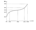
- FIG. 2 is a diagram showing a remaining capacity-voltage curve of the power storage unit 3.
- the horizontal axis indicates the remaining capacity (SOC: State of Charge) (%) of the power storage unit 3
- the vertical axis indicates the voltage (V) of the power storage unit 3.
- the SOC is a percentage (0 to 100%) of the current remaining capacity with respect to the full charge capacity.
- power storage unit 3 is 300 V when empty (SOC is 0%), 360 V when SOC is 20%, 380 V (rated voltage) when SOC is 50%, 400V when the SOC is 80%, and 420V when the SOC is fully charged (SOC is 100%).
- the voltage of the power storage unit 3 is suppressed to a fluctuation range of 380 ⁇ 20V.
- power storage unit 3 since the change in voltage is relatively stable with respect to the change in SOC, power storage unit 3 has a high voltage stabilization capability. Thereby, the power storage unit 3 can stably supply the power supply voltage to the DC bus 1.
- the power storage unit 3 is directly connected to the DC bus 1 and exchanges DC power with the DC bus 1.
- “directly connected” means that a power converter such as a DC / DC converter is not interposed between the DC bus 1 and the power storage unit 3. Therefore, the voltage of DC bus 1 is substantially equal to the power supply voltage of power storage unit 3.
- the grid power system 4 exchanges DC power with the DC bus 1.
- the grid power system 4 includes a DC / AC converter 50, an AC / DC converter 70, and a grid power 40.
- System power 40 is power received from an electric power company or the like (for example, AC 200V).
- the system power 40 is supplied from a single-phase three-wire commercial AC power system.
- the neutral wire is grounded via the resistor Rg1
- AC 200V is supplied using two wires other than the neutral wire (R-phase wire RL and T-phase wire TL). Supply.
- the DC / AC converter 50 and the AC / DC converter 70 are connected in parallel between the DC bus 1 and the system power 40.
- the DC / AC converter 50 converts the DC power received from the DC bus 1 into AC power and supplies it to the system power 40.
- the AC / DC converter 70 converts AC power received from the system power 40 into DC power and supplies it to the DC bus 1.
- system power is purchased from an electric power company or the like via the AC / DC converter 70 (power purchase), and surplus power is supplied from the electric power company or the like via the DC / AC converter 50. It is possible to sell to (power sale).
- FIG. 3 is a configuration diagram illustrating details of power storage unit 3 in FIG. 1.
- power storage unit 3 includes storage batteries 3-1, 3-2 and storage battery control units 4-1, 4-2.
- the first storage battery 3-1 and the second storage battery 3-2 are connected in series between the positive bus PL and the negative bus SL constituting the DC bus 1 via the storage battery control units 4-1 and 4-2. Part 3 is configured.
- Each of the first storage battery 3-1 and the second storage battery 3-2 includes a battery module in which a plurality of secondary battery cells are connected in series.
- the midpoint of storage battery control units 4-1, 4-2, that is, the midpoint of storage batteries 3-1, 3-2 (point B in the figure) is grounded through neutral point bus NL.
- a resistor Rg2 is inserted and connected to the neutral point bus NL.
- the line voltage between positive bus PL and negative bus SL is 380 V (rated voltage of power storage unit 3)
- the potentials at positive bus PL, negative bus SL, and midpoint B are +190 V, ⁇ 190 V, and ground, respectively. It becomes a potential (0 V).
- each of storage batteries 3-1 and 3-2 is composed of a secondary battery having a large capacity, so that each storage battery repeats charging / discharging, thereby causing positive bus PL and neutral point bus.
- Variations in the line voltage of NL and the line voltage between neutral point bus NL and negative bus SL can be leveled. Accordingly, these two line voltages can be kept in balance without performing complicated control, and a stable ground voltage can be generated at the middle point B of the power storage unit 3.
- the first storage battery control unit 4-1 monitors the state of the first storage battery 3-1, in order to protect the first storage battery 3-1, from overcharge, overdischarge, temperature rise, and the like. Specifically, the first storage battery control unit 4-1 includes the charge / discharge current input / output to / from the first storage battery 3-1, the charge / discharge voltage of the first storage battery 3-1 and the first storage battery 3-1. The temperature is detected, and the state (SOC and temperature state) of the first storage battery 3-1 is monitored based on the detected value. Further, the first storage battery control unit 4-1 transmits the state of the first storage battery 3-1 to the control device 60 of the DC / AC converter 50.
- the second storage battery control unit 4-2 monitors the state of the second storage battery 3-2. Specifically, the second storage battery control unit 4-2 performs charge / discharge current input / output to / from the second storage battery 3-2, charge / discharge voltage of the second storage battery 3-2, and the second storage battery 3-2. The temperature is detected, and the state (SOC and temperature state) of the second storage battery 3-2 is monitored based on the detected value. Further, the second storage battery control unit 4-2 transmits the state of the second storage battery 3-2 to the control device 60 of the DC / AC converter 50.
- FIG. 4 shows a more detailed configuration of the first storage battery 3-1 and the first storage battery control unit 4-1 in FIG.
- the configurations of the second storage battery 3-2 and the second storage battery control unit 4-2 are the same as the configurations of the first storage battery 3-1 and the first storage battery control unit 4-1, respectively.
- the configurations of the 3-1 and the first storage battery control unit 4-1 will be described.
- first storage battery 3-1 includes a plurality of battery cells 301 to 304 connected in series, and a plurality of cell measuring units 311 to 314 provided corresponding to each battery cell.
- four battery cells 301 to 304 are connected in series, but the number of battery cells is not particularly limited.
- Each cell measurement unit detects the “state value” of the corresponding battery cell. Specifically, each cell measurement unit detects the “state value” of the corresponding battery cell based on the output of the voltage sensor, current sensor, and temperature sensor (both not shown) provided in the corresponding battery cell. To do. That is, the “state value” includes the battery voltage, battery current, and battery temperature of the battery cell.
- the battery voltage, the battery current, and the battery temperature are collectively referred to as “battery data”.
- the battery data of the battery cells 301 to 304 detected by the cell measuring units 311 to 314 are output to the first battery control unit 4-1.
- the first battery control unit 4-1 includes a microcomputer 400, a voltage measurement unit 402, a current measurement unit 404, a cutoff unit 406, a communication unit 408, and an external IF (interface) 410.
- Voltage measuring unit 402 is provided between positive bus PL and neutral point bus NL. Voltage measurement unit 402 detects charge / discharge voltage Vb1 of first storage battery 3-1, and outputs the detected value to microcomputer 400.
- Current measuring unit 404 is connected to positive bus PL. Current measurement unit 404 detects charge / discharge current Ib1 of first storage battery 3-1, and outputs the detected value to microcomputer 400.
- FIG. 4 shows battery data (battery voltage, battery current and battery temperature of each battery cell) from the cell measuring units 311 to 314 inside the first storage battery 3-1, voltage measuring unit.
- the charge / discharge voltage Vb1 from 402 and the charge / discharge current Ib1 from the current measuring unit 404 are illustrated.
- the microcomputer 400 is configured to be able to communicate with a control device of the system power system 4 and the photovoltaic power generation system 2 and an external control device that performs overall control of the DC power supply system through the communication unit 408 and the external IF 410. Information from these control devices is also input to the microcomputer 400.
- the microcomputer 400 calculates the SOC (SOC1) of the first storage battery 3-1, based on the charge / discharge voltage Vb1 from the voltage measurement unit 402 and the charge / discharge current Ib1 from the current measurement unit 404. For example, the microcomputer 400 sequentially calculates the SOC1 of the first storage battery 3-1, based on the integrated value of the charge / discharge amount of the first storage battery 3-1.
- the integrated value of the charge / discharge amount can be obtained by temporally integrating the product (power) of the charge / discharge current and the charge / discharge voltage. Or you may calculate SOC1 based on the relationship between an open circuit voltage (OCV: Open Circuit Voltage) and SOC.
- the microcomputer 400 further calculates the degree of deterioration of the first storage battery 3-1 based on the battery data from the cell measuring units 311 to 314. As the degree of deterioration, internal resistance or full charge capacity can be used.
- the microcomputer 400 outputs the state value, SOC1, and degree of deterioration of the first storage battery 3-1 to an external control device through the communication unit 408 and the external IF 410.
- the microcomputer 400 monitors the state of the battery cells 301 to 304 based on the battery data from the cell measuring units 311 to 314.
- an abnormality such as overcharge, overdischarge, or overcurrent is detected in any of the battery cells 301 to 304
- an abnormality signal indicating an abnormality of the first storage battery 3-1 is detected through the communication unit 408 and the external IF 410. Is output to an external control device.
- blocking unit 406 that is inserted and connected to the DC bus 1 is provided.
- the blocking unit 406 is configured to be able to block the charging / discharging path of the first storage battery 3-1 in response to an abnormal signal from the microcomputer 400.
- blocking unit 406 includes a charge breaker that is inserted and connected to positive bus PL and that can block the charging path, and a discharge breaker that blocks the discharging path.
- the microcomputer 400 activates the abnormality signal and interrupts the charge / discharge path of the first storage battery 3-1 by the charge breaker and the discharge breaker.
- the microcomputer 400 conducts the discharge breaker that constitutes the cutoff unit 406 when the first storage battery 3-1 is discharged.
- the charging circuit breaker is cut off to keep the discharge path of the first storage battery 3-1 while blocking the charging path.
- the microcomputer 400 conducts the charging circuit breaker when charging the first storage battery 3-1, while the first storage battery 3--1.
- the discharge circuit breaker is interrupted by interrupting the discharge circuit breaker while maintaining the charging path of the first storage battery 3-1.
- the microcomputer 400 turns off the charging circuit breaker and the discharging circuit breaker to charge / discharge the first storage battery 3-1. Block the route.
- the second storage battery 3-2 is configured in the same manner as the first storage battery 3-1, and includes a plurality of battery cells connected in series and a plurality of cell measurement units provided corresponding to each battery cell.
- the battery data of each battery cell of the second storage battery 3-2 is output to the second storage battery control unit 4-2 (FIG. 3).
- the second storage battery control unit 4-2 includes a microcomputer, a voltage measurement unit, a current measurement unit, a cutoff unit, a communication unit, and an external IF.
- the voltage measuring unit detects the charge / discharge voltage Vb2 of the second storage battery 3-2 and outputs the detected value to the microcomputer.
- the current measuring unit detects the charging / discharging current Ib2 of the second storage battery 3-2 and outputs the detected value to the microcomputer.
- the microcomputer calculates the SOC (SOC2) of the second storage battery 3-2 based on the charge / discharge voltage Vb2 from the voltage measurement unit and the charge / discharge current Ib2 from the current measurement unit.
- the microcomputer calculates the degree of deterioration of the second storage battery 3-2 based on the battery data from the second storage battery control unit 4-2.
- the microcomputer outputs the state value, SOC2, and deterioration degree of the second storage battery 3-2 to the grid power system 4 through the communication unit and the external IF.
- the microcomputer monitors the state of the plurality of battery cells constituting the second storage battery 3-2 based on the battery data from the second storage battery control unit 4-2, and the microcomputer stores one of the plurality of battery cells.
- the charging / discharging path of the second storage battery 3-2 is blocked by controlling the blocking unit by the method described above.
- DC / AC converter 50 includes a DC / AC conversion unit 52, interconnection reactors 54 and 56, a DC voltage detection unit 58, and a control device 60.
- the DC / AC conversion unit 52 converts the DC power received from the DC bus 1 into AC power according to the switching control signals S1 to S4 from the control device 60, and outputs the AC power to the system power 40.
- the DC / AC converter 52 includes transistors Q1 to Q4, which are switching elements, and diodes D1 to D4. Transistors Q1 and Q3 are connected in series between positive bus PL and negative bus SL constituting DC bus 1. An intermediate point between transistors Q1 and Q3 is connected to R-phase line RL. Interconnection reactor 54 is connected to R-phase line RL.
- Transistors Q2 and Q4 are connected in series between positive bus PL and negative bus SL. An intermediate point between transistors Q2 and Q4 is connected to T-phase line TL. Interconnection reactor 56 is connected to T-phase line TL. Between the collector and emitter of each of the transistors Q1 to Q4, diodes D1 to D4 that flow current from the emitter side to the collector side are respectively connected.
- IGBTs Insulated Gate Bipolar Transistors
- MOSFET Metal Oxide Semiconductor Field-Effect Transistor
- the DC voltage detection unit 58 is connected between the positive bus PL and the negative bus SL, detects the voltage Vdc of DC power supplied from the DC bus 1 to the DC / AC converter 50, and the detection result is a control device. Output to 60.
- the control device 60 receives the voltage Vdc from the DC voltage detection unit 58, receives the battery information of the first storage battery 3-1, from the first storage battery control unit 4-1, and receives the second storage battery 3 from the second storage battery control unit 4-2. -2 battery information is received.
- the battery information of the first storage battery 3-1 includes the state value of the first storage battery 3-1 (charge / discharge voltage Vb 1, charge / discharge current Ib 1, battery temperature Tb 1), SOC 1, and the degree of deterioration.
- the battery information of the second storage battery 3-2 includes the state value of the second storage battery 3-2 (charge / discharge voltage Vb2, charge / discharge current Ib2, battery temperature Tb2), SOC2, and the degree of deterioration.
- control device 60 Based on the input information, control device 60 generates switching control signals S1 to S4 for controlling on / off of transistors Q1 to Q4 in accordance with a control structure to be described later, and controls DC / AC converter 52. To do.
- the control device 60 issues an abnormality signal indicating an abnormality of the first storage battery 3-1 or the second storage battery 3-2 from at least one of the first storage battery control unit 4-1 and the second storage battery control unit 4-2.
- the storage battery abnormality can be reflected in the control of the DC / AC converter 52.
- the control device 60 includes the transistor Q 1 that constitutes the DC / AC conversion unit 52. Switching control signals S1 to S4 are generated so that each of .about.Q4 stops the switching operation (all off).
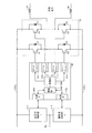
- FIG. 5 is a diagram showing a control structure of the control device 60 in FIG. Referring to FIG. 5, control device 60 includes a control unit 600, a communication unit 602, external IFs 604 and 606, and gate drivers 611 to 614.
- the controller 600 generates the switching control signals S1 to S4 so that the DC voltage Vdc becomes a predetermined voltage target value Vdc * during the power conversion operation.
- Voltage target value Vdc * can be determined in advance, such as 380 V, and stored in a storage unit (not shown). Alternatively, a desired voltage value may be appropriately acquired by performing communication with an external control device through the communication unit 602 and the external IF 604 or 606.
- the control unit 600 uses the transistors Q1 and Q4 as one set of switch pairs, the transistors Q2 and Q3 as another set of switch pairs, and alternately sets two sets of switch pairs. Turn on and off.
- the gate drivers 611 to 614 are provided corresponding to the control electrodes (gates or bases) of the transistors Q1 to Q4, respectively. Each of the gate drivers 611 to 614 drives and controls the control electrode of the corresponding transistor in accordance with a command from the control unit 600. Thereby, turn-on and turn-off of the two switch pairs are controlled.
- the battery information of the first storage battery 3-1 is input from the first storage battery control unit 4-1 to the control unit 600 through the external IF 604 and the communication unit 602. Further, the battery information of the second storage battery 3-2 is input to the control unit 600 from the second storage battery control unit 4-2 through the external IF 606 and the communication unit 602.
- control unit 600 When the control unit 600 receives the battery information of the first storage battery 3-1 and the second storage battery 3-2, there is an SOC imbalance (imbalance) between the first storage battery 3-1 and the second storage battery 3-2. Determine whether it has occurred. When it is determined that SOC imbalance occurs between first storage battery 3-1 and second storage battery 3-2, control unit 600 is generated based on voltage target value Vdc *. Correction processing for compensating the SOC imbalance between the first storage battery 3-1 and the second storage battery 3-2 is performed on the original switching control signals S 1 to S 4.
- control unit 600 uses transistors Q1 and Q4 constituting a full bridge circuit as one set of switch pairs and transistors Q2 and Q3 as another set of switch pairs. Turn on / off the switch pairs alternately. In FIG. 6, only the switch pair in the on state is represented by a solid line.
- control unit 600 turns off the switch pair of transistors Q2 and Q3, while switching the transistors Q1 and Q4.
- the pair is turned on / off at a predetermined duty ratio (the ratio of the on period to the switching period of the transistors Q1 to Q4).
- the current flows from the DC side to the AC side through the transistors Q1 and Q4 during the ON period of the transistors Q1 and Q4, thereby energizing from the DC side to the AC side.
- the electromagnetic energy in the current smoothing connected reactors 54 and 56 is returned to the DC side through the system power 40 and the diodes D2 and D3. If the electromagnetic energy in the current smoothing reactors 54 and 56 decreases during the off period of the transistors Q1 to Q4, the circuit is not energized.
- the control unit 600 turns off the switch pair of the transistors Q1 and Q4 while switching the switch pair of the transistors Q2 and Q3. Turn on / off at a predetermined duty ratio.
- this period 2 current flows from the DC side to the AC side through the transistors Q 2 and Q 3 during the ON period of the transistors Q 2 and Q 3, thereby energizing from the DC side to the AC side.
- the off period of the transistors Q1 to Q4 the electromagnetic energy in the current smoothing connected reactors 54 and 56 is returned to the DC side through the system power 40 and the diodes D1 and D4. If the electromagnetic energy in the current smoothing reactors 54 and 56 decreases during the off period of the transistors Q1 to Q4, the circuit is not energized.
- control unit 600 receives the battery information of the first storage battery 3-1 from the first storage battery control unit 4-1, and the second storage battery control unit 4-2. Based on the battery information of the second storage battery 3-2, it is determined whether or not there is an SOC imbalance between the first storage battery 3-1 and the second storage battery 3-2.
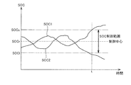
- control unit 600 sets the SOC control range of the first storage battery 3-1 and the second storage battery 3-2.
- the SOC control range is set so as to have control widths on the upper limit side and the lower limit side with respect to control center SOCr.
- the lower limit of the SOC control range is referred to as SOCl (control lower limit value)
- the upper limit of the SOC control range is referred to as SOCu (control upper limit value).
- Control unit 600 controls first storage battery 3-1 and first storage battery 3-1 so that SOC1 of first storage battery 3-1 and SOC2 of second storage battery 3-2 are maintained between control upper limit value SOCu and control lower limit value SOCl. 2 Controls charging / discharging of the storage battery 3-2.
- Control unit 600 determines that an SOC imbalance has occurred between first storage battery 3-1 and second storage battery 3-2. In this case, the control unit 600 uses the original switching control signals S1 to S4 generated based on the voltage target value Vdc * to change the SOC between the first storage battery 3-1 and the second storage battery 3-2. A correction process for compensating for imbalance is executed.
- FIG. 8 is a diagram for explaining the switching control for compensating for the SOC imbalance between the storage batteries 3-1 and 3-2.
- SOC imbalance compensation period for compensating for the SOC imbalance is provided between the periods.
- control unit 600 turns on / off transistors Q1 to Q4 so as to lower the SOC of storage battery 3-1 and 3-2 having the larger SOC to control center SOCr.
- the transistor Q1 is PWM-controlled as shown in FIG. Q4 is fixed off.
- the transistor Q1 to the interconnection reactor 54 to the R phase line RL to the neutral point A to the resistance Rg1 A current circulation path for discharging the first storage battery 3-1, that is, grounding, resistance Rg 2, and middle point B, is formed, and a discharge current flows through the current circulation path.
- FIG. 10 is a time waveform diagram for explaining the switching control shown in FIG.
- FIG. 10 shows time waveforms of the switching control signals S1 to S4 in the period 1 and the period 2 shown in FIG.
- switching control signals S1, S4 having a predetermined duty ratio are output from control unit 600.
- the switching control signals S1 and S4 are at the H (logic high) level
- the transistors Q1 and Q4 are both in the PWM control state.
- the switching control signals S2 and S3 are fixed at the L (logic low) level in the switching period (period of the carrier wave signal, period T in the figure).
- the control unit 600 calculates a deviation between the SOC 1 of the first storage battery 3-1 received from the first storage battery control unit 4-1, and the control center SOCr, and calculates an SOC imbalance compensation period according to the deviation.
- the switching control signals S1 and S4 are subjected to switching control when the SOC imbalance compensation period is ⁇ t.
- the signal S1 is corrected so as to be longer by ⁇ t.
- the transistor Q1 can be fixed on, while the transistor Q4 can be fixed off, and the current circulation path for discharging the first storage battery 3-1 shown in FIG. Can be formed.
- the control unit 600 outputs switching control signals S2 and S3 having a predetermined duty ratio and switching control signals S1 and S4 fixed at the L level in the switching period T.
- the control unit 600 corrects the switching control signals S2 and S3 so that the period during which the switching signal is at the H level is longer by the switching control signal S2 by ⁇ t.
- the switching control signals S1 and S4 in the period 1 are those of the switching control signal S4 during the period when the level is H level. Is corrected to be longer by ⁇ t.
- the switching control signals S2 and S3 are corrected so that the period during which the switching control signal S3 is at the H level is longer by ⁇ t in the switching control signal S3.
- the transistor Q4 or Q3 can be PWM-controlled, while the transistor Q1 or Q2 can be fixed off, and a current circulation path for discharging the second storage battery 3-2 is formed. can do.
- power storage unit 3 directly connected to DC bus 1 is configured with two storage batteries that are connected in series and whose midpoint is grounded.
- a stable ground voltage can be generated at the midpoint of the power storage unit by utilizing the high voltage stabilization capability of each storage battery.
- the first storage battery 3-1 or the second storage battery 3-2 is connected between the power storage unit 3 and the system power 40 via the DC / AC converter 50.
- a current circulation path for discharging can be formed.
- FIG. 11 is a diagram showing a control structure of the control unit 600 in FIG.
- control unit 600 includes subtraction unit 700, PI control unit 702, SOC correction unit 703, addition units 704 and 705, carrier wave comparators 706 to 709, NOT circuits 710 and 711, including.
- the subtraction unit 700 calculates a voltage deviation from the difference between the DC voltage Vdc and the voltage target value Vdc *, and outputs the voltage deviation to the PI control unit 702.
- the PI control unit 702 includes at least a proportional element (P: proportional element) and an integral element (I: integral element). Upon receiving a voltage deviation from the subtraction unit 700, the PI control unit 702 receives the voltage deviation according to the input voltage deviation.
- a duty ratio d is calculated as a ratio of the on period to the switching period (carrier wave signal period) of each of the transistors Q1 to Q4.
- the SOC correction unit 703 receives the SOC1 of the first storage battery 3-1 from the first storage battery control unit 4-1, and receives the SOC2 of the second storage battery 3-2 from the second storage battery control unit 4-2. Then, when the SOC correction unit 703 calculates the deviation between the larger one of SOC1 and SOC2 and the control center SOCr, the SOC correction unit 703 calculates the ON period of the transistor as the SOC imbalance compensation period according to the SOC deviation. Then, the SOC correction unit 703 calculates a correction amount ⁇ d of the duty ratio necessary to ensure the calculated on period.
- the addition unit 704 adds the duty ratio correction amount ⁇ d input from the SOC correction unit 703 to the duty ratio d input from the PI control unit 702 to generate a duty ratio command (d + ⁇ d). Adder 704 outputs the generated duty ratio command to carrier wave comparator 706.
- the addition unit 705 adds the duty ratio correction amount ⁇ d input from the SOC correction unit 703 to the duty ratio d input from the PI control unit 702 to generate a duty ratio command (d + ⁇ d).
- Adder 704 outputs the generated duty ratio command to carrier wave comparator 707.
- the carrier wave comparator 706 compares the duty ratio command (d + ⁇ d) with a carrier wave signal (for example, a triangular wave signal), inverts a binary signal corresponding to the comparison result by the NOT circuit 710, and turns on / off the transistor Q1.
- a switching control signal S1 for controlling OFF is generated.
- the carrier wave comparator 707 compares the duty ratio command (d + ⁇ d) with the carrier wave signal, and generates a switching control signal S2 for controlling on / off of the transistor Q2 composed of a binary signal according to the comparison result.
- the carrier wave comparator 708 compares the duty ratio command d and the carrier wave signal, and generates a switching control signal S3 for controlling on / off of the transistor Q3 composed of a binary signal according to the comparison result.
- the carrier wave comparator 709 compares the duty ratio command d and the carrier wave signal, inverts a binary signal corresponding to the comparison result by the NOT circuit 711, and controls a switching control signal for controlling on / off of the transistor Q4. S4 is generated.
- the transistor Q1 (or Q2) is controlled by controlling the switching control signal S1 (or S2) to be continuously at the H level even after the switching control signal S4 (or S3) transits to the L level.
- the SOC imbalance compensation period may be provided at any timing.
- the switching control signal S1 (or S2) may be shifted to the H level before the switching control signal S4 (or S3).
- a period in which only the switching control signal S1 (or S2) is at the H level may be provided at a timing different from the period in which the switching control signals S1, S4 (or S2, S3) are at the H level.
- the bipolar switching method has been described as the switching control of the power converter.
- the application of the present invention is not limited to the bipolar switching method.
- the present invention applies to all switching systems that are provided with an energy transmission period in which the transistors Q1 and Q4 or the transistors Q2 and Q3 are turned on and an SOC imbalance compensation period in which any one of the transistors Q1 to Q4 is turned on. It is possible to apply.
- the SOC of either one of the storage batteries 3-1 and 3-2 is When the control upper limit value SOCu is reached, or when one of the SOCs reaches the control lower limit value SOCl, it is determined that the SOC is unbalanced between the storage batteries, and the switching control signal is corrected. Also good.
- the middle point B is grounded by connecting the middle point B of the storage batteries 3-1 and 3-2 constituting the power storage unit 3 via the resistor Rg2.
- the DC / AC converter in which the neutral point A is electrically connected to the neutral point A of the single-phase three-wire AC power system is illustrated.
- the present invention can be applied to a DC / AC converter in which a neutral point A of an AC power system is electrically connected.
- the present invention is applicable to a configuration in which the middle point B of the power storage unit 3 is connected to a neutral line of a single-phase three-wire AC power system. In the configuration shown in FIG.
- a resistor Rg3 is inserted and connected to the neutral line connecting the middle point B of the power storage unit 3 and the neutral point A of the single-phase three-wire AC power system.
- the resistor Rg3 is connected to prevent an excessive current from flowing between the neutral point B and the neutral point A.
- the resistor Rg3 does not necessarily need to be connected to the neutral line.
- FIG. 13 is a circuit diagram showing a detailed configuration of the AC / DC converter 70 in FIG.
- AC / DC converter 70 has basically the same circuit configuration as DC / AC converter 50 shown in FIG. 3, and includes AC / DC converter 72, interconnection reactor 74, 76, a DC voltage detection unit 78, and a control device 80.
- AC / DC converter 72 converts AC power received from system power 40 into DC power and outputs it to DC bus 1 in accordance with switching control signals S11 to S14 from control device 80.
- AC / DC conversion unit 72 includes transistors Q11 to Q14, which are switching elements, and diodes D11 to D14.
- Transistors Q11 and Q13 are connected in series between positive bus PL and negative bus SL.
- An intermediate point between transistors Q11 and Q13 is connected to R-phase line RL.
- Interconnection reactor 74 is connected to R-phase line RL.
- Transistors Q12 and Q14 are connected in series between positive bus PL and negative bus SL. An intermediate point between transistors Q12 and Q14 is connected to T-phase line TL. Interconnection reactor 76 is inserted and connected to T-phase line TL. Between the collector and emitter of each of the transistors Q11 to Q14, diodes D11 to D14 that flow current from the emitter side to the collector side are respectively connected.
- IGBTs can be used as the transistors Q11 to Q14.
- a power switching element such as a power MOSFET may be used.
- DC voltage detector 78 is connected between positive bus PL and negative bus SL, detects voltage value Vdc of DC power supplied from AC / DC converter 72 to DC bus 1, and controls the detection result. Output to the device 80.
- the control device 80 receives the voltage Vdc from the DC voltage detection unit 78, receives battery information of the first storage battery 3-1, from the first storage battery control unit 4-1, and receives the second storage battery 3 from the second storage battery control unit 4-2. -2 battery information is received.
- the battery information of the first storage battery 3-1 includes the state value of the first storage battery 3-1 (charge / discharge voltage Vb 1, charge / discharge current Ib 1, battery temperature Tb 1), SOC 1, and the degree of deterioration.
- the battery information of the second storage battery 3-2 includes the state value of the second storage battery 3-2 (charge / discharge voltage Vb2, charge / discharge current Ib2, battery temperature Tb2), SOC2, and the degree of deterioration.
- control device 80 Based on the input information, control device 80 generates switching control signals S11 to S14 for controlling on / off of transistors Q11 to Q14 in accordance with a control structure described later, and controls AC / DC converter 72. To do.
- control device 80 generates switching control signals S11 to S14 so that DC voltage Vdc becomes predetermined voltage target value Vdc *.
- Voltage target value Vdc * can be determined in advance, such as 380 V, and stored in a storage unit (not shown). Or you may make it acquire a desired voltage value suitably by communicating between the control apparatus 80 and an external control apparatus.
- control device 80 turns off the switch pair of transistors Q11 and Q12, while turning on / off the switch pair of transistors Q13 and Q14 at a predetermined duty ratio.
- Period 1-1 electromagnetic current is accumulated in interconnection reactors 74 and 76 due to current flowing through transistors Q13 and Q14.
- the connection point between the diodes D11 and D13 and the connection point of the diodes D12 and D14 is between.
- the electromagnetic energy emitted from the interconnecting reactors 74 and 76 is received, and this electromagnetic energy is rectified to DC power.
- the transistors Q11 to Q14 are all turned off in the period 2 in which AC power is rectified to DC power by the diodes D11 and D14 constituting the bridge circuit. It is good also as composition which carries out synchronous rectification as an ON state.
- the control device 80 When the DC voltage Vdc is larger than the voltage target value Vdc *, the control device 80 reduces the duty ratio of the switch pair so as to reduce the energy transmitted to the DC side, that is, to shorten the period 1-1. Decrease. On the other hand, when the DC voltage Vdc is smaller than the voltage target value Vdc *, the control device 80 increases the duty of the switch pair so as to increase the energy transmitted to the DC side, that is, to lengthen the period 1-1. Increase the ratio.
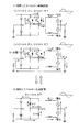
- FIG. 15 shows a state in which the power conversion operation is performed by a control mode different from FIG.
- control device 80 turns off the switch pair of transistors Q13 and Q14 and turns on and off the switch pair of transistors Q11 and Q12 in a half cycle of the system power.
- period 1-2 In the on period of transistors Q11 and Q12 (hereinafter referred to as “period 1-2”), current flows through transistors Q11 and Q12, and electromagnetic energy is accumulated in interconnection reactors 74 and 76.
- the interconnection reactor 74 between the connection point of the diodes D11 and D13 and the connection point of the diodes D12 and D14, the electromagnetic energy emitted from 76 is received, and this electromagnetic energy is rectified into DC power.
- the control device 80 When the DC voltage Vdc is larger than the voltage target value Vdc *, the control device 80 reduces the duty ratio of the switch pair so as to reduce the energy transmitted to the DC side, that is, to shorten the period 1-2. Decrease. On the other hand, when the DC voltage Vdc is smaller than the voltage target value Vdc *, the control device 80 increases the duty of the switch pair so as to increase the energy transmitted to the DC side, that is, to lengthen the period 1-2. Increase the ratio.
- the second storage battery 3-2 is discharged in the on-period (period 1-1) of the transistors Q13 and Q14, while FIG.
- first storage battery 3-1 is discharged during the on period (period 1-2) of transistors Q11 and Q12.
- the AC / DC converter 70 as the correction process for compensating for the SOC imbalance between the storage batteries 3-1, 3-2, the SOC1 and the second of the first storage battery 3-1.
- the control mode of FIG. 14 and the control mode of FIG. 15 are switched and executed in accordance with the SOC2 deviation of the storage battery 3-2.
- FIG. 16 is a diagram for explaining switching control for compensating for SOC imbalance between the storage batteries 3-1 and 3-2.
- control device 80 compares SOC1 of first storage battery 3-1 with SOC2 of second storage battery 3-2, and the comparison result is obtained. Accordingly, one of the switching control shown in FIG. 5A and the switching control shown in FIG.
- the first storage battery 3-1 or the second storage battery is connected between the power storage unit 3 and the system power 40 via the AC / DC converter 70.
- a current circulation path for discharging 3-2 can be formed.
- one of the first storage battery 3-1 and the second storage battery 3-2 can be prevented from being overdischarged or overcharged, and a state where only one of the storage batteries is charged / discharged can be avoided. It is possible to prevent the power storage unit 3 from progressing.
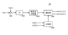
- FIG. 17 is a diagram showing a control structure of the control device 80 in FIG. Referring to FIG. 17, control device 80 includes a subtraction unit 800, a PI control unit 802, a carrier wave comparator 804, a selection unit 806, and a comparison unit 808.
- the subtraction unit 800 calculates a voltage deviation from the difference between the DC voltage Vdc and the voltage target value Vdc *, and outputs the voltage deviation to the PI control unit 802.
- the PI control unit 802 includes at least a proportional element P and an integration element I.
- the PI control unit 802 changes the switching period (carrier wave) of each of the transistors Q11 to Q14 according to the input voltage deviation.
- the duty ratio d as a ratio of the ON period to the signal period) is calculated.
- the carrier wave comparator 804 compares the duty ratio d with a carrier wave signal (for example, a triangular wave signal), and performs switching control for controlling on / off of the transistors Q11 to Q14 composed of binary signals according to the comparison result. Signals S11 to S14 are generated. Specifically, carrier wave comparator 804 uses switching control signals S11 and S12 for controlling on / off of the switch pair of transistors Q11 and Q12 as one set of switching control signals, and sets the switch pair of transistors Q13 and Q14. Two sets of switching control signals (S11, S12) and (S13, S14) are generated using the switching control signals S13 and S14 as another set of switching control signals in order to control on / off.
- a carrier wave signal for example, a triangular wave signal
- the comparison unit 808 compares the SOC1 of the first storage battery 3-1 received from the first storage battery control unit 4-1, and the SOC2 of the second storage battery 3-2 received from the second storage battery control unit 4-2. Then, the comparison unit 808 outputs a signal indicating the comparison result to the selection unit 806.
- the selection unit 806 selects one of the two sets of switching control signals (S11, S12) and (S13, S14) based on the comparison result signal received from the comparison unit 808. Specifically, when it is determined from the comparison result signal that the SOC2 of the second storage battery 3-2 is larger than the SOC1 of the first storage battery 3-1, the selection unit 806 selects the switching control signal (S13, S14). Select. In this case, the selection unit 806 fixes the non-selected switching control signals (S11, S12) to the L level.
- the selection unit 806 selects the switching control signal (S11, S12). . In this case, the selection unit 806 fixes the non-selected switching control signals (S13, S14) to the L level.
- the AC / DC converter according to the present embodiment provides the SOC imbalance compensation period by the control method as shown in FIG. 15, but provides a period during which any one of the transistors Q11 to Q14 is turned on.
- the SOC imbalance between the storage batteries 3-1 and 3-2 may be corrected.
- the middle point B is grounded by connecting the middle point B of the storage batteries 3-1 and 3-2 constituting the power storage unit 3 via the resistor Rg2.
- an AC / DC converter in which a neutral point A of a single-phase three-wire AC power system is electrically connected is illustrated.
- the present invention relates to a middle point B of the power storage unit 3 and a single-phase three-wire system.
- the present invention can be applied to an AC / DC converter in which a neutral point A of an AC power system is electrically connected.
- the present invention can also be applied to a configuration in which the middle point B of the power storage unit 3 is connected to a neutral line of a single-phase three-wire AC power system.
- the power storage unit directly connected to the DC bus is configured by two storage batteries that are connected in series and whose midpoint is grounded. This makes it possible to generate a stable ground voltage at the midpoint by utilizing the energy leveling capability of each storage battery.
- the power conversion device by performing switching control to compensate for the SOC imbalance between the two storage batteries connected in series, it is possible to suppress variation in performance between the storage batteries, Progress of deterioration of the power storage unit can be suppressed.
- the present invention can be used for a DC power supply system in which a power storage unit is directly connected to a DC bus without using a power converter.
Landscapes
- Engineering & Computer Science (AREA)
- Power Engineering (AREA)
- Charge And Discharge Circuits For Batteries Or The Like (AREA)
- Supply And Distribution Of Alternating Current (AREA)
- Direct Current Feeding And Distribution (AREA)
- Inverter Devices (AREA)
Abstract
直流給電システムは、単相3線式の電力系統および直流負荷(5)の間に配設された直流バス(1)と、電源電圧を直流バス(1)に出力する蓄電部(3)と、直流バス(1)と電力系統との間で電力変換を行なう電力変換装置(50,70)とを備える。蓄電部(3)は、直流バス(1)の直流正負母線間に直列に接続され、かつ、その中点が接地された2個の蓄電池(3-1,3-2)を含む。電力変換装置(50,70)は、直流バス(1)の直流電圧および蓄電池(3-1,3-2)の各々の残容量に基づいて電力変換を制御するための制御装置(60,80)を含む。
Description
この発明は、直流給電システムに関し、より特定的には、蓄電部が電力変換器を介さず直流バスに直結された直流給電システムに関する。
近年、太陽電池、風力発電装置および燃料電池のような分散電源装置が普及し始めている。現状では、分散電源装置が発電した直流電力を交流電力に変換し、さらに、その交流電力を、電力を消費する機器において直流電力に変換して使用する。このように、直流-交流変換および交流-直流変換が行なわれるため、その電力変換のたびに電力損失が生じる。そこで、分散電源装置が発電する直流電力を交流電力に変換することなく、直流電力のまま送電して機器で使用することにより、変換損失を低減させる直流給電システムが提案されている。
このような直流給電システムにおいては、単相3線式の商用電力系統に連系される電力変換装置によって、分散電源装置が発電する直流電力を交流電力に変換して商用電力系統に供給するとともに、商用電力系統の交流電力を直流電力に変換して機器に供給する構成が採用されている。そして、この種の電力変換装置としては、複数のスイッチング素子からなるインバータブリッジと連系リレーとから構成され、インバータブリッジでPWM(パルス幅変調)制御によって直流電力を交流電力に変換して、連系リレーを介して単相3線式の商用電力系統の中性線以外の2線(R相線、T相線)に供給可能に構成されたものがある。
上記の従来の電力変換装置においては、インバータブリッジの直流側には、インバータブリッジへの入力電圧の変動を抑えるために、直列接続された2個のコンデンサからなる平滑回路が接続されている。そして、この2個のコンデンサの中点は、単相3線式の商用電力系統の中性点に接続されている。2個のコンデンサの中点と単相3線式の商用電力系統の中性点とを接続することによって、R相線および中性線間および中性線およびT相線間に対して同じ電圧を供給するためである。
しかしながら、インバータブリッジの特性の変化やPWM制御における制御誤差などの要因により、2個のコンデンサが必ずしも同じ電圧を出力するとは限らず、2個のコンデンサの間で電圧のアンバランスが生じるという不具合が起きてしまう。そして、2個のコンデンサの間で電圧のアンバランスが生じると、2個のコンデンサの中点の対地電圧が不安定となる虞がある。
それゆえ、この発明はかかる課題を解決するためになされたものであり、その目的は、蓄電部が電力変換器を介さず直流バスに直結された直流給電システムにおいて、直流バスの対地電圧を安定化することである。
この発明のある局面に従えば、直流負荷に直流電力を供給するための直流給電システムであって、系統電力および直流負荷の間に配設された直流正負母線と、電源電圧を直流正負母線に出力する蓄電部と、直流正負母線と電力系統との間で電力変換を行なう電力変換装置とを備える。蓄電部は、直流正負母線間に直列に接続され、かつ、その中点が接地された第1および第2の蓄電池を含む。
好ましくは、系統電力は、単相3線式の電力系統を含む。蓄電部は、第1および第2の蓄電池の各々の状態値に基づいて、第1および第2の蓄電池の各々の残容量を検出するための残容量検出部をさらに含む。電力変換装置は、直流正負母線に接続され、複数のスイッチング素子によって蓄電部の直流電力および電力系統の交流電力の間で電力変換を行なう電力変換回路と、直流正負母線間の直流電圧および残容量検出部の検出値に基づいて、複数のスイッチング素子をスイッチング制御するための電力変換制御部とを含む。
好ましくは、電力変換制御部は、直流電圧目標値と直流正負母線間の直流電圧との偏差に基づいて、複数のスイッチング素子をスイッチング制御するための第1のスイッチング制御部と、第1の蓄電池の残容量検出値と第2の蓄電池の残容量検出値との偏差に基づいて、複数のスイッチング素子をスイッチング制御するための第2のスイッチング制御部とを含む。
好ましくは、第2のスイッチング制御部は、第1の蓄電池および第2の蓄電池のうちの一方の残容量検出値が制御範囲の上限値に達するという第1の条件、第1の蓄電池および第2の蓄電池のうちの他方の残容量検出値が制御範囲の下限値に達するという第2の条件の少なくとも一方が成立すると、残容量検出値の偏差に基づいて複数のスイッチング素子をスイッチング制御する。
好ましくは、第2のスイッチング制御部は、第1の蓄電池の残容量検出値が第2の蓄電池の残容量検出値よりも大きい場合には、蓄電部および電力系統の間で、第1の蓄電池を放電するための電流循環経路が形成されるように、複数のスイッチング素子をスイッチング制御する。
好ましくは、第2のスイッチング制御部は、第2の蓄電池の残容量検出値が第1の蓄電池の残容量検出値よりも大きい場合には、蓄電部および電力系統の間で、第2の蓄電池を放電するための電流循環経路が形成されるように、複数のスイッチング素子をスイッチング制御する。
好ましくは、蓄電部は、第1および第2の蓄電池の少なくとも一方に異常が検知された場合には、当該異常が検知された蓄電池の充放電経路を遮断するための遮断部をさらに含む。
好ましくは、直流給電システムは、蓄電部の中点および電力系統の中性点を接続する配線をさらに備える。
この発明によれば、直流バスに電力変換器を介さず蓄電部を直結した直流給電システムにおいて、該蓄電部を、直流正負母線間に直列接続され、かつその中点を接地した2個の蓄電池により構成することにより、各蓄電池が有するエネルギー平準化能力を活かして、蓄電部の中点に安定した対地電圧を生成することができる。
また、当該2個の蓄電池の残容量の偏差に応じて電力変換回路のスイッチング制御を行なうことにより蓄電池間の残容量の不均衡を抑制することができる。この結果、蓄電部の劣化の進行を抑制することができる。
以下、本発明の実施の形態について、図面を参照しながら詳細に説明する。なお、図中の同一または相当する部分には同一符号を付してその説明は繰返さない。
(直流給電システムの構成)
図1は、この発明の実施の形態に従う直流給電システムの全体の構成を概略的に示す図である。
図1は、この発明の実施の形態に従う直流給電システムの全体の構成を概略的に示す図である。
図1を参照して、本実施の形態に従う直流給電システムは、直流バス1と、太陽光発電システム2と、蓄電部3と、系統電力システム4とを備える。
直流バス1は、直流負荷群5に直流電力を供給する。直流負荷群5は、一例として、家庭で使用される空調機、冷蔵庫、洗濯機、テレビ、照明装置またはパーソナルコンピュータのような電気機器である。あるいは、オフィスで使用されるコンピュータ、複写機またはファクシミリのような電気機器や、または、店舗で使用されるショーケースまたは照明装置のような電気機器であってもよい。直流バス1には、太陽光発電システム2、蓄電部3および系統電力システム4が接続されている。
なお、本実施の形態に従う直流給電システムにおいては、直流バス1、太陽光発電システム2、蓄電部3、系統電力システム4および直流負荷群5をそれぞれ1個ずつ備える場合について説明するが、これらの個数には制限がなく、1個でも複数個であってもよい。
直流バス1は、電力線対である正母線PLおよび負母線SLで構成される。
太陽光発電システム2は、太陽電池20と、DC/DC変換器30とを含む。DC/DC変換器30は、太陽電池20と直流バス1との間に配置されており、太陽電池20から受ける直流電力を電圧変換して直流バス1へ供給する。DC/DC変換器30における電圧変換動作は、太陽電池20の出力電圧と、直流バス1の電圧(正母線PLおよび負母線SLの間の線間電圧)とに応じて、図示しない制御部からのスイッチング指令に従って制御される。
太陽光発電システム2は、太陽電池20と、DC/DC変換器30とを含む。DC/DC変換器30は、太陽電池20と直流バス1との間に配置されており、太陽電池20から受ける直流電力を電圧変換して直流バス1へ供給する。DC/DC変換器30における電圧変換動作は、太陽電池20の出力電圧と、直流バス1の電圧(正母線PLおよび負母線SLの間の線間電圧)とに応じて、図示しない制御部からのスイッチング指令に従って制御される。
蓄電部3は、再充電可能な電力貯蔵要素であり、代表的にリチウムイオン二次電池やニッケル水素電池などの二次電池で構成される。蓄電部3は、複数の二次電池セルからなる蓄電池を2組直列に接続し、両蓄電池の中点と接地との間に抵抗Rg2を接続した構成とする。蓄電部3は、一例として、定格電圧380Vおよび蓄電池容量10Ahを有している。
図2は、蓄電部3の残容量-電圧曲線を示す図である。図2において、横軸は蓄電部3の残容量(SOC:State of Charge)(%)、縦軸は蓄電部3の電圧(V)を示している。なお、SOCは、満充電容量に対する現在の残容量を百分率(0~100%)で示したものである。図2を参照して、蓄電部3は、空状態(SOCが0%)のときに300Vとなり、SOCが20%のときに360Vとなり、SOCが50%のときに380V(定格電圧)となり、SOCが80%のときに400Vとなり、満充電状態(SOCが100%)のときに420Vとなる。
図2に示す特性において、20%から80%までの広いSOCの範囲で、蓄電部3の電圧は380±20Vの変動範囲に抑えられている。このように、SOCの変化に対して電圧の変化が比較的安定しているため、蓄電部3は高い電圧安定化能力を有している。これにより、蓄電部3は、直流バス1に電源電圧を安定して供給することができる。
図1に示す構成において、蓄電部3は、直流バス1に直結されており、直流バス1との間で直流電力の授受を行なう。ここで、「直結」とは、直流バス1と蓄電部3との間に、DC/DC変換器のような電力変換器が介在していないことを意味する。したがって、直流バス1の電圧は、蓄電部3の電源電圧とほぼ等しくなる。このように蓄電部3を直流バス1に直結する構成としたことにより、蓄電部3が有する高い電圧安定化能力を活かして、急激な負荷変動による直流バス1の電圧変動を抑制することが可能となる。
系統電力システム4は、直流バス1との間で直流電力の授受を行なう。系統電力システム4は、DC/AC変換器50と、AC/DC変換器70と、系統電力40とを含む。
系統電力40は、電力会社等から受電する電力(たとえば、AC200Vとする)である。系統電力40は、単相3線式の商用交流電力系統から供給される。単相3線式の商用交流電力系統は、中性線が抵抗Rg1を介して接地されており、中性線以外の2線(R相線RLおよびT相線TL)を使用してAC200Vを供給する。
DC/AC変換器50およびAC/DC変換器70は、直流バス1および系統電力40の間に並列接続される。DC/AC変換器50は、直流バス1から受ける直流電力を交流電力に変換して系統電力40へ供給する。一方、AC/DC変換器70は、系統電力40から受ける交流電力を直流電力に変換して直流バス1へ供給する。本実施の形態に従う直流給電システムにおいては、AC/DC変換器70を介して電力会社等から系統電力を買う(買電)するとともに、DC/AC変換器50を介して余剰電力を電力会社等に売る(売電)することを可能に構成されている。
(蓄電部の構成)
次に、図面を参照して、この発明の実施の形態に従う直流給電システムに適用される蓄電部3の構成について説明する。
次に、図面を参照して、この発明の実施の形態に従う直流給電システムに適用される蓄電部3の構成について説明する。
図3は、図1における蓄電部3の詳細を説明する構成図である。
図3を参照して、蓄電部3は、蓄電池3-1,3-2と、蓄電池制御部4-1,4-2とを含む。
図3を参照して、蓄電部3は、蓄電池3-1,3-2と、蓄電池制御部4-1,4-2とを含む。
第1蓄電池3-1および第2蓄電池3-2は、蓄電池制御部4-1,4-2を介して直流バス1を構成する正母線PLおよび負母線SLの間に直列に接続され、蓄電部3を構成する。第1蓄電池3-1および第2蓄電池3-2の各々は、複数の二次電池セルが直列接続されてなる電池モジュールから構成される。蓄電池制御部4-1,4-2の中点、すなわち、蓄電池3-1,3-2の中点(図中の点B)は、中性点母線NLを介して接地される。中性点母線NLには、抵抗Rg2が介挿接続されている。したがって、たとえば正母線PLおよび負母線SLの線間電圧が380V(蓄電部3の定格電圧)である場合、正母線PL、負母線SL、中点Bにおける電位はそれぞれ、+190V,-190V,接地電位(0V)となる。
なお、図3に示すように、蓄電池3-1,3-2の各々を大容量の二次電池により構成したことによって、各蓄電池が充放電を繰り返すことによって、正母線PLおよび中性点母線NLの線間電圧、および中性点母線NLおよび負母線SL間の線間電圧の変動を平準化することができる。これにより、複雑な制御を行なうことなく、これら2つの線間電圧を平衡に保つことができ、蓄電部3の中点Bに安定した対地電圧を生成することができる。
第1蓄電池制御部4-1は、過充電、過放電および温度上昇などから第1蓄電池3-1を保護するために、第1蓄電池3-1の状態を監視する。具体的には、第1蓄電池制御部4-1は、第1蓄電池3-1に対して入出力される充放電電流、第1蓄電池3-1の充放電電圧および第1蓄電池3-1の温度を検出し、その検出値に基づいて第1蓄電池3-1の状態(SOCおよび温度状態)を監視する。また、第1蓄電池制御部4-1は、第1蓄電池3-1の状態をDC/AC変換器50の制御装置60へ送信する。
第2蓄電池制御部4-2は、第2蓄電池3-2の状態を監視する。具体的には、第2蓄電池制御部4-2は、第2蓄電池3-2に対して入出力される充放電電流、第2蓄電池3-2の充放電電圧および第2蓄電池3-2の温度を検出し、その検出値に基づいて第2蓄電池3-2の状態(SOCおよび温度状態)を監視する。また、第2蓄電池制御部4-2は、第2蓄電池3-2の状態をDC/AC変換器50の制御装置60へ送信する。
図4には、図3における第1蓄電池3-1および第1蓄電池制御部4-1のさらに詳細な構成が示される。なお、第2蓄電池3-2および第2蓄電池制御部4-2の構成は、第1蓄電池3-1および第1蓄電池制御部4-1の構成とそれぞれ同様であるので、以下では第1蓄電池3-1および第1蓄電池制御部4-1の構成について説明する。
図4を参照して、第1蓄電池3-1は、直列接続された複数の電池セル301~304と、各電池セルに対応して設けられた複数のセル測定部311~314とを含む。なお、図4では、4個の電池セル301~304を直列接続させているが、電池セルの個数は特に限定されるものではない。
各セル測定部は、対応する電池セルの「状態値」を検出する。具体的には、各セル測定部は、対応する電池セルに設けられた電圧センサ、電流センサおよび温度センサ(ともに図示せず)の出力に基づいて、対応する電池セルの「状態値」を検出する。すなわち、「状態値」は、電池セルの電池電圧、電池電流および電池温度を含む。以下では、電池電圧、電池電流および電池温度を包括的に「電池データ」とも総称する。セル測定部311~314によりそれぞれ検出された電池セル301~304の電池データは、第1電池制御部4-1へ出力される。
第1電池制御部4-1は、マイコン400と、電圧測定部402と、電流測定部404と、遮断部406と、通信部408と、外部IF(インターフェース)410とを含む。
電圧測定部402は、正母線PLおよび中性点母線NLの間に設けられる。電圧測定部402は、第1蓄電池3-1の充放電電圧Vb1を検出し、その検出値をマイコン400へ出力する。電流測定部404は、正母線PLに介挿接続される。電流測定部404は、第1蓄電池3-1の充放電電流Ib1を検出し、その検出値をマイコン400へ出力する。
マイコン400に入力される情報として、図4には、第1蓄電池3-1内部のセル測定部311~314からの電池データ(各電池セルの電池電圧、電池電流および電池温度)、電圧測定部402からの充放電電圧Vb1および電流測定部404からの充放電電流Ib1を例示する。図示しないが、マイコン400は、通信部408および外部IF410を通じて、系統電力システム4および太陽光発電システム2の制御装置や直流給電システムを統括制御する外部の制御装置と通信可能に構成されており、これらの制御装置からの情報についても、マイコン400に入力される。
マイコン400は、電圧測定部402からの充放電電圧Vb1および電流測定部404からの充放電電流Ib1に基づいて、第1蓄電池3-1のSOC(SOC1)を演算する。たとえば、マイコン400は、第1蓄電池3-1の充放電量の積算値に基づいて第1蓄電池3-1のSOC1を順次演算する。充放電量の積算値は、充放電電流および充放電電圧の積(電力)を時間的に積分することで得られる。あるいは、開放電圧(OCV:Open Circuit Voltage)とSOCとの関係に基づいてSOC1を算出してもよい。マイコン400は、さらに、セル測定部311~314からの電池データに基づいて、第1蓄電池3-1の劣化度合いを演算する。劣化度合いとしては、内部抵抗や満充電容量を用いることができる。マイコン400は、第1蓄電池3-1の状態値、SOC1および劣化度合いを、通信部408および外部IF410を通じて、外部の制御装置へ出力する。
また、マイコン400は、セル測定部311~314からの電池データに基づいて、電池セル301~304の状態を監視する。そして、電池セル301~304のいずれかに過充電、過放電や過電流などの異常が検知された場合には、通信部408および外部IF410を通じて、第1蓄電池3-1の異常を示す異常信号を外部の制御装置へ出力する。
第1蓄電池3-1および系統電力システム4の間には、直流バス1に介挿接続された遮断部406が設けられる。この遮断部406は、マイコン400からの異常信号に応答して第1蓄電池3-1の充放電経路を遮断可能に構成される。たとえば、遮断部406は、正母線PLに介挿接続された、充電経路を遮断可能にする充電遮断器と放電経路を遮断する放電遮断器とで構成される。第1蓄電池3-1の異常が検知されると、マイコン400は、異常信号を活性化し、充電遮断器および放電遮断器により第1蓄電池3-1の充放電経路を遮断する。
具体的には、第1蓄電池3-1の過充電または過電流が検知された場合には、マイコン400は、第1蓄電池3-1の放電時には遮断部406を構成する放電用遮断器を導通する一方で、第1蓄電池3-1の充電時には充電用遮断器を遮断することにより第1蓄電池3-1の放電経路を保ちつつ充電経路を遮断する。これに対して、第1蓄電池3-1の過放電が検知された場合には、マイコン400は、第1蓄電池3-1の充電時には充電用遮断器を導通する一方で、第1蓄電池3-1の放電時には放電用遮断器を遮断することにより第1蓄電池3-1の充電経路を保ちつつ放電経路を遮断する。さらに、第1蓄電池3-1が高温となる異常温度が検知された場合には、マイコン400は、充電用遮断器および放電用遮断器を遮断することにより、第1蓄電池3-1の充放電経路を遮断する。
第2蓄電池3-2は、第1蓄電池3-1と同様に構成され、直列接続された複数の電池セルと、各電池セルに対応して設けられた複数のセル測定部とを含む。第2蓄電池3-2の各電池セルの電池データは、第2蓄電池制御部4-2(図3)へ出力される。
第2蓄電池制御部4-2は、第1蓄電池制御部4-1と同様に、マイコン、電圧測定部、電流測定部、遮断部、通信部および外部IFを含んで構成される。電圧測定部は、第2蓄電池3-2の充放電電圧Vb2を検出し、その検出値をマイコンへ出力する。電流測定部は、第2蓄電池3-2の充放電電流Ib2を検出し、その検出値をマイコンへ出力する。マイコンは、電圧測定部からの充放電電圧Vb2および電流測定部からの充放電電流Ib2に基づいて、第2蓄電池3-2のSOC(SOC2)を演算する。また、マイコンは、第2蓄電池制御部4-2からの電池データに基づいて、第2蓄電池3-2の劣化度合いを演算する。マイコンは、第2蓄電池3-2の状態値、SOC2および劣化度合いを、通信部および外部IFを通じて、系統電力システム4へ出力する。
さらに、マイコンは、第2蓄電池制御部4-2からの電池データに基づいて、第2蓄電池3-2を構成する複数の電池セルの状態を監視しており、複数の電池セルのいずれかに異常が検知された場合には、上述した方法によって遮断部を制御することにより、第2蓄電池3-2の充放電経路を遮断する。
(DC/AC変換器の構成)
再び図3を参照して、この発明の実施の形態に従う直流給電システムに適用される電力変換装置の一形態であるDC/AC変換器50の構成について説明する。
再び図3を参照して、この発明の実施の形態に従う直流給電システムに適用される電力変換装置の一形態であるDC/AC変換器50の構成について説明する。
図3を参照して、DC/AC変換器50は、DC/AC変換部52と、連系リアクトル54,56と、直流電圧検出部58と、制御装置60とを含む。
DC/AC変換部52は、制御装置60からのスイッチング制御信号S1~S4に応じて、直流バス1から受けた直流電力を交流電力に変換して系統電力40へ出力する。DC/AC変換部52は、スイッチング素子であるトランジスタQ1~Q4と、ダイオードD1~D4とを含む。トランジスタQ1,Q3は、直流バス1を構成する正母線PLおよび負母線SLの間に直列に接続される。トランジスタQ1とトランジスタQ3との中間点はR相線RLに接続される。連系リアクトル54は、R相線RLに介挿接続される。
トランジスタQ2,Q4は、正母線PLおよび負母線SLの間に直列に接続される。トランジスタQ2とトランジスタQ4との中間点はT相線TLに接続される。連系リアクトル56は、T相線TLに介挿接続される。各トランジスタQ1~Q4のコレクタ-エミッタ間には、エミッタ側からコレクタ側へ電流を流すダイオードD1~D4がそれぞれ接続されている。
なお、トランジスタQ1~Q4として、たとえば、IGBT(Insulated Gate Bipolar Transistor)を用いることができる。または、パワーMOSFET(Metal Oxide Semiconductor Field-Effect Transistor)等の電力スイッチング素子を用いてもよい。
直流電圧検出部58は、正母線PLと負母線SLとの間に接続され、直流バス1からDC/AC変換器50へ供給される直流電力の電圧Vdcを検出し、その検出結果を制御装置60へ出力する。
制御装置60は、直流電圧検出部58から電圧Vdcを受け、第1蓄電池制御部4-1から第1蓄電池3-1の電池情報を受け、第2蓄電池制御部4-2から第2蓄電池3-2の電池情報を受ける。第1蓄電池3-1の電池情報には、第1蓄電池3-1の状態値(充放電電圧Vb1,充放電電流Ib1,電池温度Tb1)、SOC1および劣化度合いなどが含まれる。第2蓄電池3-2の電池情報には、第2蓄電池3-2の状態値(充放電電圧Vb2,充放電電流Ib2,電池温度Tb2)、SOC2および劣化度合いなどが含まれる。制御装置60は、これらの入力情報に基づいて、後述する制御構造に従って、トランジスタQ1~Q4のオン・オフを制御するためのスイッチング制御信号S1~S4を生成し、DC/AC変換部52を制御する。
また、制御装置60は、第1蓄電池制御部4-1および第2蓄電池制御部4-2の少なくとも一方から、第1蓄電池3-1または第2蓄電池3-2の異常を示す異常信号が発せられた場合には、蓄電池の異常をDC/AC変換部52の制御に反映することが可能に構成されている。具体的には、第1蓄電池3-1および第2蓄電池3-2の少なくとも一方の充放電経路が遮断されている場合には、制御装置60は、DC/AC変換部52を構成するトランジスタQ1~Q4の各々がスイッチング動作を停止(すべてオフ)するように、スイッチング制御信号S1~S4を生成する。
図5は、図3における制御装置60の制御構造を示す図である。
図5を参照して、制御装置60は、制御部600と、通信部602と、外部IF604,606と、ゲートドライバ611~614とを含む。
図5を参照して、制御装置60は、制御部600と、通信部602と、外部IF604,606と、ゲートドライバ611~614とを含む。
制御部600は、電力変換動作時には、直流電圧Vdcが所定の電圧目標値Vdc*となるようにスイッチング制御信号S1~S4を生成する。なお、電圧目標値Vdc*は、たとえば380Vのように事前に決定し、図示しない記憶部に格納しておくことができる。あるいは、通信部602および外部IF604または606を通じて、外部の制御装置との間で通信を行なうことによって、所望の電圧値を適宜取得するようにしてもよい。
制御部600は、フルブリッジ回路を構成するトランジスタQ1~Q4において、トランジスタQ1およびQ4を1組のスイッチペアとし、トランジスタQ2およびQ3をもう1組のスイッチペアとして、2組のスイッチペアを交互にオン・オフさせる。
ゲートドライバ611~614は、トランジスタQ1~Q4の制御電極(ゲートまたはベース)に対応してそれぞれ設けられる。ゲートドライバ611~614の各々は、制御部600からの指令に従って、対応するトランジスタの制御電極を駆動制御する。これにより、2組のスイッチペアのターンオンおよびターンオフが制御される。
図5に示す構成において、制御部600には、外部IF604および通信部602を通じて、第1蓄電池制御部4-1から第1蓄電池3-1の電池情報が入力される。また、制御部600には、外部IF606および通信部602を通じて、第2蓄電池制御部4-2から第2蓄電池3-2の電池情報が入力される。
制御部600は、第1蓄電池3-1および第2蓄電池3-2の電池情報を受けると、第1蓄電池3-1および第2蓄電池3-2の間でSOCのアンバランス(不均衡)が生じているか否かを判断する。そして、第1蓄電池3-1および第2蓄電池3-2の間でSOCのアンバランスが生じていると判断された場合には、制御部600は、電圧目標値Vdc*に基づいて生成された本来のスイッチング制御信号S1~S4に対して、第1蓄電池3-1および第2蓄電池3-2間のSOCのアンバランスを補償するための補正処理を実行する。
以下、図6を参照して、DC/AC変換器50の電力変換動作について説明する。
電力変換動作時においては、制御部600は、フルブリッジ回路を構成するトランジスタQ1~Q4において、トランジスタQ1およびQ4を1組のスイッチペアとし、トランジスタQ2およびQ3をもう1組のスイッチペアとして、2組のスイッチペアを交互にオン・オフさせる。図6では、オン状態のスイッチペアのみを実線で表わすものとする。
電力変換動作時においては、制御部600は、フルブリッジ回路を構成するトランジスタQ1~Q4において、トランジスタQ1およびQ4を1組のスイッチペアとし、トランジスタQ2およびQ3をもう1組のスイッチペアとして、2組のスイッチペアを交互にオン・オフさせる。図6では、オン状態のスイッチペアのみを実線で表わすものとする。
図6に示すように、制御部600は、系統電力の半周期(以下、「期間1」と称す)では、トランジスタQ2およびQ3のスイッチペアをオフ状態とする一方で、トランジスタQ1およびQ4のスイッチペアを所定のデューティー比(トランジスタQ1~Q4のスイッチング周期に対するオン期間の割合)でオン・オフさせる。この期間1では、トランジスタQ1およびQ4のオン期間にトランジスタQ1およびQ4を通って系統電力40側へ電流が流れることにより、直流側から交流側へ通電する。そして、トランジスタQ1~Q4のオフ期間に電流平滑用の連系リアクトル54,56中の電磁エネルギーが系統電力40とダイオードD2,D3とを通って直流側へ還流される。トランジスタQ1~Q4のオフ期間に電流平滑用の連系リアクトル54,56中の電磁エネルギーが減少していくと、回路の通電は行なわれなくなる。
続いて、系統電力の次の半周期(以下、「期間2」と称す)では、制御部600は、トランジスタQ1およびQ4のスイッチペアをオフ状態とする一方で、トランジスタQ2およびQ3のスイッチペアを所定のデューティー比でオン・オフさせる。この期間2では、トランジスタQ2およびQ3のオン期間にトランジスタQ2およびQ3を通って系統電力40側へ電流が流れることにより、直流側から交流側へ通電する。そして、トランジスタQ1~Q4のオフ期間に電流平滑用の連系リアクトル54,56中の電磁エネルギーが系統電力40とダイオードD1,D4とを通って直流側へ還流される。トランジスタQ1~Q4のオフ期間に電流平滑用の連系リアクトル54,56中の電磁エネルギーが減少していくと、回路の通電は行なわれなくなる。
このように、フルブリッジ回路の2組のスイッチペアを交互にオン・オフさせることによって、正弦波の出力波形を有する交流電力をR相線RLおよびT相線TLの間に出力することができる。なお、上記の期間1および期間2では、直流電圧Vdcが電圧目標値Vdc*よりも大きい場合には、制御部600は、系統電力40側へ伝達されるエネルギーを増やすように、各スイッチペアのデューティー比を増大させる。一方、直流電圧Vdcが電圧目標値Vdc*より小さい場合には、制御部600は、系統電力40側へ伝達されるエネルギーを減らすように、各スイッチペアのデューティー比を減少させる。
図6に示すトランジスタQ1~Q4のスイッチング制御と並行して、制御部600は、第1蓄電池制御部4-1からの第1蓄電池3-1の電池情報および第2蓄電池制御部4-2からの第2蓄電池3-2の電池情報に基づいて、第1蓄電池3-1および第2蓄電池3-2の間でSOCのアンバランスが生じているか否かを判断する。
具体的には、制御部600は、第1蓄電池3-1および第2蓄電池3-2のSOC制御範囲を設定する。図7を参照して、SOC制御範囲は、制御中心SOCrに対して、上限側および下限側に制御幅を持つように設定される。図7では、SOC制御範囲の下限をSOCl(制御下限値)と称し、SOC制御範囲の上限をSOCu(制御上限値)と称する。制御部600は、第1蓄電池3-1のSOC1および第2蓄電池3-2のSOC2が、制御上限値SOCuおよび制御下限値SOClの間に維持されるように、第1蓄電池3-1および第2蓄電池3-2の充放電を制御する。
具体的には、図7に示すように、第1蓄電池3-1のSOC1が制御上限値SOCuに到達する一方で、第2蓄電池3-2のSOC2が制御下限値SOClに到達した場合には、制御部600は、第1蓄電池3-1および第2蓄電池3-2の間でSOCのアンバランスが生じていると判断する。この場合、制御部600は、電圧目標値Vdc*に基づいて生成された本来のスイッチング制御信号S1~S4に対して、第1蓄電池3-1および第2蓄電池3-2の間でのSOCのアンバランスを補償するための補正処理を実行する。
以下に、図面を参照して、本発明の実施の形態に係るスイッチング制御信号の補正処理について詳細に説明する。
図8は、蓄電池3-1,3-2間のSOCのアンバランスを補償するためのスイッチング制御を説明する図である。
図8を参照して、本発明の実施の形態に係るスイッチング制御では、図6に示した期間1(系統電力の半周期)において、トランジスタQ1およびQ4のオン期間と、トランジスタQ1~Q4のオフ期間との間に、SOCのアンバランスを補償するための期間(以下、「SOC不均衡補償期間」と称する)を設ける。
このSOC不均衡補償期間では、制御部600は、蓄電池3-1,3-2のうちのSOCが大きい方の蓄電池のSOCを制御中心SOCrまで低下させるように、トランジスタQ1~Q4のオン・オフを制御する。たとえば、図7に示すように、第1蓄電池3-1のSOC1が第2蓄電池3-2のSOC2よりも大きい場合には、図8に示すように、トランジスタQ1をPWM制御し、トランジスタQ2~Q4をオフに固定する。
このようにすると、SOC不均衡補償期間では、図9に示すように、蓄電部3および系統電力40の間で、トランジスタQ1~連系リアクトル54~R相線RL~中性点A~抵抗Rg1~接地~抵抗Rg2~中点Bという、第1蓄電池3-1を放電させるための電流循環経路が形成され、この電流循環経路を放電電流が流れる。そして、第1蓄電池3-1のSOC1が制御中心SOCrまで低下することによってSOC不均衡補償期間が終了すると、トランジスタQ1~Q4はいずれもオフ状態となる。
図10は、図9に示すスイッチング制御を説明するための時間波形図である。なお、図10は、図6に示した期間1および期間2におけるスイッチング制御信号S1~S4の時間波形を示したものである。
図10を参照して、期間1では、制御部600から、所定のデューティー比のスイッチング制御信号S1,S4が出力される。スイッチング制御信号S1およびS4がH(論理ハイ)レベルとなる期間(図中の期間t)において、トランジスタQ1およびQ4がいずれもPWM制御状態となる。一方、スイッチング制御信号S1およびS4がLレベルとなる期間において、トランジスタQ1およびQ4がいずれもオフ状態となる。一方、スイッチング制御信号S2,S3は、スイッチング周期(搬送波信号の周期、図中の期間T)において、L(論理ロー)レベルに固定されている。
制御部600は、第1蓄電池制御部4-1から受けた第1蓄電池3-1のSOC1と、制御中心SOCrとの偏差を算出し、この偏差に応じてSOC不均衡補償期間を算出する。
第1蓄電池3-1のSOC1が第2蓄電池3-2のSOC2よりも大きい場合には、SOC不均衡補償期間をΔtとすると、スイッチング制御信号S1およびS4は、Hレベルとなる期間がスイッチング制御信号S1の方がΔtだけ長くなるように補正される。これにより、SOC不均衡補償期間では、トランジスタQ1をオンに固定する一方で、トランジスタQ4をオフに固定することができ、図9に示した第1蓄電池3-1を放電させるための電流循環経路を形成することができる。
また、期間2では、制御部600から、所定のデューティー比のスイッチング制御信号S2,S3と、スイッチング周期TにおいてLレベルに固定されたスイッチング制御信号S1,S4とが出力される。制御部600は、Hレベルとなる期間がスイッチング制御信号S2の方がΔtだけ長くなるように、スイッチング制御信号S2,S3を補正する。これにより、SOC不均衡補償期間では、トランジスタQ2をPWM制御する一方で、トランジスタQ3をオフに固定することができ、第1蓄電池3-1を放電させるための電流循環経路を形成することができる。
なお、第2蓄電池3-2のSOC2が第1蓄電池3-1のSOC1よりも大きい場合には、期間1では、スイッチング制御信号S1およびS4は、Hレベルとなる期間がスイッチング制御信号S4の方がΔtだけ長くなるように補正される。また、期間2では、スイッチング制御信号S2およびS3は、Hレベルとなる期間がスイッチング制御信号S3の方がΔtだけ長くなるように補正される。これにより、SOC不均衡補償期間では、トランジスタQ4またはQ3をPWM制御する一方で、トランジスタQ1またはQ2をオフに固定することができ、第2蓄電池3-2を放電させるための電流循環経路を形成することができる。
以上のように、本実施の形態に係る直流給電システムによれば、直流バス1に直結される蓄電部3を、直列接続され、かつその中点が接地された2個の蓄電池で構成することにより、各蓄電池の有する高い電圧安定化能力を活かして、蓄電部の中点に安定した対地電圧を生成することができる。
また、本実施の形態に係る直流給電システムによれば、DC/AC変換器50を介して、蓄電部3と系統電力40との間に、第1蓄電池3-1または第2蓄電池3-2を放電させるための電流循環経路を形成することができる。これにより、第1蓄電池3-1および第2蓄電池3-2の間でSOCが不均衡となるのを抑制することができる。この結果、第1蓄電池3-1および第2蓄電池3-2のいずれか一方が過放電または過充電になるのを回避でき、蓄電部3の劣化の進行を抑制することができる。
図11は、図5における制御部600の制御構造を示す図である。
図11を参照して、制御部600は、減算部700と、PI制御部702と、SOC補正部703と、加算部704,705と、搬送波比較器706~709と、NOT回路710,711とを含む。
図11を参照して、制御部600は、減算部700と、PI制御部702と、SOC補正部703と、加算部704,705と、搬送波比較器706~709と、NOT回路710,711とを含む。
減算部700は、直流電圧Vdcと電圧目標値Vdc*との差から電圧偏差を演算し、PI制御部702へ出力する。
PI制御部702は、少なくとも比例要素(P:proportional element)および積分要素(I:integral element)を含んで構成され、減算部700から電圧偏差を受けると、この入力された電圧偏差に応じて、各トランジスタQ1~Q4のスイッチング周期(搬送波信号の周期)に対するオン期間の割合としてのデューティー比dを演算する。
SOC補正部703は、第1蓄電池制御部4-1から第1蓄電池3-1のSOC1を受け、第2蓄電池制御部4-2から第2蓄電池3-2のSOC2を受ける。そして、SOC補正部703は、SOC1およびSOC2のうちの大きい方と制御中心SOCrとの偏差を演算すると、このSOCの偏差に応じて、SOC不均衡補償期間としてのトランジスタのオン期間を算出する。そして、SOC補正部703は、この算出されたオン期間を確保するのに必要なデューティー比の補正量Δdを演算する。
加算部704は、PI制御部702から入力されたデューティー比dに、SOC補正部703から入力されたデューティー比の補正量Δdを加算し、デューティー比指令(d+Δd)を生成する。加算部704は、生成されたデューティー比指令を搬送波比較器706へ出力する。
加算部705は、PI制御部702から入力されたデューティー比dに、SOC補正部703から入力されたデューティー比の補正量Δdを加算し、デューティー比指令(d+Δd)を生成する。加算部704は、生成されたデューティー比指令を搬送波比較器707へ出力する。
搬送波比較器706は、デューティー比指令(d+Δd)と搬送波信号(たとえば三角波信号とする)とを比較し、その比較結果に応じた2値信号をNOT回路710により反転して、トランジスタQ1のオン・オフを制御するためのスイッチング制御信号S1を生成する。
搬送波比較器707は、デューティー比指令(d+Δd)と搬送波信号とを比較し、その比較結果に応じた2値信号からなるトランジスタQ2のオン・オフを制御するためのスイッチング制御信号S2を生成する。
搬送波比較器708は、デューティー比指令dと搬送波信号とを比較し、その比較結果に応じた2値信号からなるトランジスタQ3のオン・オフを制御するためのスイッチング制御信号S3を生成する。
搬送波比較器709は、デューティー比指令dと搬送波信号とを比較し、その比較結果に応じた2値信号をNOT回路711により反転して、トランジスタQ4のオン・オフを制御するためのスイッチング制御信号S4を生成する。
なお、図10では、スイッチング制御信号S4(またはS3)がLレベルに遷移した後もスイッチング制御信号S1(またはS2)が継続してHレベルとなるように制御することで、トランジスタQ1(またはQ2)のみをオンする期間(SOC不均衡補償期間)を形成する構成について説明したが、どのようなタイミングでSOC不均衡補償期間を設けてもよい。たとえばスイッチング制御信号S1(またはS2)をスイッチング制御信号S4(またはS3)よりも先にHレベルに遷移させる構成としてもよい。あるいは、スイッチング制御信号S1,S4(またはS2,S3)がHレベルとなる期間とは別のタイミングで、スイッチング制御信号S1(またはS2)のみをHレベルとする期間を設けてもよい。
また、本実施の形態では、電力変換器のスイッチング制御として、バイポーラスイッチング方式を説明したが、本発明の適用はバイポーラスイッチング方式に限定されるものではない。すなわち、本発明は、トランジスタQ1およびQ4、またはトランジスタQ2およびQ3をオンするエネルギー伝達期間と、トランジスタQ1~Q4のいずれか1つをオンするSOC不均衡補償期間とを設けられる全てのスイッチング方式に適用することが可能である。
また、本実施の形態では、蓄電池3-1,3-2のうちの一方のSOCが制御上限値SOCuに到達し、かつ、他方のSOCが制御下限値SOClに到達した場合に、蓄電池間のSOCのアンバランスが生じていると判断してSOCの不均衡を補償するためのスイッチング制御信号の補正処理を行なう例を示したが、蓄電池3-1,3-2のいずれか一方のSOCが制御上限値SOCuに到達した場合、あるいは、一方のSOCが制御下限値SOClに到達した場合に、蓄電池間のSOCのアンバランスが生じていると判断してスイッチング制御信号の補正処理を行なう構成としてもよい。
なお、上述した実施の形態においては、直流給電システムの一形態として、蓄電部3を構成する蓄電池3-1,3-2の中点Bを抵抗Rg2を介して接地することにより、中点Bと単相3線式交流電力系統の中性点Aとが電気的に接続されてなるDC/AC変換器について例示したが、本願発明は、蓄電部3の中点Bと単相3線式交流電力系統の中性点Aとが電気的に接続されてなるDC/AC変換器に適用することが可能である。たとえば、図12に示すように、蓄電部3の中点Bを単相3線式交流電力系統の中性線に接続する構成についても、本願発明は適用可能である。なお、図12に示す構成では、蓄電部3の中点Bと単相3線式交流電力系統の中性点Aとを結ぶ中性線には抵抗Rg3が介挿接続される。この抵抗Rg3は、中点Bと中性点Aとの間に過大な電流が流れることを防止するために接続されているが、必ずしも中性線に抵抗を介挿接続させる必要はない。
(AC/DC変換器の構成)
図13は、図1におけるAC/DC変換器70の詳細な構成を示す回路図である。
図13は、図1におけるAC/DC変換器70の詳細な構成を示す回路図である。
図13を参照して、AC/DC変換器70は、図3に示すDC/AC変換器50とは回路構成が基本的に同じであり、AC/DC変換部72と、連系リアクトル74,76と、直流電圧検出部78と、制御装置80とを含む。
AC/DC変換部72は、制御装置80からのスイッチング制御信号S11~S14に応じて、系統電力40から受けた交流電力を直流電力に変換して直流バス1へ出力する。AC/DC変換部72は、スイッチング素子であるトランジスタQ11~Q14と、ダイオードD11~D14とを含む。トランジスタQ11,Q13は、正母線PLおよび負母線SLの間に直列に接続される。トランジスタQ11とトランジスタQ13との中間点はR相線RLに接続される。連系リアクトル74は、R相線RLに介挿接続される。
トランジスタQ12,Q14は、正母線PLおよび負母線SLの間に直列に接続される。トランジスタQ12とトランジスタQ14との中間点はT相線TLに接続される。連系リアクトル76は、T相線TLに介挿接続される。各トランジスタQ11~Q14のコレクタ-エミッタ間には、エミッタ側からコレクタ側へ電流を流すダイオードD11~D14がそれぞれ接続されている。
なお、トランジスタQ11~Q14として、たとえば、IGBTを用いることができる。または、パワーMOSFET等の電力スイッチング素子を用いてもよい。
直流電圧検出部78は、正母線PLと負母線SLとの間に接続され、AC/DC変換部72から直流バス1へ供給される直流電力の電圧値Vdcを検出し、その検出結果を制御装置80へ出力する。
制御装置80は、直流電圧検出部78から電圧Vdcを受け、第1蓄電池制御部4-1から第1蓄電池3-1の電池情報を受け、第2蓄電池制御部4-2から第2蓄電池3-2の電池情報を受ける。第1蓄電池3-1の電池情報には、第1蓄電池3-1の状態値(充放電電圧Vb1,充放電電流Ib1,電池温度Tb1)、SOC1および劣化度合いなどが含まれる。第2蓄電池3-2の電池情報には、第2蓄電池3-2の状態値(充放電電圧Vb2,充放電電流Ib2,電池温度Tb2)、SOC2および劣化度合いなどが含まれる。制御装置80は、これらの入力情報に基づいて、後述する制御構造に従って、トランジスタQ11~Q14のオン・オフを制御するためのスイッチング制御信号S11~S14を生成し、AC/DC変換部72を制御する。
以下、図14を参照して、AC/DC変換器70の電力変換動作について説明する。
電力変換動作時においては、制御装置80は、直流電圧Vdcが所定の電圧目標値Vdc*となるようにスイッチング制御信号S11~S14を生成する。なお、電圧目標値Vdc*は、たとえば380Vのように事前に決定し、図示しない記憶部に格納しておくことができる。あるいは、制御装置80と外部の制御装置との間で通信を行なうことによって、所望の電圧値を適宜取得するようにしてもよい。
電力変換動作時においては、制御装置80は、直流電圧Vdcが所定の電圧目標値Vdc*となるようにスイッチング制御信号S11~S14を生成する。なお、電圧目標値Vdc*は、たとえば380Vのように事前に決定し、図示しない記憶部に格納しておくことができる。あるいは、制御装置80と外部の制御装置との間で通信を行なうことによって、所望の電圧値を適宜取得するようにしてもよい。
図14に示すように、制御装置80は、系統電力の半周期では、トランジスタQ11およびQ12のスイッチペアをオフ状態とする一方で、トランジスタQ13およびQ14のスイッチペアを所定のデューティー比でオン・オフさせる。トランジスタQ13およびQ14のオン期間(以下、「期間1-1」と称す)では、トランジスタQ13およびQ14を通って電流が流れることにより、連系リアクトル74,76に電磁エネルギーが蓄積される。続いて、トランジスタQ13およびQ14のオフ期間、すなわち、トランジスタQ11~Q14のオフ期間(以下、「期間2」と称す)では、ダイオードD11およびD13の接続点およびダイオードD12およびD14の接続点の間に、連系リアクトル74,76から放出される電磁エネルギーを受け、この電磁エネルギーを直流電力に整流する。
なお、図14においては、ブリッジ回路を構成するダイオードD11およびD14により交流電力を直流電力に整流する期間2において、トランジスタQ11~Q14をすべてオフ状態とする構成としたが、トランジスタQ11およびQ14についてはオン状態として同期整流させる構成としてもよい。
制御装置80は、直流電圧Vdcが電圧目標値Vdc*よりも大きい場合には、直流側へ伝達されるエネルギーを減らすように、すなわち、期間1-1を短くするように、スイッチペアのデューティー比を減少させる。一方、直流電圧Vdcが電圧目標値Vdc*より小さい場合には、制御装置80は、直流側へ伝達されるエネルギーを増やすように、すなわち、期間1-1を長くするように、スイッチペアのデューティー比を増大させる。
ここで、トランジスタQ13およびQ14のオン期間(期間1-1)においては、図14(a)に示すように、連系リアクトル74,76に電磁エネルギーが蓄積されるのと同時に、図14(b)に示すように、蓄電部3および系統電力40の間で、連系リアクトル76~トランジスタQ14~第2蓄電池3-2~中点B~抵抗Rg2~接地~抵抗Rg1~中性点Aという、第2蓄電池3-2を放電させるための電流循環経路が形成され、この電流循環経路を放電電流が流れる。すなわち、トランジスタQ13およびQ14のオン期間(期間1-1)中に第2蓄電池3-2の放電が行なわれる。
これに対して、図15には、図14とは別の制御態様によって電力変換動作を行なう様子が示される。図15では、制御装置80は、系統電力の半周期では、トランジスタQ13およびQ14のスイッチペアをオフ状態とする一方で、トランジスタQ11およびQ12のスイッチペアを所定のデューティー比でオン・オフさせる。トランジスタQ11およびQ12のオン期間(以下、「期間1-2」と称す)では、トランジスタQ11およびQ12を通って電流が流れることにより、連系リアクトル74,76に電磁エネルギーが蓄積される。続いて、トランジスタQ11およびQ12のオフ期間、すなわち、トランジスタQ11~Q14のオフ期間(期間2)では、ダイオードD11およびD13の接続点およびダイオードD12およびD14の接続点の間に、連系リアクトル74,76から放出される電磁エネルギーを受け、この電磁エネルギーを直流電力に整流する。
制御装置80は、直流電圧Vdcが電圧目標値Vdc*よりも大きい場合には、直流側へ伝達されるエネルギーを減らすように、すなわち、期間1-2を短くするように、スイッチペアのデューティー比を減少させる。一方、直流電圧Vdcが電圧目標値Vdc*より小さい場合には、制御装置80は、直流側へ伝達されるエネルギーを増やすように、すなわち、期間1-2を長くするように、スイッチペアのデューティー比を増大させる。
図15においては、トランジスタQ11およびQ12のオン期間(期間1-2)において、同図(a)に示すように、連系リアクトル74,76に電磁エネルギーが蓄積されるのと同時に、同図(b)に示すように、蓄電部3および系統電力40の間で、中性点A~抵抗Rg1~接地~抵抗Rg2~中点B~第1蓄電池3-1~トランジスタQ11~連系リアクトル74という、第1蓄電池3-1を放電させるための電流循環経路が形成され、この電流循環経路を放電電流が流れる。すなわち、トランジスタQ11およびQ12のオン期間(期間1-2)中に第1蓄電池3-1の放電が行なわれる。
以上のように、図14の制御態様に従って電力変換動作を行なう場合には、トランジスタQ13およびQ14のオン期間(期間1-1)において第2蓄電池3-2が放電される一方で、図15の制御態様に従って電力変換動作を行なう場合には、トランジスタQ11およびQ12のオン期間(期間1-2)において第1蓄電池3-1が放電される。
そこで、本実施の形態に係るAC/DC変換器70では、蓄電池3-1,3-2間のSOCのアンバランスを補償するための補正処理として、第1蓄電池3-1のSOC1および第2蓄電池3-2のSOC2の偏差に応じて、図14の制御態様と図15の制御態様とを切替えて実行する。
図16は、蓄電池3-1,3-2間のSOCのアンバランスを補償するためのスイッチング制御を説明する図である。
図16を参照して、本発明の実施の形態に係るスイッチング制御では、制御装置80は、第1蓄電池3-1のSOC1と第2蓄電池3-2のSOC2とを比較し、その比較結果に応じて、同図(A)に示すスイッチング制御および同図(B)に示すスイッチング制御のいずれかを選択して実行する。
具体的には、図16(A)を参照して、第2蓄電池3-2のSOC2が第1蓄電池3-1のSOC1よりも大きい場合には、図14で説明したように、系統電力の半周期において、トランジスタQ11およびQ12をオフ状態とし、トランジスタQ13およびQ14を所定のデューティー比でオン・オフさせる。これにより、トランジスタQ13およびQ14のオン期間(期間1-1)において第2蓄電池3-2を放電させることができる。
これに対して、図16(B)を参照して、第1蓄電池3-1のSOC1が第2蓄電池3-2のSOC2よりも大きい場合には、図15で説明したように、系統電力の半周期において、トランジスタQ13およびQ14をオフ状態とし、トランジスタQ11およびQ12を所定のデューティー比でオン・オフさせる。これにより、トランジスタQ11およびQ12のオン期間(期間1-2)において第1蓄電池3-1を放電させることができる。
以上のように、本実施の形態に係る直流給電システムによれば、AC/DC変換器70を介して、蓄電部3と系統電力40との間に、第1蓄電池3-1または第2蓄電池3-2を放電させるための電流循環経路を形成することができる。これにより、第1蓄電池3-1および第2蓄電池3-2の間でSOCが不均衡となるのを抑制することができる。この結果、第1蓄電池3-1および第2蓄電池3-2のいずれか一方が過放電または過充電になるのを回避することができるとともに、片方の蓄電池だけを多く充放電するような状態を防ぐことができ、蓄電部3の劣化の進行を抑制することができる。
図17は、図13における制御装置80の制御構造を示す図である。
図17を参照して、制御装置80は、減算部800と、PI制御部802と、搬送波比較器804と、選択部806と、比較部808とを含む。
図17を参照して、制御装置80は、減算部800と、PI制御部802と、搬送波比較器804と、選択部806と、比較部808とを含む。
減算部800は、直流電圧Vdcと電圧目標値Vdc*との差から電圧偏差を演算し、PI制御部802へ出力する。
PI制御部802は、少なくとも比例要素Pおよび積分要素Iを含んで構成され、減算部800から電圧偏差を受けると、この入力された電圧偏差に応じて、各トランジスタQ11~Q14のスイッチング周期(搬送波信号の周期)に対するオン期間の割合としてのデューティー比dを演算する。
搬送波比較器804は、デューティー比dと搬送波信号(たとえば三角波信号とする)とを比較し、その比較結果に応じた2値信号からなるトランジスタQ11~Q14のオン・オフを制御するためのスイッチング制御信号S11~S14を生成する。具体的には、搬送波比較器804は、トランジスタQ11およびQ12のスイッチペアのオン・オフを制御するためのスイッチング制御信号S11およびS12を1組のスイッチング制御信号とし、トランジスタQ13およびQ14のスイッチペアのオン・オフを制御するためスイッチング制御信号S13およびS14をもう1組のスイッチング制御信号として、2組のスイッチング制御信号(S11,S12)および(S13,S14)を生成する。
比較部808は、第1蓄電池制御部4-1から受けた第1蓄電池3-1のSOC1と、第2蓄電池制御部4-2から受けた第2蓄電池3-2のSOC2とを比較する。そして、比較部808は、比較結果を示す信号を選択部806へ出力する。
選択部806は、比較部808から受けた比較結果信号に基づいて、2組のスイッチング制御信号(S11,S12)および(S13,S14)のいずれか一方を選択する。具体的には、比較結果信号から第2蓄電池3-2のSOC2が第1蓄電池3-1のSOC1よりも大きいと判断される場合には、選択部806は、スイッチング制御信号(S13,S14)を選択する。この場合、選択部806は、非選択のスイッチング制御信号(S11,S12)については、Lレベルに固定する。
一方、比較結果信号から第1蓄電池3-1のSOC1が第2蓄電池3-2のSOC2よりも大きいと判断される場合には、選択部806は、スイッチング制御信号(S11,S12)を選択する。この場合、選択部806は、非選択のスイッチング制御信号(S13,S14)については、Lレベルに固定する。
なお、本実施の形態におけるAC/DC変換器は、図15に示すような制御方式によりSOC不均衡補償期間を設けているが、トランジスタQ11~Q14のいずれか1つをオンする期間を設けることにより蓄電池3-1,3-2間のSOCの不均衡を補正する構成としてもよい。
また、上述した実施の形態においては、電力変換装置の一形態として、蓄電部3を構成する蓄電池3-1,3-2の中点Bを抵抗Rg2を介して接地することにより、中点Bと単相3線式交流電力系統の中性点Aとが電気的に接続されてなるAC/DC変換器について例示したが、本願発明は、蓄電部3の中点Bと単相3線式交流電力系統の中性点Aとが電気的に接続されてなるAC/DC変換器に適用することが可能である。たとえば、図12で説明したように、蓄電部3の中点Bを単相3線式交流電力系統の中性線に接続する構成についても、本願発明は適用可能である。
また、本実施の形態では、電力変換装置として、直流バスおよび系統電力の間に、DC/AC変換器およびAC/DC変換器を並列に設置する構成を示したが、これらを一体化した双方向電力変換器に対しても、本発明による電力変換制御を適用することができる。
以上のように、この発明の実施の形態に係る直流給電システムによれば、直流バスに直結される蓄電部を、直列接続され、かつ、その中点が接地された2個の蓄電池により構成したことにより、各蓄電池が有するエネルギー平準化能力を活かして、中点に安定した対地電圧を生成することができる。
また、電力変換装置において、直列接続された2個の蓄電池間でのSOCの不均衡を補償するためのスイッチング制御を行なうことにより、蓄電池間の性能にばらつきが生じるのを抑制することができ、蓄電部の劣化の進行を抑制することができる。
今回開示された実施の形態は、すべての点で例示であって制限的なものではないと考えられるべきである。本発明の範囲は、上記した実施の形態の説明ではなくて請求の範囲によって示され、請求の範囲と均等の意味および範囲内でのすべての変更が含まれることが意図される。
この発明は、蓄電部が電力変換器を介さず直流バスに直結された直流給電システムに利用することができる。
1 直流バス、2 太陽光発電システム、3 蓄電池、4 系統電力システム、5 直流負荷群、20 太陽電池、30 DC/DC変換器、40 系統電力、50 DC/AC変換器、52 DC/AC変換部、54,56,74,76 連系リアクトル、58,62,64,78,82,84 直流電圧検出部、60,60A,60B,80 制御部、70 AC/DC変換器、72 AC/DC変換器部、600,603~605,800 減算部、601,602 加算部、610,615,802 PI制御部、611~614,804 搬送波比較器、621,624 NOT回路、806 選択部、808
比較部、Ch,Cl コンデンサ、D1~D4,D11~D14 ダイオード、Q1~Q4,Q11~Q14 トランジスタ。
比較部、Ch,Cl コンデンサ、D1~D4,D11~D14 ダイオード、Q1~Q4,Q11~Q14 トランジスタ。
Claims (8)
- 直流負荷(5)に直流電力を供給するための直流給電システムであって、
系統電力(40)および前記直流負荷(5)の間に配設された直流正負母線(1)と、
電源電圧を前記直流正負母線(1)に出力する蓄電部(3)と、
前記直流正負母線(1)と前記系統電力(40)との間で電力変換を行なう電力変換装置(50,70)とを備え、
前記蓄電部(3)は、前記直流正負母線(1)間に直列に接続され、かつ、その中点が接地された第1および第2の蓄電池(3-1,3-2)を含む、直流給電システム。 - 前記系統電力(40)は、単相3線式の電力系統を含み、
前記蓄電部(3)は、前記第1および第2の蓄電池(3-1,3-2)の各々の状態値に基づいて、前記第1および第2の蓄電池(3-1,3-2)の各々の残容量を検出するための残容量検出部(4-1,4-2)をさらに含み、
前記電力変換装置(50,70)は、
前記直流正負母線(1)に接続され、複数のスイッチング素子(Q1~Q4,Q11~Q14)によって前記蓄電部(3)の直流電力および前記電力系統の交流電力の間で電力変換を行なう電力変換回路(52,72)と、
前記直流正負母線(1)間の直流電圧および前記残容量検出部(4-1,4-2)の検出値に基づいて、前記複数のスイッチング素子(Q1~Q4,Q11~Q14)をスイッチング制御するための電力変換制御部(60,80)とを含む、請求項1に記載の直流給電システム。 - 前記電力変換制御部(60,80)は、
直流電圧目標値と前記直流正負母線(1)間の直流電圧との偏差に基づいて、前記複数のスイッチング素子(Q1~Q4,Q11~Q14)をスイッチング制御するための第1のスイッチング制御部と、
前記第1の蓄電池(3-1)の残容量検出値と前記第2の蓄電池(3-2)の残容量検出値との偏差に基づいて、前記複数のスイッチング素子(Q1~Q4,Q11~Q14)をスイッチング制御するための第2のスイッチング制御部とを含む、請求項2に記載の直流給電システム。 - 前記第2のスイッチング制御部は、前記第1の蓄電池(3-1)および前記第2の蓄電池(3-2)のうちの一方の残容量検出値が制御範囲の上限値に達するという第1の条件、前記第1の蓄電池(3-1)および前記第2の蓄電池(3-2)のうちの他方の残容量検出値が前記制御範囲の下限値に達するという第2の条件の少なくとも一方が成立すると、前記残容量検出値の偏差に基づいて前記複数のスイッチング素子(Q1~Q4,Q11~Q14)をスイッチング制御する、請求項3に記載の直流給電システム。
- 前記第2のスイッチング制御部は、前記第1の蓄電池(3-1)の残容量検出値が前記第2の蓄電池(3-2)の残容量検出値よりも大きい場合には、前記蓄電部(3)および前記電力系統の間で、前記第1の蓄電池(3-1)を放電するための電流循環経路が形成されるように、前記複数のスイッチング素子(Q1~Q4,Q11~Q14)をスイッチング制御する、請求項3に記載の直流給電システム。
- 前記第2のスイッチング制御部は、前記第2の蓄電池(3-2)の残容量検出値が前記第1の蓄電池(3-1)の残容量検出値よりも大きい場合には、前記蓄電部(3)および前記電力系統の間で、前記第2の蓄電池(3-2)を放電するための電流循環経路が形成されるように、前記複数のスイッチング素子(Q1~Q4,Q11~Q14)をスイッチング制御する、請求項3に記載の直流給電システム。
- 前記蓄電部(3)は、前記第1および前記第2の蓄電池(3-1,3-2)の少なくとも一方に異常が検知された場合には、当該異常が検知された蓄電池の充放電経路を遮断するための遮断部(406)をさらに含む、請求項1に記載の直流給電システム。
- 前記蓄電部(3)の中点および前記系統電力(40)の中性点を接続する配線(NL)をさらに備える、請求項1に記載の直流給電システム。
Applications Claiming Priority (2)
| Application Number | Priority Date | Filing Date | Title |
|---|---|---|---|
| JP2011091935A JP2012228023A (ja) | 2011-04-18 | 2011-04-18 | 直流給電システム |
| JP2011-091935 | 2011-04-18 |
Publications (1)
| Publication Number | Publication Date |
|---|---|
| WO2012144399A1 true WO2012144399A1 (ja) | 2012-10-26 |
Family
ID=47041509
Family Applications (1)
| Application Number | Title | Priority Date | Filing Date |
|---|---|---|---|
| PCT/JP2012/059967 Ceased WO2012144399A1 (ja) | 2011-04-18 | 2012-04-12 | 直流給電システム |
Country Status (2)
| Country | Link |
|---|---|
| JP (1) | JP2012228023A (ja) |
| WO (1) | WO2012144399A1 (ja) |
Cited By (6)
| Publication number | Priority date | Publication date | Assignee | Title |
|---|---|---|---|---|
| WO2015124911A1 (en) * | 2014-02-20 | 2015-08-27 | Cummins Generator Technologies Limited | Battery control system |
| EP3540894A1 (en) * | 2018-03-14 | 2019-09-18 | Hamilton Sundstrand Corporation | Hybrid energy storage module systems and methods of discharging energy storage modules |
| US10447045B2 (en) | 2015-01-30 | 2019-10-15 | Sony Corporation | Power control device, power control method, and power control system |
| JP2022172556A (ja) * | 2021-05-06 | 2022-11-17 | 恭胤 高藤 | 電源装置および電圧生成回路 |
| CN117791825A (zh) * | 2024-02-26 | 2024-03-29 | 合肥安赛思半导体有限公司 | 一种ups锂电池充电回路及其控制方法 |
| CN118249472A (zh) * | 2024-05-24 | 2024-06-25 | 福建时代星云科技有限公司 | 一种光储充系统电池故障下的持续运行方法及其系统 |
Families Citing this family (6)
| Publication number | Priority date | Publication date | Assignee | Title |
|---|---|---|---|---|
| CN103434411B (zh) * | 2013-08-29 | 2016-03-02 | 武汉英康汇通电气有限公司 | 一种在线充电式电动车制动能量的回收系统 |
| JP6545566B2 (ja) * | 2015-08-07 | 2019-07-17 | シャープ株式会社 | 電力変換装置 |
| KR101816054B1 (ko) | 2016-02-22 | 2018-01-30 | 박영호 | 전기자동차의 침수 시 감전 방지 장치 |
| JP2019013059A (ja) * | 2017-06-29 | 2019-01-24 | 富士電機株式会社 | 多巻線交流電動機駆動装置 |
| EP4274058A4 (en) | 2021-01-04 | 2024-12-18 | Tohoku University | POWER SYSTEM |
| CN118946867A (zh) * | 2022-03-07 | 2024-11-12 | 武藏精密工业株式会社 | 电力控制系统 |
Citations (4)
| Publication number | Priority date | Publication date | Assignee | Title |
|---|---|---|---|---|
| JPH0349570A (ja) * | 1989-07-17 | 1991-03-04 | Toshiba Corp | 定電圧定周波数電源装置 |
| JP2002078350A (ja) * | 2000-08-22 | 2002-03-15 | Chiyoda:Kk | 単相三線式ac/dc双方向コンバータ |
| JP2005130572A (ja) * | 2003-10-22 | 2005-05-19 | Osaka Gas Co Ltd | 分散型発電システム |
| WO2011001845A1 (ja) * | 2009-06-30 | 2011-01-06 | パナソニック電工株式会社 | 配電システム |
-
2011
- 2011-04-18 JP JP2011091935A patent/JP2012228023A/ja not_active Withdrawn
-
2012
- 2012-04-12 WO PCT/JP2012/059967 patent/WO2012144399A1/ja not_active Ceased
Patent Citations (4)
| Publication number | Priority date | Publication date | Assignee | Title |
|---|---|---|---|---|
| JPH0349570A (ja) * | 1989-07-17 | 1991-03-04 | Toshiba Corp | 定電圧定周波数電源装置 |
| JP2002078350A (ja) * | 2000-08-22 | 2002-03-15 | Chiyoda:Kk | 単相三線式ac/dc双方向コンバータ |
| JP2005130572A (ja) * | 2003-10-22 | 2005-05-19 | Osaka Gas Co Ltd | 分散型発電システム |
| WO2011001845A1 (ja) * | 2009-06-30 | 2011-01-06 | パナソニック電工株式会社 | 配電システム |
Cited By (8)
| Publication number | Priority date | Publication date | Assignee | Title |
|---|---|---|---|---|
| WO2015124911A1 (en) * | 2014-02-20 | 2015-08-27 | Cummins Generator Technologies Limited | Battery control system |
| US10447045B2 (en) | 2015-01-30 | 2019-10-15 | Sony Corporation | Power control device, power control method, and power control system |
| EP3540894A1 (en) * | 2018-03-14 | 2019-09-18 | Hamilton Sundstrand Corporation | Hybrid energy storage module systems and methods of discharging energy storage modules |
| US11431177B2 (en) | 2018-03-14 | 2022-08-30 | Hamilton Sundstrand Corporation | Hybrid energy storage module systems and methods of discharging energy storage modules |
| JP2022172556A (ja) * | 2021-05-06 | 2022-11-17 | 恭胤 高藤 | 電源装置および電圧生成回路 |
| CN117791825A (zh) * | 2024-02-26 | 2024-03-29 | 合肥安赛思半导体有限公司 | 一种ups锂电池充电回路及其控制方法 |
| CN117791825B (zh) * | 2024-02-26 | 2024-05-17 | 合肥安赛思半导体有限公司 | 一种ups锂电池充电回路及其控制方法 |
| CN118249472A (zh) * | 2024-05-24 | 2024-06-25 | 福建时代星云科技有限公司 | 一种光储充系统电池故障下的持续运行方法及其系统 |
Also Published As
| Publication number | Publication date |
|---|---|
| JP2012228023A (ja) | 2012-11-15 |
Similar Documents
| Publication | Publication Date | Title |
|---|---|---|
| WO2012144399A1 (ja) | 直流給電システム | |
| US20220344947A1 (en) | Energy storage system, balancing control method for energy storage system, and photovoltaic power system | |
| US9118191B2 (en) | Cell balancing method, cell balancing device, and energy storage system including the cell balancing device | |
| US10148095B2 (en) | Method and apparatus for compensating non-active currents in electrical power networks | |
| US9735619B2 (en) | Power conversion device | |
| US10998830B2 (en) | Power conversion device and three-phase power conversion device | |
| Diaz-Gonzalez et al. | A comparison of power conversion systems for modular battery-based energy storage systems | |
| JP5734010B2 (ja) | 電力変換装置およびその制御方法 | |
| WO2014132321A1 (ja) | 電源装置 | |
| JP2012210018A (ja) | 直流給電システム | |
| JP5661075B2 (ja) | 充放電装置 | |
| KR101627620B1 (ko) | 무정전 전원장치 | |
| US11336114B2 (en) | Uninterruptible power supply apparatus | |
| EP4340157A2 (en) | Improvements in or relating to power dissipating converters | |
| CN120728794A (zh) | 双路电池储能逆变器的充放电控制方法、控制系统及设备 | |
| US10254320B2 (en) | Method for measuring electric power value in an hvdc system | |
| CN117134642B (zh) | 逆变电路的控制方法、逆变电路及储能设备 | |
| JP2014121216A (ja) | 蓄電設備および急速充電器 | |
| CN115733132B (zh) | 电源系统 | |
| EP4142083A1 (en) | Power supply system | |
| US11791638B2 (en) | Power supply system | |
| US11955908B2 (en) | Auto-configurable energy storage system | |
| KR101592227B1 (ko) | 에너지저장시스템의 dc 버스 불균형 제어 회로 | |
| CN115719984A (zh) | 电源系统及能量管理方法 | |
| JPH11299129A (ja) | 電源並列接続型無停電電源装置 |
Legal Events
| Date | Code | Title | Description |
|---|---|---|---|
| 121 | Ep: the epo has been informed by wipo that ep was designated in this application |
Ref document number: 12774318 Country of ref document: EP Kind code of ref document: A1 |
|
| NENP | Non-entry into the national phase |
Ref country code: DE |
|
| 122 | Ep: pct application non-entry in european phase |
Ref document number: 12774318 Country of ref document: EP Kind code of ref document: A1 |