WO2012141146A1 - バックライトユニット、表示モジュール、表示装置および表示モジュールの製造方法 - Google Patents
バックライトユニット、表示モジュール、表示装置および表示モジュールの製造方法 Download PDFInfo
- Publication number
- WO2012141146A1 WO2012141146A1 PCT/JP2012/059723 JP2012059723W WO2012141146A1 WO 2012141146 A1 WO2012141146 A1 WO 2012141146A1 JP 2012059723 W JP2012059723 W JP 2012059723W WO 2012141146 A1 WO2012141146 A1 WO 2012141146A1
- Authority
- WO
- WIPO (PCT)
- Prior art keywords
- backlight unit
- display panel
- light
- light source
- substrate
- Prior art date
- Legal status (The legal status is an assumption and is not a legal conclusion. Google has not performed a legal analysis and makes no representation as to the accuracy of the status listed.)
- Ceased
Links
Images



Classifications
-
- G—PHYSICS
- G02—OPTICS
- G02B—OPTICAL ELEMENTS, SYSTEMS OR APPARATUS
- G02B6/00—Light guides; Structural details of arrangements comprising light guides and other optical elements, e.g. couplings
- G02B6/0001—Light guides; Structural details of arrangements comprising light guides and other optical elements, e.g. couplings specially adapted for lighting devices or systems
- G02B6/0011—Light guides; Structural details of arrangements comprising light guides and other optical elements, e.g. couplings specially adapted for lighting devices or systems the light guides being planar or of plate-like form
- G02B6/0081—Mechanical or electrical aspects of the light guide and light source in the lighting device peculiar to the adaptation to planar light guides, e.g. concerning packaging
- G02B6/0086—Positioning aspects
- G02B6/0088—Positioning aspects of the light guide or other optical sheets in the package
Definitions
- the present invention relates to a display device using a part of a protective film in a backlight unit as a spacer.
- the backlight unit generally includes a light source, a light guide plate that irradiates light from the light source to the back surface of the display panel, and a diffusion sheet that diffuses light emitted from the light guide plate.
- the light incident on the light guide plate from the light source is repeatedly reflected between the light exit surface and the light reflection surface of the light guide plate, and then exits from the light exit surface to the back side of the display panel.
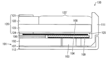
- FIG. 5 is a cross-sectional view of a conventional display device 130.
- the display device 130 includes a backlight unit 101 and a display panel 120.
- the backlight unit 101 includes a light source 103, a light source flexible substrate (hereinafter referred to as a light source FPC (Flexible Printed Circuit)) 104, a light guide plate 102, and a display panel fixing tape 108.
- a light source FPC Flexible Printed Circuit
- the light source 103 is fixed to the light source FPC 104 by adhering to the light source FPC fixing tape 109 having adhesiveness on both sides. In this way, the light source 103 is fixed at a predetermined position with respect to the light guide plate 102.
- the display panel 120 includes a polarizing plate 121, a glass substrate 122, a glass substrate 123, and a polarizing plate 124 in this order from the top.
- a liquid crystal layer (not shown) is formed between the glass substrate 122 and the glass substrate 123. Further, polarizing plates 121 and 124 are arranged so as to sandwich the glass substrates 122 and 123.
- the backlight unit 101 and the display panel 120 are fixed to each other by the display panel fixing tape 108.
- the display panel fixing tape 108 has adhesiveness on both sides, and is adhered to the light source FPC 104 and the polarizing plate 124.
- the display panel fixing tape 108 is not bonded to the protruding portion 123 ′ of the glass substrate 123. That is, a space 125 corresponding to the thickness of the polarizing plate 124 is generated between the display panel fixing tape 108 and the protruding portion 123 ′.
- the display device 130 is configured by incorporating the display panel 120 into the backlight unit 101. During this incorporation, an external pressure may be applied to the display panel 120 in some cases. In such a case, the protrusion 123 ′ may be displaced in the direction of the display panel fixing tape 8 due to the presence of the space 125. As a result, the protrusion 123 ′ and the display panel fixing tape 108 on the upper surface of the light source FPC 104 adhere to each other, causing a phenomenon that the position of the light source 103 mounted on the light source FPC 104 is shifted. When the position of the light source 103 is deviated, the angle of the light incident on the light guide plate 102 is deviated from the angle of the incident light of the light source 103 at a predetermined position. A problem arises that bright lines occur.
- a spacer 205 is disposed between the protruding portion 223 ′ and the display panel fixing tape 208 to prevent the protruding portion 223 ′ and the display panel fixing tape 208 from adhering to each other.
- FIG. 6 is a cross-sectional view of the display device 230 in Patent Document 1.
- the display device 230 includes a display panel 220, a backlight unit 201, and a spacer 205.
- the spacer 205 is provided to prevent the protrusion 223 ′ on the glass substrate 222 and the display panel fixing tape 208 from adhering. Therefore, the spacer 205 is disposed between the protrusion 223 ′ and the display panel fixing tape 208. Further, the thickness of the spacer 205 is set to be substantially equal to that of the polarizing plate 224.
- the display device 230 has such a configuration, thereby preventing the protrusion 223 ′ from being bonded to the display panel fixing tape 208. Therefore, in the display device 230, the position of the light source 103 is shifted, and the angle of the light incident on the light guide plate 202 is not shifted from the angle of the incident light of the light source 203 fixed at a predetermined position. Variation in luminance and generation of bright lines in the display panel 220 can be prevented.
- Patent Document 1 it is necessary to manufacture the spacer 205 dedicated to the display device 230 in order to make the spacer 205 substantially equal in thickness to the polarizing plate 224. That is, in the technique of Patent Document 1, a manufacturing process for manufacturing the spacer 205 is required separately from the manufacturing process of the display device 230. Further, since the spacer 205 is set to have a thickness substantially equal to that of the polarizing plate 224, the choice of the material for the spacer 205 is limited.
- the spacer is disposed on the surface opposite to the surface on which the light source is disposed on the light source substrate of the backlight unit without requiring a step of separately providing a spars. can do.
- a backlight unit that emits light incident from the side surface from the light exit surface;
- a light source disposed on a side surface of the light guide plate;
- the light source is mounted on one surface, and a substrate in which the end of the one surface and the end of the light emitting surface of the light guide plate are in close contact with each other;
- An optical sheet disposed on the light exit surface of the light guide plate;
- a double-sided tape that is affixed to the four sides of the light exit surface of the optical sheet and that is also affixed to the surface opposite to the surface on which the light source is disposed in the substrate; It is arranged so as to cover both the optical sheet and the substrate, and includes a protective film having a cut line along the longitudinal direction of the substrate at a corresponding position between the substrate and the optical sheet. It is characterized by.
- the cut line along the longitudinal direction of the substrate is provided at a corresponding position between the substrate on the protective film and the optical sheet. Therefore, when the protective film is peeled off from the edge of the portion corresponding to the light emitting surface of the optical sheet, only the portion from the edge parallel to the cut line in the portion corresponding to the light emitting surface of the optical sheet is cut off. The As a result, a portion corresponding to the surface opposite to the surface where the light source is disposed on the substrate from the cut line remains. That is, when the display panel is incorporated into the backlight unit, a part of the protective film is interposed between the double-sided tape attached to the surface of the substrate opposite to the surface where the light source is disposed and the glass substrate of the display panel.
- a part of the protective film can be left at a position where the spacer needs to be arranged in order to prevent the positional deviation of the light source due to the adhesion between the double-sided tape and the glass substrate. Can be made.
- the spacer can be arranged by a simple method of peeling off the protective film. Then, by using the backlight unit according to one embodiment of the present invention, a display module in which spacers are arranged can be completed by a simple method. Since the protective film is peeled off in the normal manufacturing process of the display module, it is not necessary to provide a new manufacturing process for manufacturing the spacer in the present invention.
- the display module provides The surface from which the light source in the board
- the backlight unit leaving a part up to the edge parallel to the cut line in the part corresponding to the opposite surface; And a display panel.
- the backlight unit in which the spacers are arranged can be completed by a simple method of peeling off the protective film. Further, by combining the backlight unit and the display panel, it is possible to suppress variation in luminance and generation of bright lines on the display panel.
- the display device includes the display module in order to solve the above-described problems.
- the spacer is arranged between the glass substrate in the display panel and the display panel fixing tape in the backlight unit, the position of the light source does not shift. Therefore, variation in luminance and generation of bright lines on the display panel of the display device can be suppressed.
- a method for manufacturing a display module according to the present invention includes: In the protective film provided in the backlight unit, the portion from the side parallel to the cut line to the cut line in the portion corresponding to the light exit surface of the optical sheet is peeled off, and the light source from the cut line to the substrate A peeling step that leaves a part up to the edge parallel to the cut line in the part corresponding to the surface opposite to the surface where the The backlight unit after the isolation step includes an assembling step for incorporating a display panel.
- the spacer made of a part of the remaining protective film can be arranged on the backlight unit by a simple method of peeling off the protective film. Then, by incorporating a display panel into the backlight unit, a display device module including a spacer can be manufactured without providing a special manufacturing process.
- the part when the protective film is peeled off, by leaving a part on the backlight unit, the part can function as a spacer. That is, the spacer can be arranged by a simple method of peeling off the protective film.
- FIG. 4A is a perspective view of a display panel
- FIG. 4B is a perspective view of a backlight unit
- FIG. 4C is a perspective view of a display device module. It is sectional drawing of the display module which concerns on one Embodiment of this invention. It is sectional drawing of the conventional display apparatus. 10 is a cross-sectional view of a display device in Patent Document 1.
- FIG. 4A is a perspective view of a display panel
- FIG. 4B is a perspective view of a backlight unit
- FIG. 4A is a perspective view of a display panel
- FIG. 4B is a perspective view of a backlight unit
- FIG. 4C is a perspective view of a display device module. It is
- Embodiments relating to the display module of the present invention will be described with reference to FIGS. 1 to 4 as follows. First, the backlight unit 1 will be described with reference to FIG.
- FIG. 1 is a plan view of a backlight unit 1 according to an embodiment of the present invention.
- the backlight 1 includes a backlight case 10, a protective film 5, and a light source FPC 4.
- the backlight case 10 is a case for storing each member constituting the backlight unit 1.
- the light source FPC 4 is a substrate on which a light source 3 to be described later and its drive circuit are mounted.
- the protective film 5 is used for protecting a display panel fixing tape 8 described later.
- the display panel fixing tape 8 has adhesiveness on both sides.
- the protective film 5 prevents dust, dirt, and the like from adhering to the surface of the display panel fixing tape 8 on which the display panel 20 to be described later is mounted, thereby reducing its adhesive strength. Therefore, the protective film 5 is disposed so as to cover the optical sheet 6 and the light source FPC 4 described later so as to be disposed on the surface of the display panel fixing tape 8 on the side where the display panel 20 is mounted. Further, since the protective film 5 temporarily protects the display panel fixing tape 8, it can be peeled off from the display panel fixing tape 8 with a certain amount of force.
- the protective film 5 is provided with a cut line 13. As a result, a spacer 14 described later can be easily disposed in the backlight unit 1. Since the cut line 13 is provided, when the protective film 5 is peeled off, the portion from the edge parallel to the cut line 13 to the cut line 13 in the portion corresponding to the light emission surface of the optical sheet 6 described later is cut. Can be peeled off. At the same time, it is possible to leave a portion from the cut line 13 to an end parallel to the cut line 13 in a portion corresponding to the surface opposite to the surface on which the light source 3 is disposed in the light source FPC 4.
- the protective film 5 is not peeled off entirely, but peeled off so as to leave a part thereof, and the remaining part. Can function as the spacer 14.
- the cut line 13 is provided along the longitudinal direction of the light source FPC 4 at a position corresponding to between the light source FPC 4 and the optical sheet 6.
- the protective film 5 described later is peeled off, the protective film is provided at a position where a spacer needs to be disposed in order to prevent displacement of the light source 3 due to adhesion between the display panel fixing tape 8 and a glass substrate 24 described later. Since a part of 5 can be left, the remaining part can function as the spacer 14.
- the cut line 13 is provided in the protective film 5 before the protective film 5 is attached to the backlight unit 1.
- the protective film 5 is provided by half-cutting using a mold or the like. According to this method, the protective film 5 is not completely cut. Therefore, when the protective film 5 is affixed to the backlight unit 1, the part functioning as the spacer 14 and the other part can be affixed together. On the other hand, when part of the protective film 5 is peeled from the backlight unit 1, only the part other than the part that functions as the spacer 14 can be easily peeled off.
- FIG. 2 is a diagram for illustrating a method of arranging the spacers 14.
- A) of the figure is a figure which shows a mode that the protective film 5 is peeled
- (b) of the figure is a figure which shows a mode after peeling the protective film 5.
- the protective film 5 is peeled off from the upper surface of the display panel fixing tape 8 as shown in FIG. Then, since the cut line 13 is provided on the protective film 5, the part from the end side parallel to the cut line 13 to the cut line 13 in the part corresponding to the light emission surface of the optical sheet 6 can be peeled off. it can. Moreover, the part from the cut line 13 to the edge parallel to the cut line 13 in the part corresponding to the surface opposite to the surface on which the light source 3 is disposed in the light source FPC 4 can be left.
- the position where the protective film 5 remains is a position where a spacer needs to be disposed in order to prevent the positional deviation of the light source 3 due to the adhesion between the display panel fixing tape 8 and the glass substrate 24. Therefore, the remaining part of the protective film 5 can be used as the spacer 14.
- the spacers 14 can be arranged by a simple method of peeling off the protective film 5. Moreover, since peeling of a protective film is made in the manufacturing process of a normal display module, the spacer 14 can be arrange
- the backlight unit 1 includes a backlight case 10, a light source FPC 4, an optical sheet 6, a display panel fixing tape 8, and a spacer 14. Since the backlight unit 1 includes the spacer 14, when the display panel 20 is assembled, the display panel fixing tape 8 and a protrusion 23 ′ described later can be prevented from adhering. That is, the position of the light source 3 does not shift due to the bonding between the protrusion 23 ′ and the display panel fixing tape 8. Therefore, by manufacturing the display module 30 using the backlight unit 1, variations in luminance of the display panel 20 can be suppressed.
- FIG. 3 is a diagram for illustrating a process of incorporating the display panel into the backlight unit 1.
- 4A is a perspective view of the display panel 20
- FIG. 4B is a perspective view of the backlight unit 1
- FIG. 4C is a perspective view of the display module 30.
- the display module 30 is completed by incorporating the display panel 20 into the backlight unit 1.
- the display panel 20 includes a polarizing plate 21, a glass substrate 22, a glass substrate 23, and a polarizing plate 24. Details will be described later.
- the backlight unit 1 includes a spacer 5.
- the spacer 5 is a position corresponding to the upper surface of the light source 3 and is provided at a position corresponding to the lower surface of the protrusion 23 ′ when the display panel 20 is assembled.
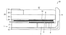
- FIG. 4 is a cross-sectional view of the display module 30.
- the display module 30 includes a display panel 20 on the upper surface of the backlight unit 1. (Cross section of display panel 20)
- a liquid crystal layer (not shown) is provided between the glass substrate 22 and the glass substrate 23.
- the display panel 20 is provided with a polarizing plate 21 and a polarizing plate 24 so as to sandwich the glass substrate 22 and the glass substrate 23.
- the glass substrate 23 includes a protrusion 23 ′ for mounting a drive circuit.
- the backlight unit 1 includes a light source 3, a light source FPC 4, and a light guide plate 2.
- the light source 3 for example, an LED (Light Emitting Diode) can be used.
- the light source 3 is disposed on the side surface of the light guide plate 2.
- the light source 3 is mounted on the light source FPC 4 by adhering to the light source FPC fixing tape 9 having adhesiveness on both sides.
- the light source FPC 4 is fixed to the frame 11 using a light source FPC fixing tape 9. Further, the light source FPC 4 and the light guide plate 2 are in close contact so that the end of the surface on which the light source 3 is mounted in the light source FPC 4 and the end of the light emitting surface of the light guide plate 2 face each other.
- the light guide plate 2 changes the optical path of the light emitted from the light source 3 in the direction of the optical sheet 6.
- An optical sheet 6 is disposed on the light exit surface of the light guide plate 2. The optical sheet 6 diffuses the irradiation light so as to have a uniform luminance with respect to the display panel 20 and increases the luminance of the irradiation light.
- a reflection sheet 7 is disposed on the surface of the light guide plate 2 opposite to the light exit surface. The reflection sheet 7 reflects light that has not entered the light guide plate 2 out of the light emitted from the light source 3 in the direction of the light guide plate 2.
- the display panel fixing tape 8 is a tape for fixing the display panel 20 to the frame 11 via the light source FPC 4. As described above, the display panel fixing tape 8 is a double-sided tape having adhesiveness on both sides. As shown in FIGS. 2 and 4, the display panel fixing tape 8 is affixed to the four sides of the light emission surface of the optical sheet 6 and on the surface opposite to the surface on which the light source 3 is disposed in the light source FPC 4. Is also affixed. On the other hand, the display panel fixing tape 8 is not attached to the central portion of the light emission surface of the optical sheet 6. As shown in FIG. 4, the display panel fixing tape 8 is bonded to the polarizing plate 24, the optical sheet 6, and the light source FPC 4.
- the spacer 14 is used to prevent adhesion between the display panel fixing tape 8 and the protrusion 23 ′. Therefore, it is disposed between the protrusion 23 ′ and the display panel fixing tape 8. As described above, the spacer 14 is a part of the protective film 5.
- the backlight unit of the present invention can be used as a display module component.
- the display module of this invention can be utilized as components of a display apparatus.
- the display device of the present invention can be widely used in combination with various electronic devices such as a television and a personal computer.
Landscapes
- Physics & Mathematics (AREA)
- Liquid Crystal (AREA)
- General Physics & Mathematics (AREA)
- Optics & Photonics (AREA)
Abstract
バックライトユニット(1)は、光源を一方の面に実装すると共に、当該一方の面の端部と導光板の光出射面の端部とが互いに向き合うように密着されている基板4と、導光板における光出射面に配置されている光学シート(6)と、光学シート(6)の光出射面における四辺に貼付されていると共に、基板(4)における光源が配置されている面と反対の面にも貼付されている表示パネル固定テープ(8)と、光学シート(6)および基板(4)を共に覆うように配置されており、基板(4)と光学シート6との間に対応する位置において基板(4)における長手方向に沿ったカットライン13を有する保護フィルム5とを備えている。この構成によって、スパーサ(14)を別途設ける工程を必要とせずに、バックライトユニット(1)の基板(4)における光源が配置されている面と反対の面にスペーサ(14)を配置する。
Description
本発明は、バックライトユニットにおける保護フィルムの一部をスペーサとして用いた表示装置に関する。
近年、様々な電子機器に表示装置が使用されている。当該表示装置における表示パネルを照射する方法としてバックライトユニットを用いる方法がある。バックライトユニットは、一般に、光源と、当該光源からの光を表示パネルの背面に照射する導光板と、当該導光板から出射した光を拡散させる拡散シートとを備えている。光源から導光板へ入射した光は、導光板における光出射面と光反射面との間において反射を繰り返した後に、光出射面から表示パネルの背面側へ出射する。
以下に、バックライトユニットを備えた従来の表示装置の構成を説明する。図5は、従来の表示装置130の断面図である。同図に示すとおり、表示装置130は、バックライトユニット101と表示パネル120とを備えている。バックライトユニット101は、光源103と、光源用フレキシブル基板(以下、光源用FPC(Flexible Printed Circuit)と呼ぶ。)104と、導光板102と、表示パネル固定テープ108とを備えている。
光源103は、両面に粘着性を有する光源用FPC固定テープ109に接着することにより、光源用FPC104に固定される。このようにして、光源103は、導光板102に対する所定の位置に固定される。また、表示パネル120は、上面から順に、偏光板121と、ガラス基板122と、ガラス基板123と、偏光板124とを備えている。ガラス基板122とガラス基板123との間には、液晶層(不図示)が形成されている。また、ガラス基板122および123を挟むように偏光板121および124が配置されている。
バックライトユニット101と表示パネル120とは、表示パネル固定テープ108によって、互いに固定される。表示パネル固定テープ108は、両面に粘着性を有しており、光源用FPC104と偏光板124とに接着している。一方、表示パネル固定テープ108は、ガラス基板123における突出部123’には接着していない。すなわち、表示パネル固定テープ108と突出部123’との間には、偏光板124の厚さに相当する分だけの空間125が生じている。
表示装置130は、バックライトユニット101に表示パネル120を組み込むことにより構成される。この組み込みの際に、表示パネル120に外圧が加わってしまう場合がある。そのような場合、空間125があることにより、突起部123’が表示パネル固定テープ8の方向にずれることがある。そうすると、突出部123’と光源用FPC104上面の表示パネル固定テープ108とが接着して、光源用FPC104に実装された光源103の位置がずれる現象が生じてしまう。光源103の位置がずれると、所定の位置にある光源103の入射光の角度に対して、導光板102に入射される光の角度がずれてしまい、その結果、表示パネル120に輝度のばらつきや輝線が生じるという問題が生ずる。
そこで、下記特許文献1においては、突出部223’と表示パネル固定テープ208との間にスペーサ205を配置して、突出部223’と表示パネル固定テープ208とが接着することを防いでいる。
以下、下記特許文献1における表示装置230の構成を説明する。図6は、特許文献1における表示装置230の断面図である。同図に示すように、表示装置230は、表示パネル220とバックライトユニット201とスペーサ205とを備えている。
スペーサ205は、ガラス基板222における突出部223’と、表示パネル固定テープ208との接着を防ぐために設けられる。そのため、スペーサ205は、突出部223’と表示パネル固定テープ208との間に配置されている。また、スペーサ205の厚さは、偏光板224と略等しい厚さに設定されている。表示装置230は、このような構成を有することにより、突出部223’と、表示パネル固定テープ208との接着を防いでいる。したがって、表示装置230においては、光源103の位置がずれて、所定の位置に固定される光源203の入射光の角度に対して、導光板202に入射される光の角度がずれることはなく、表示パネル220における輝度のばらつきや輝線の発生を防止することできる。
しかしながら、上記特許文献1においては、スペーサ205を偏光板224と略等しい厚さにするため、表示装置230専用のスペーサ205を製造する必要がある。すなわち、上記特許文献1の技術においては、表示装置230の製造工程とは別に、スペーサ205を製造するための製造工程が必要である。また、スペーサ205を偏光板224と略等しい厚さに設定するために、スペーサ205の材料の選択肢が限られてしまう。
本発明は上記の課題を解決するために為されたものである。そして、本発明の一態様に係るバックライトユニットによれば、スパーサを別途設ける工程を必要とせずに、バックライトユニットの光源用基板における光源が配置されている面と反対の面にスペーサを配置することができる。
上記の課題を解決するために、本発明の一態様に係るバックライトユニットは、
側面から入射した光を光出射面から出射させる導光板と、
上記導光板の側面に配置されている光源と、
上記光源を一方の面に実装すると共に、当該一方の面の端部と上記導光板の光出射面の端部とが互いに向き合うように密着されている基板と、
上記導光板における光出射面に配置されている光学シートと、
上記光学シートの光出射面における四辺に貼付されていると共に、上記基板における光源が配置されている面と反対の面にも貼付されている両面テープと、
上記光学シートおよび上記基板を共に覆うように配置されており、上記基板と上記光学シートとの間に対応する位置において上記基板における長手方向に沿ったカットラインを有する保護フィルムとを備えていることを特徴としている。
側面から入射した光を光出射面から出射させる導光板と、
上記導光板の側面に配置されている光源と、
上記光源を一方の面に実装すると共に、当該一方の面の端部と上記導光板の光出射面の端部とが互いに向き合うように密着されている基板と、
上記導光板における光出射面に配置されている光学シートと、
上記光学シートの光出射面における四辺に貼付されていると共に、上記基板における光源が配置されている面と反対の面にも貼付されている両面テープと、
上記光学シートおよび上記基板を共に覆うように配置されており、上記基板と上記光学シートとの間に対応する位置において上記基板における長手方向に沿ったカットラインを有する保護フィルムとを備えていることを特徴としている。
上記構成によれば、保護フィルム上の基板と光学シートとの間に対応する位置に、基板における長手方向に沿ったカットラインが設けられている。したがって、保護フィルムを光学シートの光出射面に対応する部分の端辺から剥離すると、光学シートの光出射面に対応する部分におけるカットラインと平行な端辺からカットラインまでの部分のみが剥離される。この結果、カットラインから基板における光源が配置されている面と反対の面に対応する部分が残る。すなわち、バックライトユニットに表示パネルを組み込む際に、基板における光源が配置されている面と反対の面に貼付されている両面テープと、表示パネルにおけるガラス基板との間に、保護フィルムの一部が残る。つまり、両面テープとガラス基板との接着による光源の位置ずれを防ぐためにスペーサを配置する必要がある位置に、保護フィルムの一部を残すことができるため、当該保護フィルムの一部をスペーサとして機能させることができる。
上述のように、本発明の一態様に係るバックライトユニットでは、保護フィルムを剥離するという簡単な方法によって、スペーサを配置することができる。そして、本発明の一態様に係るに係るバックライトユニットを用いることによって、簡単な方法でスペーサを配置した表示モジュールを完成させることができる。保護フィルムの剥離は、通常の表示モジュールの製造過程においてなされるものであるから、本発明においてスペーサを製造するための新たな製造工程を設ける必要もない。
本発明に係る表示モジュールは、上記の課題を解決するために、
上記保護フィルムを、上記光学シートの光出射面に対応する部分における上記カットラインと平行な端辺から上記カットラインまでの部分を剥離して、上記カットラインから基板における光源が配置されている面と反対の面に対応する部分における上記カットラインと平行な端辺までの部分を残した上記バックライトユニットと、
表示パネルとを備えていることを特徴としている。
上記構成によれば、保護フィルムを剥離するという簡単な方法により、スペーサを配置したバックライトユニットを完成させることができる。また、当該バックライトユニットと表示パネルとを組み合わせることにより、表示パネル上の輝度のばらつきや輝線の発生を抑制することができる。
本発明に係る表示装置は、上記の課題を解決するために、上記表示モジュールを備えていることを特徴としている。
上記構成によれば、表示パネルにおけるガラス基板と、バックライトユニットにおける表示パネル固定テープとの間に、スペーサが配置されているため、光源の位置がずれることはない。よって、表示装置の表示パネル上の輝度のばらつきや輝線の発生を抑制することができる。
本発明に係る表示モジュールの製造方法は、
上記バックライトユニットが備える上記保護フィルムにおける、上記光学シートの光出射面に対応する部分における上記カットラインと平行な端辺から上記カットラインまでの部分を剥離すると共に、上記カットラインから基板における光源が配置されている面と反対の面に対応する部分における上記カットラインと平行な端辺までの部分を残す剥離工程と、
上記隔離工程後の上記バックライトユニットに、表示パネルを組み込む組込工程とを備えていることを特徴としている。
上記バックライトユニットが備える上記保護フィルムにおける、上記光学シートの光出射面に対応する部分における上記カットラインと平行な端辺から上記カットラインまでの部分を剥離すると共に、上記カットラインから基板における光源が配置されている面と反対の面に対応する部分における上記カットラインと平行な端辺までの部分を残す剥離工程と、
上記隔離工程後の上記バックライトユニットに、表示パネルを組み込む組込工程とを備えていることを特徴としている。
上記構成によれば、保護フィルムを剥離するという簡単な方法により、バックライトユニット上に、残された保護フィルムの一部からなるスペーサを配置することができる。そして、当該バックライトユニットに表示パネルを組み込むことにより、特別な製造工程を設けることなくスペーサを備えた表示装置モジュールを製造することができる。
本発明は、保護フィルムを剥離する際に、一部をバックライトユニット上に残すことによって、当該一部をスペーサとして機能させることができる。すなわち、保護フィルムを剥離するという簡単な方法によってスペーサを配置することができるという効果を奏する。
以下、本発明の一実施形態について、詳細に説明する。
本発明の表示モジュールに関する実施形態について図1~4に基づいて説明すれば以下のとおりである。まず、バックライトユニット1について図1を用いて説明する。
(バックライトユニット1)
図1は、本発明の一実施形態に係るバックライトユニット1の平面図である。同図においては、説明の便宜のため、バックライトユニット1の概略を示す。同図に示すように、バックライト1は、バックライトケース10と、保護フィルム5と、光源用FPC4とを備えている。バックライトケース10は、バックライトユニット1を構成する各部材を収納するケースである。光源用FPC4は、後述する光源3とその駆動回路とを実装する基板である。
(保護フィルム5)
保護フィルム5は、後述する表示パネル固定テープ8を保護するために用いられる。表示パネル固定テープ8は、両面に粘着性を有している。保護フィルム5は、表示パネル固定テープ8における後述する表示パネル20を実装する側の面にゴミや汚れ等が付着して、その粘着力が低下することを、防止する。そのため、保護フィルム5は、表示パネル固定テープ8の表示パネル20を実装する側の面に配置されるように、後述する光学シート6および光源用FPC4を覆うように配置される。また、保護フィルム5は、一時的に表示パネル固定テープ8を保護するものであるので、ある程度の力によって、表示パネル固定テープ8から剥離することができる。
図1は、本発明の一実施形態に係るバックライトユニット1の平面図である。同図においては、説明の便宜のため、バックライトユニット1の概略を示す。同図に示すように、バックライト1は、バックライトケース10と、保護フィルム5と、光源用FPC4とを備えている。バックライトケース10は、バックライトユニット1を構成する各部材を収納するケースである。光源用FPC4は、後述する光源3とその駆動回路とを実装する基板である。
(保護フィルム5)
保護フィルム5は、後述する表示パネル固定テープ8を保護するために用いられる。表示パネル固定テープ8は、両面に粘着性を有している。保護フィルム5は、表示パネル固定テープ8における後述する表示パネル20を実装する側の面にゴミや汚れ等が付着して、その粘着力が低下することを、防止する。そのため、保護フィルム5は、表示パネル固定テープ8の表示パネル20を実装する側の面に配置されるように、後述する光学シート6および光源用FPC4を覆うように配置される。また、保護フィルム5は、一時的に表示パネル固定テープ8を保護するものであるので、ある程度の力によって、表示パネル固定テープ8から剥離することができる。
(カットライン13)
図1に示すように、保護フィルム5にはカットライン13が設けられている。このことによって、バックライトユニット1に、後述するスペーサ14を容易に配置することができる。カットライン13が設けられていることによって、保護フィルム5を剥離する際に、後述する光学シート6の光出射面に対応する部分におけるカットライン13と平行な端辺からカットライン13までの部分を剥離することができる。同時に、カットライン13から光源用FPC4における光源3が配置されている面と反対の面に対応する部分におけるカットライン13と平行な端辺までの部分を残すことができる。
図1に示すように、保護フィルム5にはカットライン13が設けられている。このことによって、バックライトユニット1に、後述するスペーサ14を容易に配置することができる。カットライン13が設けられていることによって、保護フィルム5を剥離する際に、後述する光学シート6の光出射面に対応する部分におけるカットライン13と平行な端辺からカットライン13までの部分を剥離することができる。同時に、カットライン13から光源用FPC4における光源3が配置されている面と反対の面に対応する部分におけるカットライン13と平行な端辺までの部分を残すことができる。
従来の表示装置モジュールを製造する過程において、バックライトユニットに表示パネルを組み込む際、保護フィルムは、全て剥離されてしまう。しかし、本発明の一実施形態においては、保護フィルム5にカットライン13を設けているため、保護フィルム5を全て剥離するのではなく、その一部を残すように剥離して、残された部分をスペーサ14として機能させることが可能となる。
カットライン13は、光源用FPC4と光学シート6との間に対応する位置において、光源用FPC4における長手方向に沿って設けられる。このことにより、後述する保護フィルム5の剥離の際に、表示パネル固定テープ8と後述するガラス基板24との接着による光源3の位置ずれを防ぐためにスペーサを配置する必要がある位置に、保護フィルム5の一部を残すことができるため、当該残された一部をスペーサ14として機能させることができる。
カットライン13は、保護フィルム5をバックライトユニット1に貼付する前に、保護フィルム5に設けられる。例えば、金型等を使用して、保護フィルム5にハーフカットを入れることにより設けられる。この手法によれば、保護フィルム5は完全にはカットされていない。したがって、保護フィルム5をバックライトユニット1に貼付する際には、スペーサ14として機能させる部分とその他の部分とを一緒に貼付することができる。一方、バックライトユニット1から保護フィルム5の一部を剥離する際には、スペーサ14として機能させる部分以外の部分のみを、容易に剥離することができる。
(スペーサ14の配置方法)
次に、スペーサ14の配置方法を図2を用いて説明する。図2は、スペーサ14の配置方法を示すための図である。同図の(a)は、保護フィルム5を剥離する様子を示す図であり、同図の(b)は、保護フィルム5を剥離した後の様子を示す図である。
次に、スペーサ14の配置方法を図2を用いて説明する。図2は、スペーサ14の配置方法を示すための図である。同図の(a)は、保護フィルム5を剥離する様子を示す図であり、同図の(b)は、保護フィルム5を剥離した後の様子を示す図である。
同図の(a)に示すように、保護フィルム5を表示パネル固定テープ8の上面から剥離する。そうすると、保護フィルム5上にカットライン13が設けられているために、光学シート6の光出射面に対応する部分におけるカットライン13と平行な端辺からカットライン13までの部分を剥離することができる。また、カットライン13から光源用FPC4における光源3が配置されている面と反対の面に対応する部分におけるカットライン13と平行な端辺までの部分は、残すことができる。当該保護フィルム5が残った位置は、表示パネル固定テープ8とガラス基板24との接着による光源3の位置ずれを防ぐためにスペーサを配置する必要がある位置である。したがって、当該保護フィルム5の残した部分をスペーサ14として用いることができる。
このように、本発明の一実施形態に係るバックライトユニット1では、保護フィルム5を剥離するという簡単な方法によって、スペーサ14を配置することができる。また、保護フィルムの剥離は、通常の表示モジュールの製造過程においてなされるものであるから、これまでの製造工程に新たな工程を設けることを必要とせずに、スペーサ14を配置することができる。
(保護フィルム5を剥離した後のバックライトユニット1)
図2(b)に示すように、バックライトユニット1は、バックライトケース10と、光源用FPC4と、光学シート6と、表示パネル固定テープ8と、スペーサ14とを備えている。バックライトユニット1は、スペーサ14を備えているので、表示パネル20を組み込む時に、表示パネル固定テープ8と後述する突起部23’とが接着することを防止することができる。すなわち、突起部23’と表示パネル固定テープ8とが接着することにより光源3の位置がずれることはない。したがって、バックライトユニット1を用いて表示モジュール30を製造することによって、表示パネル20の輝度のばらつきを抑制することができる。
図2(b)に示すように、バックライトユニット1は、バックライトケース10と、光源用FPC4と、光学シート6と、表示パネル固定テープ8と、スペーサ14とを備えている。バックライトユニット1は、スペーサ14を備えているので、表示パネル20を組み込む時に、表示パネル固定テープ8と後述する突起部23’とが接着することを防止することができる。すなわち、突起部23’と表示パネル固定テープ8とが接着することにより光源3の位置がずれることはない。したがって、バックライトユニット1を用いて表示モジュール30を製造することによって、表示パネル20の輝度のばらつきを抑制することができる。
(表示モジュール30)
バックライトユニット1に表示パネルを組み込む工程を、図3を用いて説明する。図3は、バックライトユニット1に表示パネルを組み込む工程を示すための図である。同図の(a)は表示パネル20の斜視図であり、同図の(b)はバックライトユニット1の斜視図であり、同図の(c)は表示モジュール30の斜視図である。同図の(c)に示すように、表示モジュール30は、バックライトユニット1に表示パネル20を組み込むことによって完成する。
バックライトユニット1に表示パネルを組み込む工程を、図3を用いて説明する。図3は、バックライトユニット1に表示パネルを組み込む工程を示すための図である。同図の(a)は表示パネル20の斜視図であり、同図の(b)はバックライトユニット1の斜視図であり、同図の(c)は表示モジュール30の斜視図である。同図の(c)に示すように、表示モジュール30は、バックライトユニット1に表示パネル20を組み込むことによって完成する。
(表示パネル20)
図3の(a)に示すとおり、表示パネル20は、偏光板21と、ガラス基板22と、ガラス基板23と、偏光板24とを備えている。詳細は後述する。
図3の(a)に示すとおり、表示パネル20は、偏光板21と、ガラス基板22と、ガラス基板23と、偏光板24とを備えている。詳細は後述する。
(バックライトユニット1)
図3の(b)に示すとおり、バックライトユニット1はスペーサ5を備えている。スペーサ5は、光源3の上面に相当する位置であり、かつ、表示パネル20を組み込む際に、突起部23’の下面に相当する位置に設けられる。
図3の(b)に示すとおり、バックライトユニット1はスペーサ5を備えている。スペーサ5は、光源3の上面に相当する位置であり、かつ、表示パネル20を組み込む際に、突起部23’の下面に相当する位置に設けられる。
(表示モジュール30の構成)
図4を参照して、表示モジュール30の構成について説明する。図4は、表示モジュール30の断面図である。同図に示すように、表示モジュール30は、バックライトユニット1の上面に表示パネル20を備えている。
(表示パネル20の断面)
表示パネル20において、ガラス基板22とガラス基板23との間には、図示しない液晶層が設けられている。図4に示すように、表示パネル20には、ガラス基板22およびガラス基板23を挟むように、偏光板21と偏光板24とが設けられている。また、ガラス基板23は、駆動回路を実装する突起部23’を備えている。
図4を参照して、表示モジュール30の構成について説明する。図4は、表示モジュール30の断面図である。同図に示すように、表示モジュール30は、バックライトユニット1の上面に表示パネル20を備えている。
(表示パネル20の断面)
表示パネル20において、ガラス基板22とガラス基板23との間には、図示しない液晶層が設けられている。図4に示すように、表示パネル20には、ガラス基板22およびガラス基板23を挟むように、偏光板21と偏光板24とが設けられている。また、ガラス基板23は、駆動回路を実装する突起部23’を備えている。
(バックライトユニット1の断面)
図4に示すように、バックライトユニット1は、光源3と、光源用FPC4と、導光板2とを備えている。光源3としては、例えば、LED(Light Emitting Diode)を用いることができる。光源3は、導光板2の側面に配置されている。光源3は、両面に粘着性を有する光源用FPC固定テープ9に接着することによって、光源用FPC4に実装される。光源用FPC4は、光源用FPC固定テープ9を用いてフレーム11に固定される。また、光源用FPC4および導光板2は、光源用FPC4における光源3を実装する面の端部と導光板2における光出射面の端部とが互いに向き合うように密着している。
図4に示すように、バックライトユニット1は、光源3と、光源用FPC4と、導光板2とを備えている。光源3としては、例えば、LED(Light Emitting Diode)を用いることができる。光源3は、導光板2の側面に配置されている。光源3は、両面に粘着性を有する光源用FPC固定テープ9に接着することによって、光源用FPC4に実装される。光源用FPC4は、光源用FPC固定テープ9を用いてフレーム11に固定される。また、光源用FPC4および導光板2は、光源用FPC4における光源3を実装する面の端部と導光板2における光出射面の端部とが互いに向き合うように密着している。
(導光板2)
導光板2は、光源3から照射された光の光路を、光学シート6の方向へ変化させる。導光板2の光出射面には、光学シート6が配置されている。光学シート6は、表示パネル20に対して均一輝度を有するように照射光を拡散させて、その照射光の輝度を増加させる。また、導光板2の光出射面と反対の面には、反射シート7が配置されている。反射シート7は、光源3から照射された光のうち導光板2に入射しなかった光を導光板2の方向に反射させる。
導光板2は、光源3から照射された光の光路を、光学シート6の方向へ変化させる。導光板2の光出射面には、光学シート6が配置されている。光学シート6は、表示パネル20に対して均一輝度を有するように照射光を拡散させて、その照射光の輝度を増加させる。また、導光板2の光出射面と反対の面には、反射シート7が配置されている。反射シート7は、光源3から照射された光のうち導光板2に入射しなかった光を導光板2の方向に反射させる。
(表示パネル固定テープ8)
表示パネル固定テープ8は、表示パネル20を、光源用FPC4を介してフレーム11に固定するためのテープである。上述したように、表示パネル固定テープ8は、両面に粘着性を有する両面テープである。図2および図4に示すように、表示パネル固定テープ8は、光学シート6の光出射面における四辺に貼付されていると共に、光源用FPC4における光源3が配置されている面と反対の面にも貼付されている。一方、表示パネル固定テープ8は、光学シート6の光出射面における中心部には、貼付されていない。図4に示すように、表示パネル固定テープ8は、偏光板24と、光学シート6と、光源用FPC4とに接着している。
表示パネル固定テープ8は、表示パネル20を、光源用FPC4を介してフレーム11に固定するためのテープである。上述したように、表示パネル固定テープ8は、両面に粘着性を有する両面テープである。図2および図4に示すように、表示パネル固定テープ8は、光学シート6の光出射面における四辺に貼付されていると共に、光源用FPC4における光源3が配置されている面と反対の面にも貼付されている。一方、表示パネル固定テープ8は、光学シート6の光出射面における中心部には、貼付されていない。図4に示すように、表示パネル固定テープ8は、偏光板24と、光学シート6と、光源用FPC4とに接着している。
(スペーサ14)
スペーサ14は、表示パネル固定テープ8と突起部23’との接着を防ぐために用いられる。そのため、突起部23’と表示パネル固定テープ8との間に配置される。上述したように、スペーサ14は保護フィルム5の一部である。
スペーサ14は、表示パネル固定テープ8と突起部23’との接着を防ぐために用いられる。そのため、突起部23’と表示パネル固定テープ8との間に配置される。上述したように、スペーサ14は保護フィルム5の一部である。
(本実施形態における効果)
本実施形態においては、保護フィルム5にカットライン13を設けられているので、保護フィルム5を剥離する際、大部分は剥離されるが、残りの一部は剥離されずに残る。これにより、保護フィルム5を剥離するという簡単な方法によって、残された一部からなるスペーサ14をバックライトユニット1に配置することができる。さらに、保護フィルムの剥離は通常の表示モジュールの製造過程においてなされていたものであるから、新たな製造工程を設ける必要もない。また、スペーサ14を偏光板24と略等しい厚さに設定する必要がないため、スペーサ14の材料の選択肢が限られることはない。
本実施形態においては、保護フィルム5にカットライン13を設けられているので、保護フィルム5を剥離する際、大部分は剥離されるが、残りの一部は剥離されずに残る。これにより、保護フィルム5を剥離するという簡単な方法によって、残された一部からなるスペーサ14をバックライトユニット1に配置することができる。さらに、保護フィルムの剥離は通常の表示モジュールの製造過程においてなされていたものであるから、新たな製造工程を設ける必要もない。また、スペーサ14を偏光板24と略等しい厚さに設定する必要がないため、スペーサ14の材料の選択肢が限られることはない。
そして、バックライトユニット1に表示パネル20を組み込む組込工程の際に、表示パネル20に外圧が加わり、突起部23’が表示パネル固定テープ8の方向にずれた場合においても、突起部23’と表示パネル固定テープ6との間にスペーサ14が配置されているために、突起部23’と表示パネル固定テープ6とが接着することを防ぐことができる。したがって、突起部23’と表示パネル固定テープ8とが接着することに伴う光源3の位置ずれも発生することもないので、表示パネル20における輝度のばらつきや輝線の発生を防止することできる。
本発明は上述した各実施形態に限定されるものではなく、請求項に示した範囲で種々の変更が可能であり、異なる実施形態にそれぞれ開示された技術的手段を適宜組み合わせて得られる実施形態についても本発明の技術的範囲に含まれる。
本発明の他の目的、特徴、および優れた点は、以下に示す記載によって十分分かるであろう。また、本発明の利点は、添付図面を参照した次の説明で明白になるであろう。
本発明のバックライトユニットは、表示モジュールの部品として利用できる。そして、本発明の表示モジュールは、表示装置の部品として利用できる。さらに、本発明の表示装置は、テレビおよびパソコン等の各種の電子機器と組み合わせて幅広く利用できる。
1 バックライトユニット
2 導光板
3 光源
4 光源用FPC
5 保護フィルム
6 光学シート
7 反射シート
8 表示パネル固定テープ
9 光源用FPC固定テープ
10 バックライトケース
11 フレーム
13 カットライン
20 表示パネル
21 偏光板
22 ガラス基板
23 ガラス基板
24 偏光板
30 表示モジュール
130 従来の表示装置
230 特許文献1の表示装置
2 導光板
3 光源
4 光源用FPC
5 保護フィルム
6 光学シート
7 反射シート
8 表示パネル固定テープ
9 光源用FPC固定テープ
10 バックライトケース
11 フレーム
13 カットライン
20 表示パネル
21 偏光板
22 ガラス基板
23 ガラス基板
24 偏光板
30 表示モジュール
130 従来の表示装置
230 特許文献1の表示装置
Claims (4)
- 側面から入射した光を光出射面から出射させる導光板と、
上記導光板の側面に配置されている光源と、
上記光源を一方の面に実装すると共に、当該一方の面の端部と上記導光板の光出射面の端部とが互いに向き合うように密着されている基板と、
上記導光板における光出射面に配置されている光学シートと、
上記光学シートの光出射面における四辺に貼付されていると共に、上記基板における光源が配置されている面と反対の面にも貼付されている両面テープと、
上記光学シートおよび上記基板を共に覆うように配置されており、上記基板と上記光学シートとの間に対応する位置において上記基板における長手方向に沿ったカットラインを有する保護フィルムとを備えていることを特徴とするバックライトユニット。 - 上記保護フィルムを、上記光学シートの光出射面に対応する部分における上記カットラインと平行な端辺から上記カットラインまでの部分を剥離して、上記カットラインから基板における光源が配置されている面と反対の面に対応する部分における上記カットラインと平行な端辺までの部分を残した請求項1に記載のバックライトユニットと、
表示パネルとを備えていることを特徴とする表示モジュール。 - 請求項2に記載の表示モジュールを備えていることを特徴とする表示装置。
- 請求項1に記載のバックライトユニットが備える上記保護フィルムにおける、上記光学シートの光出射面に対応する部分における上記カットラインと平行な端辺から上記カットラインまでの部分を剥離すると共に、上記カットラインから基板における光源が配置されている面と反対の面に対応する部分における上記カットラインと平行な端辺までの部分を残す剥離工程と、
上記剥離工程後の上記バックライトユニットに、表示パネルを組み込む組込工程とを備えていることを特徴とする表示モジュールの製造方法。
Applications Claiming Priority (2)
| Application Number | Priority Date | Filing Date | Title |
|---|---|---|---|
| JP2011-089457 | 2011-04-13 | ||
| JP2011089457 | 2011-04-13 |
Publications (1)
| Publication Number | Publication Date |
|---|---|
| WO2012141146A1 true WO2012141146A1 (ja) | 2012-10-18 |
Family
ID=47009319
Family Applications (1)
| Application Number | Title | Priority Date | Filing Date |
|---|---|---|---|
| PCT/JP2012/059723 Ceased WO2012141146A1 (ja) | 2011-04-13 | 2012-04-09 | バックライトユニット、表示モジュール、表示装置および表示モジュールの製造方法 |
Country Status (1)
| Country | Link |
|---|---|
| WO (1) | WO2012141146A1 (ja) |
Citations (2)
| Publication number | Priority date | Publication date | Assignee | Title |
|---|---|---|---|---|
| JP2009025602A (ja) * | 2007-07-20 | 2009-02-05 | Citizen Electronics Co Ltd | 液晶セル接着用両面粘着テープ及びバックライトユニット及び液晶表示装置及び液晶表示装置の製造方法 |
| JP2009098556A (ja) * | 2007-10-19 | 2009-05-07 | Nec Lcd Technologies Ltd | 表示装置 |
-
2012
- 2012-04-09 WO PCT/JP2012/059723 patent/WO2012141146A1/ja not_active Ceased
Patent Citations (2)
| Publication number | Priority date | Publication date | Assignee | Title |
|---|---|---|---|---|
| JP2009025602A (ja) * | 2007-07-20 | 2009-02-05 | Citizen Electronics Co Ltd | 液晶セル接着用両面粘着テープ及びバックライトユニット及び液晶表示装置及び液晶表示装置の製造方法 |
| JP2009098556A (ja) * | 2007-10-19 | 2009-05-07 | Nec Lcd Technologies Ltd | 表示装置 |
Similar Documents
| Publication | Publication Date | Title |
|---|---|---|
| CN101231405B (zh) | 带触摸板的显示组件 | |
| JP5734145B2 (ja) | 面状照明装置 | |
| JP6412721B2 (ja) | 液晶表示装置 | |
| JP2010134004A (ja) | 表示装置 | |
| CN101655636B (zh) | 侧边入光式背光模块、液晶显示装置及其组装方法 | |
| JP5646744B2 (ja) | 表示モジュール及び該モジュールを備えた表示装置 | |
| WO2013161241A1 (ja) | バックライトユニット及び液晶表示装置 | |
| TW201616186A (zh) | 顯示器模組 | |
| KR101630342B1 (ko) | 액정 표시장치 및 그 조립방법 | |
| WO2013118475A1 (ja) | 表示装置 | |
| JP7129286B2 (ja) | 表示装置及びその製造方法 | |
| JP3215799U (ja) | 光学レンズ、バックライトモジュール及び表示装置 | |
| JP2011191444A (ja) | 液晶表示モジュール | |
| WO2017024756A1 (zh) | 灯条、背光模组及其组装方法、显示装置 | |
| KR101955137B1 (ko) | 디스플레이 | |
| JP7086717B2 (ja) | 光源装置、これを備えるバックライト装置、および液晶表示装置 | |
| JP2014041219A (ja) | タッチパネル付き液晶表示装置 | |
| JP2011237624A (ja) | 液晶表示装置 | |
| US9632340B2 (en) | Display device | |
| JP2014178551A (ja) | 液晶表示装置 | |
| CN209327743U (zh) | 背光模块及显示装置 | |
| JP4701926B2 (ja) | 面光源装置 | |
| WO2012141146A1 (ja) | バックライトユニット、表示モジュール、表示装置および表示モジュールの製造方法 | |
| WO2012169406A1 (ja) | バックライト装置及び該バックライト装置を備える液晶表示装置 | |
| CN109143686B (zh) | 一种背光模组、显示模组及电子设备 |
Legal Events
| Date | Code | Title | Description |
|---|---|---|---|
| 121 | Ep: the epo has been informed by wipo that ep was designated in this application |
Ref document number: 12770567 Country of ref document: EP Kind code of ref document: A1 |
|
| NENP | Non-entry into the national phase |
Ref country code: DE |
|
| 122 | Ep: pct application non-entry in european phase |
Ref document number: 12770567 Country of ref document: EP Kind code of ref document: A1 |
|
| NENP | Non-entry into the national phase |
Ref country code: JP |