WO2012141116A1 - 有機半導体材料活性化方法 - Google Patents
有機半導体材料活性化方法 Download PDFInfo
- Publication number
- WO2012141116A1 WO2012141116A1 PCT/JP2012/059632 JP2012059632W WO2012141116A1 WO 2012141116 A1 WO2012141116 A1 WO 2012141116A1 JP 2012059632 W JP2012059632 W JP 2012059632W WO 2012141116 A1 WO2012141116 A1 WO 2012141116A1
- Authority
- WO
- WIPO (PCT)
- Prior art keywords
- semiconductor material
- activation method
- pulsed light
- material activation
- printing
- Prior art date
- Legal status (The legal status is an assumption and is not a legal conclusion. Google has not performed a legal analysis and makes no representation as to the accuracy of the status listed.)
- Ceased
Links
Images


Classifications
-
- H—ELECTRICITY
- H10—SEMICONDUCTOR DEVICES; ELECTRIC SOLID-STATE DEVICES NOT OTHERWISE PROVIDED FOR
- H10K—ORGANIC ELECTRIC SOLID-STATE DEVICES
- H10K71/00—Manufacture or treatment specially adapted for the organic devices covered by this subclass
- H10K71/40—Thermal treatment, e.g. annealing in the presence of a solvent vapour
- H10K71/421—Thermal treatment, e.g. annealing in the presence of a solvent vapour using coherent electromagnetic radiation, e.g. laser annealing
-
- H—ELECTRICITY
- H10—SEMICONDUCTOR DEVICES; ELECTRIC SOLID-STATE DEVICES NOT OTHERWISE PROVIDED FOR
- H10K—ORGANIC ELECTRIC SOLID-STATE DEVICES
- H10K10/00—Organic devices specially adapted for rectifying, amplifying, oscillating or switching; Organic capacitors or resistors having potential barriers
- H10K10/40—Organic transistors
- H10K10/46—Field-effect transistors, e.g. organic thin-film transistors [OTFT]
- H10K10/462—Insulated gate field-effect transistors [IGFETs]
- H10K10/464—Lateral top-gate IGFETs comprising only a single gate
-
- H—ELECTRICITY
- H10—SEMICONDUCTOR DEVICES; ELECTRIC SOLID-STATE DEVICES NOT OTHERWISE PROVIDED FOR
- H10K—ORGANIC ELECTRIC SOLID-STATE DEVICES
- H10K10/00—Organic devices specially adapted for rectifying, amplifying, oscillating or switching; Organic capacitors or resistors having potential barriers
- H10K10/40—Organic transistors
- H10K10/46—Field-effect transistors, e.g. organic thin-film transistors [OTFT]
- H10K10/462—Insulated gate field-effect transistors [IGFETs]
- H10K10/466—Lateral bottom-gate IGFETs comprising only a single gate
-
- H—ELECTRICITY
- H10—SEMICONDUCTOR DEVICES; ELECTRIC SOLID-STATE DEVICES NOT OTHERWISE PROVIDED FOR
- H10K—ORGANIC ELECTRIC SOLID-STATE DEVICES
- H10K10/00—Organic devices specially adapted for rectifying, amplifying, oscillating or switching; Organic capacitors or resistors having potential barriers
- H10K10/50—Bistable switching devices
-
- H—ELECTRICITY
- H10—SEMICONDUCTOR DEVICES; ELECTRIC SOLID-STATE DEVICES NOT OTHERWISE PROVIDED FOR
- H10K—ORGANIC ELECTRIC SOLID-STATE DEVICES
- H10K85/00—Organic materials used in the body or electrodes of devices covered by this subclass
- H10K85/10—Organic polymers or oligomers
- H10K85/111—Organic polymers or oligomers comprising aromatic, heteroaromatic, or aryl chains, e.g. polyaniline, polyphenylene or polyphenylene vinylene
- H10K85/113—Heteroaromatic compounds comprising sulfur or selene, e.g. polythiophene
Definitions
- the present invention relates to an improvement of an organic semiconductor material and / or carbon-based semiconductor material activation method and a method of manufacturing a field effect transistor using the method.
- field effect transistors are frequently used and are indispensable.
- the manufacture of a field effect transistor using an inorganic semiconductor material requires a number of vacuum processes, impurity doping processes, and the like, and the manufacturing cost of the field effect transistor has increased.
- Organic semiconductors can be manufactured by low-temperature wet processes such as spin coating, printing, and ink-jet methods compared to compound semiconductors due to the characteristics of organic materials. Field-effect transistors with large area, low cost, and simple process Is expected (see Patent Document 1 and Non-Patent Document 1).
- field effect transistors using wet processes using organic semiconductor materials have a lower molecular ordering inside the device than impurities fabricated using a dry process such as single crystallization or vacuum deposition. There is a problem in that mixing occurs, which becomes an obstacle to carrier movement and current density decreases.
- the present invention has been made in view of the above-described conventional problems, and provides a method for activating a semiconductor material and a method for manufacturing a field effect transistor, which can improve the order of molecules inside a semiconductor material and improve carrier mobility.
- the purpose is to provide.
- the invention of the semiconductor material activation method according to claim 1 is an activation method of the material for improving the carrier mobility of the organic semiconductor material and / or the carbon-based semiconductor material. Then, the material is irradiated with pulsed light.
- the invention described in claim 2 is the semiconductor material activation method according to claim 1, characterized in that the pulsed light is an electromagnetic wave having a wavelength range of 1 pm to 1 m.
- the invention described in claim 3 is the semiconductor material activation method according to claim 1 or 2, characterized in that the pulsed light is an electromagnetic wave in a wavelength range of 10 nm to 1000 ⁇ m.
- Invention of Claim 4 is a semiconductor material activation method as described in any one of Claims 1-3, Comprising: The said pulsed light is irradiated from the light source provided with a flash lamp. And
- the invention according to claim 5 is the semiconductor material activation method according to claim 4, wherein the flash lamp is a xenon flash lamp.
- the invention according to claim 6 is the semiconductor material activation method according to any one of claims 1 to 5, wherein the pulsed light source can repeatedly emit pulsed light.
- the invention according to claim 7 is the semiconductor material activation method according to any one of claims 1 to 6, wherein the irradiation time of the pulsed light is about 20 microseconds to about 10 milliseconds. It is between.
- the invention according to claim 8 is the semiconductor material activation method according to claim 6, wherein the irradiation interval of the pulsed light is between about 200 microseconds and about 99.98 milliseconds.
- the invention according to claim 9 is the semiconductor material activation method according to claim 8, wherein the irradiation interval of the pulsed light is 99.98 milliseconds at the longest by a light source operating at 10 Hz or more.
- the invention according to claim 10 is the semiconductor material activation method according to any one of claims 1 to 9, wherein the pulsed light irradiation is performed at room temperature.
- the Invention of Claim 11 is a semiconductor material activation method as described in any one of Claims 1-10, Comprising:
- the said organic-semiconductor material is a pi-conjugated system low molecular or high molecular compound, and these
- the carbon-based semiconductor material is any one selected from the group consisting of fullerenes, carbon nanotubes, and derivatives thereof.
- the invention according to claim 12 is the semiconductor material activation method according to any one of claims 1 to 11, wherein the organic semiconductor material is selected from the group consisting of oligothiophene, polythiophene and derivatives thereof.
- the carbon-based semiconductor material is any one selected from the group consisting of fullerene and derivatives thereof.
- a thirteenth aspect of the present invention is the semiconductor material activation method according to any one of the first to twelfth aspects of the present invention, which uses an ink in which the organic semiconductor material is dissolved or dispersed in an organic solvent. After the film or pattern is formed on the substrate by printing, the pulsed light is irradiated.
- the invention according to claim 14 is the semiconductor material activation method according to claim 13, wherein the substrate is a resin film containing polyethylene terephthalate, polyethylene naphthalate, polyimide or polycarbonate, thermosetting or thermoplastic resin molding.
- the substrate is a resin film containing polyethylene terephthalate, polyethylene naphthalate, polyimide or polycarbonate, thermosetting or thermoplastic resin molding.
- Body ceramic molded body including alumina, silica or glass ceramics, fiber reinforced resin laminate composed of glass fiber or carbon fiber and phenol resin, epoxy resin, polyimide or BT (bismaleimide triazine) resin, paper product and these
- the substrate is made of a material selected from the group consisting of equivalents.
- a fifteenth aspect of the present invention is the semiconductor material activation method according to the thirteenth or fourteenth aspect, wherein the printing process includes screen printing, inkjet printing, transfer printing, gravure printing, laser printing, xerography. It is selected from the group consisting of printing, pad printing, spin coating, casting, dipping, spray coating, dispenser, photolithography, and combinations thereof.
- the invention of the method for producing a field effect transistor according to claim 16 activates the organic semiconductor material and / or the carbon-based semiconductor material by the semiconductor material activation method according to any one of claims 1 to 15. It has the process to make it feature.
- the carrier mobility and current density of a field effect transistor can be improved by irradiating pulsed light.
- the present inventors have improved the carrier mobility of organic semiconductor materials and / or carbon-based semiconductor materials that are materials of field effect transistors using pulsed light irradiation.
- the present invention was completed with the knowledge that the current density can be improved.
- 1 (a) to 1 (d) show the structure of a general field effect transistor element.
- the present invention is not limited to this structure, and the present invention can be applied to any field effect transistor even if it has a layer structure of another gate electrode, a gate insulating film layer, and a semiconductor layer. Applicable.
- FIG. 1A shows a structure in which a gate electrode 2, a gate insulating film 3, a semiconductor layer 4, a source electrode 5, and a drain electrode 6 are sequentially formed on a substrate 1.
- FIG. 1B shows a structure in which a gate electrode 2, a gate insulating film 3, a source electrode 5, a drain electrode 6, and a semiconductor layer 4 are sequentially formed on a substrate 1.
- FIG. 1C shows a structure in which a semiconductor layer 4, a source electrode 5, a drain electrode 6, a gate insulating film 3, and a gate electrode 2 are sequentially formed on a substrate 1.
- FIG. 1D shows a structure in which a source electrode 5, a drain electrode 6, a semiconductor layer 4, a gate insulating film 3, and a gate electrode 2 are sequentially formed on a substrate 1.
- the semiconductor layer 4 is formed of an organic semiconductor material or a carbon-based semiconductor material.
- materials applicable to various known wet processes can be used, for example, organic semiconductor materials such as pi-conjugated low molecules such as microcrystalline pentacene, oligothiophene, polythiophene, fluorene-bithiophene copolymer or the like Fullerenes, carbon nanotubes, and derivatives thereof can be used as the polymer compounds, derivatives thereof, and carbon-based semiconductor materials, but the organic semiconductor materials and carbon-based semiconductor materials used for the semiconductor layer 4 of the present embodiment are However, it is not limited to these. Of the organic semiconductor materials, oligothiophene, polythiophene, and derivatives thereof are particularly suitable.
- fullerene and derivatives thereof are particularly suitable. Since these compounds tend to become crystalline thin films when printed on a substrate by a wet process using ink dissolved or dispersed in an organic solvent, the crystallinity is improved by post-treatment after film formation. This is because it is possible to make a higher performance device. Oligothiophene and polythiophene differ in molecular weight, but there is no clear molecular weight boundary between them. In the present specification, those having less than 10-mer are referred to as “oligothiophene” and those having 10-mer or more as “polythiophene”.
- a film or a pattern is formed by printing on a substrate using ink in which the organic semiconductor material and / or the carbon-based semiconductor material is dissolved or dispersed in an organic solvent.
- the semiconductor layer 4 is obtained.
- wet processes include screen printing, ink jet printing, transfer printing, gravure printing, laser printing, xerographic printing, pad printing, spin coating, casting, dipping, spray coating, dispenser, and photolithography.
- dichloromethane, chloroform, carbon disulfide, acetonitrile, dimethylformamide, benzene, toluene, xylene, chlorobenzene, dichlorobenzene, trichlorobenzene and the like can be used as the organic solvent.
- each said wet process has described the typical example, Comprising:
- the formation method of the semiconductor layer 4 is not limited to these.
- the substrate 1 is made of polyethylene terephthalate, polyethylene naphthalate, a resin film containing polyimide or polycarbonate, a thermosetting or thermoplastic resin molding, a ceramic molding containing alumina, silica or glass ceramics (crystallized glass), glass fiber or carbon. It can be composed of a material selected from the group consisting of fiber and phenolic resin, epoxy resin, polyimide or fiber reinforced resin laminate composed of BT (bismaleimide triazine) resin, paper products and equivalents, However, it is not limited to these. *
- the gate insulating film 3 is not particularly limited as long as it is an insulating material.
- inorganic materials such as silicon oxide, silicon nitride, titanium oxide, and aluminum oxide, PVA (polyvinyl alcohol), PMMA (polymethyl methacrylate), and PVP are used.
- Organic materials such as (polyvinylphenol) and BCB (divinyltetramethyldisiloxane, bisbenzocyclobutene) can be used, but the insulating film material is not limited thereto.
- p or n-type doped silicon, indium, ITO, a polymer such as polythiophene or polyaniline that exhibits conductivity by doping, or a metal such as gold, silver, platinum, or chromium can be used. However, it is not limited to these.
- the source electrode 5 and the drain electrode 6 may be formed by a vapor deposition method such as vacuum deposition, sputtering, or CVD (chemical vapor deposition), an ink jet or other printing method.
- a vapor deposition method such as vacuum deposition, sputtering, or CVD (chemical vapor deposition), an ink jet or other printing method.
- the conductive materials of the source electrode 5 and the drain electrode 6 are chromium, aluminum, indium, noble metals (Au, Ag, Cu, Pt), alkali metals (Li, Na, K, Rb, Cs), alkaline earth metals.
- noble metals Au, Ag, Cu, Pt
- alkali metals Li, Na, K, Rb, Cs
- alkaline earth metals Known materials such as various conductive pastes containing metal materials such as (Mg, Ca, Sr, Ba) or fine powders such as carbon and conductive materials such as nanoparticles and organic Ag compounds can be used.
- the electrode material is not limited to these.
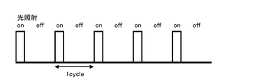
- pulse light means light having a short light irradiation period (irradiation time).
- the second light irradiation period (on) means light irradiation having a period (irradiation interval (off)) in which light is not irradiated.
- the pulsed light is emitted from a light source including a flash lamp such as a xenon flash lamp.
- a light source including a flash lamp such as a xenon flash lamp.
- the organic semiconductor material and / or the carbon-based semiconductor material constituting the semiconductor layer 4 is irradiated with pulsed light.
- one cycle (on + off) in FIG. 2 is repeated n times.
- the irradiation interval (off) of the pulsed light is preferably in the range of about 200 microseconds to about 99.98 milliseconds. If it is shorter than 200 microseconds, the adverse effect due to light deterioration and thermal deterioration becomes larger. Note that a light source operating at 10 Hz or higher can be used for the irradiation of the pulsed light.
- the pulsed light may be an electromagnetic wave having a wavelength range of 1 pm to 1 m, preferably an electromagnetic wave having a wavelength range of 10 nm to 1000 ⁇ m (from far ultraviolet to far infrared), more preferably 100 nm to 2000 nm.
- Electromagnetic waves in the wavelength range can be used. Examples of such electromagnetic waves include gamma rays, X-rays, ultraviolet rays, visible light, infrared rays, microwaves, radio waves on the longer wavelength side than microwaves, and the like.
- the wavelength range is preferably the ultraviolet to infrared range, more preferably the wavelength in the range of 100 nm to 2000 nm, among the wavelengths described above.
- the pulsed light irradiation step is not essential, it is preferably performed in an inert atmosphere (N 2 , Ar, He, etc.) or in a vacuum, and can be irradiated by heating. Therefore, it is preferable to irradiate near room temperature.
- Xenon's Sintron series As devices capable of performing such pulsed light irradiation, Xenon's Sintron series, NovaCentrix's PulseForge series, and the like are commercially available.
- the performance can be further improved by heat treatment.
- the heat treatment conditions are not essential, but are preferably in an inert atmosphere (N 2 , Ar, He, etc.) or in a vacuum, the temperature is 40 to 200 ° C., and the time is in the range of 5 minutes to 20 hours. It can be.
- the heat treatment conditions are in an efficient range in a normal production process, but the present invention is not necessarily limited to these conditions.
- the formation of the semiconductor layer can be easily formed by a wet process without using a dry process with low productivity and high cost. Production methods can be provided.
- the molecular order inside the device is improved despite the simple process, and the on-current of the field effect transistor can be amplified.
- the performance of the field effect transistor can be improved by heat treatment in an inert atmosphere (N 2 , Ar, He, etc.) or in vacuum.
- FIG. 3 is a schematic diagram of the structure of the field effect transistor device according to the example (the gate electrode is omitted).
- a semiconductor layer 9, a source electrode 10, and a drain electrode 11 are sequentially formed on a p-type or n-type doped silicon substrate 7 with an oxide film 8 having a thickness of 300 nm.
- Example 1 N-channel FET using fullerene derivative C 60 -mC12 (C 60 -fused N-methylpyrrolidine-meta-C12 phenyl)
- a p-type doped (doped species: boron) silicon substrate (20 mm ⁇ 20 mm ⁇ 525 ⁇ m t , resistivity: 0.02 ⁇ cm or less) with an oxide film (silicon oxide) having a thickness of 300 nm was ultrasonically cleaned with ethanol to obtain HMDS ( Surface treatment was performed by immersing in hexamethyldisilazane) for 1 hour. Thereafter, ultrasonic cleaning was performed with a chloroform solution.
- the transistor characteristics were measured in a vacuum of 10 ⁇ 5 to 10 ⁇ 6 Torr (1.33 ⁇ 10 ⁇ 3 to 1.33 ⁇ 10 ⁇ 4 Pa).
- Xenon Sinteron 2000 was used for pulsed light irradiation (irradiation conditions: 2070 J, pulse width 2000 microseconds, voltage 3000 V, irradiation distance 25.4 mm, single irradiation).
- the device irradiated with pulsed light showed carrier mobility of about 0.1 to 0.2 cm 2 / Vs, and the performance was improved over the device not irradiated with pulsed light (Comparative Example 1 described later).
- n-type doped (doped species: antimony) silicon substrate (20 mm ⁇ 20 mm ⁇ 525 ⁇ m t , resistivity: 0.02 ⁇ cm or less
- oxide film silicon oxide
- HMDS Hexamethyldisilazane
- Non-patent literature (Supporting of M. Lu, S. Nagamatsu, Y. Yoshida, M. Chikamatsu, R. Azumi, and K. Yase Chem. Lett., 2010, 39, 60. Information: http://www.jstage.jst.go.jp/article/cl/39/1/39_60/_applist) Prepared a 0.6 mass% solution of oligothiophene derivative (BHD6T) synthesized by the method described in chloroform The substrate was spin coated (2000 rpm / 60 seconds) to form a thin film. Thereafter, a transistor was manufactured under the same conditions as in Example 1. In the field effect transistor of this structure, the n-type doped silicon substrate functions as a gate electrode.
- BHD6T oligothiophene derivative
- Transistor characteristics were measured at room temperature in a nitrogen atmosphere.
- Xenon Sinteron 2000 was used for pulse light irradiation (irradiation conditions: 2070 J, pulse width 2000 microseconds, voltage 3000 V, irradiation distance 25.4 mm).
- the device irradiated with pulsed light showed carrier mobility of about 0.1 to 0.2 cm 2 / Vs, and the performance was improved over the device not irradiated with pulsed light (Comparative Example 2 described later). . This is considered to be due to the same reason as in the first embodiment.
- the same silicon substrate as the n-type doped silicon substrate with an oxide film (silicon oxide) having a thickness of 300 nm used in Example 2 was ultrasonically cleaned with ethanol, and immersed in HMDS (hexamethyldisilazane) for 2 hours. Processed. Thereafter, ultrasonic cleaning was performed with a chloroform solution.
- HMDS hexamethyldisilazane
- a 1% by mass chloroform solution of P3HT (Merck, trade name: Lisicon® SP001) was prepared and spin-coated on the substrate (1500 rpm / 60 seconds) to form a thin film.
- Gold was deposited on the thin film to a thickness of 30 nm using a 0.01 mm thick nickel mask having a predetermined opening pattern to form source and drain electrodes (electrode line width 100 ⁇ m).
- the n-type doped silicon substrate functions as a gate electrode.
- PulseForge 3300 manufactured by N0VACENTRIX was used (irradiation conditions: 189-509). mJ / cm 2 , pulse width 160-450 microseconds, voltage 180V).
- the same silicon substrate as the n-type doped silicon substrate with an oxide film (silicon oxide) having a thickness of 300 nm used in Example 2 was ultrasonically cleaned with ethanol, and immersed in HMDS (hexamethyldisilazane) for 2 hours. Processed. Thereafter, ultrasonic cleaning was performed with a chloroform solution.
- HMDS hexamethyldisilazane
- a 0.5 mass% chloroform solution of PQT-12 (American Dye Source (ADS), trade name: ADS12PQT) was prepared and spin-coated on the substrate (1500 rpm / 60 seconds) to form a thin film.
- Gold was deposited on the thin film to a thickness of 30 nm using a 0.01 mm thick nickel mask having a predetermined opening pattern to form source and drain electrodes (electrode line width 100 ⁇ m).
- the n-type doped silicon substrate functions as a gate electrode.
- PulseForge 3300 manufactured by N0VACENTRIX was used (irradiation conditions: 189-509). mJ / cm 2 , pulse width 160-450 microseconds, voltage 180V).
- a transistor was manufactured under the same conditions as in Example 1 except that pulsed light was not irradiated, and the characteristics were measured.
- the carrier mobility was about 0.05 cm 2 / Vs, which was a fraction of the value of the device irradiated with pulsed light.
- a transistor was manufactured under the same conditions as in Example 2 except that pulsed light was not irradiated, and the characteristics were measured.
- the carrier mobility was about 0.007 cm 2 / Vs, which was 1/10 or less of that of the device irradiated with pulsed light.
- a transistor was manufactured under the same conditions as in Example 3 except that no pulsed light was irradiated, and the characteristics were measured.
- the average carrier mobility was 3.3 ⁇ 10 ⁇ 3 cm 2 / Vs, which was lower than that of the device irradiated with pulsed light.
- a transistor was manufactured under the same conditions as in Example 4 except that no pulsed light was irradiated, and the characteristics were measured.
- the average carrier mobility was 8.5 ⁇ 10 ⁇ 5 cm 2 / Vs, which was lower than that of the device irradiated with pulsed light.
- the order of molecules inside the semiconductor material can be improved and the carrier mobility can be improved by a simple process of irradiating pulsed light.
- a field effect transistor with improved density can be manufactured at low cost.
- the semiconductor material activation method of the present invention can also be applied to the activation of semiconductor materials of other devices such as organic memories, organic solar cells, organic electroluminescent elements (organic EL, OLED), and is industrially useful.
Landscapes
- Physics & Mathematics (AREA)
- Electromagnetism (AREA)
- Optics & Photonics (AREA)
- Engineering & Computer Science (AREA)
- Manufacturing & Machinery (AREA)
- Thin Film Transistor (AREA)
Abstract
本発明は、半導体材料内部の分子の秩序性を改善し、キャリア移動度を向上することができる半導体材料活性化方法および電界効果トランジスタの製造方法を提供することを目的とする。 本発明は、有機半導体材料又は炭素系半導体材料が有機溶媒に溶解又は分散されたインキを使用し、基板上に印刷により膜又はパターンを形成して半導体層とし、更に半導体層に、1pm~1mの波長範囲の電磁波であり、照射時間が、約20マイクロ秒から約10ミリ秒の間であり、照射間隔が、約200マイクロ秒から約99.98ミリ秒の間であるパルス光を照射してキャリア移動度を向上させるものである。
Description
本発明は、有機半導体材料および/または炭素系半導体材料活性化方法の改良およびその方法を用いた電界効果トランジスタの製造方法に関する。
近年の電子機器には、電界効果トランジスタが多用され必要不可欠となっている。しかしながら、無機半導体材料を用いた電界効果トランジスタの製造には、多数の真空プロセス、不純物のドーピングプロセス等が必要であり、電界効果トランジスタの製造コストが高くなっていた。
一方、今日低価格で大量生産が必要とされている電子ペーパーや、RFIDタグ等の需要が高まっており、より低コスト、大量生産、短時間の回路製作により製造が可能である有機半導体が注目されている。有機半導体は、有機物の特性上、化合物半導体に比べて、スピンコート、印刷、インクジェット法等の低温下のウェットプロセスによる回路製作が可能であり、大面積、低コスト、簡易プロセスでの電界効果トランジスタの製造が期待されている(特許文献1、非特許文献1参照)。
"Hight-Resolution Inkjet Printing ofAll-Polymer Transistor Circuits" H. Sirringhaus et al., Science, Vol.290 (2000) 2123-2126
しかし、有機半導体材料を用いたウェットプロセスによる電界効果トランジスタは、単結晶化や真空蒸着法のようなドライプロセスを用いて製作された素子に比べ、素子内部での分子秩序性の低下、不純物の混入等が生じ、それがキャリア移動の障害となって電流密度が低下するという問題があった。
本発明は、上記従来の課題に鑑みなされたものであり、半導体材料内部の分子の秩序性を改善し、キャリア移動度を向上することができる半導体材料活性化方法および電界効果トランジスタの製造方法を提供することを目的とする。
上記目的を達成するために、請求項1に記載の半導体材料活性化方法の発明は、有機半導体材料および/または炭素系半導体材料のキャリア移動度を向上するための該材料の活性化方法であって、該材料にパルス光を照射することを特徴とする。
請求項2に記載の発明は、請求項1に記載の半導体材料活性化方法であって、前記パルス光が、1pm~1mの波長範囲の電磁波であることを特徴とする。
請求項3に記載の発明は、請求項1または請求項2に記載の半導体材料活性化方法であって、前記パルス光が、10nm~1000μmの波長範囲の電磁波であることを特徴とする。
請求項4に記載の発明は、請求項1から請求項3のいずれか一項に記載の半導体材料活性化方法であって、前記パルス光が、フラッシュランプを備える光源から照射されることを特徴とする。
請求項5に記載の発明は、請求項4に記載の半導体材料活性化方法であって、前記フラッシュランプが、キセノンフラッシュランプであることを特徴とする。
請求項6に記載の発明は、請求項1から請求項5のいずれか一項に記載の半導体材料活性化方法であって、前記パルス光の光源が繰り返しパルス光を照射できることを特徴とする。
請求項7に記載の発明は、請求項1から請求項6のいずれか一項に記載の半導体材料活性化方法であって、前記パルス光の照射時間が、約20マイクロ秒から約10ミリ秒の間であることを特徴とする。
請求項8に記載の発明は、請求項6に記載の半導体材料活性化方法であって、前記パルス光の照射間隔が、約200マイクロ秒から約99.98ミリ秒の間であることを特徴とする。
請求項9に記載の発明は、請求項8に記載の半導体材料活性化方法であって、前記パルス光の照射間隔が、10Hz以上で動作する光源により最長99.98ミリ秒であることを特徴とする。
請求項10に記載の発明は、請求項1から請求項9のいずれか一項に記載の半導体材料活性化方法であって、パルス光照射を室温で行うことを特徴とする。
請求項11に記載の発明は、請求項1から請求項10のいずれか一項に記載の半導体材料活性化方法であって、前記有機半導体材料がパイ共役系低分子または高分子化合物、及びそれらの誘導体からなる群から選択されるいずれかであり、前記炭素系半導体材料がフラーレン、カーボンナノチューブ及びそれらの誘導体からなる群から選択されるいずれかであることを特徴とする。
請求項12に記載の発明は、請求項1から請求項11のいずれか一項に記載の半導体材料活性化方法であって、前記有機半導体材料がオリゴチオフェン、ポリチオフェン及びそれらの誘導体からなる群から選択されるいずれかであり、前記炭素系半導体材料がフラーレン及びそれらの誘導体からなる群から選択されるいずれかであることを特徴とする。
請求項13に記載の発明は、請求項1から請求項12のいずれか一項に記載の半導体材料活性化方法であって、前記有機半導体材料が有機溶媒に溶解または分散されたインキを使用して基板上に印刷により膜またはパターンを形成した後に、前記パルス光を照射すること特徴とする。
請求項14に記載の発明は、請求項13に記載の半導体材料活性化方法であって、前記基板が、ポリエチレンテレフタレート、ポリエチレンナフタレート、ポリイミドまたはポリカーボネートを含む樹脂フィルム、熱硬化または熱可塑性樹脂成型体、アルミナ、シリカまたはガラスセラミックスを含むセラミックス成型体、ガラス繊維または炭素繊維とフェノール樹脂、エポキシ樹脂、ポリイミドまたはBT(ビスマレイミドトリアジン)レジンで構成された繊維強化樹脂積層体、紙製品およびこれらの等価物からなる群から選択される材料で構成される基板であることを特徴とする。
請求項15に記載の発明は、請求項13または請求項14に記載の半導体材料活性化方法であって、前記印刷プロセスが、スクリーン印刷、インクジェット印刷、転写印刷、グラビア印刷、レーザー印刷、ゼログラフィー印刷、パッド印刷、スピンコート法、キャスト法、ディッピング法、スプレーコート法、ディスペンサー法、フォトリソグラフィー法およびこれらの組合せからなる群から選択されることを特徴とする。
請求項16に記載の電界効果トランジスタの製造方法の発明は、請求項1から請求項15のいずれか一項に記載の半導体材料活性化方法により有機半導体材料および/または炭素系半導体材料を活性化させる工程を有することを特徴とする。
本発明によれば、パルス光を照射することにより電界効果トランジスタのキャリア移動度及び電流密度を向上させることができる。
以下、本発明を実施するための形態(以下、実施形態という)を説明する。
本発明者らは、上記目的を達成すべく鋭意研究を重ねた結果、パルス光照射を用いて、電界効果トランジスタの材料である有機半導体材料および/または炭素系半導体材料のキャリア移動度を向上させ、電流密度を向上できるという知見を得て、本発明を完成した。
図1(a)~(d)には、一般的な電界効果トランジスタ素子の構造が示される。ただし、本発明はこの構造に限定されるものではなく、他のゲート電極、ゲート絶縁膜層、半導体層の層構造を有するものであっても電界効果トランジスタであれば、何れにも本発明を適用できる。
図1(a)は、基板1の上にゲート電極2、ゲート絶縁膜3、半導体層4、ソース電極5、ドレイン電極6が順次形成された構造である。また、図1(b)は、基板1の上にゲート電極2、ゲート絶縁膜3、ソース電極5、ドレイン電極6、半導体層4が順次形成された構造である。また、図1(c)は、基板1の上に半導体層4、ソース電極5、ドレイン電極6、ゲート絶縁膜3、ゲート電極2が順次形成された構造である。また、図1(d)は、基板1の上にソース電極5、ドレイン電極6、半導体層4、ゲート絶縁膜3、ゲート電極2が順次形成された構造である。
上記半導体層4は、有機半導体材料ないし炭素系半導体材料で形成される。これらの材料としては、各種公知のウェットプロセスに適用可能な材料を使用でき、例えば有機半導体材料としては微結晶のペンタセン、オリゴチオフェン、ポリチオフェン、フルオレン-ビチオフェン共重合体等のパイ共役系低分子または高分子化合物、およびそれらの誘導体、炭素系半導体材料としてはフラーレン、カーボンナノチューブ及びそれらの誘導体等を用いることができるが、本実施形態の半導体層4に用いられる有機半導体材料、炭素系半導体材料は、これらに制限されるものではない。なお、上記有機半導体材料のうち、特にオリゴチオフェン、ポリチオフェン及びそれらの誘導体が好適であり、上記炭素系半導体材料のうち、特にフラーレン及びそれらの誘導体が好適である。これらの化合物は有機溶媒に溶解または分散されたインキを使用したウェットプロセスにより基板上に印刷すると結晶性の薄膜となる傾向が高いため、製膜後の後処理により結晶化度を向上させることによって、より高性能なデバイスとすることが可能だからである。なお、オリゴチオフェンとポリチオフェンとは分子量において相違するが、両者に明確な分子量の境界値はない。本明細書においては10量体未満のものを「オリゴチオフェン」、10量体以上のものを「ポリチオフェン」と呼ぶ。
上記半導体層4を形成する各種公知のウェットプロセスでは、上記有機半導体材料および/または炭素系半導体材料が有機溶媒に溶解または分散されたインキを使用し、基板上に印刷により膜またはパターンを形成することにより半導体層4とする。このようなウェットプロセスとしては、例えばスクリーン印刷、インクジェット印刷、転写印刷、グラビア印刷、レーザー印刷、ゼログラフィー印刷、パッド印刷、スピンコート法、キャスト法、ディッピング法、スプレーコート法、ディスペンサー法、フォトリソグラフィー法等が挙げられ、その際、有機溶媒としてジクロロメタン、クロロホルム、二硫化炭素、アセトニトリル、ジメチルホルムアミド、ベンゼン、トルエン、キシレン、クロロベンゼン、ジクロロベンゼン、トリクロロベンゼン等を用いることができる。また、上記ウェットプロセスは、適宜組み合わせて実施してもよい。
なお、上記各ウェットプロセスは代表的な例を述べているものであって、半導体層4の形成方法は、これらに限定されるものではない。
上記基板1は、ポリエチレンテレフタレート、ポリエチレンナフタレート、ポリイミドまたはポリカーボネートを含む樹脂フィルム、熱硬化または熱可塑性樹脂成型体、アルミナ、シリカまたはガラスセラミックス(結晶化ガラス)を含むセラミックス成型体、ガラス繊維または炭素繊維とフェノール樹脂、エポキシ樹脂、ポリイミドまたはBT(ビスマレイミドトリアジン)レジンで構成された繊維強化樹脂積層体、紙製品およびこれらの等価物からなる群から選択される材料で構成することができるが、これらに限られるものではない。
上記ゲート絶縁膜3は、絶縁性を有する材料であれば特に制限はなく、例えば酸化シリコン、窒化シリコン、酸化チタン、酸化アルミニウム等の無機物やPVA(ポリビニルアルコール)、PMMA(ポリメチルメタクリレート)、PVP(ポリビニルフェノール)、BCB(ジビニルテトラメチルジシロキサン ビスベンゾシクロブテン)等の有機物を用いることができるが、絶縁膜材も同様にこれらに制限されるものではない。
上記ゲート電極2の材料としては、pまたはn型ドープシリコン、インジウム、ITOやドーピングにより導電性を示すポリチオフェン、ポリアニリン等の高分子や金、銀、白金、クロム等の金属を用いることができるが、これらに限定されるものではない。
ソース電極5及びドレイン電極6は、真空蒸着、スパッタ、CVD(化学気相成長)等の気相成長法やインクジェットその他の印刷法により形成してもよい。
ここでソース電極5、ドレイン電極6の導電材料としてはクロム、アルミニウム、インジウム、貴金属類(Au、Ag、Cu、Pt)、アルカリ金属(Li、Na、K、Rb、Cs)、アルカリ土類金属(Mg、Ca、Sr、Ba)等の金属材料あるいはカーボン等の微粉体、ならびにナノ粒子や有機Ag化合物等の導電材を含有する各種導電性ペースト等の公知の材料を用いることができる。電極材もこれらに限定されるものではない。
本実施形態では、上記ウェットプロセスにより有機半導体材料および/または炭素系半導体材料で半導体層4を形成した後、さらにこれにパルス光を照射してキャリア移動度を向上させる。本明細書中において「パルス光」とは、光照射期間(照射時間)が短時間の光であり、光照射を複数回繰り返す場合は図2に示すように、第一の光照射期間(on)と第二の光照射期間(on)との間に光が照射されない期間(照射間隔(off))を有する光照射を意味する。図2ではパルス光の光強度が一定であるように示しているが、1回の光照射期間(on)内で光強度が変化してもよい。上記パルス光は、キセノンフラッシュランプ等のフラッシュランプを備える光源から照射される。このような光源を使用して、半導体層4を構成する有機半導体材料および/または炭素系半導体材料にパルス光を照射する。n回繰り返し照射する場合は、図2における1サイクル(on+off)をn回反復する。なお、繰り返し照射する場合には、次パルス光照射を行う際に、基材を室温付近まで冷却できるようにするため基材側から冷却することが好ましい。
パルス光の1回の照射時間(on)としては、約20マイクロ秒から約10ミリ秒の範囲が好ましい。20マイクロ秒よりも短いと性能向上の効果が低く、10ミリ秒よりも長いと光劣化、熱劣化による悪影響のほうが大きくなり好ましくない。パルス光の照射は単発で実施しても効果はあるが、上記の通り繰り返し実施することもできる。その際のパルス光の照射間隔(off)は、約200マイクロ秒から約99.98ミリ秒の範囲が好ましい。200マイクロ秒より短いと光劣化、熱劣化による悪影響のほうが大きくなり、99.98ミリ秒よりも長いと性能向上の効果が低くなり好ましくない。なお、上記パルス光の照射には、10Hz以上で動作する光源を使用することができる。
また、上記パルス光としては、1pm~1mの波長範囲の電磁波を使用することができ、好ましくは10nm~1000μmの波長範囲の電磁波(遠紫外から遠赤外まで)、さらに好ましくは100nm~2000nmの波長範囲の電磁波を使用することができる。このような電磁波の例としては、ガンマ線、X線、紫外線、可視光、赤外線、マイクロ波、マイクロ波より長波長側の電波等が挙げられる。なお、熱エネルギーへの変換を考えた場合には、あまりに波長が短い場合には、半導体材料自体へのダメージが大きく好ましくない。また、波長が長すぎる場合には効率的に吸収して発熱することが出来ないので好ましくない。従って、波長の範囲としては、前述の波長の中でも特に紫外から赤外の範囲が好ましく、より好ましくは100nm~2000nmの範囲の波長である。
上記パルス光の照射工程は、必須ではないものの不活性雰囲気下(N2、Ar、He等)または真空中で実施することが望ましく、加熱して照射することもできるが、照射前に熱変性を受けるおそれもあるので、室温付近で照射することが好ましい。
このようなパルス光照射を行える装置としては、Xenon社のSintronシリーズ、NovaCentrix社のPulseForgeシリーズ等が市販されている。
また、パルス照射の後、更に加熱処理によって性能を向上させることが出来る。加熱処理の条件としては、必須ではないものの、不活性雰囲気下(N2、Ar、He等)または真空中が望ましく、温度は40~200℃の温度で、時間は5分~20時間の範囲とすることができる。この加熱処理条件は、通常の生産工程で効率的な範囲のものであるが、本発明は必ずしもこの条件に制限されるものではない。
以上に述べた実施形態によれば、半導体層の形成に生産性の低下、高コストを伴うドライプロセスを用いず、ウェットプロセスにより簡易的に形成できるので、高性能の電界効果トランジスタの低コストでの生産法を提供することができる。また、簡易プロセスでありながら素子内部の分子秩序が改善され電界効果トランジスタのオン電流の増幅を行うことができる。さらに、不活性雰囲気下(N2、Ar、He等)又は真空中で加熱処理することにより電界効果トランジスタの性能を向上させることができる。
以下、本発明の実施例を具体的に説明する。なお、以下の実施例及び比較例は、本発明の理解を容易にするためのものであり、本発明はこれらの実施例に制限されるものではない。
図3は、実施例にかかる電界効果トランジスタ素子の構造の概要図である(ゲート電極は省略している)。厚さ300nmの酸化膜8のついたpまたはn型ドープシリコン基板7に半導体層9、ソース電極10、ドレイン電極11を順次形成した構造である。
実施例1
フラーレン誘導体C60-mC12(C60-fused N-methylpyrrolidine-meta-C12 phenyl)を用いたNチャネルFET
フラーレン誘導体C60-mC12(C60-fused N-methylpyrrolidine-meta-C12 phenyl)を用いたNチャネルFET
厚さ300nmの酸化膜(酸化シリコン)がついたp型ドープ(ドープ種:ボロン)シリコン基板(20mm×20mm×525μmt、抵抗率:0.02Ωcm以下)をエタノールで超音波洗浄し、HMDS(ヘキサメチルジシラザン)に1時間浸して表面処理を行った。その後、クロロホルム溶液で超音波洗浄した。
非特許文献(”Studies on Structures and Properties of Long Alkyl Chain-linked C60 Cast Films” 近松真之博士学位論文(2001年 東京都立大学))記載の方法により合成したC60-mC12(上記論文中ではm-C12と表記)のクロロホルム1.0質量%溶液を調製し、上記基板にスピンコートし(2000rpm/60秒)、薄膜を形成した。薄膜の上に所定の開口パターンを有する厚さ0.01mmのニッケル製マスクを用いてチャネル長20μm、チャネル幅5mm、厚さ30nmとなるように金を蒸着してソース、ドレイン電極(ともに5mm×1mm)を形成した。本構造の電界効果トランジスタではp型ドープシリコン基板がゲート電極として機能する。
トランジスタ特性の測定は、10-5~10-6Torr(1.33×10⁻³~1.33×10⁻⁴Pa)の真空中で行った。パルス光照射にはXenon社製Sinteron2000を用いた(照射条件:2070J、パルス幅2000マイクロ秒、電圧3000V、照射距離25.4mm、単発照射)。
トランジスタ特性を測定したところ、パルス光照射したデバイスは0.1~0.2cm2/Vs程度のキャリア移動度を示し、パルス光照射していないデバイス(後述の比較例1)より性能が向上した。これは、パルス光照射により半導体材料であるC60-mC12の薄膜が局所的に加熱されることにより薄膜中に含まれる溶媒、酸素、水等の残留物の除去や結晶性の向上が図られたためと考えられる。
実施例2
オリゴチオフェン誘導体(α,ω-bis(2-hexyldecyl)-sexithiophene(BHD6T))を用いたPチャネルFET
オリゴチオフェン誘導体(α,ω-bis(2-hexyldecyl)-sexithiophene(BHD6T))を用いたPチャネルFET
厚さ300nmの酸化膜(酸化シリコン)がついたn型ドープ(ドープ種:アンチモン)シリコン基板(20mm×20mm×525μmt、抵抗率:0.02Ωcm以下)をエタノールで超音波洗浄し、HMDS(ヘキサメチルジシラザン)に1時間浸し、表面処理を行った。その後、クロロホルム溶液で超音波洗浄した。
非特許文献(M. Lu, S. Nagamatsu, Y. Yoshida, M. Chikamatsu, R. Azumi, and K. Yase Chem.Lett., 2010, 39, 60.のSupporting
Information:http://www.jstage.jst.go.jp/article/cl/39/1/39_60/_applist)記載の方法により合成したオリゴチオフェン誘導体(BHD6T)のクロロホルム0.6質量%溶液を調製し、上記基板にスピンコートし(2000rpm/60秒)、薄膜を形成した。その後、実施例1と同様の条件でトランジスタを作製した。本構造の電界効果トランジスタではn型ドープシリコン基板がゲート電極として機能する。
Information:http://www.jstage.jst.go.jp/article/cl/39/1/39_60/_applist)記載の方法により合成したオリゴチオフェン誘導体(BHD6T)のクロロホルム0.6質量%溶液を調製し、上記基板にスピンコートし(2000rpm/60秒)、薄膜を形成した。その後、実施例1と同様の条件でトランジスタを作製した。本構造の電界効果トランジスタではn型ドープシリコン基板がゲート電極として機能する。
トランジスタ特性の測定は、窒素雰囲気中、室温で行った。パルス光照射にはXenon社製Sinteron2000を用いた(照射条件:2070J、パルス幅2000マイクロ秒、電圧3000V、照射距離25.4mm)。
トランジスタ特性を測定したところ、パルス光照射したデバイスは0.1~0.2cm2/Vs程度のキャリア移動度を示し、パルス光照射していないデバイス(後述の比較例2)より性能が向上した。これは実施例1と同様の理由によるものと考えられる。
実施例3
ポリチオフェン誘導体(Poly(3-hexylthiophene)(P3HT))を用いたPチャネルFET
ポリチオフェン誘導体(Poly(3-hexylthiophene)(P3HT))を用いたPチャネルFET
実施例2で用いた厚さ300nmの酸化膜(酸化シリコン)がついたn型ドープシリコン基板と同一のシリコン基板をエタノールで超音波洗浄し、HMDS(ヘキサメチルジシラザン)に2時間浸し、表面処理を行った。その後、クロロホルム溶液で超音波洗浄した。
P3HT(Merck社製、商品名:Lisicon SP001)のクロロホルム1質量%溶液を調製し、上記基板にスピンコートし(1500rpm/60秒)、薄膜を形成した。薄膜の上に所定の開口パターンを有する厚さ0.01mmのニッケル製マスクを用いて厚さ30nmとなるように金を蒸着してソース、ドレイン電極(電極の線幅100μm)を形成した。チャネル長/チャネル幅は、40μm/1mm、80μm/2mm、120μm/3mm、160μm/4mmの4種類である。本構造の電界効果トランジスタではn型ドープシリコン基板がゲート電極として機能する。
トランジスタ特性の測定は、窒素雰囲気中、室温で行った。パルス光照射にはN0VACENTRIX社製PulseForge3300を用いた(照射条件:189-509
mJ/cm2、パルス幅160-450マイクロ秒、電圧180V)。
mJ/cm2、パルス幅160-450マイクロ秒、電圧180V)。
トランジスタ特性を測定したところ、照射条件189mJ/cm2(パルス幅160マイクロ秒、電圧180V)で平均7.6×10-3cm2/Vs、照射条件348mJ/cm2(パルス幅300マイクロ秒、電圧180V)で平均6.5×10-3cm2/Vs、照射条件509mJ/cm2(パルス幅450マイクロ秒、電圧180V)で平均4.3×10-3cm2/Vsのャリア移動度を示し、パルス光照射していないデバイス(後述の比較例3)より性能が向上した。これは実施例1と同様の理由によるものと考えられる。
実施例4
ポリチオフェン誘導体(Poly(3,3’’’-didodecylquaterthiophene)(PQT-12))を用いたPチャネルFET
ポリチオフェン誘導体(Poly(3,3’’’-didodecylquaterthiophene)(PQT-12))を用いたPチャネルFET
実施例2で用いた厚さ300nmの酸化膜(酸化シリコン)がついたn型ドープシリコン基板と同一のシリコン基板をエタノールで超音波洗浄し、HMDS(ヘキサメチルジシラザン)に2時間浸し、表面処理を行った。その後、クロロホルム溶液で超音波洗浄した。
PQT-12(American Dye Source(ADS)社製、商品名:ADS12PQT)のクロロホルム0.5質量%溶液を調製し、上記基板にスピンコートし(1500rpm/60秒)、薄膜を形成した。薄膜の上に所定の開口パターンを有する厚さ0.01mmのニッケル製マスクを用いて厚さ30nmとなるように金を蒸着してソース、ドレイン電極(電極の線幅100μm)を形成した。チャネル長/チャネル幅は、40μm/1mm、80μm/2mm、120μm/3mm、160μm/4mmの4種類である。本構造の電界効果トランジスタではn型ドープシリコン基板がゲート電極として機能する。
トランジスタ特性の測定環境は、窒素雰囲気中、室温で行った。パルス光照射にはN0VACENTRIX社製PulseForge3300を用いた(照射条件:189-509
mJ/cm2、パルス幅160-450マイクロ秒、電圧180V)。
mJ/cm2、パルス幅160-450マイクロ秒、電圧180V)。
トランジスタ特性を測定したところ、照射条件189mJ/cm2(パルス幅160マイクロ秒、電圧180V)で平均1.1×10-4cm2/Vs、照射条件509mJ/cm2(パルス幅450マイクロ秒、電圧180V)で平均1.1×10-4cm2/Vsのャリア移動度を示し、パルス光照射していないデバイス(後述の比較例4)より性能が向上した。これは実施例1と同様の理由によるものと考えられる。
比較例1
フラーレン誘導体C60-mC12(C60-fused N-methylpyrrolidine-meta-C12 phenyl)を用いたNチャネルFET
フラーレン誘導体C60-mC12(C60-fused N-methylpyrrolidine-meta-C12 phenyl)を用いたNチャネルFET
パルス光を照射しない以外は実施例1と同条件でトランジスタを作製し、特性を測定した。0.05cm2/Vs程度のキャリア移動度を示し、パルス光照射したデバイスの数分の1の値であった。
比較例2
オリゴチオフェン誘導体(α,ω-bis(2-hexyldecyl)-sexithiophene(BHD6T))を用いたPチャネルFET
オリゴチオフェン誘導体(α,ω-bis(2-hexyldecyl)-sexithiophene(BHD6T))を用いたPチャネルFET
パルス光を照射しない以外は実施例2と同条件でトランジスタを作製し、特性を測定した。0.007cm2/Vs程度のキャリア移動度を示し、パルス光照射したデバイスの10分の1以下の値であった。
比較例3
ポリチオフェン誘導体(Poly(3-hexylthiophene)(P3HT))を用いたPチャネルFET
ポリチオフェン誘導体(Poly(3-hexylthiophene)(P3HT))を用いたPチャネルFET
パルス光を照射しない以外は実施例3と同条件でトランジスタを作製し、特性を測定した。平均で3.3×10⁻³cm2/Vsのキャリア移動度を示し、パルス光照射したデバイスより低い値であった。
比較例4
ポリチオフェン誘導体(Poly(3,3’’’-didodecylquaterthiophene)(PQT-12))を用いたPチャネルFET
ポリチオフェン誘導体(Poly(3,3’’’-didodecylquaterthiophene)(PQT-12))を用いたPチャネルFET
パルス光を照射しない以外は実施例4と同条件でトランジスタを作製し、特性を測定した。平均で8.5×10⁻⁵cm2/Vsのキャリア移動度を示し、パルス光照射したデバイスより低い値であった。
本発明の半導体材料活性化方法によれば、パルス光を照射するという簡単な処理により半導体材料内部の分子の秩序性を改善し、キャリア移動度を向上させることができるので、キャリア移動度及び電流密度の向上した電界効果トランジスタを低コストで製造することができる。また、本発明の半導体材料活性化方法は有機メモリ、有機太陽電池、有機電界発光素子(有機EL、OLED)等他のデバイスの半導体材料の活性化にも適用でき、工業的に有用である。
1 基板、2 ゲート電極、3 ゲート絶縁膜、4 半導体層、5 ソース電極、6 ドレイン電極、7 pまたはn型ドープシリコン基板、8 酸化膜、9 半導体層、10 ソース電極、11 ドレイン電極。
Claims (16)
- 有機半導体材料および/または炭素系半導体材料のキャリア移動度を向上するための該材料の活性化方法であって、該材料にパルス光を照射することを特徴とする半導体材料活性化方法。
- 前記パルス光が、1pm~1mの波長範囲の電磁波であることを特徴とする請求項1に記載の半導体材料活性化方法。
- 前記パルス光が、10nm~1000μmの波長範囲の電磁波であることを特徴とする請求項1または請求項2に記載の半導体材料活性化方法。
- 前記パルス光が、フラッシュランプを備える光源から照射されることを特徴とする請求項1から請求項3のいずれか一項に記載の半導体材料活性化方法。
- 前記フラッシュランプが、キセノンフラッシュランプであることを特徴とする請求項4に記載の半導体材料活性化方法。
- 前記パルス光の光源が繰り返しパルス光を照射できることを特徴とする請求項1から請求項5のいずれか一項に記載の半導体材料活性化方法。
- 前記パルス光の照射時間が、約20マイクロ秒から約10ミリ秒の間であることを特徴とする請求項1から請求項6のいずれか一項に記載の半導体材料活性化方法。
- 前記パルス光の照射間隔が、約200マイクロ秒から約99.98ミリ秒の間であることを特徴とする請求項6に記載の半導体材料活性化方法。
- 前記パルス光の照射間隔が、10Hz以上で動作する光源により最長99.98ミリ秒であることを特徴とする請求項8に記載の半導体材料活性化方法。
- パルス光照射を室温で行うことを特徴とする請求項1から請求項9のいずれか一項に記載の半導体材料活性化方法。
- 前記有機半導体材料がパイ共役系低分子または高分子化合物、及びそれらの誘導体からなる群から選択されるいずれかであり、前記炭素系半導体材料がフラーレン、カーボンナノチューブ及びそれらの誘導体からなる群から選択されるいずれかであることを特徴とする請求項1から請求項10のいずれか一項に記載の半導体材料活性化方法。
- 前記有機半導体材料がオリゴチオフェン、ポリチオフェン及びそれらの誘導体からなる群から選択されるいずれかであり、前記炭素系半導体材料がフラーレン及びそれらの誘導体からなる群から選択されるいずれかであることを特徴とする請求項1から請求項11のいずれか一項に記載の半導体材料活性化方法。
- 前記有機半導体材料が有機溶媒に溶解または分散されたインキを使用して基板上に印刷により膜またはパターンを形成した後に、前記パルス光を照射すること特徴とする請求項1から請求項12のいずれか一項に記載の半導体材料活性化方法。
- 前記基板が、ポリエチレンテレフタレート、ポリエチレンナフタレート、ポリイミドまたはポリカーボネートを含む樹脂フィルム、熱硬化または熱可塑性樹脂成型体、アルミナ、シリカまたはガラスセラミックスを含むセラミックス成型体、ガラス繊維または炭素繊維とフェノール樹脂、エポキシ樹脂、ポリイミドまたはBT(ビスマレイミドトリアジン)レジンで構成された繊維強化樹脂積層体、紙製品およびこれらの等価物からなる群から選択される材料で構成される基板であることを特徴とする請求項13に記載の半導体材料活性化方法。
- 前記印刷プロセスが、スクリーン印刷、インクジェット印刷、転写印刷、グラビア印刷、レーザー印刷、ゼログラフィー印刷、パッド印刷、スピンコート法、キャスト法、ディッピング法、スプレーコート法、ディスペンサー法、フォトリソグラフィー法およびこれらの組合せからなる群から選択されることを特徴とする請求項13または請求項14に記載の半導体材料活性化方法。
- 請求項1から請求項15のいずれか一項に記載の半導体材料活性化方法により有機半導体材料および/または炭素系半導体材料を活性化させる工程を有することを特徴とする電界効果トランジスタの製造方法。
Applications Claiming Priority (2)
| Application Number | Priority Date | Filing Date | Title |
|---|---|---|---|
| JP2011-086982 | 2011-04-11 | ||
| JP2011086982 | 2011-04-11 |
Publications (1)
| Publication Number | Publication Date |
|---|---|
| WO2012141116A1 true WO2012141116A1 (ja) | 2012-10-18 |
Family
ID=47009289
Family Applications (1)
| Application Number | Title | Priority Date | Filing Date |
|---|---|---|---|
| PCT/JP2012/059632 Ceased WO2012141116A1 (ja) | 2011-04-11 | 2012-04-09 | 有機半導体材料活性化方法 |
Country Status (2)
| Country | Link |
|---|---|
| TW (1) | TW201308437A (ja) |
| WO (1) | WO2012141116A1 (ja) |
Citations (2)
| Publication number | Priority date | Publication date | Assignee | Title |
|---|---|---|---|---|
| JP2004247716A (ja) * | 2003-01-23 | 2004-09-02 | Mitsubishi Chemicals Corp | 積層体の製造方法 |
| JP2010045327A (ja) * | 2008-08-11 | 2010-02-25 | Korea Electronics Telecommun | 有機薄膜の局所的結晶化方法及びこれを利用した有機薄膜トランジスタの製造方法 |
-
2012
- 2012-04-09 WO PCT/JP2012/059632 patent/WO2012141116A1/ja not_active Ceased
- 2012-04-11 TW TW101112775A patent/TW201308437A/zh unknown
Patent Citations (2)
| Publication number | Priority date | Publication date | Assignee | Title |
|---|---|---|---|---|
| JP2004247716A (ja) * | 2003-01-23 | 2004-09-02 | Mitsubishi Chemicals Corp | 積層体の製造方法 |
| JP2010045327A (ja) * | 2008-08-11 | 2010-02-25 | Korea Electronics Telecommun | 有機薄膜の局所的結晶化方法及びこれを利用した有機薄膜トランジスタの製造方法 |
Also Published As
| Publication number | Publication date |
|---|---|
| TW201308437A (zh) | 2013-02-16 |
Similar Documents
| Publication | Publication Date | Title |
|---|---|---|
| Yang et al. | Insight into high-performance conjugated polymers for organic field-effect transistors | |
| Khim et al. | High performance and stable N-channel organic field-effect transistors by patterned solvent-vapor annealing | |
| Jung et al. | A TIPS-TPDO-tetraCN-based n-type organic field-effect transistor with a cross-linked PMMA polymer gate dielectric | |
| Baeg et al. | Controlled charge transport by polymer blend dielectrics in top-gate organic field-effect transistors for low-voltage-operating complementary circuits | |
| Baeg et al. | Improved performance uniformity of inkjet printed n-channel organic field-effect transistors and complementary inverters | |
| US9246008B2 (en) | Thin-film device, method of manufacturing the same, and method of manufacturing image display apparatus | |
| TW201503266A (zh) | 有機半導體薄膜的製作方法 | |
| Dey et al. | High-performance n-channel organic thin-film transistor based on naphthalene diimide | |
| KR20100045438A (ko) | N,n'-비스(1,1-디하이드로퍼플루오로-c3-c5-알킬)퍼릴렌-3,4:9,10-테트라카르복실산 디이미드의 용도 | |
| CN106459748B (zh) | N-氟烷基取代的二溴萘二酰亚胺及其用作半导体的用途 | |
| Liu et al. | Experimental study and statistical analysis of solution-shearing processed organic transistors based on an asymmetric small-molecule semiconductor | |
| KR101172187B1 (ko) | 스프레이 방식을 이용한 박막트랜지스터 및 전자회로를 제조하는 방법 | |
| Nakayama et al. | Characterization and field-effect transistor performance of printed pentacene films prepared by photoconversion of a soluble precursor | |
| Takimiya et al. | Molecular Modification of 2, 6-Diphenylbenzo [1, 2-b: 4, 5-b′] dichalcogenophenes by Introduction of Strong Electron-withdrawing Groups: Conversion from p-to n-Channel OFET Materials | |
| Park et al. | Efficient solvent-assisted post-treatment for molecular rearrangement of sprayed polymer field-effect transistors | |
| Park et al. | High-performance n-type organic field-effect transistors fabricated by ink-jet printing using a C60 derivative | |
| JP6592863B2 (ja) | 有機化合物及びその用途 | |
| JP6572473B2 (ja) | 有機化合物及びその用途 | |
| WO2012141116A1 (ja) | 有機半導体材料活性化方法 | |
| WO2014047647A1 (en) | Organic thin film transistors and methods of making the same | |
| Kim et al. | Thermal Gradient During Vacuum-Deposition Dramatically Enhances Charge Transport in Organic Semiconductors: Toward High-Performance N-Type Organic Field-Effect Transistors | |
| JP5469358B2 (ja) | 有機トランジスタ | |
| Ito et al. | High-performance solution-processed organic transistors with electroless-plated electrodes | |
| Mukherjee et al. | One-step fabrication of ordered organic crystalline array for novel optoelectronic applications | |
| Ribierre et al. | Influence of gate dielectric on the ambipolar characteristics of solution-processed organic field-effect transistors |
Legal Events
| Date | Code | Title | Description |
|---|---|---|---|
| 121 | Ep: the epo has been informed by wipo that ep was designated in this application |
Ref document number: 12771630 Country of ref document: EP Kind code of ref document: A1 |
|
| NENP | Non-entry into the national phase |
Ref country code: DE |
|
| 122 | Ep: pct application non-entry in european phase |
Ref document number: 12771630 Country of ref document: EP Kind code of ref document: A1 |
|
| NENP | Non-entry into the national phase |
Ref country code: JP |