WO2012137583A1 - Optical element, color wheel, illumination device, and projection display device - Google Patents
Optical element, color wheel, illumination device, and projection display device Download PDFInfo
- Publication number
- WO2012137583A1 WO2012137583A1 PCT/JP2012/056729 JP2012056729W WO2012137583A1 WO 2012137583 A1 WO2012137583 A1 WO 2012137583A1 JP 2012056729 W JP2012056729 W JP 2012056729W WO 2012137583 A1 WO2012137583 A1 WO 2012137583A1
- Authority
- WO
- WIPO (PCT)
- Prior art keywords
- light
- layer
- optical element
- phosphor layer
- dielectric constant
- Prior art date
Links
Images


Classifications
-
- G—PHYSICS
- G02—OPTICS
- G02B—OPTICAL ELEMENTS, SYSTEMS OR APPARATUS
- G02B5/00—Optical elements other than lenses
- G02B5/18—Diffraction gratings
-
- G—PHYSICS
- G02—OPTICS
- G02B—OPTICAL ELEMENTS, SYSTEMS OR APPARATUS
- G02B1/00—Optical elements characterised by the material of which they are made; Optical coatings for optical elements
- G02B1/10—Optical coatings produced by application to, or surface treatment of, optical elements
- G02B1/11—Anti-reflection coatings
- G02B1/118—Anti-reflection coatings having sub-optical wavelength surface structures designed to provide an enhanced transmittance, e.g. moth-eye structures
-
- G—PHYSICS
- G02—OPTICS
- G02B—OPTICAL ELEMENTS, SYSTEMS OR APPARATUS
- G02B26/00—Optical devices or arrangements for the control of light using movable or deformable optical elements
- G02B26/007—Optical devices or arrangements for the control of light using movable or deformable optical elements the movable or deformable optical element controlling the colour, i.e. a spectral characteristic, of the light
- G02B26/008—Optical devices or arrangements for the control of light using movable or deformable optical elements the movable or deformable optical element controlling the colour, i.e. a spectral characteristic, of the light in the form of devices for effecting sequential colour changes, e.g. colour wheels
-
- G—PHYSICS
- G03—PHOTOGRAPHY; CINEMATOGRAPHY; ANALOGOUS TECHNIQUES USING WAVES OTHER THAN OPTICAL WAVES; ELECTROGRAPHY; HOLOGRAPHY
- G03B—APPARATUS OR ARRANGEMENTS FOR TAKING PHOTOGRAPHS OR FOR PROJECTING OR VIEWING THEM; APPARATUS OR ARRANGEMENTS EMPLOYING ANALOGOUS TECHNIQUES USING WAVES OTHER THAN OPTICAL WAVES; ACCESSORIES THEREFOR
- G03B21/00—Projectors or projection-type viewers; Accessories therefor
- G03B21/14—Details
- G03B21/20—Lamp housings
- G03B21/2006—Lamp housings characterised by the light source
- G03B21/2033—LED or laser light sources
- G03B21/204—LED or laser light sources using secondary light emission, e.g. luminescence or fluorescence
-
- H—ELECTRICITY
- H04—ELECTRIC COMMUNICATION TECHNIQUE
- H04N—PICTORIAL COMMUNICATION, e.g. TELEVISION
- H04N9/00—Details of colour television systems
- H04N9/12—Picture reproducers
- H04N9/31—Projection devices for colour picture display, e.g. using electronic spatial light modulators [ESLM]
- H04N9/3102—Projection devices for colour picture display, e.g. using electronic spatial light modulators [ESLM] using two-dimensional electronic spatial light modulators
- H04N9/3111—Projection devices for colour picture display, e.g. using electronic spatial light modulators [ESLM] using two-dimensional electronic spatial light modulators for displaying the colours sequentially, e.g. by using sequentially activated light sources
- H04N9/3114—Projection devices for colour picture display, e.g. using electronic spatial light modulators [ESLM] using two-dimensional electronic spatial light modulators for displaying the colours sequentially, e.g. by using sequentially activated light sources by using a sequential colour filter producing one colour at a time
Definitions
- An optical element includes a metal layer, a dielectric layer laminated on the metal layer, and a phosphor layer that is laminated on the dielectric layer and emits fluorescence by incident light.
- a diffraction grating is formed at the interface between the layer and the phosphor layer, and the dielectric constant of the dielectric layer is higher than 2.25.
- each layer is very thin and the difference in thickness between the layers is large, so that it is difficult to illustrate each layer with an accurate scale and ratio.
- the layers are not schematically drawn but are shown schematically.
- a plane parallel to the substrate 11 is defined as an XY plane, and a direction orthogonal to the XY plane is defined as a Z direction.
- Re [] represents taking a real part in [].
- the interaction distance which is the distance from the exciton to the metal layer 12
- the coupling efficiency between the exciton and the surface plasmon becomes smaller.
- the distance from the surface of the phosphor layer 14 opposite to the high dielectric constant layer 13 to the metal layer 12 is an effective interaction distance that is an interaction distance at which the surface plasmon intensity is e-2 times the maximum value. You can do it.
- the effective interaction distance deff is an effective interaction distance that is an interaction distance at which the surface plasmon intensity is e-2 times the maximum value. You can do it.
- the effective interaction distance deff is
- the dielectric constant of the metal layer 12 since the dielectric constant of the metal layer 12 has an imaginary part, the surface plasmon is excited even if the real part of the effective dielectric constant of the input / output part exceeds the absolute value of the real part of the dielectric constant of the metal layer 12. However, if the difference between the absolute values of the real part of the effective dielectric constant of the incident / exit part and the real part of the dielectric constant of the metal layer 12 is large, the surface plasmon is not excited.
- 4 to 9 are diagrams showing an example of the phosphor layer 14, and shows a cross section of the optical element 1 cut along the YZ plane and an upper surface of the optical element 1 viewed from the + Z direction.
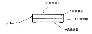
- FIG. 10 is a diagram showing another form of the optical element. 10, in addition to the optical element 1 shown in FIG. 1, the optical element 1 ′ includes a cooling layer 15 provided on the phosphor layer 14, and a cover 17 that covers the optical element 1 and the cooling layer 15. Also have.
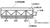
- FIG. 11 is a diagram showing the lighting device 40.
- the illumination device 40 includes the optical element 1, a light source 41, a light guide 42 on which light from the light source is incident, and a dichroic mirror 43.
- the light sources 101A to 101C emit light having a wavelength capable of generating fluorescence in each of the optical elements 1A to 1C.
- each of the dichroic mirrors 102A to 102C transmits the light of each of the light sources 101A to 101C and enters each of the optical elements 1A to 1C. Further, each of the dichroic mirrors 102A to 102C reflects the fluorescence emitted from the respective phosphor layers 14 of the optical elements 1A to 1C, and enters each of the display elements 103A to 103C.
- FIG. 17 is a diagram showing another example of a projector using an optical element.
- the color synthesis prism 203 synthesizes the fluorescence from each of the display elements 202A to 202C and emits it through the projection lens 204.
- the dichroic mirror 305 transmits blue light and red light and reflects green light. More specifically, the dichroic mirror 305 transmits the blue light from the light source 301 ⁇ / b> A and enters the color wheel 302 via the condenser lens 304. Further, the dichroic mirror 305 transmits red light from the light source 301 ⁇ / b> B and enters the display element 307 through the condenser lens 306. The dichroic mirror 305 reflects the green light from the color wheel 302 and enters the display element 307 via the condenser lens 306.
Abstract
Provided is an optical element capable of increasing the optical strength of fluorescent light emitted by a fluorescent body, while improving the directionality of the fluorescent light. An optical element (1) has a metallic layer (12), a highly dielectric layer (13) layered on the metallic layer (12), and a fluorescent body layer (14) for emitting fluorescent light from incident light, and layered on the highly dielectric layer (13). In addition, there is a grating structure (21) that functions as a diffraction grating and is provided at the interface between the highly dielectric layer (13) and the fluorescent body layer (14). The dielectric constant of the highly dielectric layer (13) is greater than 2.25.
Description
本発明は、表面プラズモンを利用した光学素子、カラーホイール、照明装置および投射型表示装置に関する。
The present invention relates to an optical element using a surface plasmon, a color wheel, an illumination device, and a projection display device.
近年、光源装置や照明装置などの分野において、表面プラズモンが注目されている。表面プラズモンは、金属中で振動する自由電子の集団であり、金属と光の相互作用によって金属表面に励起されるものである。
In recent years, surface plasmons have attracted attention in the fields of light source devices and lighting devices. A surface plasmon is a group of free electrons that vibrate in a metal, and is excited on the metal surface by the interaction between the metal and light.
非特許文献1には、表面プラズモンを利用して、蛍光体で発光される蛍光の光強度を増大させることが可能な光学素子が記載されている。この光学素子では、基板に、金属薄膜、グレーティング構造を有する誘電体層の順で積層されている。また、誘電体層には、蛍光体として機能する量子ドットが塗布されている。誘電体層の誘電率は、2.25である。
Non-Patent Document 1 describes an optical element capable of increasing the light intensity of fluorescence emitted from a phosphor using surface plasmons. In this optical element, a metal thin film and a dielectric layer having a grating structure are laminated on a substrate in this order. The dielectric layer is coated with quantum dots that function as phosphors. The dielectric constant of the dielectric layer is 2.25.
光が量子ドットに入射すると、その入射光によって量子ドット内に励起子が励起される。励起子の一部は、蛍光を放射し、励起子の残りは、表面プラズモンの励起や電子-正孔対の生成に消費され、蛍光を放射せずに消失する。上記のように誘電体層がグレーティング構造を有していると、金属薄膜と誘電体層との界面に励起された表面プラズモンを回折して蛍光と同じ光で取り出すことができる。
When light enters the quantum dot, excitons are excited in the quantum dot by the incident light. Some of the excitons emit fluorescence, and the rest of the excitons are consumed for excitation of surface plasmons and generation of electron-hole pairs, and disappear without emitting fluorescence. When the dielectric layer has a grating structure as described above, surface plasmons excited at the interface between the metal thin film and the dielectric layer can be diffracted and extracted with the same light as fluorescence.
したがって、非特許文献1に記載の光学素子では、グレーティング構造がない場合に取り出される光子に加えて、表面プラズモンの回折によって取り出される光子が加わるので、蛍光の光強度を増強させることができる。このため、非特許文献1に記載の光学素子が、蛍光で照明を行う蛍光照明装置に適用されれば、蛍光照明装置の輝度を向上させることが可能になる。
Therefore, in the optical element described in Non-Patent Document 1, in addition to photons extracted when there is no grating structure, photons extracted by diffraction of surface plasmons are added, so that the light intensity of fluorescence can be enhanced. For this reason, if the optical element described in Non-Patent Document 1 is applied to a fluorescent illumination device that performs illumination with fluorescence, the luminance of the fluorescent illumination device can be improved.
照明装置では、出射光に指向性が求められることがある。
In the lighting device, the emitted light may be required to have directivity.
例えば、プロジェクタでは、照明装置からの光を映像信号に応じて変調して出射する変調素子と、変調素子からの光をスクリーンに投射する投射光学系とを備えていることがある。このようなプロジェクタでは、投射画像の輝度を高めるために、照明装置からの光を効率良く投射光として利用することが求められている。しかしながら、蛍光照明装置から光がある角度以上で出射されると、その光は変調素子に入射されず損失となる。
For example, a projector may include a modulation element that modulates and emits light from an illumination device according to a video signal, and a projection optical system that projects light from the modulation element onto a screen. In such a projector, in order to increase the brightness of a projected image, it is required to efficiently use light from an illumination device as projection light. However, when light is emitted from the fluorescent illumination device at an angle or more, the light is not incident on the modulation element and is lost.
非特許文献1に記載の光学素子では、蛍光の光強度は増強しているが、指向性は向上していない。このため、非特許文献1に記載の光学素子が適用された蛍光照明装置がプロジェクタ用の照明装置として使用されても、その蛍光照明装置からの蛍光を効率良く投射光として利用することは難しい。
In the optical element described in Non-Patent Document 1, the light intensity of fluorescence is enhanced, but the directivity is not improved. For this reason, even if the fluorescent lighting device to which the optical element described in Non-Patent Document 1 is applied is used as a projector lighting device, it is difficult to efficiently use the fluorescence from the fluorescent lighting device as projection light.
本発明の目的は、蛍光体で発光される蛍光の光強度を増強させつつ、その蛍光の指向性を向上させることが可能な光学素子、カラーホイール、照明装置および投射型表示装置を提供することである。
An object of the present invention is to provide an optical element, a color wheel, an illuminating device, and a projection display device capable of enhancing the directivity of the fluorescence while enhancing the light intensity of the fluorescence emitted from the phosphor. It is.
本発明による光学素子は、金属層と、前記金属層に積層された誘電体層と、前記誘電体層に積層され、入射した光によって蛍光を発する蛍光体層と、を有し、前記誘電体層および前記蛍光体層の界面には、回折格子が形成され、前記誘電体層の誘電率は、2.25よりも高い。
An optical element according to the present invention includes a metal layer, a dielectric layer laminated on the metal layer, and a phosphor layer that is laminated on the dielectric layer and emits fluorescence by incident light. A diffraction grating is formed at the interface between the layer and the phosphor layer, and the dielectric constant of the dielectric layer is higher than 2.25.
また、本発明のカラーホイールは、上記の光学素子を有する。
Further, the color wheel of the present invention has the optical element described above.
また、本発明の照明装置は、上記の光学素子と、前記光学素子の蛍光体層に光を出射する光源と、を有する。
Moreover, the illumination device of the present invention includes the above-described optical element and a light source that emits light to a phosphor layer of the optical element.
また、本発明の照明装置は、上記のカラーホイールと、前記カラーホイールの蛍光体層に光を出射する光源と、を有する。
The lighting device of the present invention includes the color wheel and a light source that emits light to the phosphor layer of the color wheel.
また、本発明の投射型表示装置は、上記の照明装置を有する。
Moreover, the projection display device of the present invention has the above-described illumination device.
本発明によれば、蛍光体で発光される蛍光の光強度を増大させつつ、その蛍光の指向性を向上させることが可能になる。
According to the present invention, it is possible to improve the directivity of the fluorescence while increasing the light intensity of the fluorescence emitted from the phosphor.
以下、本発明の実施形態について図面を参照して説明する。なお、以下の説明では、同じ機能を有するものには同じ符号を付け、その説明を省略する場合がある。
Hereinafter, embodiments of the present invention will be described with reference to the drawings. In the following description, components having the same function may be denoted by the same reference numerals and description thereof may be omitted.
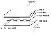
図1は、本発明の第1の実施形態の光学素子の構成を模式的に示す斜視図である。図1に示すように、光学素子1では、基板11、金属層12、高誘電率層13、蛍光体層14の順で積層されている。
FIG. 1 is a perspective view schematically showing a configuration of an optical element according to a first embodiment of the present invention. As shown in FIG. 1, in the optical element 1, a substrate 11, a metal layer 12, a high dielectric constant layer 13, and a phosphor layer 14 are laminated in this order.
なお、実際の光学素子では、各層の厚さが非常に薄く、また各層の厚さの違いが大きいので、各層を正確なスケールや比率で図示するのは困難である。このため、図面では各層が実際の比率通りに描かれておらず、模式的に示されている。また、図1に示すように、基板11と平行な面をXY平面とし、XY平面と直交する方向をZ方向とする。
In an actual optical element, the thickness of each layer is very thin and the difference in thickness between the layers is large, so that it is difficult to illustrate each layer with an accurate scale and ratio. For this reason, in the drawings, the layers are not schematically drawn but are shown schematically. As shown in FIG. 1, a plane parallel to the substrate 11 is defined as an XY plane, and a direction orthogonal to the XY plane is defined as a Z direction.
基板11の材料としては、例えば、ガラスなどが挙げられる。
Examples of the material of the substrate 11 include glass.
金属層12は、表面プラズモンを励起するプラズモン励起層である。金属層12の材料としては、例えば、金、銀、銅、白金、パラジウム、ロジウム、オスミウム、ルテニウム、イリジウム、鉄、錫、亜鉛、コバルト、ニッケル、クロム、チタン、タンタル、タングステン、インジウム、アルミニウム、又はこれらの合金などで形成される。また、金属層12の厚さは、200nm以下に形成されるのが好ましく、10nm~100nm程度に形成されるのが特に好ましい。
The metal layer 12 is a plasmon excitation layer that excites surface plasmons. Examples of the material of the metal layer 12 include gold, silver, copper, platinum, palladium, rhodium, osmium, ruthenium, iridium, iron, tin, zinc, cobalt, nickel, chromium, titanium, tantalum, tungsten, indium, aluminum, Alternatively, they are made of these alloys. Further, the thickness of the metal layer 12 is preferably formed to 200 nm or less, and particularly preferably about 10 nm to 100 nm.
高誘電率層13は、誘電率が2.25より高い誘電体で形成される誘電体層である。なお、高誘電率層13は、誘電率が高いほど望ましい。
The high dielectric constant layer 13 is a dielectric layer formed of a dielectric having a dielectric constant higher than 2.25. The higher dielectric constant layer 13 is more desirable as the dielectric constant is higher.
また、高誘電率層13では、蛍光体層14と接する面に、回折格子(グレーティング)として機能するグレーティング構造21を有する。グレーティング構造21としては、凹凸構造、フォトニック結晶およびレンズアレイなどが挙げられる。なお、凹凸構造には、凸部が円錐形状であるモスアイ構造なども含まれる。本実施形態では、グレーティング構造21を凹凸構造とする。また、凹凸構造の凹凸は、三角格子状に配置されていることが望ましいが、1次元格子状に配置されていてもよい。
Further, the high dielectric constant layer 13 has a grating structure 21 that functions as a diffraction grating (grating) on the surface in contact with the phosphor layer 14. Examples of the grating structure 21 include an uneven structure, a photonic crystal, and a lens array. Note that the concavo-convex structure includes a moth-eye structure in which the convex portion has a conical shape. In the present embodiment, the grating structure 21 is an uneven structure. Further, the unevenness of the uneven structure is desirably arranged in a triangular lattice shape, but may be disposed in a one-dimensional lattice shape.
蛍光体層14は、入射された入射光を吸光して励起子(キャリア)を生成し、その励起子によって蛍光を発生させるキャリア生成層である。蛍光体層14の材料としては、量子ドット蛍光体などのナノ無機蛍光体が望ましいが、Eu、BaMgAlxOy:Eu、BaMgAlxOy:Mnなどの無機蛍光体や有機蛍光体でもよい。
The phosphor layer 14 is a carrier generation layer that absorbs incident incident light to generate excitons (carriers) and generates fluorescence by the excitons. The material of the phosphor layer 14 is preferably a nano inorganic phosphor such as a quantum dot phosphor, but may be an inorganic phosphor such as Eu, BaMgAlxOy: Eu, BaMgAlxOy: Mn, or an organic phosphor.
以上のように構成された光学素子1において、光が蛍光体層14に入射すると、その入射した入射光は、蛍光体層14内に励起子を励起する。励起子の一部は緩和することによって蛍光に変換されて光学素子1から出射される。また、残りの励起子の一部は、金属層12と高誘電率層13との界面に表面プラズモンを励起する。励起された表面プラズモンは、グレーティング構造21によって回折されて光学素子1から出射される。
In the optical element 1 configured as described above, when light enters the phosphor layer 14, the incident light excites excitons in the phosphor layer 14. A part of the excitons is converted into fluorescence by being relaxed and emitted from the optical element 1. Some of the remaining excitons excite surface plasmons at the interface between the metal layer 12 and the high dielectric constant layer 13. The excited surface plasmon is diffracted by the grating structure 21 and emitted from the optical element 1.
上記の表面プラズモンが励起されるためには、表面プラズモンの波数のXおよびY成分の波数ksppと、回折格子の周期kgとが一致する必要がある。つまり、mを正の整数とすると、kspp=m・Kgが満たされる必要がある。
In order for the above surface plasmon to be excited, the wave number kspp of the X and Y components of the surface plasmon wave number and the period gg of the diffraction grating must match. That is, if m is a positive integer, kspp = m · Kg needs to be satisfied.
波数ksppは、光学素子1の入出射部分の誘電率分布に応じて決定される。入出射部分は、金属層12よりも高誘電率層13側にある媒質(図1では、高誘電率層13および蛍光体層14)である。
The wave number kspp is determined according to the dielectric constant distribution of the incident / exit portion of the optical element 1. The incident / exit portion is a medium (in FIG. 1, the high dielectric constant layer 13 and the phosphor layer 14) located on the high dielectric constant layer 13 side of the metal layer 12.
金属層12の誘電率の実部をεmetal、真空中での光の波数をk0とすると、表面プラズモンの波数のX成分およびY成分の波数ksppと、表面プラズモンの波数のZ成分kspp、Zとは、
If the real part of the dielectric constant of the metal layer 12 is ε metal, and the wave number of light in vacuum is k 0, the wave number kspp of the X and Y components of the surface plasmon wave number, and the Z component kspp, Z of the wave number of the surface plasmon Is


式(3)における積分範囲Dは、金属層12の高誘電率層13側の3次元範囲である。より具体的には、積分範囲DのXY平面の範囲は、金属層12内の範囲であり、積分範囲のZ方向の範囲は、金属層12および高誘電率層13の界面から高誘電率層13側の無限遠までの範囲である。なお、金属層12および高誘電率層13の界面をZ=0とし、この界面から高誘電率層13側へ遠ざかる方向を+Z方向としている。
The integration range D in Equation (3) is a three-dimensional range on the high dielectric constant layer 13 side of the metal layer 12. More specifically, the range of the XY plane of the integration range D is a range in the metal layer 12, and the range of the integration range in the Z direction is from the interface between the metal layer 12 and the high dielectric constant layer 13 to the high dielectric constant layer. It is the range up to infinity on the 13th side. Note that the interface between the metal layer 12 and the high dielectric constant layer 13 is Z = 0, and the direction away from the interface toward the high dielectric constant layer 13 is the + Z direction.
実効誘電率εeffは、以下の式を用いて計算してもよい。ただし、式(3)を用いる方が特に望ましい。
Effective dielectric constant εeff may be calculated using the following equation. However, it is particularly desirable to use equation (3).

式(1)、式(2)、式(3)を用いることで、入出射部分の誘電率分布ε(ω、x、y、z)から波数ksppを求めることができる。より具体的には、入出射部分の誘電率分布ε(ω、x、y、z)を式(3)に代入し、実効誘電率εeffに適当な初期値を与え、式(1)、式(2)、式(3)を用いて、表面プラズモンの波数ksppおよびkspp、Zと実効誘電率εeffとを繰り返し算出していくことで、実際の実効誘電率εeffを算出し、その実際の実効誘電率εeffから波数ksppを求めることができる。
By using the equations (1), (2), and (3), the wave number kspp can be obtained from the permittivity distribution ε (ω, x, y, z) of the incident / exit portion. More specifically, the dielectric constant distribution ε (ω, x, y, z) of the incident / exit portion is substituted into the equation (3), and an appropriate initial value is given to the effective dielectric constant εeff. (2) Using the equation (3), the actual effective dielectric constant εeff is calculated by repeatedly calculating the wave numbers kspp, kspp, and Z of the surface plasmon and the effective dielectric constant εeff. The wave number kspp can be obtained from the dielectric constant εeff.
したがって、式(1)、式(2)、式(3)を用いて、kspp=m・Kgが満たされるように、回折格子の周期と入出射部分の誘電率分布とを調整すれば、励起された表面プラズモンが効率的に取り出され、蛍光の増強効果を高くすることができる。
Therefore, excitation can be achieved by adjusting the period of the diffraction grating and the permittivity distribution of the incident / exit portions so that kspp = m · Kg is satisfied using Equation (1), Equation (2), and Equation (3). The surface plasmons thus obtained are efficiently extracted, and the fluorescence enhancement effect can be enhanced.
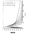
図2は、励起子と表面プラズモンの結合効率と、励起子から金属層12までの相互作用距離と、高誘電率層13の誘電率との関係を示す図である。なお、励起子および表面プラズモンの結合効率は、励起された励起子のうち表面プラズモンを励起する励起子の割合を示す。
FIG. 2 is a graph showing the relationship between the coupling efficiency between excitons and surface plasmons, the interaction distance from the excitons to the metal layer 12, and the dielectric constant of the high dielectric constant layer 13. The coupling efficiency between excitons and surface plasmons indicates the ratio of excitons that excite surface plasmons among the excited excitons.
図2で示したように、励起子から金属層12までの距離である相互作用距離が長いほど、励起子および表面プラズモンの結合効率は小さくなる。このため、励起子および表面プラズモンの結合効率が高くなるように、相互作用距離を調整して、表面プラズモンの強度を高くすることが望ましい。例えば、蛍光体層14の高誘電率層13とは反対の面から金属層12までの距離を、表面プラズモンの強度が最大値のe-2倍となる相互作用距離である有効相互作用距離程度にすればよい。なお、有効相互作用距離deffは、
As shown in FIG. 2, as the interaction distance, which is the distance from the exciton to the metal layer 12, is longer, the coupling efficiency between the exciton and the surface plasmon becomes smaller. For this reason, it is desirable to increase the strength of the surface plasmon by adjusting the interaction distance so that the coupling efficiency between the exciton and the surface plasmon becomes high. For example, the distance from the surface of the phosphor layer 14 opposite to the high dielectric constant layer 13 to the metal layer 12 is an effective interaction distance that is an interaction distance at which the surface plasmon intensity is e-2 times the maximum value. You can do it. The effective interaction distance deff is

また、実際の光学素子における有効相互作用距離deffは、数百ナノメートルオーダーとなるため、蛍光および表面プラズモンの結合効率を高くするためには、蛍光体層14の材料である蛍光材料の粒子径は、ナノメートルオーダーであることが望ましい。
In addition, since the effective interaction distance deff in an actual optical element is on the order of several hundred nanometers, in order to increase the coupling efficiency of fluorescence and surface plasmon, the particle diameter of the fluorescent material that is the material of the phosphor layer 14 Is preferably in the nanometer order.
また、図2で示したように、高誘電率層13の誘電率は高いほど、励起子および表面プラズモンの結合効率の最大値は大きくなる。このため、高誘電率層13の誘電率は高いほど望ましい。ただし、入出射部分の実効誘電率の実部が、金属層12の誘電率の実部の絶対値を大きく超えないように設定する必要がある。入出射部分の実効誘電率の実部が金属層12の誘電率の実部の絶対値を超えると、式(2)が示すとおり表面プラズモンが励起されない条件となる。実際は、金属層12の誘電率は虚数部を持つため、入出射部分の実効誘電率の実部が金属層12の誘電率の実部の絶対値を超えたとしても、表面プラズモンは励起されるが、入出射部分の実効誘電率の実部と金属層12の誘電率の実部の絶対値の乖離が大きいと、表面プラズモンが励起されなくなる。
As shown in FIG. 2, the maximum value of the coupling efficiency between excitons and surface plasmons increases as the dielectric constant of the high dielectric constant layer 13 increases. For this reason, the higher dielectric constant of the high dielectric constant layer 13 is desirable. However, it is necessary to set the real part of the effective dielectric constant of the incident / exit part not to greatly exceed the absolute value of the real part of the dielectric constant of the metal layer 12. When the real part of the effective dielectric constant of the incident / exit part exceeds the absolute value of the real part of the dielectric constant of the metal layer 12, the condition that the surface plasmon is not excited as shown in the equation (2). Actually, since the dielectric constant of the metal layer 12 has an imaginary part, the surface plasmon is excited even if the real part of the effective dielectric constant of the input / output part exceeds the absolute value of the real part of the dielectric constant of the metal layer 12. However, if the difference between the absolute values of the real part of the effective dielectric constant of the incident / exit part and the real part of the dielectric constant of the metal layer 12 is large, the surface plasmon is not excited.
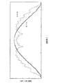
図3は、光学素子からの出射光の光強度および放射角の関係を示す図である。具体的には、高誘電率層13の誘電率が従来の値である2.25の場合と、高誘電率層13の誘電率が従来の値より大きい6.25の場合における、光学素子1からの出射光の光強度および放射角の関係を示す図である。ここで、縦軸の光強度は極角ごとの光の状態密度について規格化した値である。
FIG. 3 is a diagram showing the relationship between the light intensity of the light emitted from the optical element and the radiation angle. Specifically, the optical element 1 in the case where the dielectric constant of the high dielectric constant layer 13 is 2.25 which is a conventional value and in the case where the dielectric constant of the high dielectric constant layer 13 is 6.25 which is larger than the conventional value. It is a figure which shows the relationship between the light intensity and the radiation angle of the emitted light from. Here, the light intensity on the vertical axis is a value normalized with respect to the state density of light for each polar angle.
図3に示すように、高誘電率層13の誘電率が6.25の場合、高誘電率層13の誘電率が2.25の場合と比べて、放射角が-45°~45°に含まれる出射光の光強度は、1.1倍になり、放射角が-60°~60°に含まれる出射光の光強度は、1.2倍になる。
As shown in FIG. 3, when the dielectric constant of the high dielectric constant layer 13 is 6.25, the radiation angle is −45 ° to 45 ° compared to the case where the dielectric constant of the high dielectric constant layer 13 is 2.25. The light intensity of the included outgoing light is 1.1 times, and the light intensity of the outgoing light included in the radiation angle of −60 ° to 60 ° is 1.2 times.
以上説明したように本実施形態によれば、金属層12、誘電率が2.25より高い高誘電率層13、入射光によって蛍光が発生する蛍光体層14の順で積層されて、高誘電率層13および蛍光体層14の界面には、回折格子が形成される。このため、蛍光体層14で発生する蛍光と金属層12で発生する表面プラズモンとの結合効率を高くすることが可能になり、表面プラズモンから変換される蛍光の光強度が高くなる。そして、蛍光がグレーティング構造21によって出射角度が変換されるので、指向性も高くすることが可能になる。
As described above, according to the present embodiment, the metal layer 12, the high dielectric constant layer 13 having a dielectric constant higher than 2.25, and the phosphor layer 14 that generates fluorescence by incident light are laminated in this order to obtain a high dielectric constant. A diffraction grating is formed at the interface between the index layer 13 and the phosphor layer 14. For this reason, it becomes possible to increase the coupling efficiency between the fluorescence generated in the phosphor layer 14 and the surface plasmon generated in the metal layer 12, and the light intensity of the fluorescence converted from the surface plasmon is increased. Since the emission angle of the fluorescence is converted by the grating structure 21, the directivity can be increased.
次に本発明の他の実施形態について説明する。
Next, another embodiment of the present invention will be described.
図4~図9は、蛍光体層14の一例を示す図であり、光学素子1をYZ平面で切断した断面と、光学素子1を+Z方向から見た上面とが示されている。
4 to 9 are diagrams showing an example of the phosphor layer 14, and shows a cross section of the optical element 1 cut along the YZ plane and an upper surface of the optical element 1 viewed from the + Z direction.
図4の例では、蛍光体層14が高誘電率層13を覆っている。また、蛍光体層14の高誘電率層13と接する面の逆の面が平坦となっている。
In the example of FIG. 4, the phosphor layer 14 covers the high dielectric constant layer 13. Further, the surface opposite to the surface in contact with the high dielectric constant layer 13 of the phosphor layer 14 is flat.
図5の例では、蛍光体層14は、高誘電率層13の凹部に埋め込まれており、蛍光体層14の高さと高誘電率層13の凸部の高さが同じになっている。
In the example of FIG. 5, the phosphor layer 14 is embedded in the concave portion of the high dielectric constant layer 13, and the height of the phosphor layer 14 and the height of the convex portion of the high dielectric constant layer 13 are the same.
図6の例では、蛍光体層14は、高誘電率層13の凹部に埋め込まれており、蛍光体層14の高さは高誘電率層13の凸部の高さより小さくなっている。
In the example of FIG. 6, the phosphor layer 14 is embedded in the concave portion of the high dielectric constant layer 13, and the height of the phosphor layer 14 is smaller than the height of the convex portion of the high dielectric constant layer 13.
図7の例では、高誘電率層13の凹部に埋め込まれており、蛍光体層14の高さと高誘電率層13の凸部の高さが同じになっている。また、蛍光体層14は、高誘電率層13の凸部にも積層されている。
In the example of FIG. 7, it is embedded in the concave portion of the high dielectric constant layer 13, and the height of the phosphor layer 14 and the height of the convex portion of the high dielectric constant layer 13 are the same. The phosphor layer 14 is also laminated on the convex portion of the high dielectric constant layer 13.
図8の例では、蛍光体層14が高誘電率層13を覆っている。また、蛍光体層14の高誘電率層13と接する面の逆の面は、高誘電率層13のグレーティング構造21と同じ構造が形成されている。
In the example of FIG. 8, the phosphor layer 14 covers the high dielectric constant layer 13. Further, the same structure as the grating structure 21 of the high dielectric constant layer 13 is formed on the surface opposite to the surface in contact with the high dielectric constant layer 13 of the phosphor layer 14.
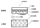
図9の例では、蛍光体層14に、入射光の見かけの吸光度を増大させるための金属微粒子31が含まれている。見かけの吸光度とは、蛍光体層14を、均質な層とみなし、蛍光体層14全面に光を入射させたときの吸光度である。金属微粒子31は、入射光と相互作用することにより、金属微粒子31の表面に表面プラズモンを励起し、その表面近傍に入射光の電場強度に対して100倍近くの大きさの増強電場を誘起する。この増強電場によっても蛍光体層14内に励起子が生成されるので、蛍光体層14内の励起子の数が増加する。このため、金属微粒子31は、自身の表面に励起された表面プラズモンによって、入射光の見かけの吸光度を増大させて、蛍光の光強度を増大させることができる。
In the example of FIG. 9, the phosphor layer 14 contains metal fine particles 31 for increasing the apparent absorbance of incident light. The apparent absorbance is the absorbance when the phosphor layer 14 is regarded as a homogeneous layer and light is incident on the entire surface of the phosphor layer 14. The metal fine particles 31 interact with the incident light to excite surface plasmons on the surface of the metal fine particles 31, and induce an enhanced electric field in the vicinity of the surface with a magnitude nearly 100 times the electric field intensity of the incident light. . Since the excitons are also generated in the phosphor layer 14 by this enhanced electric field, the number of excitons in the phosphor layer 14 increases. For this reason, the metal fine particles 31 can increase the apparent absorbance of the incident light and increase the light intensity of the fluorescence by the surface plasmon excited on its surface.
金属微粒子31の材料としては、例えば、金、銀、銅、白金、パラジウム、ロジウム、オスミウム、ルテニウム、イリジウム、鉄、錫、亜鉛、コバルト、ニッケル、クロム、チタン、タンタル、タングステン、インジウム、アルミニウム、又はこれらの合金などが挙げられる。これらの中でも、金、銀、銅、白金、アルミニウムまたはこれらを主成分とする合金が好ましく、金、銀、アルミニウムまたはこれらを主成分とする合金が特に好ましい。金属微粒子31はその周辺と中心で金属種の異なるコアシェル構造、2種の半球の合体した半球合体構造、異なるクラスターが集合して微粒子を作るクラスター・イン・クラスター構造でもよい。金属微粒子31を合金または、これら特殊構造とすることで、微粒子の寸法や、形状を変化させなくとも、共鳴波長を制御できる。
Examples of the material of the metal fine particles 31 include gold, silver, copper, platinum, palladium, rhodium, osmium, ruthenium, iridium, iron, tin, zinc, cobalt, nickel, chromium, titanium, tantalum, tungsten, indium, aluminum, Or these alloys etc. are mentioned. Among these, gold, silver, copper, platinum, aluminum, or an alloy containing these as a main component is preferable, and gold, silver, aluminum, or an alloy containing these as a main component is particularly preferable. The metal fine particles 31 may have a core-shell structure in which the metal species are different in the periphery and the center, a hemispherical union structure in which two hemispheres are merged, or a cluster-in-cluster structure in which different clusters gather to form fine particles. By making the metal fine particles 31 into an alloy or a special structure thereof, the resonance wavelength can be controlled without changing the size or shape of the fine particles.
金属微粒子31の形状としては、直方体、立方体、楕円体、球体、三角錐および三角柱など、閉じた表面を有する形状であればどのような形状でも良い。また、金属微粒子31には、半導体リソグラフィ技術に代表される微細加工によって、金属薄膜を一辺が10μm未満の閉じた面で構成される構造体に加工したものも含まれる。
The shape of the metal fine particles 31 may be any shape as long as it has a closed surface, such as a rectangular parallelepiped, a cube, an ellipsoid, a sphere, a triangular pyramid, and a triangular prism. Further, the metal fine particles 31 include those obtained by processing a metal thin film into a structure composed of a closed surface with a side of less than 10 μm by fine processing typified by semiconductor lithography technology.
図10は、光学素子の別の形態を示す図である。図10において、光学素子1’は、図1で示した光学素子1に加えて、蛍光体層14の上に設けられた冷却層15と、光学素子1および冷却層15を覆うカバー17とをさらに有する。
FIG. 10 is a diagram showing another form of the optical element. 10, in addition to the optical element 1 shown in FIG. 1, the optical element 1 ′ includes a cooling layer 15 provided on the phosphor layer 14, and a cover 17 that covers the optical element 1 and the cooling layer 15. Also have.
冷却層15は、例えば、オイルなどの透明な液体などで形成され、蛍光体層14を冷却する。また、カバー17には、冷却層15の上の箇所に光透過部16が備わっている。光透過部16は、例えば、ガラスなどの透明誘電体のような光を透過する物質で形成され、蛍光体層14に入射する入射光と、蛍光体層14で発生する蛍光とを透過する。なお、光透過部16には、入射光および蛍光の反射を抑制して、入射光および蛍光の透過率を向上させる構造体が形成されてもよい。この構造体としては、フォトニック結晶、モスアイ構造、レンズアレイなどが挙げられる。
The cooling layer 15 is formed of, for example, a transparent liquid such as oil, and cools the phosphor layer 14. Further, the cover 17 is provided with a light transmission part 16 at a location above the cooling layer 15. The light transmission part 16 is formed of a material that transmits light such as a transparent dielectric such as glass, and transmits incident light incident on the phosphor layer 14 and fluorescence generated in the phosphor layer 14. The light transmitting portion 16 may be formed with a structure that suppresses the reflection of incident light and fluorescence and improves the transmittance of incident light and fluorescence. Examples of this structure include a photonic crystal, a moth-eye structure, and a lens array.
次に光学素子1を用いた照明装置について説明する。
Next, an illumination device using the optical element 1 will be described.
図11は、照明装置40を示す図である。図11において、照明装置40は、光学素子1と、光源41と、光源からの光が入射する導光体42と、ダイクロイックミラー43とを有する。
FIG. 11 is a diagram showing the lighting device 40. In FIG. 11, the illumination device 40 includes the optical element 1, a light source 41, a light guide 42 on which light from the light source is incident, and a dichroic mirror 43.
光源41は、例えば、LED(Light Emitting Diode)などで構成され、導光体42の外周部に配置される。光源41は、導光体42を介して光学素子1の蛍光体層14に光を入射する。
The light source 41 is composed of, for example, an LED (Light Emitting Diode) or the like, and is disposed on the outer periphery of the light guide 42. The light source 41 makes light incident on the phosphor layer 14 of the optical element 1 through the light guide 42.
なお、図11では、光源41は、導光体42と接触するように配置されているが、導光体42から離れた位置に配置されてもよく、例えばライトパイプのような導光部材によって導光体42と光学的に接続されてもよい。
In FIG. 11, the light source 41 is disposed so as to contact the light guide 42, but may be disposed at a position away from the light guide 42, for example, by a light guide member such as a light pipe. The light guide 42 may be optically connected.
導光体42は、例えばガラスで形成された平板状の部材であり、光源41から入射した光を内部で伝播させる。
The light guide 42 is a flat plate member made of glass, for example, and propagates light incident from the light source 41 inside.
導光体42の第1の面には、光学素子1が設けられている。なお、導光体42の第1の面と光学素子1の蛍光体層14が対向している。
The optical element 1 is provided on the first surface of the light guide 42. In addition, the 1st surface of the light guide 42 and the fluorescent substance layer 14 of the optical element 1 are facing.
導光体42の第1の面とは反対の面である第2の面には、ダイクロイックミラー43が設けられている。
A dichroic mirror 43 is provided on the second surface opposite to the first surface of the light guide 42.
ダイクロイックミラー43は、光源41から入射した光を反射し、光学素子1で発生した蛍光を透過する波長選択性部材である。
The dichroic mirror 43 is a wavelength selective member that reflects the light incident from the light source 41 and transmits the fluorescence generated by the optical element 1.
以上のように構成された照明装置において、光源41から光が出射されると、その光は導光体42に入射され、導光体42内部を伝播する。導光体42内部では、光は、直接、または、ダイクロイックミラー43で反射され、光学素子1の蛍光体層14に入射する。その蛍光体層14に入射した光の一部は、蛍光体層14で反射され再び導光体42に戻される。この戻された光は、ダイクロイックミラー43で反射され蛍光体層14に再入射する。
In the illuminating device configured as described above, when light is emitted from the light source 41, the light is incident on the light guide 42 and propagates inside the light guide 42. In the light guide 42, the light is reflected directly or by the dichroic mirror 43 and enters the phosphor layer 14 of the optical element 1. Part of the light incident on the phosphor layer 14 is reflected by the phosphor layer 14 and returned to the light guide 42 again. The returned light is reflected by the dichroic mirror 43 and reenters the phosphor layer 14.
また、蛍光体層14に入射した光の一部は、第1の実施形態で説明したように蛍光に変換されて、蛍光体層14から導光体42に出射される。そして、導光体42に出射された光はダイクロイックミラー43を透過して出射される。
Further, part of the light incident on the phosphor layer 14 is converted into fluorescence as described in the first embodiment, and is emitted from the phosphor layer 14 to the light guide 42. The light emitted to the light guide 42 is transmitted through the dichroic mirror 43 and emitted.
また、照明装置40では、図12に示すように、ダイクロイックミラー43の導光体42の反対の面には、蛍光体層14からの蛍光の反射を抑制して、蛍光の透過率を向上させる構造体44が設けられてもよい。構造体44としては、フォトニック結晶、モスアイ構造およびレンズアレイなどが挙げられる。
Further, in the illumination device 40, as shown in FIG. 12, the reflection of the fluorescence from the phosphor layer 14 is suppressed on the surface opposite to the light guide 42 of the dichroic mirror 43 to improve the fluorescence transmittance. A structure 44 may be provided. Examples of the structure 44 include a photonic crystal, a moth-eye structure, and a lens array.
次に光学素子1を用いたカラーホイールについて説明する。
Next, a color wheel using the optical element 1 will be described.
カラーホイールは、例えば、プロジェクタなどにおいて、カラー画像を表示するために使用されるものであり、入射された光を複数の色の光に変換し時分割して出射するためのものである。
The color wheel is used, for example, in a projector or the like to display a color image, and converts incident light into light of a plurality of colors and emits it in a time-division manner.
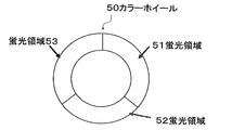
図13は、光学素子を用いたカラーホイールを示す正面図である。図13において、カラーホイール50は、蛍光領域51~53を有する。蛍光領域51~53は、光学素子1または1’で構成される。また、各蛍光領域51~53における光学素子1の蛍光体層14は、それぞれ異なる色の蛍光を発生させる。
FIG. 13 is a front view showing a color wheel using an optical element. In FIG. 13, the color wheel 50 has fluorescent regions 51-53. The fluorescent regions 51 to 53 are constituted by the optical element 1 or 1 '. Further, the phosphor layer 14 of the optical element 1 in each of the fluorescent regions 51 to 53 generates fluorescence of different colors.
図13の例では、カラーホイール50は、円形であり、外周部が3等分され、その3等分された各部分が蛍光領域51~53になっている。
In the example of FIG. 13, the color wheel 50 is circular, the outer periphery is divided into three equal parts, and each of the three parts divided into fluorescent regions 51 to 53.
通常、カラーホイール50は、そのカラーホイール50の中心に直交する軸を回転軸として回転され、光源からの光がカラーホイール50の外周部に照射されるように使用される。これにより、光が入射される領域が蛍光領域51~53に時分割されるので、入射された光を複数の色の光に変換し時分割して出射することができる。
Usually, the color wheel 50 is rotated so that the axis orthogonal to the center of the color wheel 50 is a rotation axis, and the light from the light source is used to irradiate the outer peripheral portion of the color wheel 50. As a result, the region where the light is incident is time-divided into the fluorescent regions 51 to 53, so that the incident light can be converted into a plurality of colors and emitted in a time-division manner.
なお、カラーホイールは、光学素子1または1’で構成される蛍光領域が少なくとも一つあればよく、図14に示すカラーホイール50’のように、外周部は、蛍光領域51と、光を透過する透過領域54とに2等分されてもよい。なお、透過領域54は、すりガラスのような光を拡散して透過する光拡散板で形成されてもよい。
The color wheel only needs to have at least one fluorescent region composed of the optical element 1 or 1 ′, and the outer peripheral portion transmits light with the fluorescent region 51 as in the color wheel 50 ′ shown in FIG. The transmission region 54 may be divided into two equal parts. The transmission region 54 may be formed of a light diffusion plate that diffuses and transmits light such as ground glass.
次に光学素子を用いたプロジェクタ(投射型表示装置)について説明する。
Next, a projector (projection display device) using an optical element will be described.
図15は、光学素子を用いたプロジェクタの一例を示す図である。図15において、プロジェクタは、光学素子1A~1Cと、光源101A~101Cと、ダイクロイックミラー102A~102Cと、表示素子103A~103Cと、色合成プリズム104と、投射レンズ105とを有する。なお、光学素子1A~1Cおよび光源101A~101Cは、照明装置を構成する。
FIG. 15 is a diagram showing an example of a projector using an optical element. In FIG. 15, the projector includes optical elements 1A to 1C, light sources 101A to 101C, dichroic mirrors 102A to 102C, display elements 103A to 103C, a color synthesis prism 104, and a projection lens 105. The optical elements 1A to 1C and the light sources 101A to 101C constitute an illumination device.
光学素子1A~1Cは、光学素子1または1’で構成される。なお、各光学素子1A~1Cにおける蛍光体層14は、それぞれ異なる色の蛍光を発生させる。例えば、各光学素子1A~1Cにおける蛍光体層14は、赤色、緑色および青色のそれぞれの蛍光を発生させる。
The optical elements 1A to 1C are constituted by the optical element 1 or 1 '. Note that the phosphor layer 14 in each of the optical elements 1A to 1C generates fluorescence of different colors. For example, the phosphor layer 14 in each of the optical elements 1A to 1C generates red, green, and blue fluorescence.
光源101A~101Cは、光学素子1A~1Cのそれぞれで蛍光を発生させることが可能な波長の光を出射する。本実施形態では、ダイクロイックミラー102A~102Cのそれぞれは、光源101A~101Cのそれぞれの光を透過して光学素子1A~1Cのそれぞれに入射する。また、ダイクロイックミラー102A~102Cのそれぞれは、光学素子1A~1Cのそれぞれの蛍光体層14から出射された蛍光を反射して表示素子103A~103Cのそれぞれに入射する。
The light sources 101A to 101C emit light having a wavelength capable of generating fluorescence in each of the optical elements 1A to 1C. In the present embodiment, each of the dichroic mirrors 102A to 102C transmits the light of each of the light sources 101A to 101C and enters each of the optical elements 1A to 1C. Further, each of the dichroic mirrors 102A to 102C reflects the fluorescence emitted from the respective phosphor layers 14 of the optical elements 1A to 1C, and enters each of the display elements 103A to 103C.
表示素子103A~103Cのそれぞれは、ダイクロイックミラー102A~102Cのそれぞれからの蛍光を入力映像信号に応じて変調して色合成プリズム104に出射する。
Each of the display elements 103A to 103C modulates the fluorescence from each of the dichroic mirrors 102A to 102C in accordance with the input video signal and emits it to the color synthesis prism 104.
色合成プリズム104は、表示素子103A~103Cのそれぞれからの蛍光を合成して投射レンズ105を介して出射する。
The color synthesizing prism 104 synthesizes fluorescence from each of the display elements 103A to 103C and emits it through the projection lens 105.
なお、色合成プリズム104および投射レンズ105は投射光学系に含まれる。
Note that the color synthesis prism 104 and the projection lens 105 are included in the projection optical system.
図16は、光学素子を用いたプロジェクタの他の例を示す図である。図16で示すプロジェクタは、図15で示した構成に加えて、集光レンズ106A~106Cをさらに有する。
FIG. 16 is a diagram showing another example of a projector using an optical element. The projector shown in FIG. 16 further includes condenser lenses 106A to 106C in addition to the configuration shown in FIG.
集光レンズ106A~106Cのそれぞれは、光学素子1A~1Cのそれぞれとダイクロイックミラー102A~102Cのそれぞれの間に設けられる。集光レンズ106A~106Cは、ダイクロイックミラー102A~102Cのそれぞれを透過した光と、光学素子1A~1Cのそれぞれから出射された蛍光とを集光する。
The condenser lenses 106A to 106C are provided between the optical elements 1A to 1C and the dichroic mirrors 102A to 102C, respectively. The condensing lenses 106A to 106C condense the light transmitted through the dichroic mirrors 102A to 102C and the fluorescence emitted from the optical elements 1A to 1C, respectively.
図17は、光学素子を用いたプロジェクタの他の例を示す図である。
FIG. 17 is a diagram showing another example of a projector using an optical element.
図17で示すプロジェクタは、照明装置201A~201Cと、表示素子202A~202Cと、色合成プリズム203と、投射レンズ204とを有する。
The projector shown in FIG. 17 includes lighting devices 201A to 201C, display elements 202A to 202C, a color synthesis prism 203, and a projection lens 204.
照明装置201A~201Cは、図11または図12で示した照明装置40で構成される。なお、各照明装置201A~201Cにおける蛍光体層14は、それぞれ異なる色の蛍光を発生させる。例えば、各照明装置201A~201Cにおける蛍光体層14は、赤色、緑色および青色のそれぞれの蛍光を発生させる。
The lighting devices 201A to 201C are configured by the lighting device 40 shown in FIG. 11 or FIG. Note that the phosphor layer 14 in each of the lighting devices 201A to 201C generates fluorescence of different colors. For example, the phosphor layer 14 in each of the lighting devices 201A to 201C generates red, green, and blue fluorescence.
表示素子202A~202Cのそれぞれは、照明装置201A~201Cのそれぞれからの蛍光を入力映像信号に応じて変調して色合成プリズム203に出射する。
Each of the display elements 202A to 202C modulates the fluorescence from each of the illumination devices 201A to 201C in accordance with the input video signal and emits the modulated light to the color synthesis prism 203.
色合成プリズム203は、表示素子202A~202Cのそれぞれからの蛍光を合成して投射レンズ204を介して出射する。
The color synthesis prism 203 synthesizes the fluorescence from each of the display elements 202A to 202C and emits it through the projection lens 204.
図18は、光学素子を用いたプロジェクタの他の例を示す図である。図18において、プロジェクタは、光源301Aおよび301Bと、カラーホイール302と、反射ミラー303と、集光レンズ304および306と、ダイクロイックミラー305と、表示素子307と、投射レンズ308とを有する。なお、光源301A、301Bおよびカラーホイール302は照明装置を構成する。
FIG. 18 is a diagram showing another example of a projector using an optical element. 18, the projector includes light sources 301A and 301B, a color wheel 302, a reflection mirror 303, condenser lenses 304 and 306, a dichroic mirror 305, a display element 307, and a projection lens 308. Note that the light sources 301A and 301B and the color wheel 302 constitute an illumination device.
光源301Aおよび301Bは、互いに異なる色の光を出射する。本実施形態では、光源301Aは青色光を出射し、光源301Bは赤色光を出射するものとする。
The light sources 301A and 301B emit light of different colors. In the present embodiment, the light source 301A emits blue light, and the light source 301B emits red light.
カラーホイール302は、図14に示したカラーホイール50’と同じ構成を有する。カラーホイール302の蛍光体層14は、青色光が入射されると、蛍光として緑色光を出射するものとする。この場合、カラーホイール302の透過領域54が青色光を透過するので、青色光と緑色光を時分割して出射することになる。なお、カラーホイール302は、透過された青色光が反射ミラー303に入射され、蛍光として出射された緑色光が集光レンズ304を介してダイクロイックミラー305に入射されるように配置される。
The color wheel 302 has the same configuration as the color wheel 50 'shown in FIG. The phosphor layer 14 of the color wheel 302 emits green light as fluorescence when blue light is incident thereon. In this case, since the transmission region 54 of the color wheel 302 transmits blue light, the blue light and the green light are emitted in a time-sharing manner. The color wheel 302 is arranged such that the transmitted blue light is incident on the reflection mirror 303 and the green light emitted as fluorescence is incident on the dichroic mirror 305 via the condenser lens 304.
反射ミラー303は、入射した青色光を反射して集光レンズ306を介して表示素子307に入射する。
The reflection mirror 303 reflects the incident blue light and enters the display element 307 via the condenser lens 306.
ダイクロイックミラー305は、青色光および赤色光を透過し、緑色光を反射する。より具体的には、ダイクロイックミラー305は、光源301Aからの青色光を透過して集光レンズ304を介してカラーホイール302に入射する。また、ダイクロイックミラー305は、光源301Bからの赤色光を透過して集光レンズ306を介して表示素子307に入射する。そして、ダイクロイックミラー305は、カラーホイール302からの緑色光を反射して集光レンズ306を介して表示素子307に入射する。
The dichroic mirror 305 transmits blue light and red light and reflects green light. More specifically, the dichroic mirror 305 transmits the blue light from the light source 301 </ b> A and enters the color wheel 302 via the condenser lens 304. Further, the dichroic mirror 305 transmits red light from the light source 301 </ b> B and enters the display element 307 through the condenser lens 306. The dichroic mirror 305 reflects the green light from the color wheel 302 and enters the display element 307 via the condenser lens 306.
表示素子307は、例えば、デジタルミラーデバイス(Digital Micromirror Device)であり、入射された赤色光、緑色光および青色光を入力映像信号に応じて変調して投射レンズ308を介して投射する。
The display element 307 is a digital mirror device (Digital Micromirror Device), for example, and modulates incident red light, green light, and blue light according to the input video signal, and projects the modulated light through the projection lens 308.
以上説明した各実施形態において、図示した構成は単なる一例であって、本発明はその構成に限定されるものではない。
In each of the embodiments described above, the illustrated configuration is merely an example, and the present invention is not limited to the configuration.
例えば、図13に示したカラーホイール50を使用したプロジェクタなども本発明には含まれる。
For example, a projector using the color wheel 50 shown in FIG. 13 is also included in the present invention.
この出願は、2011年4月7日に出願された日本出願特願2011-085364号公報、および、2012年1月6日に出願された日本出願特願2012-001320号公報を基礎とする優先権を主張し、その開示の全てをここに取り込む。
This application is based on Japanese Patent Application No. 2011-085364 filed on Apr. 7, 2011 and Japanese Patent Application No. 2012-001320 filed on Jan. 6, 2012. Claims the right and incorporates all of its disclosure here.
1、1’ 光学素子
11 基板
12 金属層
13 高誘電率層
14 蛍光体層
15 冷却層
16 カバー
21 グレーティング構造
31 微粒子
41 光源
42 導光体
43 ダイクロイックミラー
44 構造体
50、50’ カラーホイール
51~53 蛍光領域
54 透過領域 DESCRIPTION OF SYMBOLS 1, 1 'Optical element 11 Board | substrate 12 Metal layer 13 High dielectric constant layer 14 Phosphor layer 15 Cooling layer 16 Cover 21 Grating structure 31 Fine particle 41 Light source 42Light guide 43 Dichroic mirror 44 Structure 50, 50' Color wheel 51- 53 Fluorescence area 54 Transmission area
11 基板
12 金属層
13 高誘電率層
14 蛍光体層
15 冷却層
16 カバー
21 グレーティング構造
31 微粒子
41 光源
42 導光体
43 ダイクロイックミラー
44 構造体
50、50’ カラーホイール
51~53 蛍光領域
54 透過領域 DESCRIPTION OF SYMBOLS 1, 1 'Optical element 11 Board | substrate 12 Metal layer 13 High dielectric constant layer 14 Phosphor layer 15 Cooling layer 16 Cover 21 Grating structure 31 Fine particle 41 Light source 42
Claims (9)
- 金属層と、
前記金属層に積層された誘電体層と、
前記誘電体層に積層され、入射した光によって蛍光を発する蛍光体層と、を有し、
前記誘電体層および前記蛍光体層の界面には、回折格子が形成され、
前記誘電体層の誘電率は、2.25よりも高い、光学素子。 A metal layer,
A dielectric layer laminated to the metal layer;
A phosphor layer that is laminated on the dielectric layer and emits fluorescence by incident light;
At the interface between the dielectric layer and the phosphor layer, a diffraction grating is formed,
An optical element, wherein the dielectric layer has a dielectric constant higher than 2.25. - 請求項1に記載の光学素子おいて、
前記蛍光体層は、前記光によって表面プラズモンが励起される金属微粒子を有する、光学素子。 The optical element according to claim 1,
The phosphor layer is an optical element having metal fine particles whose surface plasmons are excited by the light. - 請求項1または2に記載の光学素子において、
前記蛍光体層、前記誘電体層および前記金属層を覆い、前記蛍光体層の上に前記光および前記蛍光を透過する光透過部を備えるカバーと、
前記カバーおよび前記蛍光体層の間に設けられた、前記蛍光体層を冷却する冷却層と、をさらに有する光学素子。 The optical element according to claim 1 or 2,
A cover that covers the phosphor layer, the dielectric layer, and the metal layer, and includes a light transmission portion that transmits the light and the fluorescence on the phosphor layer;
An optical element further comprising a cooling layer provided between the cover and the phosphor layer for cooling the phosphor layer. - 請求項1ないし3のいずれか1項に記載の光学素子において、
前記蛍光体層に積層され、光源からの光を伝播して前記蛍光体層に出射する導光体と、
前記導光体の前記蛍光体層が設けられた面とは逆の面に設けられ、前記光源からの光を反射し、前記蛍光を透過する波長選択性部材と、を有する光学素子。 The optical element according to any one of claims 1 to 3,
A light guide that is laminated on the phosphor layer, propagates light from a light source and emits the light to the phosphor layer;
An optical element having a wavelength selective member that is provided on a surface opposite to the surface on which the phosphor layer of the light guide is provided, reflects light from the light source, and transmits the fluorescence. - 請求項4に記載の光学素子において、
前記波長選択性部材の前記導光体が設けられた面とは逆の面に設けられ、前記蛍光の反射を抑制する構造体と、を有する光学素子。 The optical element according to claim 4,
An optical element comprising: a structure that is provided on a surface opposite to the surface on which the light guide of the wavelength selective member is provided, and that suppresses reflection of the fluorescence. - 請求項1ないし3のいずれか1項に記載の光学素子を有するカラーホイール。 A color wheel having the optical element according to any one of claims 1 to 3.
- 請求項1ないし5のいずれか1項に記載の光学素子と、
前記光学素子の蛍光体層に光を出射する光源と、を有する照明装置。 An optical element according to any one of claims 1 to 5,
And a light source that emits light to the phosphor layer of the optical element. - 請求項6に記載のカラーホイールと、
前記カラーホイールの蛍光体層に光を出射する光源と、を有する照明装置。 A color wheel according to claim 6;
And a light source that emits light to the phosphor layer of the color wheel. - 請求項7または8に記載の照明装置を有する投射型表示装置。 A projection display device having the illumination device according to claim 7 or 8.
Priority Applications (1)
| Application Number | Priority Date | Filing Date | Title |
|---|---|---|---|
| JP2013508801A JPWO2012137583A1 (en) | 2011-04-07 | 2012-03-15 | Optical element, color wheel, illumination device, and projection display device |
Applications Claiming Priority (4)
| Application Number | Priority Date | Filing Date | Title |
|---|---|---|---|
| JP2011-085364 | 2011-04-07 | ||
| JP2011085364 | 2011-04-07 | ||
| JP2012001320 | 2012-01-06 | ||
| JP2012-001320 | 2012-01-06 |
Publications (1)
| Publication Number | Publication Date |
|---|---|
| WO2012137583A1 true WO2012137583A1 (en) | 2012-10-11 |
Family
ID=46968987
Family Applications (1)
| Application Number | Title | Priority Date | Filing Date |
|---|---|---|---|
| PCT/JP2012/056729 WO2012137583A1 (en) | 2011-04-07 | 2012-03-15 | Optical element, color wheel, illumination device, and projection display device |
Country Status (2)
| Country | Link |
|---|---|
| JP (1) | JPWO2012137583A1 (en) |
| WO (1) | WO2012137583A1 (en) |
Cited By (12)
| Publication number | Priority date | Publication date | Assignee | Title |
|---|---|---|---|---|
| JP2016099520A (en) * | 2014-11-21 | 2016-05-30 | 日亜化学工業株式会社 | Wavelength conversion member and projector including the wavelength conversion member |
| JP2016170382A (en) * | 2015-03-13 | 2016-09-23 | パナソニックIpマネジメント株式会社 | Display device and light-emitting device |
| JP2016218367A (en) * | 2015-05-25 | 2016-12-22 | スタンレー電気株式会社 | Wavelength conversion member, and luminaire using the same |
| WO2016208644A1 (en) * | 2015-06-24 | 2016-12-29 | コニカミノルタ株式会社 | Optical device, light source device and projection device |
| WO2016208645A1 (en) * | 2015-06-25 | 2016-12-29 | コニカミノルタ株式会社 | Optical device, light source device and projection device |
| JP2017040905A (en) * | 2015-08-20 | 2017-02-23 | パナソニックIpマネジメント株式会社 | Light-emitting device |
| WO2017038000A1 (en) * | 2015-08-28 | 2017-03-09 | パナソニックIpマネジメント株式会社 | Lighting apparatus and lighting system |
| JP2018511080A (en) * | 2015-03-13 | 2018-04-19 | ダウ グローバル テクノロジーズ エルエルシー | Methods and devices for nanostructured materials |
| TWI634380B (en) * | 2015-12-31 | 2018-09-01 | 深圳市光峰光電技術有限公司 | Color wheel module and light source module |
| US10359155B2 (en) | 2015-08-20 | 2019-07-23 | Panasonic Intellectual Property Management Co., Ltd. | Light-emitting apparatus |
| WO2019171775A1 (en) * | 2018-03-06 | 2019-09-12 | ソニー株式会社 | Light-emitting element, light source device, and projector |
| USRE49093E1 (en) | 2015-03-13 | 2022-06-07 | Panasonic Intellectual Property Management Co., Ltd. | Light-emitting apparatus including photoluminescent layer |
Citations (6)
| Publication number | Priority date | Publication date | Assignee | Title |
|---|---|---|---|---|
| JP2007240361A (en) * | 2006-03-09 | 2007-09-20 | Sekisui Chem Co Ltd | Localized plasmon enhancing sensor |
| JP2009239217A (en) * | 2008-03-28 | 2009-10-15 | Nikon Corp | Light-emitting diode element |
| JP2011013315A (en) * | 2009-06-30 | 2011-01-20 | Casio Computer Co Ltd | Fluorescent substrate, light source device, and projector |
| WO2011040528A1 (en) * | 2009-09-30 | 2011-04-07 | 日本電気株式会社 | Optical element, light source device, and projection display device |
| WO2011108138A1 (en) * | 2010-03-04 | 2011-09-09 | 日本電気株式会社 | Optical element, light-source apparatus, and projection-type display apparatus |
| WO2012049905A1 (en) * | 2010-10-15 | 2012-04-19 | 日本電気株式会社 | Optical device, light source and projection display |
-
2012
- 2012-03-15 WO PCT/JP2012/056729 patent/WO2012137583A1/en active Application Filing
- 2012-03-15 JP JP2013508801A patent/JPWO2012137583A1/en active Pending
Patent Citations (6)
| Publication number | Priority date | Publication date | Assignee | Title |
|---|---|---|---|---|
| JP2007240361A (en) * | 2006-03-09 | 2007-09-20 | Sekisui Chem Co Ltd | Localized plasmon enhancing sensor |
| JP2009239217A (en) * | 2008-03-28 | 2009-10-15 | Nikon Corp | Light-emitting diode element |
| JP2011013315A (en) * | 2009-06-30 | 2011-01-20 | Casio Computer Co Ltd | Fluorescent substrate, light source device, and projector |
| WO2011040528A1 (en) * | 2009-09-30 | 2011-04-07 | 日本電気株式会社 | Optical element, light source device, and projection display device |
| WO2011108138A1 (en) * | 2010-03-04 | 2011-09-09 | 日本電気株式会社 | Optical element, light-source apparatus, and projection-type display apparatus |
| WO2012049905A1 (en) * | 2010-10-15 | 2012-04-19 | 日本電気株式会社 | Optical device, light source and projection display |
Cited By (17)
| Publication number | Priority date | Publication date | Assignee | Title |
|---|---|---|---|---|
| JP2016099520A (en) * | 2014-11-21 | 2016-05-30 | 日亜化学工業株式会社 | Wavelength conversion member and projector including the wavelength conversion member |
| CN105974722B (en) * | 2015-03-13 | 2020-08-11 | 松下知识产权经营株式会社 | Display device and light emitting device |
| JP2016170382A (en) * | 2015-03-13 | 2016-09-23 | パナソニックIpマネジメント株式会社 | Display device and light-emitting device |
| JP2018511080A (en) * | 2015-03-13 | 2018-04-19 | ダウ グローバル テクノロジーズ エルエルシー | Methods and devices for nanostructured materials |
| CN105974722A (en) * | 2015-03-13 | 2016-09-28 | 松下知识产权经营株式会社 | Display apparatus and light emitting device |
| USRE49093E1 (en) | 2015-03-13 | 2022-06-07 | Panasonic Intellectual Property Management Co., Ltd. | Light-emitting apparatus including photoluminescent layer |
| JP2016218367A (en) * | 2015-05-25 | 2016-12-22 | スタンレー電気株式会社 | Wavelength conversion member, and luminaire using the same |
| WO2016208644A1 (en) * | 2015-06-24 | 2016-12-29 | コニカミノルタ株式会社 | Optical device, light source device and projection device |
| WO2016208645A1 (en) * | 2015-06-25 | 2016-12-29 | コニカミノルタ株式会社 | Optical device, light source device and projection device |
| JP2017040905A (en) * | 2015-08-20 | 2017-02-23 | パナソニックIpマネジメント株式会社 | Light-emitting device |
| US10359155B2 (en) | 2015-08-20 | 2019-07-23 | Panasonic Intellectual Property Management Co., Ltd. | Light-emitting apparatus |
| WO2017038000A1 (en) * | 2015-08-28 | 2017-03-09 | パナソニックIpマネジメント株式会社 | Lighting apparatus and lighting system |
| TWI634380B (en) * | 2015-12-31 | 2018-09-01 | 深圳市光峰光電技術有限公司 | Color wheel module and light source module |
| CN111788521A (en) * | 2018-03-06 | 2020-10-16 | 索尼公司 | Light-emitting element, light source device, and projector |
| JPWO2019171775A1 (en) * | 2018-03-06 | 2021-03-18 | ソニー株式会社 | Light emitting element, light source device and projector |
| WO2019171775A1 (en) * | 2018-03-06 | 2019-09-12 | ソニー株式会社 | Light-emitting element, light source device, and projector |
| US11429015B2 (en) | 2018-03-06 | 2022-08-30 | Sony Corporation | Light-emitting element, light source device and projector |
Also Published As
| Publication number | Publication date |
|---|---|
| JPWO2012137583A1 (en) | 2014-07-28 |
Similar Documents
| Publication | Publication Date | Title |
|---|---|---|
| WO2012137583A1 (en) | Optical element, color wheel, illumination device, and projection display device | |
| WO2012137584A1 (en) | Optical element, illumination device, and projection display device | |
| JP5664657B2 (en) | Optical element, light source, and projection display device | |
| US10304813B2 (en) | Display device having a plurality of bank structures | |
| EP3229072B1 (en) | Illumination system and projection apparatus | |
| TWI312895B (en) | Backlight module structure for led chip holder | |
| JP2016171228A (en) | Light emission element, light emission device and detection device | |
| JP5776689B2 (en) | Display element, display, and projection display device | |
| WO2013103037A1 (en) | Optical device, optical element, and image display device | |
| WO2013046866A1 (en) | Optical element and projection-type display device using same | |
| JP2012083522A (en) | Illumination device, projection display device, and direct-view display device | |
| JP2023067957A (en) | Light emitting device, display device and lighting device | |
| CN111788521B (en) | Light-emitting element, light source device, and projector | |
| JP6566313B2 (en) | Display device and light emitting device | |
| WO2016208644A1 (en) | Optical device, light source device and projection device | |
| WO2013046872A1 (en) | Optical element, light source device and projection-type display device | |
| JP4785363B2 (en) | Phosphor particles, phosphor particle dispersion, and illumination device and display device including the same | |
| WO2013175670A1 (en) | Optical element, lighting device, and image display device | |
| US8723208B2 (en) | Light-emitting device having a fine structure interposed between a light-emitting layer and a substrate | |
| WO2016208645A1 (en) | Optical device, light source device and projection device | |
| TWI321684B (en) | Light guide plate and backlight module using it | |
| WO2013103038A1 (en) | Optical device and image display device | |
| JP2019159032A (en) | Light source device and projector | |
| JP2019184967A (en) | projector | |
| WO2007013125A1 (en) | Image display device and irradiation source device |
Legal Events
| Date | Code | Title | Description |
|---|---|---|---|
| 121 | Ep: the epo has been informed by wipo that ep was designated in this application |
Ref document number: 12767564 Country of ref document: EP Kind code of ref document: A1 |
|
| ENP | Entry into the national phase |
Ref document number: 2013508801 Country of ref document: JP Kind code of ref document: A |
|
| NENP | Non-entry into the national phase |
Ref country code: DE |
|
| 122 | Ep: pct application non-entry in european phase |
Ref document number: 12767564 Country of ref document: EP Kind code of ref document: A1 |