WO2012137428A1 - Data processing device and data processing method - Google Patents
Data processing device and data processing method Download PDFInfo
- Publication number
- WO2012137428A1 WO2012137428A1 PCT/JP2012/001890 JP2012001890W WO2012137428A1 WO 2012137428 A1 WO2012137428 A1 WO 2012137428A1 JP 2012001890 W JP2012001890 W JP 2012001890W WO 2012137428 A1 WO2012137428 A1 WO 2012137428A1
- Authority
- WO
- WIPO (PCT)
- Prior art keywords
- bit
- bit string
- string
- output
- range
- Prior art date
Links
- 238000012545 processing Methods 0.000 title claims description 120
- 238000003672 processing method Methods 0.000 title claims 3
- 230000000694 effects Effects 0.000 claims description 2
- 230000004044 response Effects 0.000 claims description 2
- 230000006870 function Effects 0.000 description 60
- 238000000034 method Methods 0.000 description 54
- 238000010586 diagram Methods 0.000 description 36
- 238000012856 packing Methods 0.000 description 9
- 230000008602 contraction Effects 0.000 description 6
- 230000001343 mnemonic effect Effects 0.000 description 6
- 230000006837 decompression Effects 0.000 description 3
- 230000015572 biosynthetic process Effects 0.000 description 2
- 238000012986 modification Methods 0.000 description 2
- 230000004048 modification Effects 0.000 description 2
- 230000001360 synchronised effect Effects 0.000 description 2
- 238000003786 synthesis reaction Methods 0.000 description 2
- 150000001875 compounds Chemical class 0.000 description 1
- 238000011161 development Methods 0.000 description 1
- 238000003780 insertion Methods 0.000 description 1
- 230000037431 insertion Effects 0.000 description 1
- 239000004065 semiconductor Substances 0.000 description 1
- 239000013589 supplement Substances 0.000 description 1
- 238000012546 transfer Methods 0.000 description 1
Images


Classifications
-
- G—PHYSICS
- G06—COMPUTING; CALCULATING OR COUNTING
- G06F—ELECTRIC DIGITAL DATA PROCESSING
- G06F9/00—Arrangements for program control, e.g. control units
- G06F9/06—Arrangements for program control, e.g. control units using stored programs, i.e. using an internal store of processing equipment to receive or retain programs
- G06F9/30—Arrangements for executing machine instructions, e.g. instruction decode
- G06F9/30003—Arrangements for executing specific machine instructions
- G06F9/30007—Arrangements for executing specific machine instructions to perform operations on data operands
- G06F9/30018—Bit or string instructions
-
- G—PHYSICS
- G06—COMPUTING; CALCULATING OR COUNTING
- G06F—ELECTRIC DIGITAL DATA PROCESSING
- G06F9/00—Arrangements for program control, e.g. control units
- G06F9/06—Arrangements for program control, e.g. control units using stored programs, i.e. using an internal store of processing equipment to receive or retain programs
- G06F9/30—Arrangements for executing machine instructions, e.g. instruction decode
- G06F9/30003—Arrangements for executing specific machine instructions
- G06F9/30007—Arrangements for executing specific machine instructions to perform operations on data operands
- G06F9/30032—Movement instructions, e.g. MOVE, SHIFT, ROTATE, SHUFFLE
-
- G—PHYSICS
- G06—COMPUTING; CALCULATING OR COUNTING
- G06F—ELECTRIC DIGITAL DATA PROCESSING
- G06F9/00—Arrangements for program control, e.g. control units
- G06F9/06—Arrangements for program control, e.g. control units using stored programs, i.e. using an internal store of processing equipment to receive or retain programs
- G06F9/30—Arrangements for executing machine instructions, e.g. instruction decode
- G06F9/30003—Arrangements for executing specific machine instructions
- G06F9/30007—Arrangements for executing specific machine instructions to perform operations on data operands
- G06F9/30036—Instructions to perform operations on packed data, e.g. vector, tile or matrix operations
Definitions
- the present invention relates to a data processing technique for performing a bit operation on a bit string.
- data is written to and read from a storage device in units of one word (for example, 16 bits) consisting of an integer multiple of 8 bits.
- the plurality of data is an integer multiple of the word unit.
- a computer system in which data is written after packing into data having the number of bits.
- Patent Literature 1 and Patent Literature 2 there are bit field operation circuits described in Patent Literature 1 and Patent Literature 2 as devices for performing data packing relatively efficiently used in a computer system.
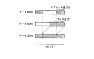
- bit field operation circuit A performs the bit field operation shown in FIG.
- data A2000 and data B2001 are an n-bit bit string input to the bitfield operation circuit A when the bitfield operation circuit A performs a bitfield operation
- data C2002 is a bitfield operation circuit. This is an n-bit bit string output from the bit field operation circuit A when A performs a bit field operation.
- bit field operation circuit A When an instruction designating data A2000, data B2001, offset amount 2010, and wide amount 2011 is input, the bit field operation circuit A is shifted to the left by the offset amount 2010 from the position of the least significant bit in the data A2000. In the data B2001, a bit field operation is performed to generate data C2002 in which a bit string having the number of bits indicated by the wide amount 2011 including the least significant bit is inserted.
- bit field operation circuit B performs the bit field operation shown in FIG.
- data A 2100 is an n-bit bit string input to the bit field operation circuit B when the bit field operation circuit B performs the bit field operation
- data B 2101 is data stored in the bit field operation circuit A by the bit field. This is an n-bit bit string output from the bit field operation circuit B when the operation is performed.
- the bit field operation circuit B When a command specifying data A2100, offset amount 2110, and shift amount 2111 is input, the bit field operation circuit B offsets the amount of offset in the data A2100 with respect to data obtained by logically shifting the data A2100 to the right by the shift amount.
- a bit field operation for generating data B2101 in which a bit string including the least significant bit of the number of bits indicated by 2110 is inserted is performed.
- an object of the present invention is to provide a data processing apparatus that can perform unpacking of packed data relatively efficiently.
- the data processing apparatus includes, from one instruction, information specifying a bit string storage area for storing a target bit string of N (N is an integer of 2 or more) bits, and an N-bit bit string.
- a decoder that reads information indicating a second bit range that does not include the second end bit in the bit string of bits, and outputs a decode signal corresponding to the read information; and when the decode signal is output from the decoder, In response to the decoded signal, an output bit string consisting of N bits based on the target bit string stored in the bit string storage area is generated and output.
- bit manipulation circuit wherein the bit manipulation circuit arranges a bit string having the same value as the bit string in the first bit range in the target bit string in the first bit range in the output bit string, and the bit manipulation circuit in the output bit string
- bit string having the same value as the bit string of the second bit range in the target bit string is arranged in a third bit range including the bit length of the second bit range, including the end bit of 2, and the first bit in the output bit string
- the output bit string is generated by arranging the same predetermined value in a portion that does not belong to either the bit range or the third bit range.
- the bit operation circuit that operates according to the decode signal decoded from one instruction includes the first bit range and the first bit range of the bit string stored in the bit string storage area.
- the data packed in the 2-bit range is unpacked and output so that a bit string having the same predetermined value is inserted between the first bit range and the second bit range.
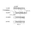
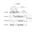
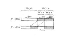
- FIG. 23 is a diagram showing a specific example of the data structure before the lower-end data unpacking process and the data structure after the lower-end data unpacking process in the lower-end data unpacking process which is an example of the data unpacking process. It is.
- the bottom-packed data unpacking process is a process of unpacking so that each of the plurality of bit strings that are data-packed is arranged on the least significant bit side of each bit string that is an integer multiple of the word unit. That is.
- data A 2300 is a 32-bit bit string before the unpacking data unpacking process, which is a 16-bit bit string composed of a 7-bit valid bit string 2301 and a 9-bit valid bit string 2302, and a 16-bit logic. It consists of an unnecessary bit string 2303 having a value “0”.
- Data B2310 is a 32-bit bit string after the lower-order data unpacking process, and the valid bit string 2301 is arranged at the least significant bit side position in the upper 16 bits, and the least significant bit side position in the lower 16 bits.
- the lower bit data unpacking process is performed so that the valid bit string 2302 is arranged in the data.
- extended bit string 2311 a part of the bit string 2311 (hereinafter referred to as “extended bit string 2311”).
- extended bit string 2311 a part of the bit string 2311 (hereinafter referred to as “extended bit string 2311”).
- extended bit string 2311 when handling as an unsigned integer, the extension bit string 2311 needs to be filled with the value “0”.
- the extension bit string 2311 is the most significant bit of the effective bit string 2302. Must be filled with values.
- first data unpacking process a first-stage data unpacking process that fills the extended bit string 2311 with a predetermined value. .
- first data unpacking process a first-stage data unpacking process that fills the extended bit string 2311 with a predetermined value. .
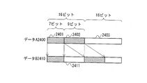
- FIG. 24 is a diagram illustrating a specific example of the data structure before the top-packed data unpacking process and the data structure after the top-packed data unpacking process in the top-packed data unpacking process that is an example of the data unpacking process. It is.
- the upper-packed data unpacking process is a process of unpacking so that each of the plurality of bit strings that are data-packed is arranged on the most significant bit side in each bit string that is an integer multiple of the word unit. That is.
- data A2400 is a 32-bit bit string before the upper-packed data unpacking process, and is a 16-bit bit string composed of a 7-bit valid bit string 2401 and a 9-bit valid bit string 2402, and a 16-bit logic. It consists of an unnecessary bit string 2403 having a value “0”.
- Data B2410 is a 32-bit bit string after the upper-packed data unpacking process, and the valid bit string 2401 is arranged at the most significant bit side position in the upper 16 bits, and the most significant bit side position in the lower 16 bits.
- the data has been subjected to the upper-packed data unpacking process so that the valid bit string 2402 is arranged in the.
- bit string 2411 the bit string 2411 portion (hereinafter, referred to as a bit string 2411) "Expanded bit string 2411") must be filled with the same predetermined value. That is, when handling as an unsigned integer, the extension bit string 2411 needs to be filled with the value “0”. When handling as a signed integer, the extension bit string 2411 is the most significant bit of the effective bit string 2402. Must be filled with values.
- the conventional bit field operation circuit A and the conventional bit field operation circuit B are referred to as a top-packed data unpacking process (hereinafter referred to as “second data unpacking process”) that fills the extended bit string 2411 with a predetermined value. ) Cannot be realized with one instruction. Therefore, in the conventional data processing apparatus, in order to realize the second data unpacking process, it is necessary to execute at least two instructions in combination.
- the number of instructions that can be executed per unit time is limited. Therefore, in the conventional data processing apparatus, it is desired that the first data unpacking process and the second data unpacking process, which are required to be executed by combining at least two instructions, are executed by one instruction. .
- the data processing apparatus 100 was developed for the purpose of providing a data processing apparatus capable of executing the first data unpacking process and the second data unpacking process with one instruction.
- the data processing apparatus 100 includes an instruction decoder, a register file, and a bit operation circuit.
- the bit operation circuit shifts data stored in the register file based on a decode signal output from the instruction decoder. Bit operations related to processing are performed.
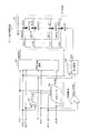
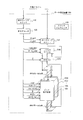
- FIG. 1 is a block diagram showing the main hardware configuration of the data processing apparatus 100.
- the data processing device 100 is, for example, a semiconductor integrated circuit including an instruction fetch unit 110, an instruction decoder 120, a load / store unit 130, a register file 140, a bit operation circuit 150, and a clock generator 160.
- the clock generator 160 has a function of generating and outputting, for example, a 100 MHz clock signal supplied to the instruction fetch unit 110, the instruction decoder 120, the load / store unit 130, the register file 140, and the bit operation circuit 150.
- the instruction fetch unit 110 is connected to the instruction decoder 120 and an external memory, and has the following two functions.
- Function 1 A function of reading one instruction of 4 bytes stored in the external memory in synchronization with a clock signal supplied from the clock generator 160 and outputting the read instruction to the instruction decoder 120.
- Function 2 A function in which the address used when reading an instruction from the external memory is incremented by 4 bytes with respect to the address used when reading the instruction from the external memory last time.
- FIG. 2 is a bit field configuration diagram of one instruction consisting of 4 bytes stored in the external memory.
- one instruction consisting of 4 bytes stored in the external memory has a 1-bit sign field 201, a 1-bit mask_dir field 202, a 1-bit operation field 203, and a 6-bit operation.
- An N field 204, a 5-bit width field 205, a 5-bit shift_len field 206, a 4-bit read_addr field 207, a 4-bit write_addr field 208, and a 5-bit other field 209 are configured.
- the instruction decoder 120 is connected to the instruction fetch unit 110, the load / store unit 130, the register file 140, and the bit operation circuit 150, and receives an instruction described in a predetermined format input from the instruction fetch unit 110 in advance. It has a function of decoding according to a predetermined algorithm.
- the instruction to be decoded by the instruction decoder 120 includes a load / store type instruction related to a load / store process performed using the load / store unit 130 and the register file 140, and a bit performed using the register file 140 and the bit operation circuit 150.
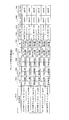
- FIG. 3 is a decode signal correspondence table 200 showing the correspondence between the bit operation type instruction to be decoded and the decode signal when the instruction decoder 120 decodes the bit operation type instruction.
- an instruction format 210 indicates an instruction format in a mnemonic format of a bit operation type instruction to be decoded.
- the bit manipulation type instructions include a shrnhN instruction in which the operation code is shrnhN (N is 8 or 16 or 32, and so on), a shrnlN instruction in which the operation code is shrnlN, a shrnlsN instruction in which the operation code is shrnlsN, and an operation code
- a shrnhN instruction with an extrhN operation a shrnlN instruction with an operation code extrlN
- an extrlsN instruction with an operation code extrlsN There are six types: an extrhN instruction with an extrhN operation, an extrlN instruction with an operation code extrlN, and an extrlsN instruction with an operation code extrlsN.
- These instructions include a register name B that specifies a destination register in the register file 140, a register name A that specifies a source register in the register file 140, and a shift_len that indicates a first bit length that is less than N. And the width indicating the second bit length that is less than N are used as operands.
- Sign 220, mask_dir 230, operation 240, N250, width 260, shift_len 270, read_addr 280, and write_addr 290 are decode signals output when the instruction decoder 120 decodes the bit operation type instruction.
- the sign 220 is a signal having a logical value “1” when the sixth character of the operation code is “s”, and a logical value “0” when the sixth character of the operation code is not “s”. It is output to the operation circuit 150.
- This sign 220 is a signal indicating whether the bit manipulation processing performed by the bit manipulation circuit 150 is a sign extension processing with a sign extension or a zero extension process without a sign extension.
- the sign 220 is decoded based on the sign field 201 in FIG.
- the mask_dir 230 has a logical value “0” when the fifth character of the operation code is “h”, and a logical value “1” when the fifth character of the operation code is not “h”, that is, “l”. , And is output to the bit operation circuit 150.
- the mask_dir 230 is a signal for specifying a bit string that is not subject to shift processing in the bit manipulation processing performed by the bit manipulation circuit 150. The bit string that is not subject to shift processing will be described later.
- the mask_dir 230 is decoded based on the mask_dir field 202 in FIG.
- the operation 240 is a logical value “0” when the first to fourth characters of the operation code are “shrn”, and when the first to fourth characters of the operation code are not “shrn”, that is, “extr”. In some cases, the signal has a logical value “1” and is output to the bit operation circuit 150.
- the operation 240 is a signal for specifying a shift direction of a bit string that is a shift process target with respect to a bit string that is not a shift process target in the bit operation process performed by the bit operation circuit 150. The bit string to be shifted is described later.
- the operation 240 is decoded based on the operation field 203 in FIG.
- N250 is a 6-bit signal indicating the number N included in the operation code in binary, and is output to the bit operation circuit 150. This N250 is a signal indicating the bit length of the bit string to be subjected to bit manipulation processing performed by the bit manipulation circuit 150.
- N250 is decoded based on the N field 204 in FIG.
- Width 260 is a 5-bit signal indicating the value of the operand width in binary, and is output to the bit operation circuit 150.
- the width 260 is a signal indicating the bit length of the bit string to be shifted in the bit manipulation processing performed by the bit manipulation circuit 150.
- the width 260 is decoded based on the width field 205 in FIG.
- Shift_len 270 is a 5-bit signal indicating the value of the operand shift_len in binary, and is output to the bit operation circuit 150.
- This shift_len 270 is a signal indicating the shift amount of the bit string to be subjected to the bit operation processing performed by the bit operation circuit 150.
- shift_len 270 is decoded based on the shift_len field 206 in FIG.
- Read_addr 280 is a signal (addrA) designated by the operand A and indicating the 4-bit address of the source register in the register file 140, and is output to the register file 140. This read_addr 280 is decoded based on the read_addr field 207 in FIG.
- the write_addr 290 is a signal (addrB) designated by the operand B and indicating the 4-bit address of the source register in the register file 140, and is output to the register file 140. This write_addr 290 is decoded based on the write_addr field 208 in FIG.
- the load store unit 130 is connected to the instruction decoder 120, the register file 140, and an external memory, and has the following two functions.
- Function 1 When the signal ld_addr indicating the address of the external memory, which is output when the load / store type instruction is decoded, is input from the instruction decoder 120, the ld_addr is synchronized with the clock signal supplied from the clock generator 160. A function of reading out 4 bytes of data in the storage area in the external memory designated by the address indicated by the external memory and outputting the data to the register file 140.
- Function 2 When the signal st_addr indicating the address of the external memory, which is output when the load / store type instruction is decoded, is input from the instruction decoder 120, the register is synchronized with the clock signal supplied from the clock generator 160. A function of writing 4-byte data input from the file 140 into a storage area in the external memory specified by an address indicated by st_addr.
- the register file 140 is connected to the instruction decoder 120, the load / store unit 130, and the bit operation circuit 150, and has 16 general-purpose registers each consisting of 4 bytes, and has the following two functions.
- Function 1 A function of outputting 4-byte data stored in the source register specified by read_addr in synchronization with the clock signal supplied from the clock generator 160 when read_addr is input from the instruction decoder 120.
- the bit operation circuit 150 is connected to the instruction decoder 120 and the register file 140.
- the bit operation circuit 150 performs processing according to the decode signal input from the instruction decoder 120 on the data dataA input from the register file 140 to obtain the data dataB. It has a function to generate and output.
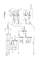
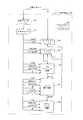
- FIG. 4 is a circuit configuration diagram showing a circuit configuration of the bit operation circuit 150.
- the bit operation circuit 150 includes an exclusive OR gate 310, a left / right shifter 320, a sign extension circuit 330, an adder 340, a mask data generation circuit 350, and a first bit selector 360.
- the exclusive OR gate 310 is a two-input exclusive OR circuit connected to the signal line of the decode signal mask_dir, the signal line of the decode signal operation, and the left and right shifters 320.
- the exclusive OR gate 310 outputs a 1-bit signal shift_dir indicating the shift direction of the left and right shifters 320 to the left and right shifters 320 when two decode signals of mask_dir and operation are input.
- the left / right shifter 320 is a left / right barrel shifter connected to the signal line of the decode signal sign, the signal line of the decode signal shift_len, the exclusive OR gate 310, the signal line of the input data dataA, and the sign extension circuit 330. Based on sign, shift_len, and shift_dir, the input data dataA is shifted and output data dataAA is output.
- Shift_dir A signal that controls whether the shift direction is right (lower bit side) or left (upper bit side).
- the left and right shifter 320 shifts to the right when shift_dir is a logical value “1”, and shifts to the left when shift_dir is a logical value “0”.
- Shift_len Control signal indicating the shift amount.
- the left / right shifter 320 shifts to the right or left by the shift amount indicated by shift_len.
- Sign A signal that controls whether the shift method at the time of right shift is right shift with sign extension, that is, arithmetic shift, or right shift without sign extension, that is, logical shift.
- the left / right shifter 320 performs a right shift with sign extension when sign is a logical value “1” during right shift, and does not accompany a sign extension when sign is a logical value “0” during right shift. Shift right.
- the sign extension circuit 330 includes a decode signal sign signal line, a decode signal mask_dir signal line, a decode signal operation signal line, a decode signal N signal line, a decode signal width signal line, a left / right shifter 320, and a first bit selector 360. Based on the control signals sign, mask_dir, operation, N, and width, a copy of the signal at the predetermined bit position or the logical value “0” at the position of the predetermined bit string in the input data dataAA Is inserted and the output data dataAAA is output.
- FIG. 5 is a circuit configuration diagram showing a circuit configuration of the sign extension circuit 330.
- the sign extension circuit 330 includes a subtractor 410, a first selector 420, a second selector 430, a third selector 440, a decoder 450, and a second bit selector 460.
- the subtractor 410 is connected to the signal line of the decode signal width, the signal line of the decode signal N, and the first selector 420, and subtracts the value of width from the value of N and outputs a 6-bit signal N-width.
- the first selector 420 is a 6-bit 2-input 1-output selector connected to the signal line of the decode signal mask_dir, the signal line of the decode signal width, and the subtractor 410, and the control signal mask_dir is a logical value “ When “1”, width is selected, and when mask_dir is a logical value “0”, N-width is selected, and a 6-bit signal sign_offset is output.
- This sign_offset is a signal indicating the position of the predetermined bit in an N-bit bit string to be subjected to bit manipulation processing.
- the second selector 430 is a 1-bit 32-input 1-output selector connected to the signal line of the input data dataAA, the first selector 420, and the third selector 440. From the input data dataAAA, which is a 32-bit bit string, , A bit at a position indicated by the control signal sign_offset is selected and a 1-bit signal sign_data is output.
- the third selector 440 is a 1-bit 2-input 1-output selector connected to the signal line of the decode signal sign, the second selector 430, and the second bit selector 460, and the control signal sign is a logical value “ When “1”, sign_data is selected, and when sign is a logical value “0”, a logical value “0” is selected, and a 1-bit signal ext_data is output.
- the decoder 450 is a decoder connected to the signal line of the decode signal operation, the signal line of the decode signal mask_dir, the signal line of the decode signal width, the signal line of the decode signal N, and the second bit selector 460, and is inputted. From operation, mask_dir, width, and N, it has a function of decoding a 32-bit ext_mask signal.
- FIG. 6 is a truth table for decoding performed by the decoder 450.
- operation 510, mask_dir 520, and width 530 are signals input to the decoder 450, and ext_mask (Nbit) 540 is a bit string composed of the lower N bits of the 32-bit decode signal ext_mask.
- ext_mask (Nbit) 540 is a bit string composed of the lower N bits of the 32-bit decode signal ext_mask.
- the value of a portion excluding the lower N bits of the ext_mask consisting of 32 bits is a don't care value (not shown).
- the decoder 450 When operation, mask_dir, width, and N are input, the decoder 450 outputs ext_mask according to the truth table shown in FIG.
- the second bit selector 460 is connected to a signal line of input data dataAA, a third selector 440, a decoder 450, and a first bit selector 360 (see FIG. 4), and includes 32 2-input 1-output selectors. On the other hand, it has a function of generating dataAAA by inserting a bit of ext_data at a bit position specified by ext_mask.
- Each of the selectors constituting the second bit selector 460 has a function of selecting and outputting either the corresponding dataAA bit or ext_data using each bit of ext_mask as a control signal.
- the adder 340 is connected to the signal line of the decode signal width, the signal line of the decode signal shift_len, and the mask data generation circuit 350, adds the value of width and the value of shift_len, and outputs mask_width that is a 6-bit signal. It has the function to do.
- the mask data generation circuit 350 is a decoder connected to the signal line of the decode signal mask_dir, the signal line of the decode signal N, the adder 340, and the first bit selector 360, and receives the mask_dir, N, and mask_width input thereto. , Has a function of decoding a 32-bit mask signal.
- FIG. 7 is a truth table of decoding performed by the mask data generation circuit 350.
- mask_dir 610 and mask_width 620 are signals input to the mask data generation circuit 350
- mask (Nbit) 630 is a bit string composed of the lower N bits of the 32-bit decode signal mask. The value of the portion excluding the lower N bits in the 32-bit mask is a don't care value (not shown).
- the mask data generation circuit 350 When mask_dir, mask_width, and N are input, the mask data generation circuit 350 outputs a mask according to the truth table shown in FIG.
- the first bit selector 360 is connected to the signal line of the input data dataA, the sign extension circuit 330, the mask data generation circuit 350, and the signal line of the output data dataB, and includes 32 2-input 1-output selectors. It has a function of generating dataB by inserting dataAAA data at the bit position specified by mask.
- Each of these selectors has a function of selecting and outputting either the corresponding dataA bit or the corresponding dataAAA bit using each bit of the mask as a control signal.
- FIG. 8 is a data configuration diagram showing a configuration of data used and generated by the bit operation circuit 150 when the instruction decoder 120 decodes the shrnhN instruction.
- dataA700 is a bit string of the lower N bits of the 32-bit input data output from the register file 140 in the same cycle as the clock cycle in which the instruction decoder 120 outputs the decode signal.
- the dataAA 710 is a bit string of the lower N bits of the 32-bit data dataAA output from the left / right shifter 320 corresponding to dataA input from the register file 140.
- the dataAAA 720 is a bit string of the lower N bits of the 32-bit data dataAAA output from the sign extension circuit 330 corresponding to the dataAA input from the left / right shifter 320.
- dataB 730 is a bit string of the lower N bits of 32-bit data dataB output from the first bit selector 360 corresponding to dataAAA input from the sign extension circuit 330.
- the width 740 is a bit length specified by the decode signal width input from the instruction decoder 120.
- shift_len 750 is a shift amount specified by the decode signal shift_len input from the instruction decoder 120.
- the exclusive OR gate 310 When the decode signal corresponding to the shrnhN instruction is input from the instruction decoder 120, the exclusive OR gate 310 (see FIG. 4) outputs shift_dir having a logical value “0” to the left and right shifters 320. Then, the left and right shifter 320 shifts dataA700 leftward by the shift amount specified by shift_len750 and outputs dataAA710.
- the decoder 450 when the decoder 450 (see FIG. 5) receives a decode signal corresponding to the shrnhN instruction from the instruction decoder 120, the decoder 450 (see FIG. 5) outputs an ext_mask whose lower N bits are all logical values “0” to the second bit selector 460. Then, the second bit selector 460 outputs dataAA710 as it is as dataAAA720.
- the adder 340 (see FIG. 4) adds the value of width 740 and the value of shift_len 750, and outputs mask_width. Then, the mask data generating circuit 350 has a logical value “1” for the bit string including the least significant bit indicated by the value of mask_width in the lower N bits, and a logical value “0” for the other bits in the lower N bits. “1” is output to the first bit selector 360.
- the first bit selector 360 selects the bit string including the least significant bit of the bit width of the sum of the width 740 value and the shift_len 750 value from the dataAAA 720, selects the other bits from the dataA700, and sets it as dataB730. Output.
- the bit manipulation circuit 150 shifts the bit string including the least significant bit of the bit length specified by the width 740 from the dataA 700 by the shift amount specified by the shift_len 750.
- the bit string dataB730 is generated and output by shifting and not shifting the bit string including the most significant bit of the bit length specified by the value of N ⁇ (width 740 + shift_len 750).
- FIG. 9 is a data configuration diagram showing a configuration of data used and generated by the bit operation circuit 150 when the instruction decoder 120 decodes the shrnlN instruction.
- dataA800, dataAA810, dataAAA820, dataB830, width840 and shift_len850 are the same as dataA700, dataAA710, dataAAA720, dataB730, width740 and shift_len750 in FIG. 8, respectively. Therefore, these descriptions are omitted here.
- the exclusive OR gate 310 When the decode signal corresponding to the shrnlN instruction is input from the instruction decoder 120, the exclusive OR gate 310 outputs shift_dir having a logical value “1” to the left and right shifters 320. Then, the left / right shifter 320 shifts dataA800 to the right by the shift amount specified by shift_len850 and outputs dataAA810.
- a logical value “0” is inserted into the zero extension area 860 in FIG. 9.
- the decoder 450 when the decode signal corresponding to the shrnlN instruction is input from the instruction decoder 120, the decoder 450 outputs an ext_mask whose lower N bits are all logical values “0” to the second bit selector 460. Then, the second bit selector 460 outputs dataAA810 as it is as dataAAA820.
- the adder 340 adds the value of width 840 and the value of shift_len 850, and outputs mask_width. Then, the mask data generation circuit 350 has a bit string including the least significant bit of the bit length specified by the value of N ⁇ (width 840 + shift_len 850) out of the lower N bits as the logical value “1” and those of the lower N bits. A mask in which the other bits have a logical value “0” is output to the first bit selector 360.
- the first bit selector 360 selects the bit string including the most significant bit of the bit width of the sum of the value of width 840 and the value of shift_len 850 from dataAAA 820 and selects other bits from dataA800 as dataB 830. Output.
- the bit operation circuit 150 encodes a bit string including the most significant bit of the bit length specified by width 840 from the dataA 800 by the shift amount specified by shift_len850.
- the bit string dataB830 is generated and output by shifting right without extension and not shifting the bit string including the least significant bit of the bit length specified by the value of N ⁇ (width 840 + shift_len 850).
- FIG. 10 is a data configuration diagram showing a configuration of data used and generated by the bit operation circuit 150 when the instruction decoder 120 decodes the shrnlsN instruction.
- dataA900, dataAA910, dataAAA920, dataB930, width940 and shift_len950 are the same as dataA700, dataAA710, dataAAA720, dataB730, width740 and shift_len750 in FIG. 8, respectively. Therefore, these descriptions are omitted here.
- the exclusive OR gate 310 When the decode signal corresponding to the shrnlsN instruction is input from the instruction decoder 120, the exclusive OR gate 310 outputs shift_dir having a logical value “1” to the left and right shifters 320. Then, the left / right shifter 320 shifts dataA800 to the right by the shift amount specified by shift_len850, and outputs dataAA810.
- the shift performed by the left / right shifter 320 is accompanied by sign extension, the most significant bit of dataA900 is sign-extended in the sign extension area 960 in FIG.
- the decoder 450 when the decode signal corresponding to the shrnlsN instruction is input from the instruction decoder 120, the decoder 450 outputs ext_mask whose lower N bits are all logical values “0” to the second bit selector 460. Then, the second bit selector 460 outputs dataAA910 as it is as dataAAA920.
- the adder 340 adds the value of width 940 and the value of shift_len 950, and outputs mask_width. Then, the mask data generation circuit 350 has a bit string including the least significant bit of the bit length specified by the value of N ⁇ (width 940 + shift_len 950) among the lower N bits as the logical value “1” and those among the lower N bits. A mask in which the other bits have a logical value “0” is output to the first bit selector 360.
- the first bit selector 360 selects the bit string including the most significant bit of the bit width of the sum of the width 940 value and the shift_len 950 value from the dataAAA 920, selects the other bits from the dataA900, and sets it as the dataB930. Output.
- the bit manipulation circuit 150 encodes the bit string including the most significant bit having the bit length specified by the width 940 from the dataA 900 by the shift amount specified by the shift_len 950.
- the bit string dataB830 is generated and output by shifting to the right with extension and not shifting the bit string including the least significant bit of the bit length specified by the value of N ⁇ (width 940 + shift_len 950).
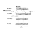
- FIG. 11 is a data configuration diagram showing a configuration of data used and generated by the bit operation circuit 150 when the instruction decoder 120 decodes the extrhN instruction.
- dataA1000, dataAA1010, dataAAA1020, dataB1030, width1040, and shift_len1050 are the same as dataA700, dataAA710, dataAAA720, dataB730, width740, and shift_len750 in FIG. 8, respectively. Therefore, these descriptions are omitted here.
- the exclusive OR gate 310 When the decode signal corresponding to the extrhN instruction is input from the instruction decoder 120, the exclusive OR gate 310 outputs shift_dir having a logical value “1” to the left and right shifters 320. Then, the left / right shifter 320 shifts dataA1000 to the right by the shift amount specified by shift_len1050, and outputs dataAA1010.
- shift_dir having a logical value “1”
- shift_len1050 the shift amount specified by shift_len1050
- the third selector 440 outputs the logical value “0” as ext_data because the sign input from the instruction decoder 120 is the logical value “0”.
- the decoder 450 receives the decode signal corresponding to the extrhN instruction from the instruction decoder 120, the bit string including the least significant bit having the bit length specified by the value of width 1040 among the lower N bits is converted into a logical value “ 1 "is output, and ext_mask in which the other bits of the lower N bits have the logical value" 0 "is output.
- the second bit selector 460 generates a bit string dataAAA1020 by selecting a bit string including the least significant bit of the bit length specified by width 1040 from dataAA1010 and selecting a logical value “0” for the other bits. And output. Therefore, the second zero extension area 1070 in FIG. 11 has a logical value “0”.
- the adder 340 adds the value of width 1040 and the value of shift_len 1050, and outputs mask_width. Then, the mask data generation circuit 350 has the bit string including the least significant bit of the bit length specified by the value of width 1040 + shift_len1050 among the lower N bits as the logical value “1”, and other bits out of the lower N bits as the bit string. A mask having a logical value “0” is output to the first bit selector 360.
- the first bit selector 360 selects the bit string including the least significant bit of the bit width of the sum of the width 1040 value and the shift_len 1050 value from the dataAAA 1020, selects the other bits from the dataA1000, and sets it as the dataB1030. Output.
- the bit manipulation circuit 150 converts the bit string including the least significant bit having the bit length specified by the value of width 1040 + shift_len 1050 from the dataA1000 to the shift amount specified by the shift_len 1050.
- the bit string including the most significant bit of the bit length specified by the value of N ⁇ (width 1040 + shift_len 1050) is not shifted, and the bit string dataB1030 is generated and output.
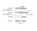
- FIG. 12 is a data configuration diagram showing a configuration of data used and generated by the bit operation circuit 150 when the instruction decoder 120 decodes the extrlN instruction.
- dataA1100, dataAA1110, dataAAA1120, dataB1130, width1140, and shift_len1150 are the same as dataA700, dataAA710, dataAAA720, dataB730, width740, and shift_len750 in FIG. 8, respectively. Therefore, these descriptions are omitted here.
- the exclusive OR gate 310 When the decode signal corresponding to the extrlN instruction is input from the instruction decoder 120, the exclusive OR gate 310 (see FIG. 4) outputs the shift_dir having the logical value “0” to the left and right shifters 320. Then, the left / right shifter 320 shifts dataA1100 leftward by the shift amount specified by shift_len1150, and outputs dataAA1110.
- the third selector 440 outputs the logical value “0” as ext_data because the sign input from the instruction decoder 120 is the logical value “0”.
- the decoder 450 converts the bit string including the most significant bit having the bit length specified by the value of width 1040 among the lower N bits to the logical value “ 1 "is output, and ext_mask in which the other bits of the lower N bits have the logical value" 0 "is output.
- the second bit selector 460 generates a bit string dataAAA1120 by selecting a bit string including the most significant bit having a bit length specified by width 1140 from dataAA1110 and selecting a logical value “0” for the other bits. And output. Therefore, the first zero extension region 1160 in FIG. 12 has a logical value “0”.
- the adder 340 adds the value of width 1140 and the value of shift_len 1150, and outputs mask_width. Then, the mask data generation circuit 350 has the bit string including the most significant bit of the bit length specified by the value of width 1140 + shift_len 1150 among the lower N bits as the logical value “1”, and other bits out of the lower N bits as the bit string. A mask having a logical value “0” is output to the first bit selector 360.
- the first bit selector 360 selects a bit string including the most significant bit of the bit width of the sum of the value of width 1140 and the value of shift_len 1150 from dataAAA 1120 and selects other bits from dataA1100 as dataB1130. Output.
- the bit manipulation circuit 150 converts the bit string including the most significant bit having the bit length specified by the value of width1140 + shift_len1150 from the dataA 1100 to the shift amount specified by the shift_len1150.
- the bit string including the least significant bit of the bit length specified by the value of N ⁇ (width1140 + shift_len1150) is not shifted, and the logical value of the portion of the second zero extension area 1170 in FIG.
- the bit string dataB1130 is generated and output.
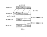
- FIG. 13 is a data configuration diagram showing a configuration of data used and generated by the bit operation circuit 150 when the instruction decoder 120 decodes the extrlsN instruction.
- dataA1200, dataAA1210, dataAAA1220, dataB1230, width1240, and shift_len1250 are the same as dataA700, dataAA710, dataAAA720, dataB730, width740, and shift_len750 in FIG. 8, respectively. Therefore, these descriptions are omitted here.
- the exclusive OR gate 310 When the decode signal corresponding to the extrlN instruction is input from the instruction decoder 120, the exclusive OR gate 310 (see FIG. 4) outputs the shift_dir having the logical value “0” to the left and right shifters 320. Then, the left / right shifter 320 shifts dataA1100 leftward by the shift amount specified by shift_len1150, and outputs dataAA1110.
- the first selector 420 selects the N-width output from the subtractor 410 and outputs it as sign_offset. Then, the second selector 430 outputs the signal of the N-width bit in dataAA1210 as sign_data. Furthermore, since the sign input from the instruction decoder 120 is the logical value “1”, the third selector 440 outputs the N-width bit signal of the dataAA1210 as ext_data.
- the bit string including the most significant bit having the bit length specified by the value of width 1040 among the lower N bits is converted into a logical value “ 1 "is output, and ext_mask in which bits other than those of the lower N bits have a logical value" 0 "is output.
- the second bit selector 460 selects a bit string including the most significant bit of the bit length specified by width 1140 from dataAA1210, and selects the N-width bit signal of dataAA1210 for other bits.
- the bit string dataAAA1120 is generated and output. Therefore, the first code extension area 1260 in FIG. 13 is the logical value of the N-width bit in dataAA1210.
- the adder 340 adds the value of width 1240 and the value of shift_len 1250, and outputs mask_width. Then, the mask data generation circuit 350 has a logical value “1” for the bit string including the most significant bit of the bit length specified by the value of width 1240 + shift_len 1250 among the lower N bits, and bits other than those of the lower N bits.
- the mask that is the logical value of the N-width bit in dataAA1210 is output to the first bit selector 360.
- the first bit selector 360 selects a bit string including the most significant bit of the bit width of the sum of the width 1240 value and the shift_len 1250 value from the dataAAA 1220, selects other bits from the dataA1200, and sets it as dataB1230. Output.
- the bit manipulation circuit 150 converts the bit string including the most significant bit having the bit length specified by the value of width 1240 + shift_len 1250 from the dataA 1200 to the shift amount specified by the shift_len 1250.
- the bit string including the least significant bit of the bit length specified by the value of N ⁇ (width1240 + shift_len1250) is not shifted, and the second code extension area 1270 in FIG. By duplicating the -width bit signal, the bit string dataB1230 is generated and output.
- a bit operation process is a characteristic operation performed by the data processing apparatus 100. Hereinafter, this bit operation processing will be described with reference to the drawings.
- the bit manipulation process is a process performed by the instruction decoder 120, the register file 140, and the bit manipulation circuit 150 in cooperation when the instruction fetch unit 110 (see FIG. 1) reads a bit manipulation type instruction from the external memory. .
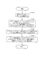
- FIG. 14 is a flowchart of bit operation processing performed by the data processing apparatus 100.
- Bit operation processing starts when the instruction fetch unit 110 reads a bit operation type instruction from the external memory.
- the instruction fetch unit 110 When the instruction fetch unit 110 reads the bit operation type instruction from the external memory, the instruction fetch unit 110 outputs the read bit operation type instruction to the instruction decoder 120. Then, the instruction decoder 120 starts decoding the input bit operation type instruction (step S1310).
- the instruction decoder 120 When the instruction decoder 120 decodes the bit operation type instruction, the instruction decoder 120 outputs the decode signal read_addr and the decode signal write_addr to the register file 140, and decodes the sign signal, the decode signal mask_dir, the decode signal operation, the decode signal N, the decode signal width, and the decode.
- the signal shift_len is output to the bit operation circuit 150 (step S1320).
- the register file 140 When the read_addr is input from the instruction decoder 120, the register file 140 outputs the data stored in the register specified by the read_addr (step S1330).
- the bit operation circuit 150 performs bit operations based on sign, mask_dir, operation, N, width, and shift_len, which are input from the instruction decoder 120, on the data input from the register file 140, and performs bit operations.
- the data generated by the execution is written in the register specified by write_addr in the register file 140 (step S1340).
- step S1340 the data processing apparatus 100 ends the bit operation process.
- the data processing apparatus 100 can perform the top unpacking process with one instruction.
- the upper-order unpacking process is performed on the 32-bit data stored in the first register in the register file 140, and the execution result is displayed in the register file 140. It is an example in the case of storing in the second register.
- FIG. 15 is a data configuration diagram showing a configuration of data used and generated by the bit operation circuit 150 in the illustrated specific example.
- dataA1400 is 32-bit data stored in the first register in the register file 140, and is a 16-bit bit string composed of a 7-bit effective bit string 1401 and a 9-bit effective bit string 1402. , An unnecessary bit string 1403 having a 16-bit logical value “0”.
- the dataAA 1410 is a 32-bit bit string output from the left / right shifter 320 (see FIG. 4) corresponding to the dataA 1400 input from the register file 140.
- the dataAAA 1420 is a 32-bit bit string output from the sign extension circuit 330 corresponding to the dataAA 1410 input from the left / right shifter 320.
- dataB 1430 is a 32-bit bit string output from the first bit selector 360 corresponding to dataAAA input from the sign extension circuit 330.
- the width 1440 is a bit length specified by the decode signal width input from the instruction decoder 120, and its value is 16 here as described later.
- shift_len 1450 is a shift amount specified by the decode signal shift_len input from the instruction decoder 120, and its value is 9 as described later.
- the instruction decoder 120 informs the instruction decoder 120 that the opcode is extrh32, the operand B is the register name of the second register, and the operand A is the register name of the first register.
- the operand shift_len is 9 which is the bit length of the effective bit string 1402, and the instruction whose operand width is 16 which is the unit bit length of the unpacked data is input. A bit operation process that is an upper unpacking process is started.
- the instruction decoder 120 When the bit manipulation process is started, the instruction decoder 120 outputs a decode signal to the bit manipulation circuit 150, and the register file 140 outputs dataA 1400 stored in the first register to the bit manipulation circuit 150.
- the left / right shifter 320 (see FIG. 4) shifts dataA1400 in the right direction without sign extension for 9 bits specified by shift_len1450, dataAA1410 is output.
- the bit string including the least significant bit having a bit length of 16 bits specified by the width 1040 has a logical value “1”, and other bits have a logical value “0”.
- Output ext_mask the second bit selector 460 generates a bit string dataAAA1420 by selecting a 16-bit bit string including the least significant bit from dataAA1410 and selecting a logical value “0” for the other bits.
- a mask of “0” is output to the first bit selector 360.
- the first bit selector 360 selects a bit string including the least significant bit having a bit width of 25 bits from the dataAAA 1420, selects other bits from the dataA1400, and outputs them as dataB1430.
- the register file 140 stores dataB 1430 output from the bit operation circuit 150 in the second register.
- the data processing apparatus 100 converts the 7-bit effective bit string 1401 and the 9-bit effective bit string 1402 into the 16-bit bit string in the upper 16 bits of the data stored in the first register.
- the top unpacking processing that is arranged on the most significant bit side and stored in the second register can be executed with one instruction.
- a data processing device 1500 obtained by modifying a part of the data processing device 100 according to the first embodiment will be described as an embodiment of the data processing device according to the present invention.
- the data processing device 1500 includes a plurality of bit manipulation circuits similar to the bit manipulation circuit 150 in the first embodiment, and executes the plurality of bit manipulation circuits in parallel, thereby performing SIMD (Single Instruction Multi Multi Data) type data processing. It can be performed.
- SIMD Single Instruction Multi Multi Data
- FIG. 16 is a block diagram showing the main hardware configuration of the data processing device 1500.
- the instruction decoder 120 is changed to the instruction decoder 1520
- the register file 140 is changed to the register file 1540
- the aligner 1570 is changed.
- the number of bit manipulation circuits provided is changed to be eight of the first bit manipulation circuit 1551 to the eighth bit manipulation circuit 1558.
- the instruction decoder 1520 is modified from the instruction decoder 120 according to the first embodiment so that a function of decoding a SIMD type bit manipulation type instruction is added.
- FIG. 17 is a decode signal correspondence table 1600 showing the correspondence between SIMD type bit operation type instructions to be decoded and decode signals when the instruction decoder 120 decodes SIMD type bit operation type instructions.
- an instruction format 1610 indicates an instruction format in a mnemonic format of a SIMD type bit manipulation type instruction to be decoded.
- the opcode is shrnhNxM (where N is either 8 or 16 or 32, M is either 2 or 4 or 8, and so on) and shrnlNxM where the opcode is shrnlNxM
- shrnlNxM There are six types of instructions: a shrnlsNxM instruction whose operation code is shrnlsNxM, an extrhNxM instruction whose operation code is extrhNxM, an extrlNxM instruction whose operation code is extrlNxM, and an extrlsNxM instruction whose operation code is extrlsNxM.
- These instructions include a register name B that designates a destination register in the register file 1540, a register name A that designates a source register in the register file 1540, and a shift_len that indicates a first bit length that is less than N. And the width indicating the second bit length that is less than N are used as operands.
- Sign 1620, mask_dir 1630, operation 1640, N1650, M1655, width 1660, shift_len 1670, read_addr 1680, and write_addr 1690 are decode signals output when the instruction decoder 1520 decodes the bit operation type instruction.
- sign 1620, mask_dir 1630, operation 1640, N1650, width 1660, shift_len 1670, read_addr 1680, and write_addr 1690 are sign 220, mask_dir 230, operation 240, and N250 in the first embodiment, respectively.
- Width 260, shift_len 270, read_addr 280, and write_addr 290 are omitted here.
- M1655 is a 4-bit signal indicating the number M included in the operation code in binary, and is output to the register file 1540.
- M1655 is a signal indicating the number of registers to be read or written when the register file 1540 reads or writes data.
- the register file 1540 is modified from the register file 140 according to the first embodiment so that the bit length of each of the 16 general-purpose registers is 4 bytes to 8 bytes.
- the aligner 1570 is connected to the instruction decoder 120, the register file 1540, and the first bit operation circuit 1551 to the eighth bit operation circuit 1558, and has the following six functions.
- Function 1 When M1655 is input from the instruction decoder 1520, when M1655 indicates “2” and a 64-bit bit string is input from the register file 1540, it consists of the upper 32 bits of the input bit string. A function of outputting a bit string to the first bit manipulation circuit 1551 and outputting a bit string consisting of the lower 32 bits of the input bit string to the second bit manipulation circuit 1552.
- Function 2 When M1655 is input from the instruction decoder 1520, when M1655 indicates “2”, a 32-bit bit string (hereinafter referred to as bit string A) and the second bit are output from the first bit operation circuit 1551.
- bit string B When a 32-bit bit string (hereinafter referred to as bit string B) is input from the operation circuit 1552, a 64-bit bit string having the bit string A on the upper side and the bit string B on the lower side is generated and sent to the register file 1540. Function to output.
- Function 3 When M1655 is input from the instruction decoder 1520, when M1655 indicates “4” and a 64-bit bit string is input from the register file 1540, the most significant 16 bits of the input bit string are used.
- the bit string is expanded to the upper side so as to become a 32-bit bit string and output to the first bit manipulation circuit 1551, and the second highest 16-bit bit string in the input bit string becomes a 32-bit bit string.
- the bit is extended to the upper side and output to the second bit manipulation circuit 1552, and the third bit manipulation circuit is bit-extended to the upper side so that the third highest 16-bit bit string becomes a 32-bit bit string.
- bit extension is realized, for example, by inserting a logical value “0” in the part to be extended.
- bit string C 16-bit bit string
- bit string E 16-bit bit string from the third bit operation circuit 1553
- bit string F 16-bit bit string from the fourth bit operation circuit 1554
- Function 5 When M1655 is input from the instruction decoder 1520, when M1655 indicates “8” and a 64-bit bit string is input from the register file 1540, the most significant 18 bits of the input bit string are The bit string is expanded to the upper side so as to become a 32-bit bit string and output to the first bit manipulation circuit 1551, and the bit string consisting of the second most significant 8 bits of the input bit string becomes a 32-bit bit string. In this way, the bit is expanded to the upper side and output to the second bit manipulation circuit 1552, and the third bit manipulation circuit is bit-expanded to the upper side so that the third highest bit string becomes a 32-bit bit string.
- the upper 4 bits of the upper 8-bit bit string becomes a 32-bit bit string
- the bit is extended to the fourth bit manipulation circuit 1554, and the bit string consisting of the fifth most significant 8 bits is bit-expanded so as to be a 32-bit bit string and output to the fifth bit manipulation circuit 1555.
- the sixth higher-order bit string consisting of the upper 8 bits is bit-expanded to the upper side so as to become a 32-bit bit string and output to the sixth bit manipulation circuit 1556
- the seventh higher-order bit string consisting of the upper 8 bits is 32 bits
- the bit is expanded to the upper side so as to be a bit string and output to the seventh bit manipulation circuit 1557
- the bit string consisting of the least significant 8 bits is bit-expanded to the upper side to become a 32-bit bit string. Function to output to the circuit 1554.
- the bit extension is realized, for example, by inserting a logical value “0” in the part to be extended.
- bit string G When M1655 is input from the instruction decoder 1520, when M1655 indicates “8”, an 8-bit bit string (hereinafter referred to as a bit string G) and a second bit from the first bit operation circuit 1551.
- bit string M The seventh bit manipulation circuit 1557, the 8-bit bit string (hereinafter referred to as bit string M), and the eighth bit manipulation circuit.
- bit string N When an 8-bit bit string (hereinafter referred to as bit string N) is input from 558, the bit string G, bit string H, bit string I, bit string J, bit string K, bit string L, bit string M, bit string N are sequentially input from the upper side.
- First bit operation circuit 1551 to eighth bit operation circuit 1558 each have the same function and configuration as bit operation circuit 150 in the first embodiment, and are connected to instruction decoder 1520 and aligner 1570, respectively.
- the decode signals from the instruction decoder 1520 that are common to each other are input.
- the data processing device 1500 having the above configuration performs the same processing as the bit manipulation processing performed by the data processing device 100 according to the first embodiment in parallel with the data stored in the register of the register file 1540 with one instruction. Can be executed. That is, so-called SIMD type bit manipulation processing can be performed.
- SIMD type bit manipulation processing can be performed.
- this data processing device 1700 when the instruction decoder decodes one of the instructions whose operation codes are extrhN, extrlN, and extrlsN (hereinafter, these instructions are referred to as “expansion instructions”), the data decoder 1700 reads the data from the register file. The output data is pre-unpacked and then input to the bit manipulation circuit, and the instruction decoder has instructions whose opcodes are shrnhN, shrnlN, and shrnlsN (hereinafter these instructions are referred to as “shrink instructions”). .) Is decoded, post-packing processing is performed on the data output from the bit manipulation circuit, and then output to the register file.
- the pre-unpacking process is a process of extending the bit length to 0 extension or sign extension in the bit string to be unpacked, and the post-packing process stores an unnecessary bit string in the bit string after the packing process. This refers to processing that invalidates the data in the part that is being processed.
- FIG. 18 is a block diagram showing the main hardware configuration of the data processing apparatus 1700.
- the data processing device 1700 is modified from the data processing device 100 according to the first embodiment so that a pre-pack circuit 1710 and a post-pack circuit 1720 are added.
- a pre-unpack circuit 1710 is connected to an instruction decoder 120, a register file 140, and a bit operation circuit 150, and has the following four pre-pack functions.
- Pre-unpack function 1 When the instruction decoder 120 decodes the decompression instruction, when the logical value of the decode signal sign input from the instruction decoder 120 is “0” and the logical value of the decode signal mask_dir is “0”, For the lower N bits of the 32-bit bit string input from the register file 140, the bit string including the least significant bit having a bit length of N / 2 is shifted N / 2 bits to the left, A function of inserting and outputting a bit string consisting of a logical value “0” in a bit string portion including the least significant bit having a bit length of N / 2.
- Pre-unpack function 2 When the instruction decoder 120 decodes the decompressed instruction, the logical value of the decode signal sign input from the instruction decoder 120 is “0” and the logical value of the decode signal mask_dir is “1”. A function of inserting a logical value “0” into a bit string including the most significant bit having a bit length of N / 2, and outputting the low-order N-bit bit string of the 32-bit bit string input from the register file 140.
- Pre-unpacking function 3 When the instruction decoder 120 decodes the decompressed instruction, when the logical value of the decode signal sign input from the instruction decoder 120 is “1”, the 32-bit bit string input from the register file 140 For the bit string of the lower N bits, a copy of the most significant bit of the bit string including the least significant bit with a bit length of N / 2 is inserted into the bit string including the most significant bit with a bit length of N / 2 bits. , The function to output.
- Pre-unpack function 4 A function of outputting the 32-bit bit string input from the register file 140 as it is when the instruction decoder 120 decodes the contraction instruction.
- the postpack circuit 1720 is connected to the instruction decoder 120, the bit operation circuit 150, and the register file 140, and has the following three postpack functions.
- Post-pack function 1 When the instruction decoder 120 decodes the contraction instruction, when the decode signal mask_dir output from the instruction decoder is a logical value “0”, The bit string including the most significant bit having a bit length of N / 2 is shifted to the right by N / 2 bits, and the shifted most significant bit having a bit length of N / 2 is included. A function for inserting an invalid bit string consisting of a logical value “0” into the bit string portion and outputting the result.
- Post-pack function 2 When the instruction decoder 120 decodes a contraction instruction, when the decode signal mask_dir output from the instruction decoder is a logical value “1”, A function of inserting an invalid bit string consisting of a logical value “0” into a bit string including the most significant bit having a bit length of N / 2 and outputting the lower N bits of the bit string.
- Post-pack function 3 A function of outputting a 32-bit bit string input from the bit operation circuit 150 as it is when the instruction decoder 120 decodes the decompression instruction.
- the bit manipulation circuit 150 performs the bit manipulation after the pre-unpacking circuit 1710 performs the pre-unpacking process, and the instruction decoder 120 contracts.
- the post-packing circuit 1720 can perform the post-packing process after the bit manipulation circuit 150 performs the bit manipulation.
- the example of the configuration in which the instruction to be decoded by the instruction decoder 120 is 4 bytes, that is, the bit length of 32 bits has been described.
- the bit that can represent the bit operation type instruction As long as it is a number, the configuration is not necessarily limited to a bit length of 32 bits.
- a configuration having a bit length of 64 bits may be used.
- the instruction to be decoded by the instruction decoder may be a variable length instruction.
- the bit manipulation circuit 150 has been described with respect to the example of the configuration in which the bit manipulation processing is performed on the 32-bit bit length data. If operation processing can be performed, the configuration is not necessarily limited to performing bit manipulation processing on data having a bit length of 32 bits.
- the configuration is such that bit manipulation processing is performed on data having a bit length of 128 bits or 16 bits. It does not matter.
- “N” included in the operation code has been described as an example of a configuration in which either “8”, “16”, or “32” is described. As long as it is less than or equal to the number, it is not necessarily limited to the configuration of 8 or 16 or 32. For example, a configuration of 12 may be used.
- the register file 140 has been described as an example of a configuration having 16 registers. However, the register file 140 reads or writes the register value based on the decode signal from the instruction decoder 120. However, the configuration is not necessarily limited to 16 registers.
- bit operation circuit 150 has been described with respect to the example of the configuration shown in FIGS. 4 and 5. However, the bit operation circuit 150 is a circuit having the same function as that of the circuit shown in FIGS. If there is, the configuration is not necessarily limited to that shown in FIGS. 4 and 5. As an example, a logic synthesis circuit obtained by using a logic synthesis tool for an RTL (Resister Transfer Language) description describing a function similar to the function of the bit operation circuit 150 shown in FIGS. 4 and 5 is considered. It is done.
- mask_dir, operation, and shift_dir have a relationship in which another one signal is uniquely determined by any two of these three signals.
- the data processing apparatus 100 describes an example of a configuration in which the instruction decoder 120 outputs mask_dir and operation as decode signals, and the bit operation circuit 150 generates and uses shift_dir from these signals.
- the instruction decoder 120 outputs any two signals of mask_dir, operation, and shift_dir as decode signals, and the bit operation circuit 150 generates and uses one other signal from these two signals.
- the configuration is not limited to the configuration in which the instruction decoder 120 outputs mask_dir and operation as decode signals, and the bit operation circuit 150 generates and uses shift_dir from these signals.
- the instruction decoder 120 determines whether the instruction to be decoded is a contraction instruction or an expansion instruction, and (2) the bit string not to be shifted includes the most significant bit. If it is possible to identify which of the bit string and the bit string including the least significant bit, the instruction decoder 120 necessarily outputs any two signals of mask_dir, operation, and shift_dir as a decoded signal. Not limited.
- a signal (operation) indicating whether the instruction to be decoded is a contraction instruction or an expansion instruction
- the shift direction of the bit bit string to be shifted is the direction of the upper bit side or the lower bit side
- the data processing apparatus 100 describes an example of a configuration in which the instruction decoder 120 outputs width and shift_len as decode signals, and the bit operation circuit 150 generates and uses mask_width from these signals.
- the instruction decoder 120 outputs any two signals of width, shift_len, and mask_width as decode signals, and the bit operation circuit 150 generates and uses one other signal from these two signals.
- the configuration is not limited to the configuration in which the instruction decoder 120 outputs width and shift_len as decode signals and the bit operation circuit 150 generates and uses mask_width from these signals.
- the instruction decoder 120 does not necessarily have the width and shift_len.
- any two of mask_width are not limited to be output as a decode signal.
- an example of a configuration in which two signals of a signal (width) indicating the bit length of a bit string to be shifted and a signal indicating the bit length of a bit string not to be shifted is output as a decode signal can be considered.
- a signal indicating the bit length of the bit string not to be shifted and a signal indicating the difference between the bit length of the bit string not to be shifted and the bit length of the bit string to be shifted are output as decode signals.
- An example of the configuration to be considered is conceivable.
- the bit manipulation type instruction to be decoded by the instruction decoder 120 has been described with respect to the example of the configuration in which the source register and the destination register are specified independently of each other.
- the source register and the destination register may be designated as a single register so that they are the same register.
- the data processing apparatus 100 has been described with respect to the example of the configuration in which the bit string to be subjected to the bit operation processing is stored in the register of the register file 140.
- the bit string subject to bit manipulation processing is not necessarily limited to the configuration in which the bit string is stored in the register of the register file 140.
- an external storage device such as a memory
- the data processing device 1500 has been described with respect to an example of a configuration including eight bit operation circuits. However, each bit operation circuit is based on a decode signal from a common instruction decoder 120.
- the configuration is not necessarily limited to including eight bit operation circuits, and for example, a configuration including 16 bit operation circuits may be used.
- the bit operation type instruction to be decoded by the instruction decoder 120 has been described with respect to the configuration example shown in FIG. 3, but the instruction decoder 120 includes the register file 140 and the bit operation circuit. If a signal for controlling 150 and the pre-unpack circuit 1710 can be decoded, a compound instruction including a part for operating the pre-unpack circuit 1710 and a part for operating the bit manipulation circuit 150 in one instruction You may be the structure which becomes.
- the bit operation type instruction to be decoded by the instruction decoder 120 has been described with respect to the example of the configuration shown in FIG.
- the instruction decoder 120 has the register file 140, the bit operation circuit 150, the postpack circuit 1720, As long as the signal for controlling the signal can be decoded, a configuration in which the instruction for operating the postpack circuit 1720 and the part for operating the bit operation circuit 150 are combined into one instruction may be employed. Absent. (12) In the first embodiment, the data processing apparatus 100 is an example of a configuration in which the instruction decoder 120 targets a bit operation type instruction having the instruction format 210 shown in FIG. However, if the instruction decoder 120 can output a decode signal including all the control signals required by the bit operation circuit 150, the instruction format of the bit operation type instruction to be decoded is not necessarily the instruction shown in FIG. The format 210 need not be limited. As an example, an example of an instruction format illustrated in FIG.
- the instruction format illustrated in FIG. 19A schematically shows the instruction format in a mnemonic format when the bit manipulation type instruction to be decoded is an expansion instruction, and is illustrated in FIG. 19B.
- the instruction format is a mnemonic format schematically showing the instruction format when the bit manipulation type instruction to be decoded is a contraction instruction.
- these instruction formats are composed of one opcode and three operands.
- the shift amounts indicated by the operands sh15 and sh25 may be in a format in which an arbitrary value can be specified, or in a format in which any one of a plurality of fixed shift amounts is specified. I do not care.
- the bit lengths indicated by the operands msk16 and msk26 may be in a format that can specify an arbitrary value, or in a format that specifies any one of a plurality of fixed bit lengths. Absent. (13)
- the configuration of the data processing apparatus according to the embodiment of the present invention, modifications thereof, and each effect will be described.
- a data processing apparatus includes, from one instruction, information specifying a bit string storage area for storing a target bit string of N (N is an integer of 2 or more) bits, and an N-bit bit string.
- a decoder that reads information indicating a second bit range that does not include the second end bit in the bit string of bits, and outputs a decode signal corresponding to the read information; and when the decode signal is output from the decoder, A bit for generating and outputting an output bit string composed of N bits based on the target bit string stored in the bit string storage area in accordance with a decode signal.
- An operation circuit wherein the bit operation circuit arranges a bit string having the same value as the bit string in the first bit range in the target bit string in the first bit range in the output bit string, and the second bit in the output bit string.
- a bit string having the same value as the bit string of the second bit range in the target bit string is arranged in a third bit range including the bit length of the second bit range including the end bit of the second bit range, and the first bit in the output bit string
- the output bit string is generated by arranging the same predetermined value in a portion that does not belong to either the range or the third bit range.
- the bit operation circuit that operates according to the decode signal decoded from one instruction includes the first bit range in the bit string stored in the bit string storage area, Data packed in the second bit range is unpacked and output so that a bit string having the same predetermined value is inserted between the first bit range and the second bit range.
- the data processing apparatus can perform unpacking of packed data relatively efficiently.
- FIG. 20 is a block diagram showing the configuration of the data processing device 2200 in the above modification.
- the data processing device 2200 includes a decoder 2210 and a bit operation circuit 2220.
- the decoder 2210 is connected to the bit manipulation circuit 2220 and includes information specifying a bit string storage area for storing a target bit string of N (N is an integer of 2 or more) bits from one instruction, and the N bit bit string.
- Information indicating a first bit range including a first end bit in an N-bit bit string, and a bit range included in the N-bit bit string and continuous to the first bit range, in the N-bit bit string It has a function of reading the information indicating the second bit range not including the second end bit and outputting a decoded signal corresponding to the read information.
- it is realized as the instruction decoder 120 in the first embodiment.
- the bit operation circuit 2220 is connected to the decoder 2210. When a decode signal is output from the decoder 2210, the bit operation circuit 2220 outputs N bits based on the target bit string stored in the bit string storage area according to the decode signal.
- a bit manipulation circuit for generating and outputting a bit string wherein a bit string having the same value as the bit string in the first bit range in the target bit string is arranged in the first bit range in the output bit string, and in the output bit string, A bit string having the same value as the bit string of the second bit range in the target bit string is arranged in a third bit range including the second end bit and having a bit length of the second bit range, and the output bit string includes the first bit string.
- Same for parts that do not belong to either the 1-bit range or the third-bit range By disposing the predetermined value, and has a function for generating the output bit string.
- it is realized as the bit operation circuit 150 in the first embodiment.
- the decoder further reads from one instruction code extension information indicating whether or not to perform code extension, and indicates whether or not to perform code extension according to the code extension information.
- the code extension signal is included in the output decode signal, and the bit operation circuit indicates that the code extension signal included in the decode signal output from the decoder indicates that the code extension is performed, in the output bit string,
- the decode signal input from the decoder with the value of the most significant bit in the bit string to be arranged in the lower bit range of the first bit range and the third bit range as the predetermined value.
- the sign extension signal included in the signal does not indicate that the sign extension is to be performed, the numerical value zero may be set as the predetermined value.
- the data processing apparatus can perform either of the process of sign extension or the process of zero insertion. You can specify whether or not
- One instruction to be decoded by the decoder is a bit string including a bit length signal for designating a bit length of the first bit range and a bit length of the second bit range, and the decoder The bit length decoding signal for designating the bit length of the first bit range and the bit length of the second bit range according to the bit length signal to the output of the decoding signal.
- the bit manipulation circuit may generate the output bit string in accordance with a bit length decode signal included in a decode signal output from the decoder.
- bit length of the first bit range and the bit length of the second bit range can be specified using the bit length signal.
- the bit length signal includes a signal indicating the bit length of the first bit range, a signal indicating the bit length of the second bit range, and the second bit range in a bit string consisting of N bits. Any two of the signals indicating the number of differential bits from the third bit range may be included.
- the designation of the bit length of the first bit range and the bit length of the second bit range, the signal indicating the bit length of the first bit range, and the bit length of the second bit range are indicated. This can be performed using any two of a signal and a signal indicating the number of differential bits between the second bit range and the third bit range in a bit string composed of N bits.
- one instruction to be decoded by the decoder further includes an end bit signal indicating whether the first end bit is the most significant bit or the least significant bit
- the decoder The decoding signal is output by further including an end bit decoding signal indicating whether the decoding signal is the most significant bit or the least significant bit according to the end bit signal.
- the operation circuit may further generate the output bit string using an end bit decode signal included in a decode signal output from the decoder.
- the decoder further reads, from one instruction, preamble pack information indicating whether or not to perform preamble pack processing, and whether or not to perform preamble pack processing according to the preamble pack information. Is included in the output decode signal, and the bit manipulation circuit indicates that the pre-pack signal included in the decode signal output from the decoder indicates that pre-pack processing is to be performed. Processing may be performed.
- bit strings can be generated and output.
- the data processing apparatus can be widely used in devices that handle digital signals composed of a plurality of bits.
Abstract
Description
本発明に係るデータ処理装置の一実施形態であるデータ処理装置100の構成についての詳細な説明に先立って、ここでは、まず、データ処理装置100が開発されるに至った経緯について説明する。 <
Prior to detailed description of the configuration of the data processing apparatus 100 which is an embodiment of the data processing apparatus according to the present invention, first, the background to the development of the data processing apparatus 100 will be described.
図1は、データ処理装置100の主要なハードウエア構成を示すブロック図である。 <Configuration of Data Processing Device 100>
FIG. 1 is a block diagram showing the main hardware configuration of the data processing apparatus 100.
図8は、命令デコーダ120がshrnhN命令をデコードした場合における、ビット操作回路150が利用、及び生成するデータの構成を示すデータ構成図である。 <Operation of
FIG. 8 is a data configuration diagram showing a configuration of data used and generated by the
データ処理装置100の行う特徴的な動作に、ビット操作処理がある。以下、このビット操作処理について、図面を用いて説明する。 <Operation>
A bit operation process is a characteristic operation performed by the data processing apparatus 100. Hereinafter, this bit operation processing will be described with reference to the drawings.
ビット操作処理は、命令フェッチユニット110(図1参照)が外部メモリからビット操作種命令を読み出した場合に、命令デコーダ120とレジスタファイル140とビット操作回路150とが協働して行う処理である。 <Bit operation processing>
The bit manipulation process is a process performed by the
データ処理装置100は、1命令で上詰めアンパッキング処理を行うことができる。 <Discussion>
The data processing apparatus 100 can perform the top unpacking process with one instruction.
<実施の形態2>
以下、本発明に係るデータ処理装置の一実施形態として、実施の形態1に係るデータ処理装置100の一部を変形したデータ処理装置1500について説明する。 As described above, the data processing apparatus 100 converts the 7-bit
<
Hereinafter, a data processing device 1500 obtained by modifying a part of the data processing device 100 according to the first embodiment will be described as an embodiment of the data processing device according to the present invention.
図16は、データ処理装置1500の主要なハードウエア構成を示すブロック図である。 <Configuration of Data Processing Device 1500>
FIG. 16 is a block diagram showing the main hardware configuration of the data processing device 1500.
上記構成を備えるデータ処理装置1500は、1命令で、実施の形態1に係るデータ処理装置100の行うビット操作処理と同様の処理を、レジスタファイル1540のレジスタに格納されているデータに対して並列に実行することができる。すなわち、いわゆるSIMD型ビット操作処理を行うことができる。
<実施の形態3>
以下、本発明に係るデータ処理装置の一実施形態として、実施の形態1に係るデータ処理装置100の一部を変形したデータ処理装置1700について説明する。 <Summary>
The data processing device 1500 having the above configuration performs the same processing as the bit manipulation processing performed by the data processing device 100 according to the first embodiment in parallel with the data stored in the register of the
<Embodiment 3>
Hereinafter, as one embodiment of the data processing apparatus according to the present invention, a data processing apparatus 1700 obtained by modifying a part of the data processing apparatus 100 according to the first embodiment will be described.
図18は、データ処理装置1700の主要なハードウエア構成を示すブロック図である。 <Configuration of Data Processing Device 1700>
FIG. 18 is a block diagram showing the main hardware configuration of the data processing apparatus 1700.
上記構成を備えるデータ処理装置1700は、命令デコーダ120が伸張命令をデコードした場合に、プレアンパック回路1710がプレアンパック処理を実施した後に、ビット操作回路150がビット操作を行い、命令デコーダ120が収縮命令をデコードした場合に、ビット操作回路150がビット操作を行った後に、ポストパック回路1720がポストパック処理を行うことができる。
<補足>
以上、本発明に係るデータ処理装置の一実施形態として、実施の形態1、実施の形態2において、データ処理装置の例について説明したが、以下のように変形することも可能であり、本発明は上述した実施の形態で示した通りのデータ処理装置に限られないことはもちろんである。
(1)実施の形態1において、命令デコーダ120がデコード対象とする命令は、4バイト、すなわち32ビットのビット長となる構成の例について説明したが、ビット操作種命令を表現することができるビット数であれば、必ずしも32ビットのビット長となる構成に限られず、例えば64ビットのビット長となる構成あっても構わない。さらには、命令デコーダがデコード対象とする命令は、可変長命令となる構成であっても構わない。
(2)実施の形態1において、ビット操作回路150は、32ビットのビット長のデータに対してビット操作処理を行う構成の例について説明したが、命令デコーダ120からのデコード信号に基づいて、ビット操作処理を行うことができれば、必ずしも32ビットのビット長のデータに対してビット操作処理を行う構成に限られず、例えば、128ビットや16ビットのビット長のデータに対してビット操作処理行う構成であっても構わない。
(3)実施の形態1において、オペコードに含まれる“N”は、8又は16又は32のいずれかである構成の例について説明したが、ビット操作回路150のビット操作処理対象となるデータのビット数以下であれば、必ずしも、8又は16又は32のいずれかである構成に限られず、例えば、12となる構成であっても構わない。
(4)実施の形態1において、レジスタファイル140は、レジスタを16本で有する構成の例について説明したが、命令デコーダ120からのデコード信号に基づいて、レジスタの値を読み出し、又は書き込みを行うことができれば、必ずしもレジスタを16本有する構成に限られず、例えば、レジスタを32本有する構成であっても構わない。
(5)実施の形態1において、ビット操作回路150は、図4、図5で示される構成の例について説明したが、図4、図5で示される構成の回路と同様の機能を有する回路であれば、必ずしも図4、図5で示される通りの構成に限られない。一例として、図4、図5で示されるビット操作回路150の有する機能と同様の機能を記述するRTL(Resister Transfer Language)記述に対して、論理合成ツールを利用して得られる論理合成回路が考えられる。
(6)実施の形態1において、mask_dirとoperationとshift_dirとは、これら3つの信号のうちの任意の2つの信号によって、他の1つの信号が一意に決定されるという関係にある。 <Summary>
In the data processing apparatus 1700 having the above configuration, when the
<Supplement>
As described above, as an embodiment of the data processing apparatus according to the present invention, the example of the data processing apparatus has been described in the first embodiment and the second embodiment. However, the present invention can be modified as follows. Of course, the present invention is not limited to the data processing apparatus as shown in the above-described embodiment.
(1) In the first embodiment, the example of the configuration in which the instruction to be decoded by the
(2) In the first embodiment, the
(3) In
(4) In the first embodiment, the
(5) In the first embodiment, the
(6) In the first embodiment, mask_dir, operation, and shift_dir have a relationship in which another one signal is uniquely determined by any two of these three signals.
(7)実施の形態1において、widthとshift_lenとmask_widthとは、これら3つの信号のうちの任意の2つの信号によって、他の1つの信号が一意に決定されるという関係にある。 Furthermore, depending on the decode signal output from the
(7) In the first embodiment, width, shift_len, and mask_width are in such a relationship that one other signal is uniquely determined by any two of these three signals.
(8)実施の形態1において、命令デコーダ120のデコード対象となるビット操作種命令は、ソースレジスタとデスティネーションレジスタとを互いに独立に指定する構成の例について説明したが、ソースレジスタとデスティネーションレジスタとが同一のレジスタとなるように、ソースレジスタとデスティネーションレジスタとを単一のレジスタとして指定する構成であっても構わない。
(9)実施の形態1において、データ処理装置100は、ビット操作処理の対象となるビット列がレジスタファイル140のレジスタに格納されているものである構成の例について説明したが、一意に特定することができる記憶領域に格納されているビット列であれば、必ずしもビット操作処理の対象となるビット列がレジスタファイル140のレジスタに格納されているものである構成に限られず、例えば、メモリ等の外部記憶装置に格納されているビット列をビット操作処理の対象とする構成であっても構わない。
(10)実施の形態2において、データ処理装置1500は、8つのビット操作回路を備える構成の例について説明したが、それぞれのビット操作回路が、互いに共通の命令デコーダ120からのデコード信号に基づいて動作する構成であれば、必ずしも8つのビット操作回路を備える構成に限られず、例えば、16のビット操作回路を備える構成であっても構わない。
(11)実施の形態3において、命令デコーダ120のデコード対象となるビット操作種命令は、図3に示されるものである構成の例について説明したが、命令デコーダ120がレジスタファイル140とビット操作回路150とプレアンパック回路1710とを制御する信号をデコードすることができれば、プレアンパック回路1710を動作させるための部分と、ビット操作回路150を動作させるための部分とを1つの命令に含む複合命令となる構成であっても構わない。また、命令デコーダ120のデコード対象となるビット操作種命令は、図3に示されるものである構成の例について説明したが、命令デコーダ120がレジスタファイル140とビット操作回路150とポストパック回路1720とを制御する信号をデコードすることができれば、ポストパック回路1720を動作させるための部分と、ビット操作回路150を動作させるための部分とを1つの命令に含む複合命令となる構成であっても構わない。
(12)実施の形態1において、データ処理装置100は、命令デコーダ120が、図3に示される命令形式210からなるビット操作種命令をデコード対象とする構成の例であった。しかしながら、命令デコーダ120が、ビット操作回路150が必要とする全ての制御信号を含むデコード信号を出力することができれば、デコード対象とするビット操作種命令の命令形式は、必ずしも図3に示される命令形式210に限られる必要はない。一例として、図19に例示される命令形式の例等が考えられる。 Furthermore, if the bit length of the bit string to be shifted and the bit length of the bit string not to be shifted can be specified by the decode signal output from the
(8) In the first embodiment, the bit manipulation type instruction to be decoded by the
(9) In the first embodiment, the data processing apparatus 100 has been described with respect to the example of the configuration in which the bit string to be subjected to the bit operation processing is stored in the register of the
(10) In the second embodiment, the data processing device 1500 has been described with respect to an example of a configuration including eight bit operation circuits. However, each bit operation circuit is based on a decode signal from a
(11) In the third embodiment, the bit operation type instruction to be decoded by the
(12) In the first embodiment, the data processing apparatus 100 is an example of a configuration in which the
(13)以下、さらに本発明の一実施形態に係るデータ処理装置の構成及びその変形例と各効果について説明する。 Here, the shift amounts indicated by the operands sh15 and sh25 may be in a format in which an arbitrary value can be specified, or in a format in which any one of a plurality of fixed shift amounts is specified. I do not care. The bit lengths indicated by the operands msk16 and msk26 may be in a format that can specify an arbitrary value, or in a format that specifies any one of a plurality of fixed bit lengths. Absent.
(13) Hereinafter, the configuration of the data processing apparatus according to the embodiment of the present invention, modifications thereof, and each effect will be described.
110 命令フェッチユニット
120 命令デコーダ
130 ロードストアユニット
140 レジスタファイル
150 ビット操作回路
160 クロックジェネレータ DESCRIPTION OF SYMBOLS 100
Claims (8)
- 1命令から、N(Nは2以上の整数)ビットの対象ビット列を格納するビット列格納領域を指定する情報と、Nビットのビット列に含まれる、当該Nビットのビット列における第1の端ビットを含む第1ビット範囲を示す情報と、当該Nビットのビット列に含まれる、当該第1ビット範囲に連続するビット範囲であって、当該Nビットのビット列における第2の端ビットを含まない第2ビット範囲を示す情報とを読み取って、読み取った情報に応じたデコード信号を出力するデコーダと、
前記デコーダからデコード信号が出力されると、当該デコード信号に応じて、前記ビット列格納領域に格納される前記対象ビット列に基づく、Nビットからなる出力ビット列を生成して出力するビット操作回路とを備え、
前記ビット操作回路は、前記出力ビット列における前記第1ビット範囲に、前記対象ビット列における前記第1ビット範囲のビット列と同値のビット列を配置し、前記出力ビット列における、前記第2の端ビットを含む、前記第2ビット範囲のビット長からなる第3ビット範囲に、前記対象ビット列における前記第2ビット範囲のビット列と同値のビット列を配置し、前記出力ビット列における、前記第1ビット範囲と前記第3ビット範囲とのいずれにも属さない部分に、同一の所定値を配置することで、前記出力ビット列の生成を行う
ことを特徴とするデータ処理装置。 1 instruction includes information specifying a bit string storage area for storing a target bit string of N (N is an integer of 2 or more) bits, and a first end bit in the N-bit bit string included in the N-bit bit string Information indicating the first bit range and a second bit range that is included in the N-bit bit string and that is a bit range that is continuous with the first bit range and does not include the second end bit in the N-bit bit string And a decoder that outputs a decode signal corresponding to the read information,
A bit operation circuit that generates and outputs an output bit string composed of N bits based on the target bit string stored in the bit string storage area in response to the decode signal output from the decoder; ,
The bit manipulation circuit arranges a bit string having the same value as the bit string in the first bit range in the target bit string in the first bit range in the output bit string, and includes the second end bit in the output bit string. A bit string having the same value as the bit string of the second bit range in the target bit string is arranged in a third bit range having the bit length of the second bit range, and the first bit range and the third bit in the output bit string A data processing apparatus characterized in that the output bit string is generated by arranging the same predetermined value in a portion that does not belong to any of the ranges. - 前記デコーダは、さらに、1命令から、符号拡張を行わせるか否かを示す符号拡張情報を読み取って、当該符号拡張情報に応じた、符号拡張を行わせるか否かを示す符号拡張信号を、出力するデコード信号に含ませ、
前記ビット操作回路は、前記デコーダから出力されるデコード信号に含まれる符号拡張信号が符号拡張を行わせる旨を示す場合に、前記出力ビット列における、前記第1ビット範囲と前記第3ビット範囲とのうち、より下位側となるビット範囲に配置されることとなるビット列における最上位ビットの値を前記所定値とし、前記デコーダから入力されるデコード信号に含まれる前記符号拡張信号が符号拡張を行わせる旨を示さない場合に、数値ゼロを前記所定値とする
ことを特徴とする請求項1記載のデータ処理装置。 The decoder further reads, from one instruction, code extension information indicating whether or not to perform code extension, and a code extension signal indicating whether or not to perform code extension according to the code extension information, Included in the output decode signal,
The bit manipulation circuit, when the sign extension signal included in the decode signal output from the decoder indicates that sign extension is to be performed, between the first bit range and the third bit range in the output bit string Among them, the value of the most significant bit in the bit string to be arranged in the lower bit range is set as the predetermined value, and the code extension signal included in the decode signal input from the decoder performs code extension. The data processing apparatus according to claim 1, wherein a numerical value of zero is set as the predetermined value when the effect is not indicated. - 前記デコーダによるデコード対象となる1命令は、前記第1ビット範囲のビット長と前記第2ビット範囲のビット長とを指定するためのビット長信号を含むビット列であり、
前記デコーダは、前記デコード信号の出力を、当該デコード信号に、前記ビット長信号に応じた、前記第1ビット範囲のビット長と前記第2ビット範囲のビット長とを指定するためのビット長デコード信号を含ませて行い、
前記ビット操作回路は、前記デコーダから出力されるデコード信号に含まれるビット長デコード信号に応じて、前記出力ビット列の生成を行う
ことを特徴とする請求項2記載のデータ処理装置。 One instruction to be decoded by the decoder is a bit string including a bit length signal for designating the bit length of the first bit range and the bit length of the second bit range,
The decoder decodes the output of the decode signal to specify the bit length of the first bit range and the bit length of the second bit range according to the bit length signal in the decode signal. Including the signal,
The data processing apparatus according to claim 2, wherein the bit manipulation circuit generates the output bit string in accordance with a bit length decode signal included in a decode signal output from the decoder. - 前記ビット長信号は、前記第1ビット範囲のビット長を示す信号と、前記第2ビット範囲のビット長を示す信号と、Nビットからなるビット列における、前記第2ビット範囲と前記第3ビット範囲との差分ビット数を示す信号とのうちのいずれか2つを含む
ことを特徴とする請求項3記載のデータ処理装置。 The bit length signal includes a signal indicating the bit length of the first bit range, a signal indicating the bit length of the second bit range, and the second bit range and the third bit range in a bit string consisting of N bits. 4. The data processing device according to claim 3, comprising: any one of a signal indicating a difference bit number between the first and second signals. - 前記デコーダによるデコード対象となる1命令は、さらに、前記第1の端ビットが、最上位ビットと最下位ビットとのいずれであるかを示す端ビット信号を含み、
前記デコーダは、前記デコード信号の出力を、さらに、当該デコード信号に、前記端ビット信号に応じた、最上位ビットと最下位ビットとのいずれであるかを示す端ビットデコード信号を含ませて行い、
前記ビット操作回路は、さらに、前記デコーダから出力されるデコード信号に含まれる端ビットデコード信号を利用して、前記出力ビット列の生成を行う
ことを特徴とする請求項3記載のデータ処理装置。 One instruction to be decoded by the decoder further includes an end bit signal indicating whether the first end bit is the most significant bit or the least significant bit,
The decoder performs output of the decode signal by further including an end bit decode signal indicating whether the decode signal is the most significant bit or the least significant bit according to the end bit signal. ,
The data processing apparatus according to claim 3, wherein the bit manipulation circuit further generates the output bit string by using an end bit decode signal included in a decode signal output from the decoder. - 前記デコーダは、さらに、1命令から、プレアンパック処理を行わせるか否かを示すプレアンパック情報を読み取って、当該プレアンパック情報に応じた、プレアンパック処理を行わせるか否かを示すプレアンパック信号を、出力するデコード信号に含ませ、
前記ビット操作回路は、前記デコーダから出力されるデコード信号に含まれるプレアンパック信号がプレアンパック処理を行わせる旨を示す場合に、プレアンパック処理を行う
ことを特徴とする請求項2記載のデータ処理装置。 The decoder further reads the pre-pack information indicating whether or not to perform the pre-pack processing from one instruction, and indicates whether or not to perform the pre-pack processing according to the pre-pack information. Is included in the decoded signal to be output,
The data processing according to claim 2, wherein the bit manipulation circuit performs pre-unpack processing when a pre-unpack signal included in a decode signal output from the decoder indicates that pre-pack processing is to be performed. apparatus. - 前記デコーダからデコード信号が出力されると、当該デコード信号に応じて、前記ビット列格納領域に対応付けられた追加ビット列格納領域に格納されるNビットからなる追加対象ビット列に基づく、Nビットからなる追加出力ビット列を生成して出力する追加ビット操作回路を備え、
前記追加ビット操作回路は、前記追加出力ビット列における前記第1ビット範囲に、前記追加対象ビット列における前記第1ビット範囲のビット列と同値のビット列を配置し、前記追加出力ビット列における前記第3ビット範囲に、前記追加対象ビット列における前記第2ビット範囲のビット列と同値のビット列を配置し、前記追加出力ビット列における、前記第1ビット範囲と前記第3ビット範囲とのいずれにも属さない部分に、同一の追加所定値を配置することで、前記追加出力ビット列の生成を行う
ことを特徴とする請求項1記載のデータ処理装置。 When a decode signal is output from the decoder, an additional N bit is added based on an addition target bit string consisting of N bits stored in an additional bit string storage area associated with the bit string storage area in accordance with the decode signal. An additional bit manipulation circuit that generates and outputs an output bit string is provided.
The additional bit manipulation circuit arranges a bit string having the same value as the bit string in the first bit range in the addition target bit string in the first bit range in the additional output bit string, and in the third bit range in the additional output bit string. , A bit string having the same value as the bit string of the second bit range in the addition target bit string is arranged, and the same in a portion that does not belong to any of the first bit range and the third bit range in the additional output bit string The data processing apparatus according to claim 1, wherein the additional output bit string is generated by arranging an additional predetermined value. - 命令をデコードするデコーダと、当該デコーダから出力されるデコード信号に応じた処理を行うビット操作回路とを含むデータ処理装置が行うデータ処理方法であって、
前記デコーダが、1命令から、N(Nは2以上の整数)ビットの対象ビット列を格納するビット列格納領域を指定する情報と、Nビットのビット列に含まれる、当該Nビットのビット列における第1の端ビットを含む第1ビット範囲を示す情報と、当該Nビットのビット列に含まれる、当該第1ビット範囲に連続するビット範囲であって、当該Nビットのビット列における第2の端ビットを含まない第2ビット範囲を示す情報とを読み取って、読み取った情報に応じたデコード信号を出力するデコードステップと、
前記ビット操作回路が、前記デコードステップにおいて前記デコーダからデコード信号が出力されると、当該デコード信号に応じて、前記ビット列格納領域に格納される前記対象ビット列に基づく、Nビットからなる出力ビット列を生成して出力するビット操作ステップとを含み、
前記ビット操作ステップは、前記出力ビット列における前記第1ビット範囲に、前記対象ビット列における前記第1ビット範囲のビット列と同値のビット列を配置し、前記出力ビット列における、前記第2の端ビットを含む、前記第2のビット範囲のビット長からなる第3ビット範囲に、前記対象ビット列における前記第2ビット範囲のビット列と同値のビット列を配置し、前記出力ビット列における、前記第1ビット範囲と前記第3ビット範囲とのいずれにも属さない部分に、同一の所定値を配置することで、前記出力ビット列の生成を行う
ことを特徴とするデータ処理方法。 A data processing method performed by a data processing device including a decoder that decodes an instruction and a bit operation circuit that performs processing according to a decode signal output from the decoder,
The decoder specifies, from one instruction, information specifying a bit string storage area for storing a target bit string of N (N is an integer of 2 or more) bits, and a first bit string in the N-bit bit string included in the N-bit bit string Information indicating a first bit range including an end bit and a bit range included in the N-bit bit string and continuing to the first bit range, and not including a second end bit in the N-bit bit string A decoding step of reading information indicating the second bit range and outputting a decoding signal corresponding to the read information;
When the decoding signal is output from the decoder in the decoding step, the bit manipulation circuit generates an output bit string composed of N bits based on the target bit string stored in the bit string storage area according to the decoding signal. And a bit operation step to output
The bit manipulation step includes arranging a bit string having the same value as the bit string in the first bit range in the target bit string in the first bit range in the output bit string, and including the second end bit in the output bit string. A bit string having the same value as the bit string in the second bit range in the target bit string is arranged in a third bit range having the bit length of the second bit range, and the first bit range and the third bit range in the output bit string are arranged. A data processing method, wherein the output bit string is generated by arranging the same predetermined value in a portion that does not belong to any of the bit ranges.
Priority Applications (3)
| Application Number | Priority Date | Filing Date | Title |
|---|---|---|---|
| US13/643,709 US8604946B2 (en) | 2011-04-08 | 2012-03-19 | Data processing device and data processing method |
| JP2012548659A JP5853177B2 (en) | 2011-04-08 | 2012-03-19 | Data processing apparatus and data processing method |
| CN201280001280.7A CN102884505B (en) | 2011-04-08 | 2012-03-19 | Data processing equipment and data processing method |
Applications Claiming Priority (2)
| Application Number | Priority Date | Filing Date | Title |
|---|---|---|---|
| JP2011086313 | 2011-04-08 | ||
| JP2011-086313 | 2011-04-08 |
Publications (1)
| Publication Number | Publication Date |
|---|---|
| WO2012137428A1 true WO2012137428A1 (en) | 2012-10-11 |
Family
ID=46968844
Family Applications (1)
| Application Number | Title | Priority Date | Filing Date |
|---|---|---|---|
| PCT/JP2012/001890 WO2012137428A1 (en) | 2011-04-08 | 2012-03-19 | Data processing device and data processing method |
Country Status (4)
| Country | Link |
|---|---|
| US (1) | US8604946B2 (en) |
| JP (1) | JP5853177B2 (en) |
| CN (1) | CN102884505B (en) |
| WO (1) | WO2012137428A1 (en) |
Cited By (1)
| Publication number | Priority date | Publication date | Assignee | Title |
|---|---|---|---|---|
| JP2015534189A (en) * | 2012-09-28 | 2015-11-26 | インテル・コーポレーション | Instruction to shift multiple bits to the left and pull multiple 1s into multiple lower bits |
Families Citing this family (3)
| Publication number | Priority date | Publication date | Assignee | Title |
|---|---|---|---|---|
| CN104572023B (en) * | 2014-12-09 | 2017-08-29 | 国电南瑞科技股份有限公司 | Logic computing method for the trigger-type of electric substation automation system |
| US20170177354A1 (en) * | 2015-12-18 | 2017-06-22 | Intel Corporation | Instructions and Logic for Vector-Based Bit Manipulation |
| US10282296B2 (en) * | 2016-12-12 | 2019-05-07 | Intel Corporation | Zeroing a cache line |
Citations (2)
| Publication number | Priority date | Publication date | Assignee | Title |
|---|---|---|---|---|
| JP2002522821A (en) * | 1998-08-06 | 2002-07-23 | トライメディア テクノロジーズ インク | Data processor and data processing method |
| JP2005535966A (en) * | 2002-08-09 | 2005-11-24 | インテル・コーポレーション | Multimedia coprocessor control mechanism including alignment or broadcast instructions |
Family Cites Families (21)
| Publication number | Priority date | Publication date | Assignee | Title |
|---|---|---|---|---|
| JPS623333A (en) * | 1985-06-28 | 1987-01-09 | Yokogawa Hewlett Packard Ltd | Bit group register system |
| JPS6481033A (en) * | 1987-09-24 | 1989-03-27 | Hitachi Ltd | Data processing system |
| JP3055558B2 (en) * | 1988-02-29 | 2000-06-26 | ジーイー横河メディカルシステム株式会社 | n-bit arithmetic unit |
| JPH05266178A (en) * | 1992-03-19 | 1993-10-15 | Toshiba Corp | Data processor |
| US5734874A (en) * | 1994-04-29 | 1998-03-31 | Sun Microsystems, Inc. | Central processing unit with integrated graphics functions |
| JP3583474B2 (en) * | 1994-06-29 | 2004-11-04 | 株式会社ルネサステクノロジ | Multiplier |
| US6275834B1 (en) * | 1994-12-01 | 2001-08-14 | Intel Corporation | Apparatus for performing packed shift operations |
| CN102841776B (en) * | 1994-12-02 | 2016-06-29 | 英特尔公司 | Composition operation number can be compressed the microprocessor of operation |
| AU6677896A (en) * | 1995-08-31 | 1997-03-19 | Intel Corporation | A set of instructions for operating on packed data |
| WO1998044410A1 (en) * | 1997-04-03 | 1998-10-08 | Seiko Epson Corporation | Microcomputer and electronic equipment |
| AU4944699A (en) * | 1998-06-29 | 2000-01-17 | Limt Technology Ab | Method and apparatus for splicing data streams |
| JP2000099327A (en) | 1998-09-28 | 2000-04-07 | Mitsubishi Electric Corp | Computer |
| US20060093045A1 (en) * | 1999-06-29 | 2006-05-04 | Roger Anderson | Method and apparatus for splicing |
| US6430684B1 (en) * | 1999-10-29 | 2002-08-06 | Texas Instruments Incorporated | Processor circuits, systems, and methods with efficient granularity shift and/or merge instruction(s) |
| EP1102163A3 (en) * | 1999-11-15 | 2005-06-29 | Texas Instruments Incorporated | Microprocessor with improved instruction set architecture |
| GB2367650B (en) * | 2000-10-04 | 2004-10-27 | Advanced Risc Mach Ltd | Single instruction multiple data processing |
| GB2409064B (en) * | 2003-12-09 | 2006-09-13 | Advanced Risc Mach Ltd | A data processing apparatus and method for performing in parallel a data processing operation on data elements |
| CN1259620C (en) * | 2004-01-09 | 2006-06-14 | 上海交通大学 | Digital signal processor having fast digit extraction and digit insertion units |
| US7334116B2 (en) * | 2004-10-06 | 2008-02-19 | Sony Computer Entertainment Inc. | Bit manipulation on data in a bitstream that is stored in a memory having an address boundary length |
| JP4374363B2 (en) | 2006-09-26 | 2009-12-02 | Okiセミコンダクタ株式会社 | Bit field operation circuit |
| US7962049B2 (en) * | 2007-12-12 | 2011-06-14 | Ciena Corporation | Systems and methods for communication system control utilizing corrected forward error correction error location identifiers |
-
2012
- 2012-03-19 WO PCT/JP2012/001890 patent/WO2012137428A1/en active Application Filing
- 2012-03-19 CN CN201280001280.7A patent/CN102884505B/en not_active Expired - Fee Related
- 2012-03-19 US US13/643,709 patent/US8604946B2/en not_active Expired - Fee Related
- 2012-03-19 JP JP2012548659A patent/JP5853177B2/en not_active Expired - Fee Related
Patent Citations (2)
| Publication number | Priority date | Publication date | Assignee | Title |
|---|---|---|---|---|
| JP2002522821A (en) * | 1998-08-06 | 2002-07-23 | トライメディア テクノロジーズ インク | Data processor and data processing method |
| JP2005535966A (en) * | 2002-08-09 | 2005-11-24 | インテル・コーポレーション | Multimedia coprocessor control mechanism including alignment or broadcast instructions |
Cited By (2)
| Publication number | Priority date | Publication date | Assignee | Title |
|---|---|---|---|---|
| JP2015534189A (en) * | 2012-09-28 | 2015-11-26 | インテル・コーポレーション | Instruction to shift multiple bits to the left and pull multiple 1s into multiple lower bits |
| JP2017107587A (en) * | 2012-09-28 | 2017-06-15 | インテル・コーポレーション | Instruction for shifting bits left with pulling ones into less significant bits |
Also Published As
| Publication number | Publication date |
|---|---|
| JP5853177B2 (en) | 2016-02-09 |
| US20130038474A1 (en) | 2013-02-14 |
| CN102884505B (en) | 2016-01-20 |
| US8604946B2 (en) | 2013-12-10 |
| CN102884505A (en) | 2013-01-16 |
| JPWO2012137428A1 (en) | 2014-07-28 |
Similar Documents
| Publication | Publication Date | Title |
|---|---|---|
| JP3739403B2 (en) | Method and apparatus for custom operation of a processor | |
| JP5005342B2 (en) | Processor architecture that performs wide transform slice instructions | |
| US5864703A (en) | Method for providing extended precision in SIMD vector arithmetic operations | |
| JP5897696B2 (en) | Data processing apparatus and method | |
| TWI544406B (en) | Floating point rounding processors, methods, systems, and instructions | |
| JP4374363B2 (en) | Bit field operation circuit | |
| TWI552072B (en) | Processors for performing a permute operation and computer system with the same | |
| KR100981998B1 (en) | Inserting bits within a data word | |
| US20070124631A1 (en) | Bit field selection instruction | |
| KR20170033890A (en) | Bit shuffle processors, methods, systems, and instructions | |
| JP2011090592A (en) | Information processing apparatus and instruction decoder for the same | |
| JP5853177B2 (en) | Data processing apparatus and data processing method | |
| US20070106882A1 (en) | Byte-wise permutation facility configurable for implementing DSP data manipulation instructions | |
| KR20100108509A (en) | Method of encoding register instruction fields | |
| US6844834B2 (en) | Processor, encoder, decoder, and electronic apparatus | |
| US20080046682A1 (en) | Data processing unit and method for parallel vector data processing | |
| TW548587B (en) | Apparatus and method for data processing and computer program product | |
| US20030037085A1 (en) | Field processing unit | |
| JPH1049369A (en) | Data processor | |
| EP2255279B1 (en) | Polynomial data processing operation | |
| JP2000322235A (en) | Information processor | |
| US20070106881A1 (en) | Bit-wise operation followed by byte-wise permutation for implementing DSP data manipulation instructions | |
| JP3867804B2 (en) | Integrated circuit device | |
| JP5263497B2 (en) | Signal processor and semiconductor device | |
| JP2011180966A (en) | Product-sum computing unit |
Legal Events
| Date | Code | Title | Description |
|---|---|---|---|
| WWE | Wipo information: entry into national phase |
Ref document number: 201280001280.7 Country of ref document: CN |
|
| ENP | Entry into the national phase |
Ref document number: 2012548659 Country of ref document: JP Kind code of ref document: A |
|
| WWE | Wipo information: entry into national phase |
Ref document number: 13643709 Country of ref document: US |
|
| 121 | Ep: the epo has been informed by wipo that ep was designated in this application |
Ref document number: 12767488 Country of ref document: EP Kind code of ref document: A1 |
|
| NENP | Non-entry into the national phase |
Ref country code: DE |
|
| 122 | Ep: pct application non-entry in european phase |
Ref document number: 12767488 Country of ref document: EP Kind code of ref document: A1 |