WO2012137413A1 - 流体取扱装置及び流体取扱システム - Google Patents
流体取扱装置及び流体取扱システム Download PDFInfo
- Publication number
- WO2012137413A1 WO2012137413A1 PCT/JP2012/001690 JP2012001690W WO2012137413A1 WO 2012137413 A1 WO2012137413 A1 WO 2012137413A1 JP 2012001690 W JP2012001690 W JP 2012001690W WO 2012137413 A1 WO2012137413 A1 WO 2012137413A1
- Authority
- WO
- WIPO (PCT)
- Prior art keywords
- region
- fluid handling
- film
- regions
- chip
- Prior art date
- Legal status (The legal status is an assumption and is not a legal conclusion. Google has not performed a legal analysis and makes no representation as to the accuracy of the status listed.)
- Ceased
Links
Images



Classifications
-
- B—PERFORMING OPERATIONS; TRANSPORTING
- B01—PHYSICAL OR CHEMICAL PROCESSES OR APPARATUS IN GENERAL
- B01L—CHEMICAL OR PHYSICAL LABORATORY APPARATUS FOR GENERAL USE
- B01L3/00—Containers or dishes for laboratory use, e.g. laboratory glassware; Droppers
- B01L3/50—Containers for the purpose of retaining a material to be analysed, e.g. test tubes
- B01L3/502—Containers for the purpose of retaining a material to be analysed, e.g. test tubes with fluid transport, e.g. in multi-compartment structures
- B01L3/5027—Containers for the purpose of retaining a material to be analysed, e.g. test tubes with fluid transport, e.g. in multi-compartment structures by integrated microfluidic structures, i.e. dimensions of channels and chambers are such that surface tension forces are important, e.g. lab-on-a-chip
- B01L3/502707—Containers for the purpose of retaining a material to be analysed, e.g. test tubes with fluid transport, e.g. in multi-compartment structures by integrated microfluidic structures, i.e. dimensions of channels and chambers are such that surface tension forces are important, e.g. lab-on-a-chip characterised by the manufacture of the container or its components
-
- B—PERFORMING OPERATIONS; TRANSPORTING
- B01—PHYSICAL OR CHEMICAL PROCESSES OR APPARATUS IN GENERAL
- B01L—CHEMICAL OR PHYSICAL LABORATORY APPARATUS FOR GENERAL USE
- B01L3/00—Containers or dishes for laboratory use, e.g. laboratory glassware; Droppers
- B01L3/56—Labware specially adapted for transferring fluids
-
- B—PERFORMING OPERATIONS; TRANSPORTING
- B01—PHYSICAL OR CHEMICAL PROCESSES OR APPARATUS IN GENERAL
- B01J—CHEMICAL OR PHYSICAL PROCESSES, e.g. CATALYSIS OR COLLOID CHEMISTRY; THEIR RELEVANT APPARATUS
- B01J19/00—Chemical, physical or physico-chemical processes in general; Their relevant apparatus
- B01J19/0093—Microreactors, e.g. miniaturised or microfabricated reactors
-
- B—PERFORMING OPERATIONS; TRANSPORTING
- B81—MICROSTRUCTURAL TECHNOLOGY
- B81C—PROCESSES OR APPARATUS SPECIALLY ADAPTED FOR THE MANUFACTURE OR TREATMENT OF MICROSTRUCTURAL DEVICES OR SYSTEMS
- B81C3/00—Assembling of devices or systems from individually processed components
- B81C3/001—Bonding of two components
-
- B—PERFORMING OPERATIONS; TRANSPORTING
- B01—PHYSICAL OR CHEMICAL PROCESSES OR APPARATUS IN GENERAL
- B01J—CHEMICAL OR PHYSICAL PROCESSES, e.g. CATALYSIS OR COLLOID CHEMISTRY; THEIR RELEVANT APPARATUS
- B01J19/00—Chemical, physical or physico-chemical processes in general; Their relevant apparatus
- B01J19/08—Processes employing the direct application of electric or wave energy, or particle radiation; Apparatus therefor
- B01J19/12—Processes employing the direct application of electric or wave energy, or particle radiation; Apparatus therefor employing electromagnetic waves
- B01J19/122—Incoherent waves
- B01J19/123—Ultraviolet light
-
- B—PERFORMING OPERATIONS; TRANSPORTING
- B01—PHYSICAL OR CHEMICAL PROCESSES OR APPARATUS IN GENERAL
- B01J—CHEMICAL OR PHYSICAL PROCESSES, e.g. CATALYSIS OR COLLOID CHEMISTRY; THEIR RELEVANT APPARATUS
- B01J2219/00—Chemical, physical or physico-chemical processes in general; Their relevant apparatus
- B01J2219/00781—Aspects relating to microreactors
- B01J2219/00783—Laminate assemblies, i.e. the reactor comprising a stack of plates
-
- B—PERFORMING OPERATIONS; TRANSPORTING
- B01—PHYSICAL OR CHEMICAL PROCESSES OR APPARATUS IN GENERAL
- B01J—CHEMICAL OR PHYSICAL PROCESSES, e.g. CATALYSIS OR COLLOID CHEMISTRY; THEIR RELEVANT APPARATUS
- B01J2219/00—Chemical, physical or physico-chemical processes in general; Their relevant apparatus
- B01J2219/00781—Aspects relating to microreactors
- B01J2219/00801—Means to assemble
- B01J2219/00804—Plurality of plates
- B01J2219/00808—Sealing means
-
- B—PERFORMING OPERATIONS; TRANSPORTING
- B01—PHYSICAL OR CHEMICAL PROCESSES OR APPARATUS IN GENERAL
- B01J—CHEMICAL OR PHYSICAL PROCESSES, e.g. CATALYSIS OR COLLOID CHEMISTRY; THEIR RELEVANT APPARATUS
- B01J2219/00—Chemical, physical or physico-chemical processes in general; Their relevant apparatus
- B01J2219/00781—Aspects relating to microreactors
- B01J2219/00819—Materials of construction
- B01J2219/00833—Plastic
-
- B—PERFORMING OPERATIONS; TRANSPORTING
- B01—PHYSICAL OR CHEMICAL PROCESSES OR APPARATUS IN GENERAL
- B01J—CHEMICAL OR PHYSICAL PROCESSES, e.g. CATALYSIS OR COLLOID CHEMISTRY; THEIR RELEVANT APPARATUS
- B01J2219/00—Chemical, physical or physico-chemical processes in general; Their relevant apparatus
- B01J2219/00781—Aspects relating to microreactors
- B01J2219/00851—Additional features
- B01J2219/00853—Employing electrode arrangements
-
- B—PERFORMING OPERATIONS; TRANSPORTING
- B01—PHYSICAL OR CHEMICAL PROCESSES OR APPARATUS IN GENERAL
- B01J—CHEMICAL OR PHYSICAL PROCESSES, e.g. CATALYSIS OR COLLOID CHEMISTRY; THEIR RELEVANT APPARATUS
- B01J2219/00—Chemical, physical or physico-chemical processes in general; Their relevant apparatus
- B01J2219/00781—Aspects relating to microreactors
- B01J2219/0095—Control aspects
- B01J2219/00988—Leakage
-
- B—PERFORMING OPERATIONS; TRANSPORTING
- B01—PHYSICAL OR CHEMICAL PROCESSES OR APPARATUS IN GENERAL
- B01L—CHEMICAL OR PHYSICAL LABORATORY APPARATUS FOR GENERAL USE
- B01L2200/00—Solutions for specific problems relating to chemical or physical laboratory apparatus
- B01L2200/06—Fluid handling related problems
- B01L2200/0689—Sealing
-
- B—PERFORMING OPERATIONS; TRANSPORTING
- B01—PHYSICAL OR CHEMICAL PROCESSES OR APPARATUS IN GENERAL
- B01L—CHEMICAL OR PHYSICAL LABORATORY APPARATUS FOR GENERAL USE
- B01L2300/00—Additional constructional details
- B01L2300/06—Auxiliary integrated devices, integrated components
- B01L2300/0627—Sensor or part of a sensor is integrated
- B01L2300/0645—Electrodes
-
- B—PERFORMING OPERATIONS; TRANSPORTING
- B01—PHYSICAL OR CHEMICAL PROCESSES OR APPARATUS IN GENERAL
- B01L—CHEMICAL OR PHYSICAL LABORATORY APPARATUS FOR GENERAL USE
- B01L2300/00—Additional constructional details
- B01L2300/08—Geometry, shape and general structure
- B01L2300/0809—Geometry, shape and general structure rectangular shaped
- B01L2300/0816—Cards, e.g. flat sample carriers usually with flow in two horizontal directions
-
- B—PERFORMING OPERATIONS; TRANSPORTING
- B01—PHYSICAL OR CHEMICAL PROCESSES OR APPARATUS IN GENERAL
- B01L—CHEMICAL OR PHYSICAL LABORATORY APPARATUS FOR GENERAL USE
- B01L2300/00—Additional constructional details
- B01L2300/08—Geometry, shape and general structure
- B01L2300/0887—Laminated structure
-
- B—PERFORMING OPERATIONS; TRANSPORTING
- B01—PHYSICAL OR CHEMICAL PROCESSES OR APPARATUS IN GENERAL
- B01L—CHEMICAL OR PHYSICAL LABORATORY APPARATUS FOR GENERAL USE
- B01L2300/00—Additional constructional details
- B01L2300/18—Means for temperature control
- B01L2300/1805—Conductive heating, heat from thermostatted solids is conducted to receptacles, e.g. heating plates, blocks
- B01L2300/1827—Conductive heating, heat from thermostatted solids is conducted to receptacles, e.g. heating plates, blocks using resistive heater
-
- B—PERFORMING OPERATIONS; TRANSPORTING
- B01—PHYSICAL OR CHEMICAL PROCESSES OR APPARATUS IN GENERAL
- B01L—CHEMICAL OR PHYSICAL LABORATORY APPARATUS FOR GENERAL USE
- B01L2400/00—Moving or stopping fluids
- B01L2400/04—Moving fluids with specific forces or mechanical means
- B01L2400/0403—Moving fluids with specific forces or mechanical means specific forces
- B01L2400/0406—Moving fluids with specific forces or mechanical means specific forces capillary forces
-
- B—PERFORMING OPERATIONS; TRANSPORTING
- B01—PHYSICAL OR CHEMICAL PROCESSES OR APPARATUS IN GENERAL
- B01L—CHEMICAL OR PHYSICAL LABORATORY APPARATUS FOR GENERAL USE
- B01L2400/00—Moving or stopping fluids
- B01L2400/04—Moving fluids with specific forces or mechanical means
- B01L2400/0403—Moving fluids with specific forces or mechanical means specific forces
- B01L2400/0415—Moving fluids with specific forces or mechanical means specific forces electrical forces, e.g. electrokinetic
- B01L2400/0421—Moving fluids with specific forces or mechanical means specific forces electrical forces, e.g. electrokinetic electrophoretic flow
-
- B—PERFORMING OPERATIONS; TRANSPORTING
- B01—PHYSICAL OR CHEMICAL PROCESSES OR APPARATUS IN GENERAL
- B01L—CHEMICAL OR PHYSICAL LABORATORY APPARATUS FOR GENERAL USE
- B01L3/00—Containers or dishes for laboratory use, e.g. laboratory glassware; Droppers
- B01L3/50—Containers for the purpose of retaining a material to be analysed, e.g. test tubes
- B01L3/502—Containers for the purpose of retaining a material to be analysed, e.g. test tubes with fluid transport, e.g. in multi-compartment structures
- B01L3/5027—Containers for the purpose of retaining a material to be analysed, e.g. test tubes with fluid transport, e.g. in multi-compartment structures by integrated microfluidic structures, i.e. dimensions of channels and chambers are such that surface tension forces are important, e.g. lab-on-a-chip
- B01L3/502715—Containers for the purpose of retaining a material to be analysed, e.g. test tubes with fluid transport, e.g. in multi-compartment structures by integrated microfluidic structures, i.e. dimensions of channels and chambers are such that surface tension forces are important, e.g. lab-on-a-chip characterised by interfacing components, e.g. fluidic, electrical, optical or mechanical interfaces
-
- B—PERFORMING OPERATIONS; TRANSPORTING
- B01—PHYSICAL OR CHEMICAL PROCESSES OR APPARATUS IN GENERAL
- B01L—CHEMICAL OR PHYSICAL LABORATORY APPARATUS FOR GENERAL USE
- B01L7/00—Heating or cooling apparatus; Heat insulating devices
- B01L7/52—Heating or cooling apparatus; Heat insulating devices with provision for submitting samples to a predetermined sequence of different temperatures, e.g. for treating nucleic acid samples
- B01L7/525—Heating or cooling apparatus; Heat insulating devices with provision for submitting samples to a predetermined sequence of different temperatures, e.g. for treating nucleic acid samples with physical movement of samples between temperature zones
-
- B—PERFORMING OPERATIONS; TRANSPORTING
- B29—WORKING OF PLASTICS; WORKING OF SUBSTANCES IN A PLASTIC STATE IN GENERAL
- B29C—SHAPING OR JOINING OF PLASTICS; SHAPING OF MATERIAL IN A PLASTIC STATE, NOT OTHERWISE PROVIDED FOR; AFTER-TREATMENT OF THE SHAPED PRODUCTS, e.g. REPAIRING
- B29C65/00—Joining or sealing of preformed parts, e.g. welding of plastics materials; Apparatus therefor
- B29C65/48—Joining or sealing of preformed parts, e.g. welding of plastics materials; Apparatus therefor using adhesives, i.e. using supplementary joining material; solvent bonding
- B29C65/4855—Joining or sealing of preformed parts, e.g. welding of plastics materials; Apparatus therefor using adhesives, i.e. using supplementary joining material; solvent bonding characterised by their physical properties, e.g. being electrically-conductive
-
- B—PERFORMING OPERATIONS; TRANSPORTING
- B29—WORKING OF PLASTICS; WORKING OF SUBSTANCES IN A PLASTIC STATE IN GENERAL
- B29C—SHAPING OR JOINING OF PLASTICS; SHAPING OF MATERIAL IN A PLASTIC STATE, NOT OTHERWISE PROVIDED FOR; AFTER-TREATMENT OF THE SHAPED PRODUCTS, e.g. REPAIRING
- B29C66/00—General aspects of processes or apparatus for joining preformed parts
- B29C66/01—General aspects dealing with the joint area or with the area to be joined
- B29C66/05—Particular design of joint configurations
- B29C66/10—Particular design of joint configurations particular design of the joint cross-sections
- B29C66/11—Joint cross-sections comprising a single joint-segment, i.e. one of the parts to be joined comprising a single joint-segment in the joint cross-section
- B29C66/112—Single lapped joints
-
- B—PERFORMING OPERATIONS; TRANSPORTING
- B29—WORKING OF PLASTICS; WORKING OF SUBSTANCES IN A PLASTIC STATE IN GENERAL
- B29C—SHAPING OR JOINING OF PLASTICS; SHAPING OF MATERIAL IN A PLASTIC STATE, NOT OTHERWISE PROVIDED FOR; AFTER-TREATMENT OF THE SHAPED PRODUCTS, e.g. REPAIRING
- B29C66/00—General aspects of processes or apparatus for joining preformed parts
- B29C66/01—General aspects dealing with the joint area or with the area to be joined
- B29C66/05—Particular design of joint configurations
- B29C66/10—Particular design of joint configurations particular design of the joint cross-sections
- B29C66/11—Joint cross-sections comprising a single joint-segment, i.e. one of the parts to be joined comprising a single joint-segment in the joint cross-section
- B29C66/114—Single butt joints
-
- B—PERFORMING OPERATIONS; TRANSPORTING
- B29—WORKING OF PLASTICS; WORKING OF SUBSTANCES IN A PLASTIC STATE IN GENERAL
- B29C—SHAPING OR JOINING OF PLASTICS; SHAPING OF MATERIAL IN A PLASTIC STATE, NOT OTHERWISE PROVIDED FOR; AFTER-TREATMENT OF THE SHAPED PRODUCTS, e.g. REPAIRING
- B29C66/00—General aspects of processes or apparatus for joining preformed parts
- B29C66/50—General aspects of joining tubular articles; General aspects of joining long products, i.e. bars or profiled elements; General aspects of joining single elements to tubular articles, hollow articles or bars; General aspects of joining several hollow-preforms to form hollow or tubular articles
- B29C66/51—Joining tubular articles, profiled elements or bars; Joining single elements to tubular articles, hollow articles or bars; Joining several hollow-preforms to form hollow or tubular articles
- B29C66/53—Joining single elements to tubular articles, hollow articles or bars
- B29C66/534—Joining single elements to open ends of tubular or hollow articles or to the ends of bars
- B29C66/5346—Joining single elements to open ends of tubular or hollow articles or to the ends of bars said single elements being substantially flat
- B29C66/53461—Joining single elements to open ends of tubular or hollow articles or to the ends of bars said single elements being substantially flat joining substantially flat covers and/or substantially flat bottoms to open ends of container bodies
-
- B—PERFORMING OPERATIONS; TRANSPORTING
- B29—WORKING OF PLASTICS; WORKING OF SUBSTANCES IN A PLASTIC STATE IN GENERAL
- B29C—SHAPING OR JOINING OF PLASTICS; SHAPING OF MATERIAL IN A PLASTIC STATE, NOT OTHERWISE PROVIDED FOR; AFTER-TREATMENT OF THE SHAPED PRODUCTS, e.g. REPAIRING
- B29C66/00—General aspects of processes or apparatus for joining preformed parts
- B29C66/70—General aspects of processes or apparatus for joining preformed parts characterised by the composition, physical properties or the structure of the material of the parts to be joined; Joining with non-plastics material
- B29C66/71—General aspects of processes or apparatus for joining preformed parts characterised by the composition, physical properties or the structure of the material of the parts to be joined; Joining with non-plastics material characterised by the composition of the plastics material of the parts to be joined
-
- B—PERFORMING OPERATIONS; TRANSPORTING
- B29—WORKING OF PLASTICS; WORKING OF SUBSTANCES IN A PLASTIC STATE IN GENERAL
- B29C—SHAPING OR JOINING OF PLASTICS; SHAPING OF MATERIAL IN A PLASTIC STATE, NOT OTHERWISE PROVIDED FOR; AFTER-TREATMENT OF THE SHAPED PRODUCTS, e.g. REPAIRING
- B29C66/00—General aspects of processes or apparatus for joining preformed parts
- B29C66/70—General aspects of processes or apparatus for joining preformed parts characterised by the composition, physical properties or the structure of the material of the parts to be joined; Joining with non-plastics material
- B29C66/73—General aspects of processes or apparatus for joining preformed parts characterised by the composition, physical properties or the structure of the material of the parts to be joined; Joining with non-plastics material characterised by the intensive physical properties of the material of the parts to be joined, by the optical properties of the material of the parts to be joined, by the extensive physical properties of the parts to be joined, by the state of the material of the parts to be joined or by the material of the parts to be joined being a thermoplastic or a thermoset
- B29C66/735—General aspects of processes or apparatus for joining preformed parts characterised by the composition, physical properties or the structure of the material of the parts to be joined; Joining with non-plastics material characterised by the intensive physical properties of the material of the parts to be joined, by the optical properties of the material of the parts to be joined, by the extensive physical properties of the parts to be joined, by the state of the material of the parts to be joined or by the material of the parts to be joined being a thermoplastic or a thermoset characterised by the extensive physical properties of the parts to be joined
- B29C66/7352—Thickness, e.g. very thin
-
- B—PERFORMING OPERATIONS; TRANSPORTING
- B29—WORKING OF PLASTICS; WORKING OF SUBSTANCES IN A PLASTIC STATE IN GENERAL
- B29K—INDEXING SCHEME ASSOCIATED WITH SUBCLASSES B29B, B29C OR B29D, RELATING TO MOULDING MATERIALS OR TO MATERIALS FOR MOULDS, REINFORCEMENTS, FILLERS OR PREFORMED PARTS, e.g. INSERTS
- B29K2707/00—Use of elements other than metals for preformed parts, e.g. for inserts
- B29K2707/04—Carbon
-
- B—PERFORMING OPERATIONS; TRANSPORTING
- B29—WORKING OF PLASTICS; WORKING OF SUBSTANCES IN A PLASTIC STATE IN GENERAL
- B29L—INDEXING SCHEME ASSOCIATED WITH SUBCLASS B29C, RELATING TO PARTICULAR ARTICLES
- B29L2031/00—Other particular articles
- B29L2031/756—Microarticles, nanoarticles
-
- G—PHYSICS
- G01—MEASURING; TESTING
- G01N—INVESTIGATING OR ANALYSING MATERIALS BY DETERMINING THEIR CHEMICAL OR PHYSICAL PROPERTIES
- G01N27/00—Investigating or analysing materials by the use of electric, electrochemical, or magnetic means
- G01N27/26—Investigating or analysing materials by the use of electric, electrochemical, or magnetic means by investigating electrochemical variables; by using electrolysis or electrophoresis
- G01N27/403—Cells and electrode assemblies
-
- G—PHYSICS
- G01—MEASURING; TESTING
- G01N—INVESTIGATING OR ANALYSING MATERIALS BY DETERMINING THEIR CHEMICAL OR PHYSICAL PROPERTIES
- G01N27/00—Investigating or analysing materials by the use of electric, electrochemical, or magnetic means
- G01N27/26—Investigating or analysing materials by the use of electric, electrochemical, or magnetic means by investigating electrochemical variables; by using electrolysis or electrophoresis
- G01N27/416—Systems
- G01N27/447—Systems using electrophoresis
- G01N27/44704—Details; Accessories
-
- G—PHYSICS
- G01—MEASURING; TESTING
- G01N—INVESTIGATING OR ANALYSING MATERIALS BY DETERMINING THEIR CHEMICAL OR PHYSICAL PROPERTIES
- G01N27/00—Investigating or analysing materials by the use of electric, electrochemical, or magnetic means
- G01N27/26—Investigating or analysing materials by the use of electric, electrochemical, or magnetic means by investigating electrochemical variables; by using electrolysis or electrophoresis
- G01N27/416—Systems
- G01N27/447—Systems using electrophoresis
- G01N27/44756—Apparatus specially adapted therefor
- G01N27/44791—Microapparatus
Definitions
- the present invention relates to a fluid handling device used for analysis and processing of a liquid sample and a fluid handling system including the fluid handling device.
- microanalysis systems have been used in the scientific field or the medical field such as biochemistry and analytical chemistry in order to perform inspection and analysis of trace amounts of substances such as proteins and nucleic acids (for example, DNA) with high accuracy and high speed.
- the flow path formed in the micro flow path chip is filled with electrophoresis solution (buffer solution), a sample is injected from an injection port connected to the flow path, a voltage is applied to both ends of the flow path, There is a system for performing analysis by electrophoresis.
- electrophoresis solution buffer solution
- a microchannel chip is manufactured by bonding a film (thin film) or a thin plate to a chip body in which a channel is formed. At both ends of the flow path, reservoirs into which liquid is injected are formed, and electrodes are formed in the reservoirs.
- an electrode forming method a method of printing an electrode pattern on a film or thin plate with carbon ink is known (see Patent Document 1). One end of the electrode pattern thus formed is formed so as to be located in the reservoir, and the other end is formed to be located outside the reservoir. The electrode of the electrophoresis apparatus is brought into contact with the other end of the electrode pattern, and a voltage is applied to the liquid sample without touching the liquid sample injected into the reservoir.
- the peripheral portion of the carbon ink of the film or thin plate may not adhere to the chip body (lamination failure), and liquid leakage may occur.
- the conventional technology does not take measures against the leakage of the liquid, and the electrophoretic device (electrode) may be contaminated when the liquid leaks.
- An object of the present invention is to provide a fluid handling device and a fluid handling system capable of preventing leakage of liquid from the fluid handling device such as a micro-channel chip to the outside and preventing contamination of the external environment. It is.
- the fluid handling device of the present invention includes a substrate member in which a recess or a through-hole is formed, a thin film-like or thin plate-like lid member joined to one surface of the substrate member, and the lid member side of the lid member And a transfer function part for transmitting electricity or heat, which is formed in a layer so as to cover a part of the surface of the substrate member, and a portion corresponding to one end of the transfer function part of the substrate member has a first region And the opening on the lid member side of the recess or through hole forming the first region is closed by the lid member, and the transmission function of the substrate member A second region communicating with the outside is formed in a portion corresponding to the other end of the unit, and the transfer function unit electrically or thermally connects the first region and the second region.
- a recess forming a third region is formed so as to span an edge of the transmission function portion, and the lid of the recess forming the third region
- the member-side opening is closed by the lid member, and the third region communicates with the second region and is filled with an adhesive.
- the fluid handling device system of the present invention employs a configuration including the fluid handling device.
- the substrate is formed by the thickness of the layered transmission function part by forming the recess in the substrate member and filling the space (third region) formed by closing the recess with the thin film or the thin plate with the adhesive. It is possible to prevent leakage of liquid that has leaked through the gap between the member and the lid member, and to prevent contamination of the external environment.
- FIGS. 1A to 1D are diagrams showing the shape of a microchannel chip according to an embodiment of the present invention.
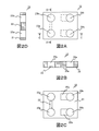
- 2A to 2D are views showing the shape of the chip body of the microchannel chip shown in FIGS. 1A to 1D.
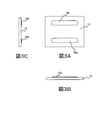
- 3A to 3C are diagrams showing the shape of the film after the carbon ink printing of the microchannel chip shown in FIGS. 1A to 1D.
- FIG. 1B is an enlarged sectional view taken along line EE shown in FIG. 1A.
- 5A to 5C are diagrams showing the shape of the microchannel chip according to the embodiment of the present invention (variation 1).
- 6A to 6C are diagrams showing the shape of the chip body of the microchannel chip shown in FIGS. 5A to 5C.
- FIGS. 1A to 1D are diagrams showing the shape of a microchannel chip as a fluid handling apparatus according to the present embodiment.
- 1A is a plan view
- FIG. 1B is a front sectional view taken along line AA
- FIG. 1C is a bottom view
- FIG. 1D is a left sectional view taken along line BB.
- 1A and 1B show both electrode rods 1a and 1b.
- a microchannel chip 10 includes a transparent substantially rectangular flat plate chip body (substrate member) 12, a film (a thin film serving as a lid member) 14, and carbon ink (as a transmission function unit). Electrode) 16a, 16b.
- the thickness of the chip body 12 is about 1 mm, the thickness of the film 14 is about 100 ⁇ m, and the thickness of the carbon inks 16 a and 16 b is about 10 ⁇ m.
- the chip body 12 and the film 14 are formed of a resin material such as polyethylene terephthalate, polycarbonate, polymethyl methacrylate, vinyl chloride, polypropylene, polyether, polyethylene, and the like. Note that different materials may be used for the chip body 12 and the film 14.
- Carbon inks 16 a and 16 b are printed on the film 14.
- the film 14 is bonded to the chip body 12 by adhesion with an organic adhesive or thermocompression bonding.
- FIGS. 2A to 2D are diagrams showing the shape of the chip body 12.
- 2A is a plan view
- FIG. 2B is a front sectional view taken along the line CC
- FIG. 2C is a bottom view
- FIG. 2D is a left side sectional view taken along the line DD.
- the chip body 12 is provided with elongated fine grooves 22 on a lower surface 21 which is a surface facing the film 14.
- the fine groove 22 has a substantially rectangular cross section having a side length (width and depth) of about several tens of ⁇ m. In the state where the chip body 12 and the film 14 are joined, the opening portion of the fine groove 22 is closed by the film 14, thereby forming the flow path 22 ′.
- through holes 23a and 23b having a substantially circular cross section are formed.
- the diameters of the through holes 23a and 23b are several hundred ⁇ m to several mm.
- the opening portions of the through holes 23a and 23b are closed by the film 14, thereby having a bottomed function having a function as an injection port or a discharge port for the electrophoresis solution or the sample.
- First regions 23a ′ and 23b ′ are formed.
- through holes 24a and 24b having a substantially circular cross section are formed.
- the diameters of the through holes 24a and 24b are several hundred ⁇ m to several mm.
- the opening portions of the through holes 24a and 24b are closed by the film 14, so that the bottomed second having a function as an insertion port for the electrode rods 1a and 1b. Regions 24a 'and 24b' are formed.
- a recess 25a is formed at a position on the carbon ink 16a and connected to the through hole 24a
- a recess 25b is formed at a position on the carbon ink 16b and connected to the through hole 24b.
- the third regions 25a 'and 25b' are filled with conductive adhesives 26a and 26b (see FIGS. 1 and 4).
- the unbonded portion of the chip body 12 and the film 14 generated by the thickness of the carbon inks 16a and 16b becomes an unexpected flow path, and the liquid leaking from the first regions 23a ′ and 23b ′ is the second region 24a ′. , 24b ′ can be prevented.
- 3A to 3C are diagrams showing the shape of the film 14 after the carbon inks 16a and 16b are printed.
- 3A is a plan view
- FIG. 3B is a front view
- FIG. 3C is a left side view.
- the film 14 on which the carbon inks 16a and 16b are printed has a transparent organic adhesive on the lower surface 21 of the chip body 12 so as to cover at least the fine grooves 22, the through holes 23a, 23b, 24a and 24b, and the recesses 25a and 25b. Bonded by bonding or thermocompression bonding.
- both ends of the carbon ink 16a are located in the first region 23a ′ and the second region 24a ′, and both ends of the carbon ink 16b are in the first region 23b ′.
- the carbon inks 16a and 16b are electrically conductive and have a function as an electrode.
- Electrophoresis using microchannel chip First, in the microchannel chip 10, the electrophoresis solution is injected into the first region (injection port) 23a ′ to fill the channel 22 ′. Next, a sample for analysis is injected. Further, the electrode rods 1a and 1b are inserted into the second regions 24a ′ and 24b ′ and brought into contact with the conductive adhesives 26a and 26b.
- the sample is separated by the difference in moving speed for each molecular weight.
- the tester can obtain the result of electrophoresis by detecting the fluorescence intensity.
- FIG. 4 is an enlarged cross-sectional view taken along the line EE of FIG. 1A.
- the peripheral portion of the carbon ink 16b (16a) of the film 14 is not adhered to the chip body 12 (lamination failure), and the carbon ink There is a possibility that gaps 31a and 31b are formed between the chip body 12 and the film 14 at the edge of 16a (16b).
- the gaps 31a and 31b become unexpected flow paths that connect to the first region 23b '(23a'). Therefore, the liquid (electrophoretic solution, sample) injected into the flow path 22 ′ of the micro flow path chip 10 leaks from the first region 23 b ′ (23 a ′) through the gaps 31 a and 31 b due to capillary action.
- the third region 25b '(25a') is formed in the microchannel chip 10 according to the present embodiment.
- the width W1 of the third region 25b '(25a') is formed to be longer than the width W2 of the carbon ink 16b (16a), and the third region 25b '(25a') is connected to the gaps 31a and 31b.
- the opening of the gaps 31a and 31b to the third region 25b '(25a') is closed.
- the liquid does not travel from the first region 23b '(23a') to the second region 24a '(24b') through the gaps 31a and 31b.
- FIGS. 5A to 5C are diagrams showing shapes of variation 1 of the microchannel chip according to the present embodiment.
- the variation 1 microchannel chip 10-1 is used to heat a sample with a heater.
- 5A is a plan view
- FIG. 5B is a front sectional view taken along line FF
- FIG. 5C is a bottom view.
- 5A and 5B show both the electric heater 1a-1.
- 5A to 5C parts common to those in FIGS. 1A to 1D are denoted by the same reference numerals, and detailed description thereof is omitted.
- FIGS. 5A to 5C are diagrams showing the shape of the chip body of the microchannel chip shown in FIGS. 5A to 5C.
- 6A is a plan view
- FIG. 6B is a front sectional view taken along line GG
- FIG. 6C is a bottom view.
- 6A to 6C parts common to those in FIGS. 2A to 2D are denoted by the same reference numerals, and detailed description thereof is omitted.
- Variation 1 is a case where there is only one metal film 16a-1 having a high heat transfer property as the transfer function part. 5A to 5C, the microchannel chip 10-1 is different from the chip body 12 and the film 14 shown in FIGS. 1A to D in the shape of the chip body 12-1 and the film 14-1.
- a through hole 23a, a through hole 24a, and a through hole 27 are formed in the chip body 12-1 one by one. Further, one recess 25a is formed on the lower surface 21-1 of the chip body 12-1. Note that no fine groove is formed in the chip body 12-1.
- the through hole 27 serves as an adhesive inlet 27 ′ that communicates with the third region 25 a ′ in a state where the chip body 12-1 and the film 14-1 are joined.
- the adhesive 26-1 that fills the third region 25a ' is injected from the injection port 27'.
- the adhesive 26-1 is introduced into the third region 25a 'by capillary action, and stops at the opening of the third region 25a' to the second region 24a 'by capillary action. Accordingly, since the metal film 16a-1 in the second region 24a 'is not covered with the adhesive 26-1, the electric heater 1a-1 can be brought into direct contact with the metal film 16a-1.
- the flow of the adhesive 26-1 flowing in the flow path-shaped third region 25a ′ stops when it reaches the opening of the second region 24a ′, which is a large space, and the second region 24a ′.
- the inner transfer function part (metal film) 16a-1 is not covered.
- the adhesive 26-1 only needs to prevent communication between the second region 24a ′ and the third region 25a ′, and is not limited to one having a transmission function. Can do.
- the present invention is not limited to this, and other conductive members and heat transfer members are used. Even if a member is used, the same effect can be obtained.
- the present invention is not limited to this, and a case where a thin plate is joined to the chip body as shown in FIG. A similar effect can be obtained.
- the present invention provides a space between a space (first region) into which a liquid is introduced and a space (second region) electrically or thermally connected to the space (second region).
- a space (third region) communicating with a gap (unexpected flow path) that may occur at the edge of the transmission function portion is formed, and the third region is filled with an adhesive, thereby forming a space in the first region.
- the liquid to be introduced is prevented from leaking into the space of the second region.
- the concave shape of the substrate member for forming the first region and the second region is not limited to the shape shown in the above embodiment.
- the first region may be a space in the middle of the flow path.
- the fluid handling apparatus and fluid handling system according to the present invention can be used in an apparatus that performs high-speed inspection analysis of a very small amount of substances in the scientific field or the medical field such as biochemistry and analytical chemistry.
- Micro-channel chip 12 12-1 Chip body 14, 14-1 Film 16a, 16b Carbon ink 16a-1 Metal film 22 Fine groove 22 'Channel 23a, 23b, 24a, 24b, 27 Through hole 23a', 23b ', 26' First region 24a ', 24b' Second region 25a, 25b Recess 25a ', 25b' Third region 26a ', 26b', 26-1 Adhesive 27 'Inlet
Landscapes
- Chemical & Material Sciences (AREA)
- Chemical Kinetics & Catalysis (AREA)
- Health & Medical Sciences (AREA)
- Clinical Laboratory Science (AREA)
- Analytical Chemistry (AREA)
- Hematology (AREA)
- General Health & Medical Sciences (AREA)
- Dispersion Chemistry (AREA)
- Organic Chemistry (AREA)
- Engineering & Computer Science (AREA)
- Microelectronics & Electronic Packaging (AREA)
- Automatic Analysis And Handling Materials Therefor (AREA)
- Sampling And Sample Adjustment (AREA)
- Physical Or Chemical Processes And Apparatus (AREA)
Abstract
本発明は、ラミネート不良に起因する液体の漏れを防止できるマイクロ流路チップに関する。マイクロ流路チップ(10)のチップ本体(12)の下面(21)にフィルム(14)を接合することにより、有底の第1領域(23a'、23b')、第2領域(24a'、24b')、第3領域(25a'、25b')が形成される。第3領域(25a'、25b')は、第2領域(24a'、24b')に連通し、カーボンインク(16a、16b)上に形成される。第3領域(25a'、25b')の幅は、カーボンインク(16a、16b)の幅より長くなるように形成される。第3領域(25a'、25b')には、導電性の接着剤が充填される。
Description
本発明は、液体試料の分析や処理等に用いられる流体取扱装置及びこれを具備する流体取扱システムに関する。
近年、生化学や分析化学等の科学分野あるいは医学分野において、タンパクや核酸(例えば、DNA)などの微量な物質の検査分析を精度良く高速に行うために、マイクロ分析システムが使用されている。
マイクロ分析システムの一例として、マイクロ流路チップに形成された流路を泳動液(緩衝液)で満たし、流路に繋がる注入口から試料を注入し、流路の両端に電圧をかけ、試料を電気泳動させて分析を行うシステムがある。
マイクロ流路チップは、流路が形成されたチップ本体にフィルム(薄膜)または薄板を接合することにより作製される。流路の両端には、液体が注入されるリザーバが形成され、そのリザーバ内には電極が形成される。電極形成方法の例として、カーボンインクにてフィルムまたは薄板上に電極パターンを印刷する方法が知られている(特許文献1参照)。そのように形成される電極パターンの一端は、リザーバ内に位置するように形成され、他端はリザーバ外に位置するように形成されている。そして、電極パターンの他端に電気泳動装置の電極を接触させ、リザーバ内に注入される液体試料に触れることなく液体試料に電圧がかけられるように構成されている。
上記の電極形成方法では、カーボンインクの厚みにより、フィルムまたは薄板のカーボンインクの周辺部分がチップ本体に未接着となり(ラミネート不良)、液体の漏れが発生するおそれがある。
しかしながら、従来技術では、この液体の漏れについて対策が採られておらず、液体が漏れた場合に、電気泳動装置(電極)が汚染するおそれがある。
本発明の目的は、マイクロ流路チップ等の流体取扱装置から外部への液体の漏れを防止することができ、外部環境の汚染を防止することができる流体取扱装置及び流体取扱システムを提供することである。
本発明の流体取扱装置は、凹みまたは貫通孔が形成された基板部材と、前記基板部材の一方の面に接合された、薄膜状または薄板状の蓋部材と、前記蓋部材の前記基板部材側の面の一部を覆うように層状に形成された、電気または熱を伝達する伝達機能部と、を有し、前記基板部材の前記伝達機能部の一端に対応する部分には、第1領域を形成する凹みまたは貫通孔が形成されており、前記第1領域を形成する凹みまたは貫通孔の前記蓋部材側の開口部は、前記蓋部材により閉塞されており、前記基板部材の前記伝達機能部の他端に対応する部分には、外部に連通する第2領域が形成されており、前記伝達機能部は、前記第1領域と前記第2領域との間を電気的または熱的に接続しており、前記基板部材の前記伝達機能部の前記一端および前記他端との間の部分に対応する部分には、第3領域を形成する凹みが前記伝達機能部の縁部に架かるように形成されており、前記第3領域を形成する凹みの前記蓋部材側の開口部は、前記蓋部材により閉塞されており、前記第3領域は、前記第2領域と連通しており、かつ接着剤で充填されている、構成を採る。
本発明の流体取扱装置システムは、上記流体取扱装置を備える構成を採る。
本発明によれば、基板部材に凹みを形成し、この凹みが薄膜または薄板によって閉塞されてできる空間(第3領域)を接着剤で充填することにより、層状の伝達機能部の厚みによって生じる基板部材と蓋部材との隙間を伝わって漏れてきた液体の漏れを防止することができ、外部環境の汚染を防止することができる。
以下、本発明の実施の形態について、図面を参照して詳細に説明する。
〔マイクロ流路チップの構成〕
図1A~Dは、本実施の形態に係る流体取扱装置としてのマイクロ流路チップの形状を示す図である。図1Aは平面図、図1BはA-A線正面断面図、図1Cは底面図、図1DはB-B線左側面断面図である。なお、図1Aおよび図1Bには、電極棒1a、1bをともに示す。
図1A~Dは、本実施の形態に係る流体取扱装置としてのマイクロ流路チップの形状を示す図である。図1Aは平面図、図1BはA-A線正面断面図、図1Cは底面図、図1DはB-B線左側面断面図である。なお、図1Aおよび図1Bには、電極棒1a、1bをともに示す。
図1A~Dに示すように、マイクロ流路チップ10は、透明な略矩形の平板のチップ本体(基板部材)12とフィルム(蓋部材となる薄膜)14と、カーボンインク(伝達機能部としての電極)16a、16bと、から構成される。
チップ本体12の厚さは1mm程度であり、フィルム14の厚さは100μm程度であり、カーボンインク16a、16bの厚さは10μm程度である。
チップ本体12およびフィルム14は、例えばポリエチレンテレフタレート、ポリカーボネート、ポリメタクリル酸メチル、塩化ビニール、ポリプロピレン、ポリエーテル、ポリエチレンなどの樹脂材料によって形成されている。なお、チップ本体12とフィルム14とで、互いに異なる材料を用いても良い。
カーボンインク16a、16bは、フィルム14に印刷される。フィルム14は、有機接着剤による接着あるいは熱圧着等によりチップ本体12に接合される。
図2A~Dは、チップ本体12の形状を示す図である。図2Aは平面図、図2BはC-C線正面断面図、図2Cは底面図、図2DはD-D線左側面断面図である。
チップ本体12には、フィルム14に対向する面である下面21に、細長い微細溝22が形成される。微細溝22は、一辺の長さ(幅および深さ)が数十μm程度の略矩形の断面を有する。チップ本体12とフィルム14とが接合された状態において、微細溝22の開口部分がフィルム14によって閉塞されることにより流路22’が形成される。
チップ本体12の微細溝22のそれぞれの両端には、外部に開口する、断面が略円形の貫通孔23a、23bが形成される。貫通孔23a、23bの直径は、数100μm~数mmである。チップ本体12とフィルム14とが接合された状態において、貫通孔23a、23bの開口部分がフィルム14によって閉塞されることにより、泳動液、試料の注入口又は排出口としての機能を有する有底の第1領域23a’、23b’が形成される。
チップ本体12には、断面が略円形の貫通孔24a、24bが形成される。貫通孔24a、24bの直径は、数100μm~数mmである。チップ本体12とフィルム14とが接合された状態において、貫通孔24a、24bの開口部分がフィルム14によって閉塞されることにより、電極棒1a、1bの挿入口としての機能を有する有底の第2領域24a’、24b’が形成される。
チップ本体12の下面21には、カーボンインク16a上の位置に貫通孔24aに連接して凹み25aが形成され、カーボンインク16b上の位置に貫通孔24bに連接して凹み25bが形成される。そして、チップ本体12とフィルム14とが接合された状態において、凹み25a、25bの開口部がフィルム14によって閉塞されることにより第3領域25a’、25b’が形成される。第3領域25a’、25b’は、カーボンインク16a、16b上に位置する。第3領域25a’、25b’の幅は、カーボンインク16a、16bの幅より長くなるように形成される(図4参照)。第3領域25a’、25b’には、導電性の接着剤26a、26b(図1、図4参照)が充填される。これにより、カーボンインク16a、16bの厚みによって生じるチップ本体12とフィルム14の未接着部分が予期しない流路となって、第1領域23a’、23b’から漏れてきた液体が第2領域24a’、24b’に到達することを防止することができる。
図3A~Cは、カーボンインク16a、16b印刷後のフィルム14の形状を示す図である。図3Aは平面図、図3Bは正面図、図3Cは左側面図である。
カーボンインク16a、16bが印刷されたフィルム14は、少なくとも微細溝22、貫通孔23a、23b、24a、24b、凹み25a、25bを覆うように、チップ本体12の下面21に、透明な有機接着剤による接着あるいは熱圧着等により接合される。
フィルム14をチップ本体12に接合した際には、カーボンインク16aの両端が第1領域23a’の中および第2領域24a’の中に位置し、カーボンインク16bの両端が第1領域23b’の中および第2領域24b’の中に位置する。カーボンインク16a、16bは、導電性があり、電極としての機能を有する。
〔マイクロ流路チップによる電気泳動〕
まず、マイクロ流路チップ10において、第1領域(注入口)23a’に泳動液を注入し、流路22’を充填する。次に分析用の試料を注入する。また、電極棒1a、1bを、第2領域24a’、24b’に挿入して導電性接着剤26a、26bに接触させる。
まず、マイクロ流路チップ10において、第1領域(注入口)23a’に泳動液を注入し、流路22’を充填する。次に分析用の試料を注入する。また、電極棒1a、1bを、第2領域24a’、24b’に挿入して導電性接着剤26a、26bに接触させる。
そして、電極棒1a、1bに通電することにより、流路22’の両端に電圧をかける。これにより、試料は、第1領域(排出口)23b’に向かって流路22’内を移動する。
流路22’内において、試料は、分子量毎の移動速度の違いによって分離される。試験者は、蛍光強度を検出することにより、電気泳動の結果を得ることができる。
〔本実施の形態の効果〕
図4は、図1AのE-E線拡大断面図である。図4に示すように、カーボンインクの16b(16a)の厚みに起因して、フィルム14のカーボンインクの16b(16a)の周辺部分がチップ本体12に未接着となり(ラミネート不良)、カーボンインクの16a(16b)の縁部において、チップ本体12とフィルム14との間に隙間31a、31bが生じる虞がある。
図4は、図1AのE-E線拡大断面図である。図4に示すように、カーボンインクの16b(16a)の厚みに起因して、フィルム14のカーボンインクの16b(16a)の周辺部分がチップ本体12に未接着となり(ラミネート不良)、カーボンインクの16a(16b)の縁部において、チップ本体12とフィルム14との間に隙間31a、31bが生じる虞がある。
隙間31a、31bは、第1領域23b’(23a’)に繋がる予期しない流路となる。したがって、マイクロ流路チップ10の流路22’に注入した液体(泳動液、試料)が、毛細管現象により、第1領域23b’(23a’)から隙間31a、31bを伝わって漏れてくる。
本実施の形態に係るマイクロ流路チップ10には、第3領域25b’(25a’)が形成される。第3領域25b’(25a’)の幅W1は、カーボンインク16b(16a)の幅W2より長くなるように形成され、第3領域25b’(25a’)は隙間31a、31bと繋がっている。この第3領域25b’(25a’)に導電性の接着剤26b(26a)を充填することにより、隙間31a、31bの第3領域25b’(25a’)への開口部が塞がる。
したがって、第1領域23b’(23a’)から、液体が、隙間31a、31bを伝わって第2領域24a’(24b’)に行くことはない。
この結果、本実施の形態によれば、液体の外部への漏れを防止することができ、電極や外部環境の汚染を防止することができる。
[バリエーション]
以下、本実施の形態に係るマイクロ流路チップのバリエーションについて説明する。
以下、本実施の形態に係るマイクロ流路チップのバリエーションについて説明する。
[バリエーション1]
図5A~Cは、本実施の形態に係るマイクロ流路チップのバリエーション1の形状を示す図である。バリエーション1のマイクロ流路チップ10-1は、試料をヒータで加熱するために用いられる。図5Aは平面図、図5BはF-F線正面断面図、図5Cは底面図である。なお、図5Aおよび図5Bには、電熱ヒータ1a-1をともに示す。なお、図5A~Cにおいて、図1A~Dと共通する部分には、同一の符号を付して詳しい説明を省略する。
図5A~Cは、本実施の形態に係るマイクロ流路チップのバリエーション1の形状を示す図である。バリエーション1のマイクロ流路チップ10-1は、試料をヒータで加熱するために用いられる。図5Aは平面図、図5BはF-F線正面断面図、図5Cは底面図である。なお、図5Aおよび図5Bには、電熱ヒータ1a-1をともに示す。なお、図5A~Cにおいて、図1A~Dと共通する部分には、同一の符号を付して詳しい説明を省略する。
図6A~Cは、図5A~Cに示されるマイクロ流路チップのチップ本体の形状を示す図である。図6Aは平面図、図6BはG-G線正面断面図、図6Cは底面図である。なお、図6A~Cにおいて、図2A~Dと共通する部分には、同一の符号を付して詳しい説明を省略する。
バリエーション1は、伝達機能部としての伝熱性に富む金属膜16a-1が一つのみの場合である。図5A~Cにおいて、マイクロ流路チップ10-1は、チップ本体12-1、フィルム14-1の形状が図1A~Dに示されるチップ本体12、フィルム14と異なる。
また、図6A~Cにおいて、チップ本体12-1には、貫通孔23a、貫通孔24a、貫通孔27が一つずつ形成される。また、チップ本体12-1の下面21-1には、凹み25aが一つ形成される。なお、チップ本体12-1には、微細溝は形成されていない。
貫通孔27は、チップ本体12-1とフィルム14-1とが接合された状態において、第3領域25a’と連通する接着剤の注入口27’となる。バリエーション1のマイクロ流路チップ10-1は、第3領域25a’を充填させる接着剤26-1を注入口27’より注入する。接着材26-1は毛細管現象によって第3領域25a’へ導入され、毛細管現象によって第3領域25a’の第2領域24a’への開口部で止まる。これより、第2領域24a’内の金属膜16a-1は接着剤26-1で覆われないため、電熱ヒータ1a-1を金属膜16a-1に直接、接触させることができる。
このように、流路状の第3領域25a’内を流動する接着剤26-1は、広い空間である第2領域24a’の開口部に達したところでその流れは止まり、第2領域24a’内の伝達機能部(金属膜)16a-1を覆い隠すことはない。接着剤26-1は、第2領域24a’と第3領域25a’との間が連通するのを妨げるものであればよく、伝達機能を有するものに限定されないため、選択の自由度を広げることができる。
バリエーション1によっても、第1領域23a’から漏れてきた液体が、第3領域25a’に止められ、第2領域24a’に到達するのを防ぐことができる。この結果、液体の漏れを防止することができ、外部環境の汚染を防止することができ、電熱ヒータ1a-1によって安全に第1領域23a’内に注入された試料を加熱することができる。
なお、上記実施の形態としては、導電部材としてカーボンインク16a、16b、伝熱部材として金属膜16a-1を用いる場合について説明したが、本発明はこれに限られず、他の導電部材や伝熱部材を用いても同様の効果を得ることができる。
また、上記実施の形態としては、フィルム14をチップ本体12に接合する場合について説明したが、本発明はこれに限られず、特許文献1の図1のように、薄板をチップ本体に接合する場合にも同様の効果を得ることができる。
本発明は、上記実施の形態に示す通り、液体が導入される空間(第1領域)と、これに電気的または熱的に伝達機能部によって接続されている空間(第2領域)との間に、伝達機能部の縁部に生じ得る隙間(予期しない流路)に連通する空間(第3領域)を形成し、この第3領域を接着剤で充填させることによって、第1領域の空間に導入される液体が第2領域の空間に漏れ出るのを防ぐものである。この効果が得られるものであれば、第1領域および第2領域を形成するための基板部材の凹み形状は上記実施の形態において示した形状に限られない。第1領域は、流路の途中の空間であってもよい。
本出願は、2011年4月4日出願の特願2011-082820に基づく優先権を主張する。当該出願明細書および図面に記載された内容は、すべて本願明細書に援用される。
本発明に係る流体取扱装置及び流体取扱システムは、生化学や分析化学等の科学分野あるいは医学分野において、微量な物質の検査分析を精度良く高速に行う装置に使用することができる。
10 マイクロ流路チップ
12、12-1 チップ本体
14、14-1 フィルム
16a、16b カーボンインク
16a-1 金属膜
22 微細溝
22’ 流路
23a、23b、24a、24b、27 貫通孔
23a’、23b’、26’ 第1領域
24a’、24b’ 第2領域
25a、25b 凹み
25a’、25b’ 第3領域
26a’、26b’、26-1 接着剤
27’ 注入口
12、12-1 チップ本体
14、14-1 フィルム
16a、16b カーボンインク
16a-1 金属膜
22 微細溝
22’ 流路
23a、23b、24a、24b、27 貫通孔
23a’、23b’、26’ 第1領域
24a’、24b’ 第2領域
25a、25b 凹み
25a’、25b’ 第3領域
26a’、26b’、26-1 接着剤
27’ 注入口
Claims (3)
- 凹みまたは貫通孔が形成された基板部材と、
前記基板部材の一方の面に接合された、薄膜状または薄板状の蓋部材と、
前記蓋部材の前記基板部材側の面の一部を覆うように層状に形成された、電気または熱を伝達する伝達機能部と、を有し、
前記基板部材の前記伝達機能部の一端に対応する部分には、第1領域を形成する凹みまたは貫通孔が形成されており、
前記第1領域を形成する凹みまたは貫通孔の前記蓋部材側の開口部は、前記蓋部材により閉塞されており、
前記基板部材の前記伝達機能部の他端に対応する部分には、外部に連通する第2領域が形成されており、
前記伝達機能部は、前記第1領域と前記第2領域との間を電気的または熱的に接続しており、
前記基板部材の前記伝達機能部の前記一端および前記他端との間の部分に対応する部分には、第3領域を形成する凹みが前記伝達機能部の縁部に架かるように形成されており、
前記第3領域を形成する凹みの前記蓋部材側の開口部は、前記蓋部材により閉塞されており、
前記第3領域は、前記第2領域と連通しており、かつ接着剤で充填されている、
流体取扱装置。 - 前記接着剤が、導電性または伝熱性を有する、請求項1に記載の流体取扱装置。
- 請求項1に記載の流体取扱装置を具備する流体取扱システム。
Priority Applications (1)
| Application Number | Priority Date | Filing Date | Title |
|---|---|---|---|
| US14/110,086 US9120098B2 (en) | 2011-04-04 | 2012-03-12 | Fluid handling device and fluid handling system |
Applications Claiming Priority (2)
| Application Number | Priority Date | Filing Date | Title |
|---|---|---|---|
| JP2011082820A JP5723198B2 (ja) | 2011-04-04 | 2011-04-04 | 流体取扱装置及び流体取扱システム |
| JP2011-082820 | 2011-04-04 |
Publications (1)
| Publication Number | Publication Date |
|---|---|
| WO2012137413A1 true WO2012137413A1 (ja) | 2012-10-11 |
Family
ID=46968829
Family Applications (1)
| Application Number | Title | Priority Date | Filing Date |
|---|---|---|---|
| PCT/JP2012/001690 Ceased WO2012137413A1 (ja) | 2011-04-04 | 2012-03-12 | 流体取扱装置及び流体取扱システム |
Country Status (3)
| Country | Link |
|---|---|
| US (1) | US9120098B2 (ja) |
| JP (1) | JP5723198B2 (ja) |
| WO (1) | WO2012137413A1 (ja) |
Families Citing this family (2)
| Publication number | Priority date | Publication date | Assignee | Title |
|---|---|---|---|---|
| GB2515571A (en) * | 2013-06-28 | 2014-12-31 | Ibm | Fabrication of microfluidic chips having electrodes level with microchannel walls |
| CN113634296B (zh) * | 2021-10-19 | 2022-02-11 | 北京芯迈微生物技术有限公司 | 一种微流控芯片 |
Citations (2)
| Publication number | Priority date | Publication date | Assignee | Title |
|---|---|---|---|---|
| JP2006142198A (ja) * | 2004-11-19 | 2006-06-08 | Starlite Co Ltd | マイクロ化学デバイス及びその製造方法 |
| JP2006517652A (ja) * | 2002-12-26 | 2006-07-27 | メソ スケイル テクノロジーズ,エルエルシー | アッセイカートリッジ及び同アッセイカートリッジを用いた方法 |
Family Cites Families (11)
| Publication number | Priority date | Publication date | Assignee | Title |
|---|---|---|---|---|
| JP4178653B2 (ja) * | 1999-02-26 | 2008-11-12 | 日立化成工業株式会社 | 電気泳動用チップとその製造方法、該電気泳動用チップを用いた電気泳動装置及び荷電性物質の分離方法 |
| US6939451B2 (en) | 2000-09-19 | 2005-09-06 | Aclara Biosciences, Inc. | Microfluidic chip having integrated electrodes |
| US6692700B2 (en) * | 2001-02-14 | 2004-02-17 | Handylab, Inc. | Heat-reduction methods and systems related to microfluidic devices |
| US20040241381A1 (en) * | 2002-01-31 | 2004-12-02 | Chen Yihfar | Microfluidic structures with circumferential grooves for bonding adhesives and related optical analysis discs |
| US20070286773A1 (en) * | 2002-05-16 | 2007-12-13 | Micronit Microfluidics B.V. | Microfluidic Device |
| JP3880930B2 (ja) * | 2002-07-26 | 2007-02-14 | 株式会社エンプラス | プレートの接着部構造 |
| JP2005055320A (ja) * | 2003-08-05 | 2005-03-03 | Pentax Corp | 電気泳動チップ |
| JP4591054B2 (ja) * | 2004-11-24 | 2010-12-01 | パナソニック株式会社 | 光学的分析デバイス |
| US20070102293A1 (en) * | 2005-09-07 | 2007-05-10 | Yu-Chong Tai | Electrochemical flow cell, an assembly of and a method of fabrication of the same |
| JP4942094B2 (ja) * | 2007-01-12 | 2012-05-30 | 独立行政法人産業技術総合研究所 | 電極付きガラス製マイクロチップ基板の製造方法 |
| WO2011026136A1 (en) * | 2009-08-31 | 2011-03-03 | Life Technologies Corporation | Low-volume sequencing system and method of use |
-
2011
- 2011-04-04 JP JP2011082820A patent/JP5723198B2/ja not_active Expired - Fee Related
-
2012
- 2012-03-12 WO PCT/JP2012/001690 patent/WO2012137413A1/ja not_active Ceased
- 2012-03-12 US US14/110,086 patent/US9120098B2/en not_active Expired - Fee Related
Patent Citations (2)
| Publication number | Priority date | Publication date | Assignee | Title |
|---|---|---|---|---|
| JP2006517652A (ja) * | 2002-12-26 | 2006-07-27 | メソ スケイル テクノロジーズ,エルエルシー | アッセイカートリッジ及び同アッセイカートリッジを用いた方法 |
| JP2006142198A (ja) * | 2004-11-19 | 2006-06-08 | Starlite Co Ltd | マイクロ化学デバイス及びその製造方法 |
Also Published As
| Publication number | Publication date |
|---|---|
| US9120098B2 (en) | 2015-09-01 |
| JP2012220205A (ja) | 2012-11-12 |
| JP5723198B2 (ja) | 2015-05-27 |
| US20140023566A1 (en) | 2014-01-23 |
Similar Documents
| Publication | Publication Date | Title |
|---|---|---|
| JP5797926B2 (ja) | 流体取扱装置およびその製造方法ならびに流体取扱システム | |
| US8920727B2 (en) | Arrangement and method for electrochemically measuring biochemical reactions and method for producing the arrangement | |
| JP4362987B2 (ja) | マイクロチップ電気泳動におけるサンプル導入方法 | |
| JP4831232B2 (ja) | 電気泳動装置及び電気泳動方法 | |
| US9101932B2 (en) | Fluid handling apparatus | |
| CN101588868B (zh) | 具有用于流体引入的侧面开口的微流体芯片 | |
| JP5723198B2 (ja) | 流体取扱装置及び流体取扱システム | |
| JP3880930B2 (ja) | プレートの接着部構造 | |
| US9387477B2 (en) | Fluid handling device | |
| US9234791B2 (en) | Light emission detection device having a flow path formed by a depression of a detection side substrate and method of manufacturing the same | |
| JP5723197B2 (ja) | 流体取扱装置及び流体取扱システム | |
| US8277761B2 (en) | Channelless fluidic sample transport medium | |
| CN117019242A (zh) | 一种集成温度传感器的微流控芯片封装结构及封装方法 | |
| US9283558B2 (en) | Fluid handling device | |
| US20190270255A1 (en) | Ultrasonic welding of a microfluidic device | |
| Bressan et al. | Microchip electrophoresis containing electrodes for integrated electrochemical detection | |
| WO2024088766A1 (en) | Lab-on-pcb device and method for manufacturing thereof | |
| WO2021053196A1 (en) | Conductive spacer for a microfluidic device |
Legal Events
| Date | Code | Title | Description |
|---|---|---|---|
| 121 | Ep: the epo has been informed by wipo that ep was designated in this application |
Ref document number: 12768120 Country of ref document: EP Kind code of ref document: A1 |
|
| NENP | Non-entry into the national phase |
Ref country code: DE |
|
| WWE | Wipo information: entry into national phase |
Ref document number: 14110086 Country of ref document: US |
|
| 122 | Ep: pct application non-entry in european phase |
Ref document number: 12768120 Country of ref document: EP Kind code of ref document: A1 |