WO2012133890A1 - Display panel unevenness correction method, correction system - Google Patents
Display panel unevenness correction method, correction system Download PDFInfo
- Publication number
- WO2012133890A1 WO2012133890A1 PCT/JP2012/058908 JP2012058908W WO2012133890A1 WO 2012133890 A1 WO2012133890 A1 WO 2012133890A1 JP 2012058908 W JP2012058908 W JP 2012058908W WO 2012133890 A1 WO2012133890 A1 WO 2012133890A1
- Authority
- WO
- WIPO (PCT)
- Prior art keywords
- correction
- correction data
- display panel
- unit
- data
- Prior art date
Links
Images


Classifications
-
- G—PHYSICS
- G09—EDUCATION; CRYPTOGRAPHY; DISPLAY; ADVERTISING; SEALS
- G09G—ARRANGEMENTS OR CIRCUITS FOR CONTROL OF INDICATING DEVICES USING STATIC MEANS TO PRESENT VARIABLE INFORMATION
- G09G5/00—Control arrangements or circuits for visual indicators common to cathode-ray tube indicators and other visual indicators
- G09G5/02—Control arrangements or circuits for visual indicators common to cathode-ray tube indicators and other visual indicators characterised by the way in which colour is displayed
-
- G—PHYSICS
- G09—EDUCATION; CRYPTOGRAPHY; DISPLAY; ADVERTISING; SEALS
- G09G—ARRANGEMENTS OR CIRCUITS FOR CONTROL OF INDICATING DEVICES USING STATIC MEANS TO PRESENT VARIABLE INFORMATION
- G09G3/00—Control arrangements or circuits, of interest only in connection with visual indicators other than cathode-ray tubes
- G09G3/006—Electronic inspection or testing of displays and display drivers, e.g. of LED or LCD displays
-
- G—PHYSICS
- G02—OPTICS
- G02F—OPTICAL DEVICES OR ARRANGEMENTS FOR THE CONTROL OF LIGHT BY MODIFICATION OF THE OPTICAL PROPERTIES OF THE MEDIA OF THE ELEMENTS INVOLVED THEREIN; NON-LINEAR OPTICS; FREQUENCY-CHANGING OF LIGHT; OPTICAL LOGIC ELEMENTS; OPTICAL ANALOGUE/DIGITAL CONVERTERS
- G02F1/00—Devices or arrangements for the control of the intensity, colour, phase, polarisation or direction of light arriving from an independent light source, e.g. switching, gating or modulating; Non-linear optics
- G02F1/01—Devices or arrangements for the control of the intensity, colour, phase, polarisation or direction of light arriving from an independent light source, e.g. switching, gating or modulating; Non-linear optics for the control of the intensity, phase, polarisation or colour
- G02F1/13—Devices or arrangements for the control of the intensity, colour, phase, polarisation or direction of light arriving from an independent light source, e.g. switching, gating or modulating; Non-linear optics for the control of the intensity, phase, polarisation or colour based on liquid crystals, e.g. single liquid crystal display cells
- G02F1/1306—Details
- G02F1/1309—Repairing; Testing
-
- G—PHYSICS
- G02—OPTICS
- G02F—OPTICAL DEVICES OR ARRANGEMENTS FOR THE CONTROL OF LIGHT BY MODIFICATION OF THE OPTICAL PROPERTIES OF THE MEDIA OF THE ELEMENTS INVOLVED THEREIN; NON-LINEAR OPTICS; FREQUENCY-CHANGING OF LIGHT; OPTICAL LOGIC ELEMENTS; OPTICAL ANALOGUE/DIGITAL CONVERTERS
- G02F2201/00—Constructional arrangements not provided for in groups G02F1/00 - G02F7/00
- G02F2201/58—Arrangements comprising a monitoring photodetector
-
- G—PHYSICS
- G09—EDUCATION; CRYPTOGRAPHY; DISPLAY; ADVERTISING; SEALS
- G09G—ARRANGEMENTS OR CIRCUITS FOR CONTROL OF INDICATING DEVICES USING STATIC MEANS TO PRESENT VARIABLE INFORMATION
- G09G2320/00—Control of display operating conditions
- G09G2320/02—Improving the quality of display appearance
- G09G2320/0233—Improving the luminance or brightness uniformity across the screen
-
- G—PHYSICS
- G09—EDUCATION; CRYPTOGRAPHY; DISPLAY; ADVERTISING; SEALS
- G09G—ARRANGEMENTS OR CIRCUITS FOR CONTROL OF INDICATING DEVICES USING STATIC MEANS TO PRESENT VARIABLE INFORMATION
- G09G2320/00—Control of display operating conditions
- G09G2320/02—Improving the quality of display appearance
- G09G2320/0285—Improving the quality of display appearance using tables for spatial correction of display data
-
- G—PHYSICS
- G09—EDUCATION; CRYPTOGRAPHY; DISPLAY; ADVERTISING; SEALS
- G09G—ARRANGEMENTS OR CIRCUITS FOR CONTROL OF INDICATING DEVICES USING STATIC MEANS TO PRESENT VARIABLE INFORMATION
- G09G2320/00—Control of display operating conditions
- G09G2320/06—Adjustment of display parameters
- G09G2320/0693—Calibration of display systems
-
- G—PHYSICS
- G09—EDUCATION; CRYPTOGRAPHY; DISPLAY; ADVERTISING; SEALS
- G09G—ARRANGEMENTS OR CIRCUITS FOR CONTROL OF INDICATING DEVICES USING STATIC MEANS TO PRESENT VARIABLE INFORMATION
- G09G2360/00—Aspects of the architecture of display systems
- G09G2360/14—Detecting light within display terminals, e.g. using a single or a plurality of photosensors
- G09G2360/145—Detecting light within display terminals, e.g. using a single or a plurality of photosensors the light originating from the display screen
-
- G—PHYSICS
- G09—EDUCATION; CRYPTOGRAPHY; DISPLAY; ADVERTISING; SEALS
- G09G—ARRANGEMENTS OR CIRCUITS FOR CONTROL OF INDICATING DEVICES USING STATIC MEANS TO PRESENT VARIABLE INFORMATION
- G09G3/00—Control arrangements or circuits, of interest only in connection with visual indicators other than cathode-ray tubes
- G09G3/20—Control arrangements or circuits, of interest only in connection with visual indicators other than cathode-ray tubes for presentation of an assembly of a number of characters, e.g. a page, by composing the assembly by combination of individual elements arranged in a matrix no fixed position being assigned to or needed to be assigned to the individual characters or partial characters
- G09G3/34—Control arrangements or circuits, of interest only in connection with visual indicators other than cathode-ray tubes for presentation of an assembly of a number of characters, e.g. a page, by composing the assembly by combination of individual elements arranged in a matrix no fixed position being assigned to or needed to be assigned to the individual characters or partial characters by control of light from an independent source
- G09G3/36—Control arrangements or circuits, of interest only in connection with visual indicators other than cathode-ray tubes for presentation of an assembly of a number of characters, e.g. a page, by composing the assembly by combination of individual elements arranged in a matrix no fixed position being assigned to or needed to be assigned to the individual characters or partial characters by control of light from an independent source using liquid crystals
- G09G3/3611—Control of matrices with row and column drivers
- G09G3/3648—Control of matrices with row and column drivers using an active matrix
Definitions
- the present invention relates to a display panel unevenness correction method and correction system, and more particularly, to a technique for correcting display panel unevenness.
- luminance unevenness and color unevenness that occurs in a display image
- display unevenness greatly affect image quality. It is necessary to correct appropriately.
- Patent Document 1 a technique for correcting display unevenness has been disclosed (for example, Patent Document 1).
- the correction device of the prior art an image displayed on the display panel is shot using a shooting device, correction data is generated based on the shooting result, and the correction data is written in the nonvolatile storage device.
- the correction data is read from the nonvolatile storage device of the correction device, and the image data is corrected using the correction data.
- the present invention has been made in view of such a situation, and an object thereof is to reduce the time required for correcting the unevenness of the display panel.
- the present invention is a display panel unevenness correction method for correcting display unevenness of a display panel, and includes a supplying step of supplying image data to the display panel to display the display panel; A photographing step of photographing the displayed display area of the display panel; a generating step of generating correction data of the display panel from a photographing result of the photographing step; and a storage step of storing the correction data in a volatile storage device; A correction step of correcting the image data using the correction data stored in the volatile storage device to generate corrected image data; supplying the corrected image data to the display panel; A re-feeding step for displaying, and a repeating step for repeatedly executing the steps from the photographing step to the re-feeding step.
- this display panel unevenness correction method the steps from the photographing step to the resupply step are repeatedly executed, and the correction data obtained thereby is stored in the volatile storage device.
- this display panel driving method by using a volatile storage device as a storage device for storing the correction data, the time for writing the correction data in the storage device and the correction data are compared with the case of using the nonvolatile storage device.
- Various times such as the time to erase the data from the storage device can be shortened, and even if the correction data is erased and written multiple times by repeating the steps from the photographing process to the resupply process, the display panel The time required for unevenness correction can be shortened.
- first correction data generated from the imaging result of the imaging step included in the repetition step and second correction data that is correction data generated in the previous generation step
- the correction data is generated by adding together. Accordingly, it is possible to generate correction data with higher accuracy by combining correction data generated in a plurality of correction steps, and display unevenness can be corrected with high accuracy.
- the image data is image data having the same luminance and chromaticity information in the entire display area of the display panel, and the generation circuit is configured so that a variation in the photographing result is within a predetermined specified range. It is preferable to generate the first correction data. As a result, for example, the first correction data is generated so that the variation in the photographing result when the gradation solid pattern is displayed is within a specified range determined based on human vision or the like, thereby accurately displaying unevenness. It can be corrected well.
- the determination step is executed prior to executing the repetition step again after the execution of the repetition step.
- This unevenness correction method for a display panel includes a determining step for determining whether or not to execute a repeating step. Therefore, when sufficient correction image data can be generated in one repeating process, that is, display unevenness can be corrected with high accuracy using the corrected image data generated through one repeating process. In this case, it is possible to reduce the time required for correcting the unevenness of the display panel by suppressing the second and third repeated steps.
- the determining step includes the photographing step, and when the variation in the photographing result in the photographing step is within the specified range, it is determined that the repeating step is not performed, and the variation is larger than the predetermined range.
- the imaging process included in the determination process also serves as the imaging process of the repetition process.
- this unevenness correction method for a display panel when it is determined that the variation in the photographing result is larger than the specified range in the determination step, and the repetition step is executed after the determination step, the same in the determination step and the repetition step. Thus, it is possible to reduce the time required for correcting the unevenness of the display panel.
- the supply step is preferably performed using a liquid crystal panel using liquid crystal. Thereby, display unevenness of a liquid crystal panel used for a large screen television or the like can be suppressed with high accuracy.
- the present invention is also embodied in a correction system that realizes the above-described unevenness correction method.
- the present invention is a correction system that corrects display unevenness of a display panel, a supply unit that supplies image data to the display panel and displays the display panel, a photographing unit that captures a display area of the display panel, Using the correction data stored in the storage unit, a generation unit that generates correction data of the display panel from the imaging result of the imaging device, the volatile storage unit that stores the correction data, and the image data A correction unit that generates corrected image data that has been corrected, and the correction image data supplied to the display panel to generate correction data again from the shooting result that was shot when the display panel was displayed. And a control unit that controls each of the units so as to generate corrected image data again from the correction data.
- the generation unit generates correction data, and the corrected image data generated from the correction data generated by the generation unit again using the correction data is displayed on the display panel. That is, the corrected image data finally generated is corrected a plurality of times by the correction unit.
- this correction system by using a volatile storage unit as the storage unit, various times can be shortened compared to the case of using a non-volatile storage unit, and the correction unit has performed correction multiple times. Even in this case, the time required for correcting the unevenness of the display panel can be shortened.
- the generation unit inputs the generated correction data to the correction unit, and inputs the same correction data multiple times when the correction data is input to the correction unit.
- the unit preferably checks whether or not the correction data input at different timings match.
- the correction unit to which correction data is input checks whether the correction data input at different timings match. That is, a so-called Verify operation is performed to check for a write mismatch associated with a communication error.
- Verify operation is performed to check for a write mismatch associated with a communication error.
- this correction system it is possible to detect a communication error for data that is only input from the outside and is not output to the outside, such as correction data for the correction unit. Accordingly, generation of corrected image data using the correction data in which a communication error has occurred is suppressed, and display unevenness of the display panel can be corrected with high accuracy.
- an input line through which the image data is input to the correction unit and an input line through which the correction data is input to the correction unit are the same.
- communication errors can be detected even when correction data is sent using an input line to which data whose transmission direction is determined in advance, such as image data, is input, and display unevenness of the display panel can be accurately detected. It can be corrected well.
- the correction unit is configured to be connectable to an output line that outputs an inspection result obtained by inspecting the correction data.
- the inspection result obtained by inspecting the correction data inspection result by the correction unit using the output line can be read out of the correction unit, and the inspection result can be reflected in the processing of the correction system.
- the output line is equal to a supply line that supplies the corrected image data to the display panel, and the correction unit has an identification symbol indicating the inspection result, and the identification symbol is set according to the inspection result.
- This display device outputs an inspection result of correction data to the outside of the correction unit by displaying an identification symbol on the display panel.
- the generation unit confirms the captured image input via the imaging unit and detects that the captured image includes an identification symbol indicating that the correction data does not match, the generation unit again corrects the correction data to the correction unit. Enter. Thereby, it is possible to suppress generation of corrected image data based on correction data input when a communication error occurs.
- the generation unit has a plurality of conversion patterns for converting the correction data, and when the same correction data is input to the correction unit a plurality of times, conversion is performed using at least two conversion patterns. It is preferable to input the corrected data to the correction unit.
- a non-volatile second storage unit that stores the correction data may be further provided.
- the control unit generates the second correction data and the second corrected image data, and then controls the display unit and the photographing unit to display the second corrected image data on the display panel.
- the generation unit and the correction unit are controlled to generate new corrected image data from the shooting result.
- the generation unit and the correction unit are controlled to input the second correction data from the generation unit to the correction unit, and from the correction unit
- the generation unit stores the second correction data in the correction unit a plurality of times when the variation in the photographing result is within the specified range. Masui.
- this correction system when correction data in which the variation in the photographing result is within the specified range is generated, the verification work is executed on the correction data. According to this correction system, it is possible to suppress occurrence of a communication error in the correction data in which the variation in the photographing result is within the specified range, and it is possible to accurately correct the display unevenness of the display panel.
- amendment system 1 The figure which shows schematic structure of the liquid crystal display device 10.
- Flow chart showing processing of correction system 1 Flow chart showing initial correction processing
- Flow chart showing saving process 6 is a flowchart illustrating a reading process according to the first embodiment.
- the figure which shows the required time of this embodiment Diagram showing the time required for the prior art 7 is a flowchart illustrating reading processing according to the second embodiment.
- ⁇ Embodiment 1> The first embodiment will be described with reference to the drawings. In the following embodiments, description will be made using a liquid crystal display device including a liquid crystal panel as the display device.
- the display device to which the present invention can be applied is not limited to this, and can also be applied to an active matrix display device such as a PDP (plasma display panel) display device or an organic EL (electroluminescence) display device. is there.
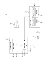
- the system 1 includes a liquid crystal display device 10, a signal source 62, a computer 64, and a camera (an example of a photographing unit) 66.
- the liquid crystal display device 10 includes a supply circuit 12 and a liquid crystal panel (an example of a display panel) 40, and is connected to a signal source 62 via an input line 18.
- the supply circuit 12 supplies the image data G transmitted from the signal source 62 to the liquid crystal panel 40 via the supply line 20 and displays it on the display area 42 of the liquid crystal panel 40.
- the camera 66 is disposed in front of the liquid crystal panel 40 and photographs the display area 42 of the liquid crystal panel 40.
- the computer 64 is connected to the signal source 62, the camera 66, and the supply circuit 12 of the liquid crystal display device 10.
- Various programs P1 for controlling each component of the correction system 1 are stored in the computer 64.
- the computer 64 functions as a control unit 72 according to the program P1, and includes a signal source 62 and a camera 66. , Control the supply circuit 12 and the computer 64 itself.
- the photographing result W photographed by the camera 66 is transmitted to the computer 64, and the correction data H of the liquid crystal panel 40 is generated from the photographing result W.
- the computer 64 functions as a generation unit 70 that generates the correction data H from the imaging result W.
- the computer 64 inputs the generated correction data H to the supply circuit 12.
- the computer 64 transmits correction data H to the supply circuit 12 via the signal source 62, the input line 18 through which the image data G is transmitted to the supply circuit 12, and the correction data H to the supply circuit 12.
- the input lines 18 transmitted are equal.
- FIG. 2 shows the configuration of the liquid crystal display device 10.
- the liquid crystal display device 10 includes a supply circuit 12, a display unit 14, and a backlight drive circuit 16.
- the display unit 14 includes a liquid crystal panel 40 and a backlight unit 50.
- the backlight unit 50 is disposed on the back surface of the liquid crystal panel 40.
- the backlight unit 50 includes an LED 54 (Light Emitting Diode), which is a light source, and a light guide plate 52.
- the LED 54 is disposed to face the side surface of the light guide plate 52.
- the light guide plate 52 is disposed so that its main surface 52A faces the liquid crystal panel 40. In the light guide plate 52, the light incident on the side surface 52 ⁇ / b> B from the LED 54 is guided to the main surface 52 ⁇ / b> A facing the liquid crystal panel 40. Therefore, the side surface of the light guide plate 52 functions as a light incident surface 52 ⁇ / b> B that takes light emitted from the LEDs 54 into the light guide plate 52.
- the main surface of the light guide plate 52 functions as a light output surface 52 ⁇ / b> A that irradiates the liquid crystal panel 40 with light guided through the light guide plate 52.
- the backlight unit 50 is of a so-called edge light type (side light type) in which the LEDs 54 are arranged at both ends on the long side and the light guide plate 52 is arranged at the center thereof.
- the backlight drive circuit 16 is connected to the LEDs 54 constituting the backlight unit 50.
- the backlight drive circuit 16 supplies current to each LED 54, and controls the amount of light incident on the light guide plate 52 from each LED 54 by controlling the amount of current supplied.
- the supply circuit 12 includes an arithmetic circuit 22, a FLASH memory 24, and a DRAM (an example of a storage unit) 26.
- the FLASH memory 24 is a nonvolatile storage device and stores various programs P2 for controlling the operation of the arithmetic circuit 22.
- the arithmetic circuit 22 operates according to the program P2 read from the FLASH memory 24 or according to a command input from the computer 64.
- the DRAM 26 is a volatile storage device and stores correction data H transmitted from the computer 64.
- the arithmetic circuit 22 receives image data G from the signal source 62, functions as a supply unit 32, supplies the image data G to the liquid crystal panel 40, and displays the liquid crystal panel 40.
- the arithmetic circuit 22 reads the correction data H from the DRAM 26, corrects the image data G transmitted from the signal source 62 using the correction data H, The corrected image data G ′ is supplied to the liquid crystal panel 40.
- the arithmetic circuit 22 functions as the correction unit 34 that corrects the image data G using the correction data H read from the DRAM 26 and generates corrected image data G ′.
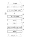
- the computer 64 starts the process when the liquid crystal panel 40 or the liquid crystal display device 10 including the liquid crystal panel 40 is set by the user to configure the correction system 1 and a correction instruction for the liquid crystal panel 40 is input from the user.
- the computer 64 first executes an initial correction process (S2).
- the computer 64 controls the signal source 62 and inputs the image data G to the supply circuit 12 (S12).
- the signal source 62 stores image data G for displaying a solid pattern of reference gradation values in advance, and when the signal source 62 receives a command from the computer 64, the image data G is supplied to the supply circuit 12.
- Send When the arithmetic circuit 22 receives the image data G from the signal source 62, the arithmetic circuit 22 functions as the supply unit 32, and supplies the image data G to the liquid crystal panel 40 in accordance with a command from the computer 64 (S14) to display the liquid crystal panel 40.
- the computer 64 controls the camera 66 to photograph the display area 42 when the liquid crystal panel 40 displays (S16), and transmits the photographing result W to the computer 64.
- correction data H1 means correction data generated by the computer 64.
- the photographing result W includes a photographing result corresponding to each pixel P of the liquid crystal panel 40, and the computer 64 detects the luminance variation B of the photographing result of each pixel P, and the luminance variation B is transmitted to the computer 64.
- Correction data H1 corresponding to each pixel P is generated so as to be within a pre-stored specified range KH.
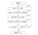
- the computer 64 executes a reading process for transmitting the correction data H1 from the computer 64 to the supply circuit 12 (S20). As shown in FIG. 8, in the reading process, the computer 64 transmits the correction data H1 to the supply circuit 12 (S62). When receiving the correction data H1, the arithmetic circuit 22 writes the correction data H1 into the DRAM 26 and stores it in the DRAM 26 (S64).
- the computer 64 transmits the same correction data H1 to the supply circuit 12 again when a predetermined time necessary for writing the correction data H1 has elapsed since the previous transmission of the correction data H1 (S66).
- the arithmetic circuit 22 reads the correction data H1 stored in the DRAM 26 (S68), and compares the correction data H1 received again with the correction data H1 read from the DRAM 26 (S70).
- the computer 64 ends the reading process.
- these two correction data H1 are different (S70: NO)
- the processing from S62 to S70 is repeated.
- the computer 64 executes a correction process (S22).
- the computer 64 controls the signal source 62 and inputs the image data G to the supply circuit 12.
- the arithmetic circuit 22 functions as the correction unit 34, reads the correction data H1 stored in the DRAM 26, corrects the image data G, and generates corrected image data G ′. .
- the arithmetic circuit 22 changes the correction data H ⁇ b> 1 stored in the DRAM 26 to the correction data H ⁇ b> 2 and ends the initial correction process.
- “correction data H2” means correction data stored in the DRAM 26 until the next correction processing after the correction processing, and means correction data used in the previous correction processing.
- the computer 64 After completing the initial correction process, the computer 64 functions as the control unit 72 and executes the re-correction process (S4). As shown in FIG. 5, in the recorrection process, the computer 64 controls the arithmetic circuit 22 to redisplay the liquid crystal panel 40. When receiving the command from the computer 64, the arithmetic circuit 22 functions as the supply unit 32, supplies the corrected image data G ′ generated in S22 to the liquid crystal panel 40 (S24), and redisplays the liquid crystal panel 40. The computer 64 images the display area 42 when the liquid crystal panel 40 displays (S26), and transmits the imaging result W ′ to the computer 64.
- the computer 64 generates new correction data H1 from the photographing result W ′ (S28), and transmits the correction data H1 to the supply circuit 12 (S30).
- These processes (S28, S30) in the re-correction process are the same processes as the processes of the same name (S18, S20) in the initial correction process, and redundant description is omitted.
- the arithmetic circuit 22 executes the addition process after the reading process (S30) for receiving the correction data H1 (S32).
- the arithmetic circuit 22 reads the correction data H1 and H2 stored in the DRAM 26 and adds them to generate the correction data H.
- the arithmetic circuit 22 writes the generated correction data H into the DRAM 26 and stores it in the DRAM 26 (S34).
- Correction data H correction data H1 + correction data H2
- correction data H is correction data generated again by adding correction data H1 newly generated this time to correction data H2 which is correction data used in the previous correction processing.
- correction can be made by adding the correction data H1 to the display unevenness that cannot be corrected by the correction data H2, and the correction accuracy is improved compared to the correction data H2. .
- the computer 64 executes a correction process (S36).
- the computer 64 controls the signal source 62 and inputs the image data G to the supply circuit 12.
- the arithmetic circuit 22 functions as the correction unit 34, reads the correction data H stored in the DRAM 26, corrects the image data G, and generates corrected image data G ′′.
- the re-correction process is finished.
- “corrected image data G ′′” is corrected image data generated using the corrected data H generated again, and can be said to be corrected image data generated again.
- the computer 64 executes determination processing after completing the re-correction processing (S6). As shown in FIG. 6, in the determination process, the computer 64 controls the arithmetic circuit 22 to redisplay the liquid crystal panel 40. When the arithmetic circuit 22 receives an instruction from the computer 64, the arithmetic circuit 22 functions as the supply unit 32, supplies the corrected image data G ′′ generated in S36 to the liquid crystal panel 40 (S42), and redisplays the liquid crystal panel 40. . The computer 64 images the display area 42 displayed on the liquid crystal panel 40 (S44), and transmits the imaging result W ′′ to the computer 64.
- the computer 64 Upon receiving the imaging result W ′′, the computer 64 detects the luminance variation B ′′ of the imaging result W ′′ and compares the detected luminance variation B ′′ with the specified range KH (S46). When the detected luminance variation B ′′ is within the specified range KH (S46: YES), the computer 64 ends the determination process. At this time, the computer 64 erases the correction data H and H1 stored in the DRAM 26. On the other hand, when the detected luminance variation B ′′ is larger than the specified range KH (S46: NO), the determination process is interrupted. The computer 64 returns to the re-correction process and executes the processes from S28 again.
- the computer 64 controls the arithmetic circuit 22 to erase the correction data H1 and H2 stored in the DRAM 26. Further, the computer 64 changes the correction data H stored in the DRAM 26 to the correction data H2.
- the computer 64 starts processing using the imaging result W ′′ captured in S44 as the imaging result W ′ captured in S26. That is, after returning to the recorrection process, the computer 64 executes the processes from S28 again without performing the processes of S24 and S26. That is, it is avoided that the display and photographing of the same corrected image data G ′′ are repeatedly performed in the determination step and the subsequent recorrection processing.
- the computer 64 executes a storage process (S8). As shown in FIG. 7, in the storage process, the computer 64 transmits the correction data H1 to the supply circuit 12 (S52), and executes an addition process (S54). These processes (S52, S54) of the storage process are the same processes as the processes of the same name (S30, S32) in the recorrection process, and a duplicate description is omitted.
- the computer 64 controls the arithmetic circuit 22 to execute a writing process for writing the correction data H into the FLASH memory 24 (S56).
- the arithmetic circuit 22 confirms whether or not the correction data H has been erased from the FLASH memory 24 in accordance with an instruction from the computer 64 (S82).
- the arithmetic circuit 22 keeps the correction data H already written in the FLASH memory 24 (S82: NO).
- the correction data H generated in S54 is written into the FLASH memory 24 and stored in the FLASH memory 24 (S86).
- the arithmetic circuit 22 When the arithmetic circuit 22 finishes writing the correction data H to the FLASH memory 24, the arithmetic circuit 22 reads the correction data H stored in the FLASH memory 24 (S88) and compares it with the correction data H stored in the DRAM 26 (S90). . When these two correction data H are equal (S90: YES), the computer 64 ends the writing process and ends the process. On the other hand, when these two correction data H are different (S90: NO), the processing from S82 to S90 is repeated.
- the corrected image data G ′ generated from the photographing result W is liquid crystal.
- the processes (S16 to S24, S26 to S42) until redisplayed on the panel 40 are repeatedly executed. While these processes are being executed, the correction data H (H1, H2) is a volatile storage device. Store in the DRAM 26. According to the correction system 1, the DRAM 26 is used as a storage device that stores the correction data H, so that the time required for processing can be shortened.
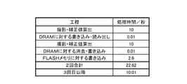
- FIG. 10 shows the time required for the processing of this embodiment.
- FIG. 11 shows the time required for correction processing when the conventional correction system is used, that is, when processing from acquisition of the imaging result W to redisplay of the liquid crystal panel 40 is executed using a nonvolatile storage device. Shown in comparison.
- the time required for these processes is shortened by replacing the time for writing and reading with respect to the DRAM 26 with the time for writing and reading with respect to the FLASH memory 24 of the prior art.
- the time required for these processes is shortened by replacing the time for erasing and writing with respect to the DRAM 26 with the time for erasing and writing with respect to the conventional FLASH memory 24. Therefore, in the correction process of the present embodiment, even when the process from the acquisition of the imaging result W to the redisplay of the liquid crystal panel 40 is repeatedly executed, the time required for the process can be reduced.
- the process of generating the correction data H is executed a plurality of times.
- noise may occur in the camera 66, or an imaging error due to a filter attached to the camera 66 may occur.
- a calculation error may occur, and a technique such as data compression is used to generate correction data as large as about 4 megabits in a short time. It is necessary to use this, and calculation errors may occur.
- even the correction data H generated through appropriate processing from the photographing result W may include an error, and the correction data H obtained by one generation processing accurately displays the display unevenness of the liquid crystal panel 40. It may not be possible to correct well.
- correction data H1 generated from the latest photographing result W and the DRAM 26 are stored in the previous correction processing.
- Correction data H is generated by adding the correction data H2 used, and correction processing is executed using the correction data H. Accordingly, it is possible to generate correction data H with higher accuracy by combining the correction data H generated a plurality of times, and display unevenness of the liquid crystal panel 40 can be corrected with high accuracy.
- the same correction data H1 is transmitted from the computer 64 to the supply circuit 12 twice, and the calculation circuit 22 to which the correction data H is input A so-called Verify operation is performed to check whether or not these correction data H1 match. That is, the Verify operation is executed in the device to which predetermined data is input. Accordingly, when a communication error occurs in transmission of the correction data H from the computer 64 to the supply circuit 12, generation of the corrected image data G ′ using the correction data H in which the communication error has occurred is suppressed, and the display is performed. The display unevenness of the panel can be corrected with high accuracy.
- the input line 18 to which the image data G is input to the supply circuit 12 and the input line 18 to which the correction data H is input to the supply circuit 12 are equal. Even when the image data G is sent using the input line 18 to which data whose transmission direction is determined in advance is transmitted, a communication error can be detected and display unevenness of the liquid crystal panel 40 can be corrected with high accuracy. Can do.
- the correction system 1 of the present embodiment has identification image data (identification symbol of the identification symbol) that informs the FLASH memory 24 of the supply circuit 12 of the occurrence of a communication error between the computer 64 and the supply circuit 12.
- identification image data identification symbol of the identification symbol
- K is stored. In the following description, the same description as that of the first embodiment will not be repeated.
- the arithmetic circuit 22 compares these two correction data H1 (S70).
- the correction data H1 is the identification image data K stored in the FLASH memory 24 as shown in FIG.
- Identification image data K for displaying “ ⁇ ”, which is an identification image indicating equality, is read and output to the liquid crystal panel 40 via the supply line 20 (S72). As a result, “ ⁇ ” is displayed on the liquid crystal panel 40.
- the arithmetic circuit 22 indicates that the correction data H1 is different among the identification image data K stored in the FLASH memory 24 as shown in FIG.
- the identification image data K for displaying “x”, which is an identification image indicating “”, is read and output to the liquid crystal panel 40 via the supply line 20 (S74). As a result, “x” is displayed on the liquid crystal panel 40.
- the computer 64 images the display area 42 when the identification image is displayed on the liquid crystal panel 40, and transmits the imaging result W ′ to the computer 64.
- the computer 64 confirms the photographing result W ′ and detects that “ ⁇ ” is included in the photographing result W ′, the reading process ends.
- the processing from S ⁇ b> 62 is repeated and the correction data H ⁇ b> 1 is supplied to the supply circuit 12 again.
- the computer 64 can detect the identification image using the camera 66, and between the computer 64 and the supply circuit 12. It is possible to detect that a communication error has occurred. When a communication error occurs, the computer 64 further supplies correction data H1 to the supply circuit 12, thereby generating corrected image data G ′ based on the correction data H1 input when the communication error occurs. It can be suppressed.
- a third embodiment will be described with reference to FIG.
- a plurality of conversion patterns C for converting correction data H1 input from the computer 64 to the supply circuit 12 are stored in the computer 64 as indicated by dotted lines in FIG. This is different from the correction system 1 of the first embodiment. In the following description, the same description as that of the first embodiment will not be repeated.
- the computer 64 converts the correction data H1 with the first conversion pattern C1 prior to inputting the correction data H1 to the supply circuit 12 at S62 (S61).
- the converted correction data H1 is input to the supply circuit 12.
- the correction data H1 Prior to inputting the correction data H1 to the supply circuit 12 in S66, the correction data H1 is converted with a second conversion pattern C2 different from the first conversion pattern C1 (S65), and the converted correction data H1 is supplied to the supply circuit. 12 is input.
- the arithmetic circuit 22 compares these two correction data H1 (S70).
- the arithmetic circuit 22 converts the correction data H1 received in S62 again based on the first conversion pattern C1. Further, the correction data H1 received in S66 is converted again based on the second conversion pattern C2. The arithmetic circuit 22 compares the two converted correction data H1 and checks whether they are equal.
- the computer 64 stores a plurality of conversion patterns C, and the correction data H1 input to the supply circuit 12 is converted using the conversion patterns C, whereby the computer 64 and the detection accuracy of a communication error occurring between the supply circuit 12 is improved.
- a communication error that occurs between the computer 64 and the supply circuit 12 includes a disconnection of the input line 18.
- correction data H ⁇ b> 1 in which all signals indicate “0” or “1” is input to the supply circuit 12.
- the arithmetic circuit 22 that has received the correction data H1 mistakenly indicates that no communication error has occurred because the correction data H1 received at different timings is the same although the input correction data H1 is incorrect. It will be detected.
- the computer 64 converts the correction data H1 using the first conversion pattern C1 and the second conversion pattern C2 that are different from each other. To do.
- the arithmetic circuit 22 reconverts the received correction data H1 using these conversion patterns C and checks whether they are equal. Therefore, even when the correction data H1 is equal when the arithmetic circuit 22 receives the correction data H1, if the reconverted correction data H1 is not equal, a communication error can be detected, and a communication error can be detected. Accuracy can be improved.
- the correction data H is generated based on the luminance variation B of the imaging result W, and the example of determining whether to end the determination process has been described. Is not limited to this.
- the processing may be performed based on the chromaticity variation together with the luminance variation B of the photographing result W.
- the DRAM 26 may be provided inside the arithmetic circuit 22.
- the process in which the arithmetic circuit 22 writes the correction data H to the DRAM 26 is an internal process of the arithmetic circuit 22, and the time required for the process performed in the correction system 1 may be further shortened.
- the embodiment of the invention is not limited to this.
- a test result may be output using a connection line connected to a serial communication bus such as I2C.
- the data output as the inspection result is not limited to the identification image data K, and is appropriately changed to a necessary form.
- the identification image data K is output to the liquid crystal panel 40 via the supply line 20, the identification image is not limited to “ ⁇ ” or “ ⁇ ”. Furthermore, it is not necessary to be “image data”. For example, any process that can be recognized by the camera 66, such as reducing the brightness of the backlight unit 50, may be used.
- the light source using the LED as the light source is exemplified, but a light source other than the LED may be used.
- correction system 10: liquid crystal display device, 12: supply circuit, 14: display unit, 18: input line, 20: supply line, 22: arithmetic circuit, 24: FLASH memory, 26: DRAM, 32: supply unit, 34: correction unit, 40: liquid crystal panel, 42: display area, 62: signal source, 64: computer, 66: camera, 70: generation unit, 72: control unit, B: luminance variation, G: image data, G ′ , G ′′: correction image data, H, H1, H2: correction data, KH: specified range, W: photographing result, C: conversion pattern, K: identification image data
Landscapes
- Engineering & Computer Science (AREA)
- Physics & Mathematics (AREA)
- Computer Hardware Design (AREA)
- General Physics & Mathematics (AREA)
- Theoretical Computer Science (AREA)
- Control Of Indicators Other Than Cathode Ray Tubes (AREA)
- Liquid Crystal Display Device Control (AREA)
Abstract
A process according to the present invention which corrects display unevenness of a liquid-crystal panel (40) comprises the following steps: 1. Supply image data to the liquid-crystal panel (40) and display the image data on the liquid-crystal panel (40); 2. Photograph a display region of the liquid-crystal panel (40) with a camera (66); 3. Generate correction data of the liquid-crystal panel (40) from a result of the photography; 4. Store the correction data on a non-volatile storage device; 5. Generate corrected image data using the correction data which is stored on the non-volatile storage device; 6. Supply the corrected image data to the liquid-crystal panel (40) and re-display the corrected image data on the liquid-crystal panel (40); and 7. Repeat the execution of steps 2-6.
Description
本発明は、表示パネルのムラ補正方法及び補正システムに関し、特に表示パネルの表示ムラを補正する技術に関する。
The present invention relates to a display panel unevenness correction method and correction system, and more particularly, to a technique for correcting display panel unevenness.
近年、大画面テレビジョンなどの高性能な表示装置が普及しつつある。これらの表示装置においては、表示画像に発生する輝度ムラや色ムラ(以後、輝度ムラと色ムラをあわせて「表示ムラ」と呼ぶことがある)が画質に大きな影響を与えるため、表示ムラを適切に補正することが必要となる。
In recent years, high-performance display devices such as large-screen televisions are becoming widespread. In these display devices, luminance unevenness and color unevenness that occurs in a display image (hereinafter, luminance unevenness and color unevenness may be referred to as “display unevenness”) greatly affect image quality. It is necessary to correct appropriately.
従来から、表示ムラを補正する技術が開示されている(例えば、特許文献1)。従来技術の補正装置では、表示パネルに表示された映像を、撮影装置を用いて撮影し、撮影した結果に基づいて補正データを生成し、この補正データを不揮発性記憶装置に書き込んでおく。そして、画像データを補正する際には、補正装置の不揮発性記憶装置から補正データを読み出し、当該補正データを用いて画像データを補正する。
Conventionally, a technique for correcting display unevenness has been disclosed (for example, Patent Document 1). In the correction device of the prior art, an image displayed on the display panel is shot using a shooting device, correction data is generated based on the shooting result, and the correction data is written in the nonvolatile storage device. When correcting the image data, the correction data is read from the nonvolatile storage device of the correction device, and the image data is corrected using the correction data.
(発明が解決しようとする課題)
補正データでは、当該補正データが用いられる表示パネルを撮影した結果に基づいて生成されたとしても、撮影時のノイズや、補正データ生成時の演算誤差、あるいは補正データ生成時のデータ圧縮等の原因で、補正データの精度が低下してしまうことがある。補正データの精度を向上させるためには、補正データを用いてさらに表示パネルを撮影し、補正データを生成するなど、補正データを繰り返し生成することが有効である。しかし、補正データが不揮発性記憶装置に書き込まれている場合、補正データの消去や書き込みに比較的長い時間が必要となり、補正データを繰り返し生成することが難しい。 (Problems to be solved by the invention)
Even if the correction data is generated based on the result of shooting the display panel in which the correction data is used, the cause of noise during shooting, calculation error when generating correction data, or data compression when generating correction data, etc. As a result, the accuracy of the correction data may be reduced. In order to improve the accuracy of the correction data, it is effective to repeatedly generate the correction data, for example, by photographing the display panel using the correction data and generating the correction data. However, when the correction data is written in the nonvolatile storage device, it takes a relatively long time to erase and write the correction data, and it is difficult to generate the correction data repeatedly.
本発明は、このような状況に鑑みてなされたものであり、表示パネルのムラ補正に必要な時間を短縮することを目的とする。
The present invention has been made in view of such a situation, and an object thereof is to reduce the time required for correcting the unevenness of the display panel.
(課題を解決するための手段)
上記課題を解決するために、本発明は、表示パネルの表示ムラを補正する表示パネルのムラ補正方法であって、前記表示パネルに画像データを供給して当該表示パネルを表示させる供給工程と、表示された前記表示パネルの表示領域を撮影する撮影工程と、前記撮影工程の撮影結果から前記表示パネルの補正データを生成する生成工程と、前記補正データを揮発性記憶装置に記憶する記憶工程と、前記揮発性記憶装置に記憶された前記補正データを用いて前記画像データを補正して補正画像データを生成する補正工程と、前記表示パネルに前記補正画像データを供給して当該表示パネルを再表示させる再供給工程と、前記撮影工程から前記再供給工程までの工程を繰り返し実行する繰返工程と、を含むことを特徴とする。 (Means for solving problems)
In order to solve the above-mentioned problem, the present invention is a display panel unevenness correction method for correcting display unevenness of a display panel, and includes a supplying step of supplying image data to the display panel to display the display panel; A photographing step of photographing the displayed display area of the display panel; a generating step of generating correction data of the display panel from a photographing result of the photographing step; and a storage step of storing the correction data in a volatile storage device; A correction step of correcting the image data using the correction data stored in the volatile storage device to generate corrected image data; supplying the corrected image data to the display panel; A re-feeding step for displaying, and a repeating step for repeatedly executing the steps from the photographing step to the re-feeding step.
この表示パネルのムラ補正方法では、撮影工程から再供給工程までの工程を繰り返し実行し、これによって得られた補正データを揮発性記憶装置に記憶する。この表示パネルの駆動方法によれば、補正データを記憶する記憶装置として揮発性記憶装置を用いることで、不揮発性記憶装置を用いる場合に比べて、補正データを記憶装置に書き込む時間や、補正データを記憶装置から消去する時間等の各種時間を短縮することができ、撮影工程から再供給工程までの工程を繰り返し、補正データの消去や書き込みを複数回に亘って実行した場合でも、表示パネルのムラ補正に必要な時間を短縮することができる。
In this display panel unevenness correction method, the steps from the photographing step to the resupply step are repeatedly executed, and the correction data obtained thereby is stored in the volatile storage device. According to this display panel driving method, by using a volatile storage device as a storage device for storing the correction data, the time for writing the correction data in the storage device and the correction data are compared with the case of using the nonvolatile storage device. Various times such as the time to erase the data from the storage device can be shortened, and even if the correction data is erased and written multiple times by repeating the steps from the photographing process to the resupply process, the display panel The time required for unevenness correction can be shortened.
前記繰返工程に含まれる生成工程では、当該繰返工程に含まれる撮影工程の撮影結果から生成される第1補正データと、前回の生成工程で生成された補正データである第2補正データと、を足し合わせることで前記補正データを生成することが好ましい。これによって、複数回の補正工程で生成される補正データを合成したより高精度な補正データを生成することができ、表示ムラを精度良く補正することができる。
In the generation step included in the repetition step, first correction data generated from the imaging result of the imaging step included in the repetition step, and second correction data that is correction data generated in the previous generation step, Preferably, the correction data is generated by adding together. Accordingly, it is possible to generate correction data with higher accuracy by combining correction data generated in a plurality of correction steps, and display unevenness can be corrected with high accuracy.
前記画像データは、前記表示パネルの全表示領域において同一の輝度及び色度情報を有する画像データであり、前記生成回路は、前記撮影結果のバラツキが予め定められた規定範囲内となるように前記第1補正データを生成することが好ましい。これによって、例えば、階調ベタパターンを表示した場合の撮影結果のバラツキを、人の視覚等を基準として定められた規定範囲内となるよう第1補正データを生成することで、表示ムラを精度良く補正することができる。
The image data is image data having the same luminance and chromaticity information in the entire display area of the display panel, and the generation circuit is configured so that a variation in the photographing result is within a predetermined specified range. It is preferable to generate the first correction data. As a result, for example, the first correction data is generated so that the variation in the photographing result when the gradation solid pattern is displayed is within a specified range determined based on human vision or the like, thereby accurately displaying unevenness. It can be corrected well.
前記繰返工程を実行するか否かを決定する決定工程をさらに含んでいても良い。この場合、前記決定工程は、前記繰返工程実行後、再び繰返工程を実行するに先立って実行されることが好ましい。
It may further include a determining step for determining whether or not to execute the repeating step. In this case, it is preferable that the determination step is executed prior to executing the repetition step again after the execution of the repetition step.
この表示パネルのムラ補正方法では、繰返工程を実行するか否かを決定する決定工程を備えている。そのため、1度の繰返工程で十分な補正画像データを生成することができる場合、つまり1度の繰返工程を経て生成される補正画像データを用いて表示ムラを精度良く補正することができる場合には、2度、3度の繰返工程を実行することが抑制され、表示パネルのムラ補正に必要な時間を短縮することができる。
This unevenness correction method for a display panel includes a determining step for determining whether or not to execute a repeating step. Therefore, when sufficient correction image data can be generated in one repeating process, that is, display unevenness can be corrected with high accuracy using the corrected image data generated through one repeating process. In this case, it is possible to reduce the time required for correcting the unevenness of the display panel by suppressing the second and third repeated steps.
前記決定工程は、前記撮影工程を含んでおり、当該撮影工程における撮影結果のバラツキが前記規定範囲内である場合、前記繰返工程を実行しないと決定し、前記バラツキが前記規定範囲よりも大きい場合、前記繰返工程を実行すると決定し、前記決定工程後に前記繰返工程が実行される場合、前記決定工程に含まれる撮影工程は、前記繰返工程の撮影工程を兼ねることが好ましい。
The determining step includes the photographing step, and when the variation in the photographing result in the photographing step is within the specified range, it is determined that the repeating step is not performed, and the variation is larger than the predetermined range. In this case, when it is determined that the repetition process is to be executed and the repetition process is executed after the determination process, it is preferable that the imaging process included in the determination process also serves as the imaging process of the repetition process.
この表示パネルのムラ補正方法によれば、決定工程において撮影結果のバラツキが規定範囲よりも大きいと判断され、決定工程後に繰返工程が実行される場合に、決定工程と繰返工程において、同一の撮影工程が続けて行われることが抑制され、表示パネルのムラ補正に必要な時間を短縮することができる。
According to this unevenness correction method for a display panel, when it is determined that the variation in the photographing result is larger than the specified range in the determination step, and the repetition step is executed after the determination step, the same in the determination step and the repetition step. Thus, it is possible to reduce the time required for correcting the unevenness of the display panel.
前記供給工程は、液晶を用いた液晶パネルを用いて行われることが好ましい。これによって、大画面テレビジョン等に用いられる液晶パネルの表示ムラを精度良く抑制することができる。
The supply step is preferably performed using a liquid crystal panel using liquid crystal. Thereby, display unevenness of a liquid crystal panel used for a large screen television or the like can be suppressed with high accuracy.
本発明は、上記のムラ補正方法を実現する補正システムにも具現化される。本発明は、表示パネルの表示ムラを補正する補正システムであって、表示パネルに画像データを供給して当該表示パネルを表示させる供給部と、前記表示パネルの表示領域を撮影する撮影部と、前記撮影装置の撮影結果から前記表示パネルの補正データを生成する生成部と、前記補正データを記憶する揮発性の記憶部と、前記記憶部に記憶された前記補正データを用いて前記画像データを補正した補正画像データを生成する補正部と、前記表示パネルに前記補正画像データを供給して当該表示パネルを表示させた際に撮影された撮影結果から再度の補正データを生成し、当該再度の補正データから再度の補正画像データを生成するように、前記各部を制御する制御部と、を備えることを特徴とする。
The present invention is also embodied in a correction system that realizes the above-described unevenness correction method. The present invention is a correction system that corrects display unevenness of a display panel, a supply unit that supplies image data to the display panel and displays the display panel, a photographing unit that captures a display area of the display panel, Using the correction data stored in the storage unit, a generation unit that generates correction data of the display panel from the imaging result of the imaging device, the volatile storage unit that stores the correction data, and the image data A correction unit that generates corrected image data that has been corrected, and the correction image data supplied to the display panel to generate correction data again from the shooting result that was shot when the display panel was displayed. And a control unit that controls each of the units so as to generate corrected image data again from the correction data.
この表示装置では、生成部が補正データを生成し、その補正データを用いて再度生成部が生成した補正データから生成された補正画像データが表示パネルに表示される。つまり、最終的に生成される補正画像データは、補正部によって複数回補正されている。この補正システムによれば、記憶部として揮発性の記憶部を用いることで、不揮発性の記憶部を用いる場合に比べて各種時間を短縮することができ、補正部によって複数回補正が実行された場合でも、表示パネルのムラ補正に必要な時間を短縮することができる。
In this display device, the generation unit generates correction data, and the corrected image data generated from the correction data generated by the generation unit again using the correction data is displayed on the display panel. That is, the corrected image data finally generated is corrected a plurality of times by the correction unit. According to this correction system, by using a volatile storage unit as the storage unit, various times can be shortened compared to the case of using a non-volatile storage unit, and the correction unit has performed correction multiple times. Even in this case, the time required for correcting the unevenness of the display panel can be shortened.
前記生成部は、生成した前記補正データを前記補正部に入力するとともに、当該補正データを前記補正部に入力する際には複数回に亘って同一の前記補正データを入力しており、前記補正部は、異なるタイミングに入力される前記補正データが一致するか否かを検査することが好ましい。
The generation unit inputs the generated correction data to the correction unit, and inputs the same correction data multiple times when the correction data is input to the correction unit. The unit preferably checks whether or not the correction data input at different timings match.
この補正システムでは、補正データが入力される補正部において、異なるタイミングに入力される補正データが一致するか否かを検査する。つまり、通信エラーに伴う書き込み不一致を検査する、いわゆるVerify作業を実行する。この補正システムによれば、例えば補正部に対する補正データのように、外部から入力されるのみで、外部に対して出力されることがないデータに対する通信エラーを検出することができる。これによって、通信エラーが発生した補正データを用いて補正画像データが生成されることが抑制され、表示パネルの表示ムラを精度良く補正することができる。
In this correction system, the correction unit to which correction data is input checks whether the correction data input at different timings match. That is, a so-called Verify operation is performed to check for a write mismatch associated with a communication error. According to this correction system, it is possible to detect a communication error for data that is only input from the outside and is not output to the outside, such as correction data for the correction unit. Accordingly, generation of corrected image data using the correction data in which a communication error has occurred is suppressed, and display unevenness of the display panel can be corrected with high accuracy.
前記生成部は、前記補正部に前記画像データが入力される入力ラインと、前記補正データを前記補正部に入力する入力ラインは等しいことが好ましい。これによって、補正データを、例えば画像データように、伝達方向が予め決定されているデータが入力される入力ラインを用いて送る場合でも通信エラーを検出することができ、表示パネルの表示ムラを精度良く補正することができる。
Preferably, in the generation unit, an input line through which the image data is input to the correction unit and an input line through which the correction data is input to the correction unit are the same. As a result, communication errors can be detected even when correction data is sent using an input line to which data whose transmission direction is determined in advance, such as image data, is input, and display unevenness of the display panel can be accurately detected. It can be corrected well.
前記補正部は、前記補正データを検査した検査結果を出力する出力ラインを接続可能に構成されていることが好ましい。これによって、出力ラインを用いて補正部が補正データ検査結果を検査した検査結果を補正部の外部に読み出すことができ、当該検査結果を補正システムの処理に反映させることができる。
It is preferable that the correction unit is configured to be connectable to an output line that outputs an inspection result obtained by inspecting the correction data. As a result, the inspection result obtained by inspecting the correction data inspection result by the correction unit using the output line can be read out of the correction unit, and the inspection result can be reflected in the processing of the correction system.
前記出力ラインは、前記表示パネルに前記補正画像データを供給する供給ラインと等しく、前記補正部は、前記検査結果を示す識別記号を有しており、前記検査結果に応じて前記識別記号を前記表示パネルに出力しており、前記生成部は、前記撮影結果に前記補正データが一致しないことを示す識別記号が含まれることを検出した場合に、前記補正データを前記補正部に再度入力することが好ましい。
The output line is equal to a supply line that supplies the corrected image data to the display panel, and the correction unit has an identification symbol indicating the inspection result, and the identification symbol is set according to the inspection result. Output to the display panel, and when the generation unit detects that an identification symbol indicating that the correction data does not match is included in the photographing result, the generation unit inputs the correction data to the correction unit again. Is preferred.
この表示装置では、表示パネルに識別記号を表示することで、補正データの検査結果を補正部の外部に出力する。生成部は、撮影部を介して入力された撮影画像を確認し、撮影画像に補正データが一致しないことを示す識別記号が含まれていることを検出した場合に、再度、補正部に補正データを入力する。これによって、通信エラーが発生した際に入力された補正データに基づいて補正画像データが生成されることを抑制することができる。
This display device outputs an inspection result of correction data to the outside of the correction unit by displaying an identification symbol on the display panel. When the generation unit confirms the captured image input via the imaging unit and detects that the captured image includes an identification symbol indicating that the correction data does not match, the generation unit again corrects the correction data to the correction unit. Enter. Thereby, it is possible to suppress generation of corrected image data based on correction data input when a communication error occurs.
前記生成部は、前記補正データを変換する複数の変換パターンを有しており、同一の前記補正データを前記補正部に複数回に亘って入力する際には、少なくとも2つの前記変換パターンで変換された前記補正データを前記補正部に入力することが好ましい。
The generation unit has a plurality of conversion patterns for converting the correction data, and when the same correction data is input to the correction unit a plurality of times, conversion is performed using at least two conversion patterns. It is preferable to input the corrected data to the correction unit.
例えば、通信エラーとして入力ラインに断線が発生した場合、生成部から出力される補正データに関わらず補正部に入力される補正データは全て同じとなり、補正部に入力される複数の補正データを用いて通信エラーを検出することができない。この表示装置では、生成部から補正部に補正データを入力する際に、生成部で複数の変換パターンを用いて補正データを変換し、補正部は複数の変換パターンで変換された補正データを用いて検査を行う。そのため、例えば、入力ラインに断線が発生し、複数の変換パターンで変換されたにも関わらず、補正部に同一の補正データが入力された場合には、通信エラーが発生していることを検出することができ、通信エラーの検出精度を向上させることができる。
For example, when a disconnection occurs in the input line as a communication error, all the correction data input to the correction unit is the same regardless of the correction data output from the generation unit, and a plurality of correction data input to the correction unit is used. Communication error cannot be detected. In this display device, when the correction data is input from the generation unit to the correction unit, the generation unit converts the correction data using a plurality of conversion patterns, and the correction unit uses the correction data converted by the plurality of conversion patterns. Inspect. Therefore, for example, if the same correction data is input to the correction unit even though the input line is disconnected and converted using multiple conversion patterns, it is detected that a communication error has occurred. It is possible to improve communication error detection accuracy.
前記補正データを記憶する不揮発性の第2記憶部をさらに備えていてもよい。この場合、前記制御部は、前記再度の補正データ及び再度の補正画像データを生成後、前記表示部及び前記撮影部を制御して当該再度の補正画像データを前記表示パネルに表示させた場合の撮影結果を取得しており、当該撮影結果のバラツキが予め定められた規定範囲よりも大きい場合、前記生成部及び前記補正部を制御して当該撮影結果から新たな再度の補正画像データを生成しており、当該撮影結果のバラツキが前記規定範囲内である場合、前記生成部及び前記補正部を制御して前記再度の補正データを前記生成部から前記補正部に入力し、さらに前記補正部から前記第2記憶部に記憶しており、前記生成部は、前記撮影結果のバラツキが前記規定範囲内である場合、前記再度の補正データを前記補正部に複数回に亘って入力することが好ましい。
A non-volatile second storage unit that stores the correction data may be further provided. In this case, the control unit generates the second correction data and the second corrected image data, and then controls the display unit and the photographing unit to display the second corrected image data on the display panel. When the shooting result is acquired and the variation of the shooting result is larger than a predetermined range, the generation unit and the correction unit are controlled to generate new corrected image data from the shooting result. When the variation in the photographing result is within the specified range, the generation unit and the correction unit are controlled to input the second correction data from the generation unit to the correction unit, and from the correction unit The generation unit stores the second correction data in the correction unit a plurality of times when the variation in the photographing result is within the specified range. Masui.
この補正システムでは、撮影結果のバラツキが規定範囲内となる補正データが生成された場合に、当該補正データに対してVerify作業を実行する。この補正システムによれば、撮影結果のバラツキが規定範囲内となる補正データに通信エラーが発生することが抑制され、表示パネルの表示ムラを精度良く補正することができる。
In this correction system, when correction data in which the variation in the photographing result is within the specified range is generated, the verification work is executed on the correction data. According to this correction system, it is possible to suppress occurrence of a communication error in the correction data in which the variation in the photographing result is within the specified range, and it is possible to accurately correct the display unevenness of the display panel.
(発明の効果)
本発明によれば、表示パネルのムラ補正に必要な時間を短縮することができる。 (The invention's effect)
According to the present invention, it is possible to reduce the time required for correcting the unevenness of the display panel.
本発明によれば、表示パネルのムラ補正に必要な時間を短縮することができる。 (The invention's effect)
According to the present invention, it is possible to reduce the time required for correcting the unevenness of the display panel.
<実施形態1>
実施形態1を、図面を参照して説明する。なお、以下の実施形態では、表示装置として液晶パネルを備える液晶表示装置を用いて説明を行う。しかしながら、本発明が適用可能な表示装置はこれに限られるものではなく、例えばPDP(プラズマディスプレイパネル)表示装置や、有機EL(エレクトロルミネッセンス)表示装置等のアクティブマトリックス型表示装置にも適用可能である。 <Embodiment 1>
The first embodiment will be described with reference to the drawings. In the following embodiments, description will be made using a liquid crystal display device including a liquid crystal panel as the display device. However, the display device to which the present invention can be applied is not limited to this, and can also be applied to an active matrix display device such as a PDP (plasma display panel) display device or an organic EL (electroluminescence) display device. is there.
実施形態1を、図面を参照して説明する。なお、以下の実施形態では、表示装置として液晶パネルを備える液晶表示装置を用いて説明を行う。しかしながら、本発明が適用可能な表示装置はこれに限られるものではなく、例えばPDP(プラズマディスプレイパネル)表示装置や、有機EL(エレクトロルミネッセンス)表示装置等のアクティブマトリックス型表示装置にも適用可能である。 <
The first embodiment will be described with reference to the drawings. In the following embodiments, description will be made using a liquid crystal display device including a liquid crystal panel as the display device. However, the display device to which the present invention can be applied is not limited to this, and can also be applied to an active matrix display device such as a PDP (plasma display panel) display device or an organic EL (electroluminescence) display device. is there.
1. 補正システムの構成
図1を用いて、液晶表示装置10の表示ムラを補正する補正システム1の構成を説明する。図1に示すように、本システム1は、液晶表示装置10と信号源62とコンピュータ64とカメラ(撮影部の一例)66を含む。液晶表示装置10は、後述するように、供給回路12と液晶パネル(表示パネルの一例)40を備えており、信号源62に入力ライン18を介して接続されている。供給回路12は、信号源62から送信される画像データGを、供給ライン20を介して液晶パネル40に供給し、液晶パネル40の表示領域42に表示する。カメラ66は、液晶パネル40の正面にカメラ66が配置されており、液晶パネル40の表示領域42を撮影する。 1. Configuration of Correction System The configuration of thecorrection system 1 that corrects display unevenness of the liquid crystal display device 10 will be described with reference to FIG. As shown in FIG. 1, the system 1 includes a liquid crystal display device 10, a signal source 62, a computer 64, and a camera (an example of a photographing unit) 66. As will be described later, the liquid crystal display device 10 includes a supply circuit 12 and a liquid crystal panel (an example of a display panel) 40, and is connected to a signal source 62 via an input line 18. The supply circuit 12 supplies the image data G transmitted from the signal source 62 to the liquid crystal panel 40 via the supply line 20 and displays it on the display area 42 of the liquid crystal panel 40. The camera 66 is disposed in front of the liquid crystal panel 40 and photographs the display area 42 of the liquid crystal panel 40.
図1を用いて、液晶表示装置10の表示ムラを補正する補正システム1の構成を説明する。図1に示すように、本システム1は、液晶表示装置10と信号源62とコンピュータ64とカメラ(撮影部の一例)66を含む。液晶表示装置10は、後述するように、供給回路12と液晶パネル(表示パネルの一例)40を備えており、信号源62に入力ライン18を介して接続されている。供給回路12は、信号源62から送信される画像データGを、供給ライン20を介して液晶パネル40に供給し、液晶パネル40の表示領域42に表示する。カメラ66は、液晶パネル40の正面にカメラ66が配置されており、液晶パネル40の表示領域42を撮影する。 1. Configuration of Correction System The configuration of the
コンピュータ64は、信号源62、カメラ66、及び液晶表示装置10の供給回路12に接続されている。コンピュータ64の内部には、補正システム1の各構成要素を制御するための各種のプログラムP1が記憶されており、コンピュータ64はこのプログラムP1に従って、制御部72として機能し、信号源62、カメラ66、供給回路12、及びコンピュータ64自身を制御する。
The computer 64 is connected to the signal source 62, the camera 66, and the supply circuit 12 of the liquid crystal display device 10. Various programs P1 for controlling each component of the correction system 1 are stored in the computer 64. The computer 64 functions as a control unit 72 according to the program P1, and includes a signal source 62 and a camera 66. , Control the supply circuit 12 and the computer 64 itself.
コンピュータ64には、カメラ66が撮影した撮影結果Wが送信されており、当該撮影結果Wから液晶パネル40の補正データHを生成する。この際、コンピュータ64は、撮影結果Wから補正データHを生成する生成部70として機能する。コンピュータ64は、生成した補正データHを供給回路12に入力する。この際、コンピュータ64は、信号源62を介して補正データHを供給回路12に送信しており、供給回路12に画像データGが送信される入力ライン18と、供給回路12に補正データHが送信される入力ライン18は等しい。
The photographing result W photographed by the camera 66 is transmitted to the computer 64, and the correction data H of the liquid crystal panel 40 is generated from the photographing result W. At this time, the computer 64 functions as a generation unit 70 that generates the correction data H from the imaging result W. The computer 64 inputs the generated correction data H to the supply circuit 12. At this time, the computer 64 transmits correction data H to the supply circuit 12 via the signal source 62, the input line 18 through which the image data G is transmitted to the supply circuit 12, and the correction data H to the supply circuit 12. The input lines 18 transmitted are equal.
図2に、液晶表示装置10の構成を示す。液晶表示装置10は、供給回路12と表示部14とバックライト駆動回路16を含む。表示部14は、液晶パネル40とバックライトユニット50を含んで構成されている。
FIG. 2 shows the configuration of the liquid crystal display device 10. The liquid crystal display device 10 includes a supply circuit 12, a display unit 14, and a backlight drive circuit 16. The display unit 14 includes a liquid crystal panel 40 and a backlight unit 50.
バックライトユニット50は、液晶パネル40の背面に配置されている。バックライトユニット50は、光源であるLED54(Light Emitting Diode:発光ダイオード)と、導光板52を備えている。LED54は、導光板52の側面に対向して配置されている。導光板52は、その主面52Aが液晶パネル40に対向して配置されている。導光板52では、LED54から側面52Bに入射された光を液晶パネル40に対向する主面52Aに導光している。そのため、導光板52の側面は、LED54から照射された光を導光板52内に取り込む入光面52Bとして機能している。また導光板52の主面は、導光板52内を導光した光を液晶パネル40へと照射する出光面52Aとして機能している。このようにバックライトユニット50は、その長辺側の両端部にLED54が配置され、その中央に導光板52を配してなる、いわゆるエッジライト型(サイドライト型)とされている。
The backlight unit 50 is disposed on the back surface of the liquid crystal panel 40. The backlight unit 50 includes an LED 54 (Light Emitting Diode), which is a light source, and a light guide plate 52. The LED 54 is disposed to face the side surface of the light guide plate 52. The light guide plate 52 is disposed so that its main surface 52A faces the liquid crystal panel 40. In the light guide plate 52, the light incident on the side surface 52 </ b> B from the LED 54 is guided to the main surface 52 </ b> A facing the liquid crystal panel 40. Therefore, the side surface of the light guide plate 52 functions as a light incident surface 52 </ b> B that takes light emitted from the LEDs 54 into the light guide plate 52. The main surface of the light guide plate 52 functions as a light output surface 52 </ b> A that irradiates the liquid crystal panel 40 with light guided through the light guide plate 52. Thus, the backlight unit 50 is of a so-called edge light type (side light type) in which the LEDs 54 are arranged at both ends on the long side and the light guide plate 52 is arranged at the center thereof.
バックライト駆動回路16は、バックライトユニット50を構成するLED54に接続されている。バックライト駆動回路16は各LED54に電流を供給しており、供給する電流量を制御することによって、各LED54から導光板52に入光される光量を制御している。
The backlight drive circuit 16 is connected to the LEDs 54 constituting the backlight unit 50. The backlight drive circuit 16 supplies current to each LED 54, and controls the amount of light incident on the light guide plate 52 from each LED 54 by controlling the amount of current supplied.
供給回路12は、演算回路22とFLASHメモリ24とDRAM(記憶部の一例)26を備える。FLASHメモリ24は、不揮発性の記憶装置であり、演算回路22の動作を制御するための各種のプログラムP2が記憶されている。演算回路22は、FLASHメモリ24から読み出したプログラムP2に従って、又はコンピュータ64から入力される命令に従って動作を行う。DRAM26は、揮発性の記憶装置であり、コンピュータ64から送信される補正データHを記憶する。
The supply circuit 12 includes an arithmetic circuit 22, a FLASH memory 24, and a DRAM (an example of a storage unit) 26. The FLASH memory 24 is a nonvolatile storage device and stores various programs P2 for controlling the operation of the arithmetic circuit 22. The arithmetic circuit 22 operates according to the program P2 read from the FLASH memory 24 or according to a command input from the computer 64. The DRAM 26 is a volatile storage device and stores correction data H transmitted from the computer 64.
演算回路22は、信号源62から画像データGが送信されており、供給部32として機能し、当該画像データGを液晶パネル40に供給し、液晶パネル40を表示させている。また、演算回路22は、DRAM26に補正データHが記憶されている場合には、DRAM26から補正データHを読み出し、当該補正データHを用いて信号源62から送信される画像データGを補正し、補正後の画像データG’を液晶パネル40に供給する。この際、演算回路22は、DRAM26から読み出した補正データHを用いて画像データGを補正し、補正後の画像データG’を生成する補正部34として機能する。
The arithmetic circuit 22 receives image data G from the signal source 62, functions as a supply unit 32, supplies the image data G to the liquid crystal panel 40, and displays the liquid crystal panel 40. When the correction data H is stored in the DRAM 26, the arithmetic circuit 22 reads the correction data H from the DRAM 26, corrects the image data G transmitted from the signal source 62 using the correction data H, The corrected image data G ′ is supplied to the liquid crystal panel 40. At this time, the arithmetic circuit 22 functions as the correction unit 34 that corrects the image data G using the correction data H read from the DRAM 26 and generates corrected image data G ′.
2.補正システムの処理
図3ないし図9を用いて、補正システム1における液晶パネル40の表示ムラを補正する処理について説明する。なお、当該処置の開始に先立って、供給回路12のDRAM26から補正データHは消去されているものとする。 2. Processing of Correction System Processing for correcting display unevenness of theliquid crystal panel 40 in the correction system 1 will be described with reference to FIGS. 3 to 9. It is assumed that the correction data H has been erased from the DRAM 26 of the supply circuit 12 prior to the start of the treatment.
図3ないし図9を用いて、補正システム1における液晶パネル40の表示ムラを補正する処理について説明する。なお、当該処置の開始に先立って、供給回路12のDRAM26から補正データHは消去されているものとする。 2. Processing of Correction System Processing for correcting display unevenness of the
コンピュータ64は、ユーザによって液晶パネル40、あるいは液晶パネル40を含む液晶表示装置10がセットされて補正システム1が構成され、ユーザから液晶パネル40の補正指示が入力されると、処理を開始する。コンピュータ64は、処理を開始すると、まず初期補正処理を実行する(S2)。
The computer 64 starts the process when the liquid crystal panel 40 or the liquid crystal display device 10 including the liquid crystal panel 40 is set by the user to configure the correction system 1 and a correction instruction for the liquid crystal panel 40 is input from the user. When starting the process, the computer 64 first executes an initial correction process (S2).
(初期補正処理)
図4に示すように、初期補正処理において、コンピュータ64は、信号源62を制御し、供給回路12に画像データGを入力する(S12)。信号源62には、予め基準階調値のベタパターンを表示するための画像データGが記憶されており、信号源62は、コンピュータ64からの命令を受信すると、供給回路12に当該画像データGを送信する。演算回路22は、信号源62から画像データGを受信すると、供給部32として機能し、コンピュータ64からの命令に従って当該画像データGを液晶パネル40に供給し(S14)、液晶パネル40を表示させる。コンピュータ64は、カメラ66を制御し、液晶パネル40が表示した際の表示領域42を撮影し(S16)、その撮影結果Wをコンピュータ64に送信する。 (Initial correction processing)
As shown in FIG. 4, in the initial correction process, thecomputer 64 controls the signal source 62 and inputs the image data G to the supply circuit 12 (S12). The signal source 62 stores image data G for displaying a solid pattern of reference gradation values in advance, and when the signal source 62 receives a command from the computer 64, the image data G is supplied to the supply circuit 12. Send. When the arithmetic circuit 22 receives the image data G from the signal source 62, the arithmetic circuit 22 functions as the supply unit 32, and supplies the image data G to the liquid crystal panel 40 in accordance with a command from the computer 64 (S14) to display the liquid crystal panel 40. . The computer 64 controls the camera 66 to photograph the display area 42 when the liquid crystal panel 40 displays (S16), and transmits the photographing result W to the computer 64.
図4に示すように、初期補正処理において、コンピュータ64は、信号源62を制御し、供給回路12に画像データGを入力する(S12)。信号源62には、予め基準階調値のベタパターンを表示するための画像データGが記憶されており、信号源62は、コンピュータ64からの命令を受信すると、供給回路12に当該画像データGを送信する。演算回路22は、信号源62から画像データGを受信すると、供給部32として機能し、コンピュータ64からの命令に従って当該画像データGを液晶パネル40に供給し(S14)、液晶パネル40を表示させる。コンピュータ64は、カメラ66を制御し、液晶パネル40が表示した際の表示領域42を撮影し(S16)、その撮影結果Wをコンピュータ64に送信する。 (Initial correction processing)
As shown in FIG. 4, in the initial correction process, the
コンピュータ64は、撮影結果Wを受信すると、生成部70として機能し、撮影結果Wから補正データH1を生成する(S18)。ここで、「補正データH1」は、コンピュータ64で生成される補正データを意味する。撮影結果Wには、液晶パネル40の各ピクセルPに対応する撮影結果が含まれており、コンピュータ64は、各ピクセルPの撮影結果の輝度バラツキBを検出し、当該輝度バラツキBがコンピュータ64に予め記憶されている規定範囲KH以内となるように各ピクセルPに対応する補正データH1を生成する。
Upon receiving the imaging result W, the computer 64 functions as the generation unit 70, and generates correction data H1 from the imaging result W (S18). Here, “correction data H1” means correction data generated by the computer 64. The photographing result W includes a photographing result corresponding to each pixel P of the liquid crystal panel 40, and the computer 64 detects the luminance variation B of the photographing result of each pixel P, and the luminance variation B is transmitted to the computer 64. Correction data H1 corresponding to each pixel P is generated so as to be within a pre-stored specified range KH.
次に、コンピュータ64は、コンピュータ64から供給回路12に補正データH1を送信する読取処理を実行する(S20)。図8に示すように、読取処理では、コンピュータ64が、供給回路12に補正データH1を送信する(S62)。演算回路22は、補正データH1を受信すると、当該補正データH1をDRAM26に書き込み、DRAM26に記憶する(S64)。
Next, the computer 64 executes a reading process for transmitting the correction data H1 from the computer 64 to the supply circuit 12 (S20). As shown in FIG. 8, in the reading process, the computer 64 transmits the correction data H1 to the supply circuit 12 (S62). When receiving the correction data H1, the arithmetic circuit 22 writes the correction data H1 into the DRAM 26 and stores it in the DRAM 26 (S64).
コンピュータ64は、前回の補正データH1の送信から当該補正データH1の書き込みに必要な所定時間が経過すると、再度、供給回路12に同一の補正データH1を送信する(S66)。演算回路22は、当該補正データH1を受信すると、DRAM26に記憶されている補正データH1を読み出し(S68)、再度受信した補正データH1とDRAM26から読み出した補正データH1を比較する(S70)。コンピュータ64は、これら2つの補正データH1が等しい場合(S70:YES)、読取処理を終了する。一方、これら2つの補正データH1が異なる場合(S70:NO)、S62からS70までの処理を繰り返す。
The computer 64 transmits the same correction data H1 to the supply circuit 12 again when a predetermined time necessary for writing the correction data H1 has elapsed since the previous transmission of the correction data H1 (S66). When receiving the correction data H1, the arithmetic circuit 22 reads the correction data H1 stored in the DRAM 26 (S68), and compares the correction data H1 received again with the correction data H1 read from the DRAM 26 (S70). When the two correction data H1 are equal (S70: YES), the computer 64 ends the reading process. On the other hand, when these two correction data H1 are different (S70: NO), the processing from S62 to S70 is repeated.
次に、コンピュータ64は、補正処理を実行する(S22)。コンピュータ64は、信号源62を制御し、供給回路12に画像データGを入力する。演算回路22は、信号源62から画像データGを受信すると、補正部34として機能し、DRAM26に記憶されている補正データH1を読み出し、画像データGを補正して補正画像データG’を生成する。補正画像データG’を生成後、演算回路22は、DRAM26に記憶されている補正データH1を補正データH2に変更し、初期補正処理を終了する。ここで、「補正データH2」は、補正処理後、次の補正処理までDRAM26に記憶されている補正データを意味しており、前回の補正処理で用いられた補正データを意味する。
Next, the computer 64 executes a correction process (S22). The computer 64 controls the signal source 62 and inputs the image data G to the supply circuit 12. When receiving the image data G from the signal source 62, the arithmetic circuit 22 functions as the correction unit 34, reads the correction data H1 stored in the DRAM 26, corrects the image data G, and generates corrected image data G ′. . After generating the corrected image data G ′, the arithmetic circuit 22 changes the correction data H <b> 1 stored in the DRAM 26 to the correction data H <b> 2 and ends the initial correction process. Here, “correction data H2” means correction data stored in the DRAM 26 until the next correction processing after the correction processing, and means correction data used in the previous correction processing.
(再補正処理)
コンピュータ64は、初期補正処理を終了後、制御部72として機能し、再補正処理を実行する(S4)。
図5に示すように、再補正処理において、コンピュータ64は、演算回路22を制御し、液晶パネル40を再表示させる。演算回路22は、コンピュータ64からの命令を受信すると、供給部32として機能し、S22で生成された補正画像データG’を液晶パネル40に供給し(S24)、液晶パネル40を再表示させる。コンピュータ64は、液晶パネル40が表示した際の表示領域42を撮影し(S26)、その撮影結果W’をコンピュータ64に送信する。 (Recorrection processing)
After completing the initial correction process, thecomputer 64 functions as the control unit 72 and executes the re-correction process (S4).
As shown in FIG. 5, in the recorrection process, thecomputer 64 controls the arithmetic circuit 22 to redisplay the liquid crystal panel 40. When receiving the command from the computer 64, the arithmetic circuit 22 functions as the supply unit 32, supplies the corrected image data G ′ generated in S22 to the liquid crystal panel 40 (S24), and redisplays the liquid crystal panel 40. The computer 64 images the display area 42 when the liquid crystal panel 40 displays (S26), and transmits the imaging result W ′ to the computer 64.
コンピュータ64は、初期補正処理を終了後、制御部72として機能し、再補正処理を実行する(S4)。
図5に示すように、再補正処理において、コンピュータ64は、演算回路22を制御し、液晶パネル40を再表示させる。演算回路22は、コンピュータ64からの命令を受信すると、供給部32として機能し、S22で生成された補正画像データG’を液晶パネル40に供給し(S24)、液晶パネル40を再表示させる。コンピュータ64は、液晶パネル40が表示した際の表示領域42を撮影し(S26)、その撮影結果W’をコンピュータ64に送信する。 (Recorrection processing)
After completing the initial correction process, the
As shown in FIG. 5, in the recorrection process, the
コンピュータ64は、撮影結果W’から新たな補正データH1を生成し(S28)、供給回路12にその補正データH1を送信する(S30)。再補正処理におけるこれらの処理(S28、S30)は、初期補正処理における同名の処理(S18、S20)と同一の処理であり、重複した説明を省略する。演算回路22は、補正データH1を受信する読取処理(S30)の実行後、加算処理を実行する(S32)。演算回路22は、DRAM26に記憶されている補正データH1、H2を読み出し、これらを足しあわせて補正データHを生成する。演算回路22は、生成した補正データHをDRAM26に書き込み、DRAM26に記憶する(S34)。
補正データH=補正データH1+補正データH2 Thecomputer 64 generates new correction data H1 from the photographing result W ′ (S28), and transmits the correction data H1 to the supply circuit 12 (S30). These processes (S28, S30) in the re-correction process are the same processes as the processes of the same name (S18, S20) in the initial correction process, and redundant description is omitted. The arithmetic circuit 22 executes the addition process after the reading process (S30) for receiving the correction data H1 (S32). The arithmetic circuit 22 reads the correction data H1 and H2 stored in the DRAM 26 and adds them to generate the correction data H. The arithmetic circuit 22 writes the generated correction data H into the DRAM 26 and stores it in the DRAM 26 (S34).
Correction data H = correction data H1 + correction data H2
補正データH=補正データH1+補正データH2 The
Correction data H = correction data H1 + correction data H2
ここで、「補正データH」は、前回の補正処理で用いられた補正データである補正データH2に、今回新たに生成された補正データH1を加えて再度生成された補正データである。補正データHでは、補正データH2で補正しきれなかった表示ムラに対して補正データH1を加えることで補正が可能としたものであり、補正データH2に比べて補正の精度が向上することとなる。
Here, “correction data H” is correction data generated again by adding correction data H1 newly generated this time to correction data H2 which is correction data used in the previous correction processing. In the correction data H, correction can be made by adding the correction data H1 to the display unevenness that cannot be corrected by the correction data H2, and the correction accuracy is improved compared to the correction data H2. .
次に、コンピュータ64は、補正処理を実行する(S36)。コンピュータ64は、信号源62を制御し、供給回路12に画像データGを入力する。演算回路22は、信号源62から画像データGを受信すると、補正部34として機能し、DRAM26に記憶されている補正データHを読み出し、画像データGを補正して補正画像データG’’を生成し、再補正処理を終了する。ここで、「補正画像データG’’」は、再度生成された補正データHを用いて生成された補正画像データであり、再度生成された補正画像データということができる。
Next, the computer 64 executes a correction process (S36). The computer 64 controls the signal source 62 and inputs the image data G to the supply circuit 12. When receiving the image data G from the signal source 62, the arithmetic circuit 22 functions as the correction unit 34, reads the correction data H stored in the DRAM 26, corrects the image data G, and generates corrected image data G ″. Then, the re-correction process is finished. Here, “corrected image data G ″” is corrected image data generated using the corrected data H generated again, and can be said to be corrected image data generated again.
(決定処理)
コンピュータ64は、再補正処理を終了後、決定処理を実行する(S6)。
図6に示すように、決定処理において、コンピュータ64は、演算回路22を制御し、液晶パネル40を再表示させる。演算回路22は、コンピュータ64からの命令を受信すると、供給部32として機能し、S36で生成された補正画像データG’’を液晶パネル40に供給し(S42)、液晶パネル40を再表示させる。コンピュータ64は、液晶パネル40が表示した際の表示領域42を撮影し(S44)、その撮影結果W’’をコンピュータ64に送信する。 (Decision process)
Thecomputer 64 executes determination processing after completing the re-correction processing (S6).
As shown in FIG. 6, in the determination process, thecomputer 64 controls the arithmetic circuit 22 to redisplay the liquid crystal panel 40. When the arithmetic circuit 22 receives an instruction from the computer 64, the arithmetic circuit 22 functions as the supply unit 32, supplies the corrected image data G ″ generated in S36 to the liquid crystal panel 40 (S42), and redisplays the liquid crystal panel 40. . The computer 64 images the display area 42 displayed on the liquid crystal panel 40 (S44), and transmits the imaging result W ″ to the computer 64.
コンピュータ64は、再補正処理を終了後、決定処理を実行する(S6)。
図6に示すように、決定処理において、コンピュータ64は、演算回路22を制御し、液晶パネル40を再表示させる。演算回路22は、コンピュータ64からの命令を受信すると、供給部32として機能し、S36で生成された補正画像データG’’を液晶パネル40に供給し(S42)、液晶パネル40を再表示させる。コンピュータ64は、液晶パネル40が表示した際の表示領域42を撮影し(S44)、その撮影結果W’’をコンピュータ64に送信する。 (Decision process)
The
As shown in FIG. 6, in the determination process, the
コンピュータ64は、撮影結果W’’を受信すると、撮影結果W’’の輝度バラツキB’’を検出し、検出した輝度バラツキB’’を規定範囲KHと比較する(S46)。コンピュータ64は、検出した輝度バラツキB’’が規定範囲KH以内である場合(S46:YES)、決定処理を終了する。この際、コンピュータ64は、DRAM26に記憶されている補正データH、H1を消去する。一方、検出した輝度バラツキB’’が規定範囲KH以内よりも大きい場合(S46:NO)、決定処理を中断する。コンピュータ64は、再補正処理に戻り、S28からの処理を再度実行する。
Upon receiving the imaging result W ″, the computer 64 detects the luminance variation B ″ of the imaging result W ″ and compares the detected luminance variation B ″ with the specified range KH (S46). When the detected luminance variation B ″ is within the specified range KH (S46: YES), the computer 64 ends the determination process. At this time, the computer 64 erases the correction data H and H1 stored in the DRAM 26. On the other hand, when the detected luminance variation B ″ is larger than the specified range KH (S46: NO), the determination process is interrupted. The computer 64 returns to the re-correction process and executes the processes from S28 again.
コンピュータ64は、再補正処理に戻る際、演算回路22を制御し、DRAM26に記憶されている補正データH1、H2を消去する。また、コンピュータ64は、DRAM26に記憶されている補正データHを補正データH2と変更する。コンピュータ64は、再補正処理に戻った後、S44で撮影された撮影結果W’’をS26で撮影された撮影結果W’として処理を開始する。つまり、コンピュータ64は、再補正処理に戻った後、S24、S26の処理を行うことなく、S28からの処理を再度実行する。つまり、決定工程とそれに続いて実行される再補正処理において、同一の補正画像データG’’の表示及び撮影が繰り返し実行されることが回避される。
When returning to the re-correction process, the computer 64 controls the arithmetic circuit 22 to erase the correction data H1 and H2 stored in the DRAM 26. Further, the computer 64 changes the correction data H stored in the DRAM 26 to the correction data H2. After returning to the re-correction process, the computer 64 starts processing using the imaging result W ″ captured in S44 as the imaging result W ′ captured in S26. That is, after returning to the recorrection process, the computer 64 executes the processes from S28 again without performing the processes of S24 and S26. That is, it is avoided that the display and photographing of the same corrected image data G ″ are repeatedly performed in the determination step and the subsequent recorrection processing.
(保存処理)
コンピュータ64は、決定処理を終了後、保存処理を実行する(S8)。
図7に示すように、保存処理において、コンピュータ64は、供給回路12に補正データH1を送信し(S52)、加算処理を実行する(S54)。保存処理のこれらの処理(S52、S54)は、再補正処理における同名の処理(S30、S32)と同一の処理であり、重複した説明を省略する。 (Save process)
After completing the determination process, thecomputer 64 executes a storage process (S8).
As shown in FIG. 7, in the storage process, thecomputer 64 transmits the correction data H1 to the supply circuit 12 (S52), and executes an addition process (S54). These processes (S52, S54) of the storage process are the same processes as the processes of the same name (S30, S32) in the recorrection process, and a duplicate description is omitted.
コンピュータ64は、決定処理を終了後、保存処理を実行する(S8)。
図7に示すように、保存処理において、コンピュータ64は、供給回路12に補正データH1を送信し(S52)、加算処理を実行する(S54)。保存処理のこれらの処理(S52、S54)は、再補正処理における同名の処理(S30、S32)と同一の処理であり、重複した説明を省略する。 (Save process)
After completing the determination process, the
As shown in FIG. 7, in the storage process, the
次に、コンピュータ64は、演算回路22を制御して、FLASHメモリ24に補正データHを書き込む書込処理を実行する(S56)。図9に示すように、書込処理では、コンピュータ64からの命令に従って、演算回路22が、FLASHメモリ24から補正データHが消去されているか否かを確認する(S82)。演算回路22は、FLASHメモリ24から補正データHが消去されている場合(S82:NO)には、そのまま、FLASHメモリ24に既に補正データHが書き込まれている場合(S82:NO)には、書き込まれている補正データHを消去(S84)した後に、S54で生成された補正データHをFLASHメモリ24に書き込み、FLASHメモリ24に記憶する(S86)。
Next, the computer 64 controls the arithmetic circuit 22 to execute a writing process for writing the correction data H into the FLASH memory 24 (S56). As shown in FIG. 9, in the writing process, the arithmetic circuit 22 confirms whether or not the correction data H has been erased from the FLASH memory 24 in accordance with an instruction from the computer 64 (S82). When the correction data H has been erased from the FLASH memory 24 (S82: NO), the arithmetic circuit 22 keeps the correction data H already written in the FLASH memory 24 (S82: NO). After erasing the written correction data H (S84), the correction data H generated in S54 is written into the FLASH memory 24 and stored in the FLASH memory 24 (S86).
演算回路22は、FLASHメモリ24への補正データHの書き込みを終了すると、FLASHメモリ24に記憶された補正データHを読み出し(S88)、DRAM26に記憶されている補正データHと比較する(S90)。コンピュータ64は、これら2つの補正データHが等しい場合(S90:YES)には、書込処理を終了し、処理を終了する。一方、これら2つの補正データHが異なる場合(S90:NO)には、S82からS90までの処理を繰り返す。
When the arithmetic circuit 22 finishes writing the correction data H to the FLASH memory 24, the arithmetic circuit 22 reads the correction data H stored in the FLASH memory 24 (S88) and compares it with the correction data H stored in the DRAM 26 (S90). . When these two correction data H are equal (S90: YES), the computer 64 ends the writing process and ends the process. On the other hand, when these two correction data H are different (S90: NO), the processing from S82 to S90 is repeated.
3.補正システムの効果
(1)本実施形態の補正システム1で行われる処理では、カメラ66で表示中の液晶パネル40を撮影してから、その撮影結果Wから生成された補正画像データG’を液晶パネル40に再表示するまでの処理(S16~S24、S26~S42)を繰り返し実行し、これらの処理を実行している間は、補正データH(H1、H2)を揮発性の記憶装置であるDRAM26に記憶する。この補正システム1によれば、補正データHを記憶する記憶装置としてDRAM26を用いることで、処理に必要な時間を短縮することができる。 3. Effect of Correction System (1) In the processing performed by thecorrection system 1 of the present embodiment, after the liquid crystal panel 40 being displayed by the camera 66 is photographed, the corrected image data G ′ generated from the photographing result W is liquid crystal. The processes (S16 to S24, S26 to S42) until redisplayed on the panel 40 are repeatedly executed. While these processes are being executed, the correction data H (H1, H2) is a volatile storage device. Store in the DRAM 26. According to the correction system 1, the DRAM 26 is used as a storage device that stores the correction data H, so that the time required for processing can be shortened.
(1)本実施形態の補正システム1で行われる処理では、カメラ66で表示中の液晶パネル40を撮影してから、その撮影結果Wから生成された補正画像データG’を液晶パネル40に再表示するまでの処理(S16~S24、S26~S42)を繰り返し実行し、これらの処理を実行している間は、補正データH(H1、H2)を揮発性の記憶装置であるDRAM26に記憶する。この補正システム1によれば、補正データHを記憶する記憶装置としてDRAM26を用いることで、処理に必要な時間を短縮することができる。 3. Effect of Correction System (1) In the processing performed by the
図10に、本実施形態の処理に必要な時間を示す。図11に、従来の補正システムを用いた場合、つまり、撮影結果Wの取得から液晶パネル40の再表示までの処理を不揮発性の記憶装置を用いて実行した場合の補正処理に必要な時間を比較して示す。
FIG. 10 shows the time required for the processing of this embodiment. FIG. 11 shows the time required for correction processing when the conventional correction system is used, that is, when processing from acquisition of the imaging result W to redisplay of the liquid crystal panel 40 is executed using a nonvolatile storage device. Shown in comparison.
なお、図10、11には、撮影結果Wの取得から液晶パネル40の再表示までの処理を2回繰り返した場合の合計時間と、3回目以降当該処理を繰り返した場合の1回の繰り返しに必要な時間を示す。また、補正データHとして約4メガビットのデータを仮定しており、そのためFLASHメモリ24への書き込みに約2000回程度の書き込み動作が必要である場合を仮定している。
10 and 11 show the total time when the process from the acquisition of the photographing result W to the redisplay of the liquid crystal panel 40 is repeated twice, and the one time when the process is repeated after the third time. Indicates the time required. Further, as the correction data H, data of about 4 megabits is assumed, and therefore, it is assumed that about 2000 write operations are required for writing to the FLASH memory 24.
図10、11に示すように、本実施形態では、DRAM26に対する書き込み及び読み出しの時間が、従来技術のFLASHメモリ24に対する書き込み及び読み出しの時間に置き換わることで、これらの処理に必要な時間が短縮される。同様に、DRAM26に対する消去及び書き込みの時間が、従来技術のFLASHメモリ24に対する消去及び書き込みの時間に置き換わることで、これらの処理に必要な時間が短縮される。そのため、本実施形態の補正処理では、撮影結果Wの取得から液晶パネル40の再表示までの処理を繰り返し実行した場合でも、処理に必要な時間を短く抑えることができる。
As shown in FIGS. 10 and 11, in this embodiment, the time required for these processes is shortened by replacing the time for writing and reading with respect to the DRAM 26 with the time for writing and reading with respect to the FLASH memory 24 of the prior art. The Similarly, the time required for these processes is shortened by replacing the time for erasing and writing with respect to the DRAM 26 with the time for erasing and writing with respect to the conventional FLASH memory 24. Therefore, in the correction process of the present embodiment, even when the process from the acquisition of the imaging result W to the redisplay of the liquid crystal panel 40 is repeatedly executed, the time required for the process can be reduced.
(2)本実施形態の補正システム1で行われる処理では、補正データHを生成する処理を複数回に亘って実行する。撮影結果Wを取得する際には、カメラ66にノイズが発生することもあれば、カメラ66に取り付けられているフィルタによる撮影誤差が生じることがある。また、撮影結果Wから補正データHを生成する際には、演算誤差が生じることがあり、また、約4メガビットと巨大な補正データを短時間で生成するためには、データ圧縮等の技術を用いる必要があり、演算誤差が生じることがある。つまり、撮影結果Wから適切な処理を経て生成された補正データHでも、誤差を含んでいる場合があり、一回の生成処理で得られた補正データHでは、液晶パネル40の表示ムラを精度良く補正することができない場合がある。
(2) In the process performed in the correction system 1 of the present embodiment, the process of generating the correction data H is executed a plurality of times. When acquiring the imaging result W, noise may occur in the camera 66, or an imaging error due to a filter attached to the camera 66 may occur. In addition, when generating the correction data H from the photographing result W, a calculation error may occur, and a technique such as data compression is used to generate correction data as large as about 4 megabits in a short time. It is necessary to use this, and calculation errors may occur. In other words, even the correction data H generated through appropriate processing from the photographing result W may include an error, and the correction data H obtained by one generation processing accurately displays the display unevenness of the liquid crystal panel 40. It may not be possible to correct well.
(3)本実施形態の補正システム1で行われる処理では、再補正処理以降の処理において、最新の撮影結果Wから生成される補正データH1と、DRAM26に記憶されており、前回の補正処理で用いられた補正データH2と、を足し合わせることで補正データHを生成し、当該補正データHを用いて補正処理を実行する。これによって、複数回に亘って生成される補正データHを合成したより高精度な補正データHを生成することができ、液晶パネル40の表示ムラを精度良く補正することができる。
(3) In the processing performed by the correction system 1 of the present embodiment, in the processing after the re-correction processing, the correction data H1 generated from the latest photographing result W and the DRAM 26 are stored in the previous correction processing. Correction data H is generated by adding the correction data H2 used, and correction processing is executed using the correction data H. Accordingly, it is possible to generate correction data H with higher accuracy by combining the correction data H generated a plurality of times, and display unevenness of the liquid crystal panel 40 can be corrected with high accuracy.
(4)本実施形態の補正システム1で行われる読取処理では、コンピュータ64から供給回路12に2回に亘って同一の補正データH1が送信され、補正データHが入力される演算回路22において、これらの補正データH1が一致するか否かを検査する、いわゆるVerify作業を実行する。つまり、所定のデータが入力される側の装置において、Verify作業を実行する。これによって、コンピュータ64から供給回路12に対する補正データHの送信において通信エラーが発生した場合に、通信エラーが発生した補正データHを用いて補正画像データG’が生成されることが抑制され、表示パネルの表示ムラを精度良く補正することができる。
(4) In the reading process performed by the correction system 1 of the present embodiment, the same correction data H1 is transmitted from the computer 64 to the supply circuit 12 twice, and the calculation circuit 22 to which the correction data H is input A so-called Verify operation is performed to check whether or not these correction data H1 match. That is, the Verify operation is executed in the device to which predetermined data is input. Accordingly, when a communication error occurs in transmission of the correction data H from the computer 64 to the supply circuit 12, generation of the corrected image data G ′ using the correction data H in which the communication error has occurred is suppressed, and the display is performed. The display unevenness of the panel can be corrected with high accuracy.
(5)本実施形態の補正システム1では、供給回路12に画像データGが入力される入力ライン18と、供給回路12に補正データHが入力される入力ライン18が等しいので、補正データHを、画像データGように、伝達方向が予め決定されているデータが入力される入力ライン18を用いて送る場合でも通信エラーを検出することができ、液晶パネル40の表示ムラを精度良く補正することができる。
(5) In the correction system 1 of this embodiment, the input line 18 to which the image data G is input to the supply circuit 12 and the input line 18 to which the correction data H is input to the supply circuit 12 are equal. Even when the image data G is sent using the input line 18 to which data whose transmission direction is determined in advance is transmitted, a communication error can be detected and display unevenness of the liquid crystal panel 40 can be corrected with high accuracy. Can do.
<実施形態2>
実施形態2を、図12を用いて説明する。本実施形態の補正システム1は、図2に点線で示すように、供給回路12のFLASHメモリ24に、コンピュータ64と供給回路12との間の通信エラーの発生を知らせる識別画像データ(識別記号の一例)Kが記憶されている点で実施形態1の補正システム1と異なる。以下の説明では、実施形態1と同一の内容については重複した記載を省略する。 <Embodiment 2>
A second embodiment will be described with reference to FIG. As shown by a dotted line in FIG. 2, thecorrection system 1 of the present embodiment has identification image data (identification symbol of the identification symbol) that informs the FLASH memory 24 of the supply circuit 12 of the occurrence of a communication error between the computer 64 and the supply circuit 12. Example) It differs from the correction system 1 of the first embodiment in that K is stored. In the following description, the same description as that of the first embodiment will not be repeated.
実施形態2を、図12を用いて説明する。本実施形態の補正システム1は、図2に点線で示すように、供給回路12のFLASHメモリ24に、コンピュータ64と供給回路12との間の通信エラーの発生を知らせる識別画像データ(識別記号の一例)Kが記憶されている点で実施形態1の補正システム1と異なる。以下の説明では、実施形態1と同一の内容については重複した記載を省略する。 <Embodiment 2>
A second embodiment will be described with reference to FIG. As shown by a dotted line in FIG. 2, the
1. 補正システムの処理
読取処理において、演算回路22は、お互いに異なるタイミングに設定されているS62及びS66において補正データH1を受信すると、これら2つの補正データH1を比較する(S70)。本実施形態の演算回路22では、これら2つの補正データH1が等しい場合(S70:YES)、図12に示すように、FLASHメモリ24に記憶されている識別画像データKのうち、補正データH1が等しいことを示す識別画像である「○」を表示するための識別画像データKを読み出し、供給ライン20を介して液晶パネル40に出力する(S72)。この結果、液晶パネル40に「○」が表示される。 1. Processing of Correction System In the reading processing, when the correction circuit H1 is received in S62 and S66 set at different timings, thearithmetic circuit 22 compares these two correction data H1 (S70). In the arithmetic circuit 22 of the present embodiment, when these two correction data H1 are equal (S70: YES), the correction data H1 is the identification image data K stored in the FLASH memory 24 as shown in FIG. Identification image data K for displaying “◯”, which is an identification image indicating equality, is read and output to the liquid crystal panel 40 via the supply line 20 (S72). As a result, “◯” is displayed on the liquid crystal panel 40.
読取処理において、演算回路22は、お互いに異なるタイミングに設定されているS62及びS66において補正データH1を受信すると、これら2つの補正データH1を比較する(S70)。本実施形態の演算回路22では、これら2つの補正データH1が等しい場合(S70:YES)、図12に示すように、FLASHメモリ24に記憶されている識別画像データKのうち、補正データH1が等しいことを示す識別画像である「○」を表示するための識別画像データKを読み出し、供給ライン20を介して液晶パネル40に出力する(S72)。この結果、液晶パネル40に「○」が表示される。 1. Processing of Correction System In the reading processing, when the correction circuit H1 is received in S62 and S66 set at different timings, the
また、演算回路22は、これら2つの補正データH1が異なる場合(S70:NO)、図12に示すように、FLASHメモリ24に記憶されている識別画像データKのうち、補正データH1が異なることを示す識別画像である「×」を表示するための識別画像データKを読み出し、供給ライン20を介して液晶パネル40に出力する(S74)。この結果、液晶パネル40に「×」が表示される。
When these two correction data H1 are different (S70: NO), the arithmetic circuit 22 indicates that the correction data H1 is different among the identification image data K stored in the FLASH memory 24 as shown in FIG. The identification image data K for displaying “x”, which is an identification image indicating “”, is read and output to the liquid crystal panel 40 via the supply line 20 (S74). As a result, “x” is displayed on the liquid crystal panel 40.
コンピュータ64は、液晶パネル40に識別画像が表示された際の表示領域42を撮影し、その撮影結果W’をコンピュータ64に送信する。コンピュータ64は、撮影結果W’を確認し、撮影結果W’に「○」が含まれていることを検出すると、読取処理を終了する。一方、撮影結果W’に「×」が含まれていることを検出すると、S62からの処理を繰り返し、再び供給回路12に補正データH1を供給する。
The computer 64 images the display area 42 when the identification image is displayed on the liquid crystal panel 40, and transmits the imaging result W ′ to the computer 64. When the computer 64 confirms the photographing result W ′ and detects that “◯” is included in the photographing result W ′, the reading process ends. On the other hand, when it is detected that “×” is included in the photographing result W ′, the processing from S <b> 62 is repeated and the correction data H <b> 1 is supplied to the supply circuit 12 again.
2. 補正システムの効果
(1)本実施形態の演算回路22では、異なるタイミングで受信された2つの補正データH1を比較し、その結果に応じて供給ライン20を介して液晶パネル40に識別画像データKを出力する。つまり、演算回路22は、これら2つの補正データH1が等しいか否かを検査した検査結果を、識別画像データKを用いて出力している。そのため、液晶パネル40に画像データG及び補正画像データG’を供給する供給ライン20は、検査結果を出力する出力ラインとして機能している。 2. Effect of Correction System (1) In thearithmetic circuit 22 of this embodiment, two correction data H1 received at different timings are compared, and the identification image data K is supplied to the liquid crystal panel 40 via the supply line 20 according to the result. Is output. That is, the arithmetic circuit 22 uses the identification image data K to output an inspection result obtained by inspecting whether these two correction data H1 are equal. Therefore, the supply line 20 that supplies the image data G and the corrected image data G ′ to the liquid crystal panel 40 functions as an output line that outputs the inspection result.
(1)本実施形態の演算回路22では、異なるタイミングで受信された2つの補正データH1を比較し、その結果に応じて供給ライン20を介して液晶パネル40に識別画像データKを出力する。つまり、演算回路22は、これら2つの補正データH1が等しいか否かを検査した検査結果を、識別画像データKを用いて出力している。そのため、液晶パネル40に画像データG及び補正画像データG’を供給する供給ライン20は、検査結果を出力する出力ラインとして機能している。 2. Effect of Correction System (1) In the
(2)本実施形態の補正システム1では、液晶パネル40に識別画像を表示させることで、コンピュータ64はカメラ66を用いて識別画像を検出することができ、コンピュータ64と供給回路12の間に通信エラーが発生したことを検出することができる。コンピュータ64は、通信エラーが発生した場合には、さらに補正データH1を供給回路12に供給することで、通信エラーが発生した際に入力された補正データH1に基づいて補正画像データG’が生成されてしまうことを抑制することができる。
(2) In the correction system 1 of the present embodiment, by displaying the identification image on the liquid crystal panel 40, the computer 64 can detect the identification image using the camera 66, and between the computer 64 and the supply circuit 12. It is possible to detect that a communication error has occurred. When a communication error occurs, the computer 64 further supplies correction data H1 to the supply circuit 12, thereby generating corrected image data G ′ based on the correction data H1 input when the communication error occurs. It can be suppressed.
<実施形態3>
実施形態3を、図13を用いて説明する。本実施形態の補正システム1は、図1に点線で示すように、コンピュータ64から供給回路12に入力される補正データH1を変換するための複数の変換パターンCがコンピュータ64に記憶されている点で実施形態1の補正システム1と異なる。以下の説明では、実施形態1と同一の内容については重複した記載を省略する。 <Embodiment 3>
A third embodiment will be described with reference to FIG. In thecorrection system 1 of the present embodiment, a plurality of conversion patterns C for converting correction data H1 input from the computer 64 to the supply circuit 12 are stored in the computer 64 as indicated by dotted lines in FIG. This is different from the correction system 1 of the first embodiment. In the following description, the same description as that of the first embodiment will not be repeated.
実施形態3を、図13を用いて説明する。本実施形態の補正システム1は、図1に点線で示すように、コンピュータ64から供給回路12に入力される補正データH1を変換するための複数の変換パターンCがコンピュータ64に記憶されている点で実施形態1の補正システム1と異なる。以下の説明では、実施形態1と同一の内容については重複した記載を省略する。 <
A third embodiment will be described with reference to FIG. In the
1. 補正システムの処理
読取処理において、コンピュータ64は、図13に示すように、S62で補正データH1を供給回路12に入力するに先だって、第1の変換パターンC1で補正データH1を変換し(S61)、変換した補正データH1を供給回路12に入力する。また、S66で補正データH1を供給回路12に入力するに先だって、第1の変換パターンC1と異なる第2の変換パターンC2で補正データH1を変換し(S65)、変換した補正データH1を供給回路12に入力する。演算回路22は、S62及びS66で補正データH1を受信すると、これら2つの補正データH1を比較する(S70)。この際、演算回路22は、S62で受信された補正データH1を第1の変換パターンC1に基づいて変換し直す。また、S66で受信された補正データH1を第2の変換パターンC2に基づいて変換し直す。演算回路22は、これら変換し直した2つの補正データH1を比較し、等しいか否かを検査する。 1. Processing of Correction System In the reading process, as shown in FIG. 13, thecomputer 64 converts the correction data H1 with the first conversion pattern C1 prior to inputting the correction data H1 to the supply circuit 12 at S62 (S61). The converted correction data H1 is input to the supply circuit 12. Prior to inputting the correction data H1 to the supply circuit 12 in S66, the correction data H1 is converted with a second conversion pattern C2 different from the first conversion pattern C1 (S65), and the converted correction data H1 is supplied to the supply circuit. 12 is input. When the correction data H1 is received in S62 and S66, the arithmetic circuit 22 compares these two correction data H1 (S70). At this time, the arithmetic circuit 22 converts the correction data H1 received in S62 again based on the first conversion pattern C1. Further, the correction data H1 received in S66 is converted again based on the second conversion pattern C2. The arithmetic circuit 22 compares the two converted correction data H1 and checks whether they are equal.
読取処理において、コンピュータ64は、図13に示すように、S62で補正データH1を供給回路12に入力するに先だって、第1の変換パターンC1で補正データH1を変換し(S61)、変換した補正データH1を供給回路12に入力する。また、S66で補正データH1を供給回路12に入力するに先だって、第1の変換パターンC1と異なる第2の変換パターンC2で補正データH1を変換し(S65)、変換した補正データH1を供給回路12に入力する。演算回路22は、S62及びS66で補正データH1を受信すると、これら2つの補正データH1を比較する(S70)。この際、演算回路22は、S62で受信された補正データH1を第1の変換パターンC1に基づいて変換し直す。また、S66で受信された補正データH1を第2の変換パターンC2に基づいて変換し直す。演算回路22は、これら変換し直した2つの補正データH1を比較し、等しいか否かを検査する。 1. Processing of Correction System In the reading process, as shown in FIG. 13, the
2. 補正システムの効果
本実施形態の演算回路22では、コンピュータ64が複数の変換パターンCを記憶しており、供給回路12に入力する補正データH1を、変換パターンCを用いて変換することで、コンピュータ64と供給回路12の間に発生する通信エラーの検出精度を向上させている。
例えば、コンピュータ64と供給回路12の間に発生する通信エラーとして、入力ライン18の断線がある。入力ライン18に断線が発生すると、供給回路12には、全ての信号が「0」または「1」を示す補正データH1が入力される。そのため、この補正データH1を受信した演算回路22は、入力された補正データH1が正しくないにも関わらず、異なるタイミングで受信した補正データH1が等しいことから、通信エラーが発生していないと誤検出してしまう。 2. Effects of Correction System In thearithmetic circuit 22 of the present embodiment, the computer 64 stores a plurality of conversion patterns C, and the correction data H1 input to the supply circuit 12 is converted using the conversion patterns C, whereby the computer 64 and the detection accuracy of a communication error occurring between the supply circuit 12 is improved.
For example, a communication error that occurs between thecomputer 64 and the supply circuit 12 includes a disconnection of the input line 18. When the disconnection occurs in the input line 18, correction data H <b> 1 in which all signals indicate “0” or “1” is input to the supply circuit 12. For this reason, the arithmetic circuit 22 that has received the correction data H1 mistakenly indicates that no communication error has occurred because the correction data H1 received at different timings is the same although the input correction data H1 is incorrect. It will be detected.
本実施形態の演算回路22では、コンピュータ64が複数の変換パターンCを記憶しており、供給回路12に入力する補正データH1を、変換パターンCを用いて変換することで、コンピュータ64と供給回路12の間に発生する通信エラーの検出精度を向上させている。
例えば、コンピュータ64と供給回路12の間に発生する通信エラーとして、入力ライン18の断線がある。入力ライン18に断線が発生すると、供給回路12には、全ての信号が「0」または「1」を示す補正データH1が入力される。そのため、この補正データH1を受信した演算回路22は、入力された補正データH1が正しくないにも関わらず、異なるタイミングで受信した補正データH1が等しいことから、通信エラーが発生していないと誤検出してしまう。 2. Effects of Correction System In the
For example, a communication error that occurs between the
本実施形態の補正システム1では、供給回路12に補正データH1を入力する際に、コンピュータ64は、お互いに異なる第1の変換パターンC1及び第2の変換パターンC2を用いて補正データH1を変換する。また、演算回路22は、受信した補正データH1をこれらの変換パターンCを用いて変換し直し、等しいか否かを検査する。そのため、演算回路22が補正データH1を受信した際に補正データH1同士が等しい場合でも、変換し直した補正データH1が等しくない場合には、通信エラーを検出することができ、通信エラーの検出精度を向上させることができる。
In the correction system 1 of the present embodiment, when the correction data H1 is input to the supply circuit 12, the computer 64 converts the correction data H1 using the first conversion pattern C1 and the second conversion pattern C2 that are different from each other. To do. The arithmetic circuit 22 reconverts the received correction data H1 using these conversion patterns C and checks whether they are equal. Therefore, even when the correction data H1 is equal when the arithmetic circuit 22 receives the correction data H1, if the reconverted correction data H1 is not equal, a communication error can be detected, and a communication error can be detected. Accuracy can be improved.
<他の実施形態>
本発明は上記記述及び図面によって説明した実施形態に限定されるものではなく、例えば次のような実施形態も本発明の技術的範囲に含まれる。 <Other embodiments>
The present invention is not limited to the embodiments described with reference to the above description and drawings. For example, the following embodiments are also included in the technical scope of the present invention.
(1)上記実施形態では、読取処理を保存処理だけでなく、初期補正処理及び再補正処理においても実行する例を示したが、本発明の実施形態はこれに限られない。読取処理は保存処理だけに行われてもよい。これによって、補正システム1で行われる処理に必要な時間をさらに短縮することができる。
(1) In the above-described embodiment, an example in which the reading process is executed not only in the storage process but also in the initial correction process and the re-correction process has been described. However, the embodiment of the present invention is not limited thereto. The reading process may be performed only for the storing process. As a result, the time required for the processing performed in the correction system 1 can be further shortened.
(2)上記実施形態では、撮影結果Wの輝度バラツキBに基づいて補正データHを生成し、決定処理を終了するか否かを決める例を用いて説明を行ったが、本発明の実施形態はこれに限られない。撮影結果Wの輝度バラツキBとともに、色度バラツキに基づいて当該処理を行ってもよい。
(2) In the above embodiment, the correction data H is generated based on the luminance variation B of the imaging result W, and the example of determining whether to end the determination process has been described. Is not limited to this. The processing may be performed based on the chromaticity variation together with the luminance variation B of the photographing result W.
(3)上記実施形態では、演算回路22とDRAM26が別体として構成されている例を用いて説明を行ったが、DRAM26は演算回路22の内部に設けられていてもよい。この場合、演算回路22がDRAM26に補正データHを書き込み処理は、演算回路22の内部処理となり、補正システム1で行われる処理に必要な時間をさらに短縮することができる場合がある。
(3) Although the above embodiment has been described using an example in which the arithmetic circuit 22 and the DRAM 26 are configured separately, the DRAM 26 may be provided inside the arithmetic circuit 22. In this case, the process in which the arithmetic circuit 22 writes the correction data H to the DRAM 26 is an internal process of the arithmetic circuit 22, and the time required for the process performed in the correction system 1 may be further shortened.
(4)上記実施形態では、読取処理において、異なるタイミングで受信された補正データH1が等しいか否かを検査した検査結果を、供給ライン20に出力する例を用いて説明を行ったが、本発明の実施形態はこれに限られない。供給ライン20とは別に、例えばI2C等のシリアル通信バスに接続される接続ラインなどを用いて検査結果を出力しても構わない。この場合、検査結果として出力されるデータも、識別画像データKに限られず、適宜必要な形態に変更される。
(4) In the above-described embodiment, the description has been given using the example in which the inspection result obtained by inspecting whether or not the correction data H1 received at different timings are equal in the reading process is output to the supply line 20. The embodiment of the invention is not limited to this. In addition to the supply line 20, for example, a test result may be output using a connection line connected to a serial communication bus such as I2C. In this case, the data output as the inspection result is not limited to the identification image data K, and is appropriately changed to a necessary form.
また、供給ライン20を介して液晶パネル40に識別画像データKが出力される場合、その識別画像は「○」や「×」に限られない。さらには、「画像データ」である必要もない。たとえば、バックライトユニット50の輝度を絞る等、カメラ66で認識できる処理であれば良い。
Further, when the identification image data K is output to the liquid crystal panel 40 via the supply line 20, the identification image is not limited to “◯” or “×”. Furthermore, it is not necessary to be “image data”. For example, any process that can be recognized by the camera 66, such as reducing the brightness of the backlight unit 50, may be used.
(5)上記実施形態では、光源としてLEDを用いたものを例示したが、LED以外の光源を用いたものであってもよい。
(5) In the above embodiment, the light source using the LED as the light source is exemplified, but a light source other than the LED may be used.
1:補正システム、10:液晶表示装置、12:供給回路、14:表示部、18:入力ライン、20:供給ライン、22:演算回路、24:FLASHメモリ、26:DRAM、32:供給部、34:補正部、40:液晶パネル、42:表示領域、62:信号源、64:コンピュータ、66:カメラ、70:生成部、72:制御部、B:輝度バラツキ、G:画像データ、G’、G’’:補正画像データ、H、H1、H2:補正データ、KH:規定範囲、W:撮影結果、C:変換パターン、K:識別画像データ
1: correction system, 10: liquid crystal display device, 12: supply circuit, 14: display unit, 18: input line, 20: supply line, 22: arithmetic circuit, 24: FLASH memory, 26: DRAM, 32: supply unit, 34: correction unit, 40: liquid crystal panel, 42: display area, 62: signal source, 64: computer, 66: camera, 70: generation unit, 72: control unit, B: luminance variation, G: image data, G ′ , G ″: correction image data, H, H1, H2: correction data, KH: specified range, W: photographing result, C: conversion pattern, K: identification image data
Claims (13)
- 表示パネルの表示ムラを補正する表示パネルのムラ補正方法であって、
前記表示パネルに画像データを供給して当該表示パネルを表示させる供給工程と、
表示された前記表示パネルの表示領域を撮影する撮影工程と、
前記撮影工程の撮影結果から前記表示パネルの補正データを生成する生成工程と、
前記補正データを揮発性記憶装置に記憶する記憶工程と、
前記揮発性記憶装置に記憶された前記補正データを用いて前記画像データを補正して補正画像データを生成する補正工程と、
前記表示パネルに前記補正画像データを供給して当該表示パネルを再表示させる再供給工程と、
前記撮影工程から前記再供給工程までの工程を繰り返し実行する繰返工程と、を含むことを特徴とする表示パネルのムラ補正方法。 A display panel unevenness correction method for correcting display panel display unevenness,
A supplying step of supplying image data to the display panel to display the display panel;
A photographing step of photographing the display area of the displayed display panel;
A generation step of generating correction data of the display panel from the imaging result of the imaging step;
A storage step of storing the correction data in a volatile storage device;
A correction step of correcting the image data using the correction data stored in the volatile storage device to generate corrected image data;
A resupply step of supplying the corrected image data to the display panel and redisplaying the display panel;
A non-uniformity correction method for a display panel, comprising: a repeating step of repeatedly executing the steps from the photographing step to the resupply step. - 前記繰返工程に含まれる生成工程では、当該繰返工程に含まれる撮影工程の撮影結果から生成される第1補正データと、前回の生成工程で生成された補正データである第2補正データと、を足し合わせることで前記補正データを生成することを特徴とする請求項1に記載の表示パネルのムラ補正方法。 In the generation step included in the repetition step, first correction data generated from the imaging result of the imaging step included in the repetition step, and second correction data that is correction data generated in the previous generation step, The method for correcting unevenness of a display panel according to claim 1, wherein the correction data is generated by adding together.
- 前記画像データは、前記表示パネルの全表示領域において同一の輝度及び色度情報を有する画像データであり、
前記生成回路は、前記撮影結果のバラツキが予め定められた規定範囲内となるように前記第1補正データを生成することを特徴とする請求項2に記載の表示パネルのムラ補正方法。 The image data is image data having the same luminance and chromaticity information in the entire display area of the display panel,
The display panel unevenness correction method according to claim 2, wherein the generation circuit generates the first correction data so that variations in the photographing result are within a predetermined range. - 前記繰返工程を実行するか否かを決定する決定工程をさらに含み、
前記決定工程は、前記繰返工程実行後、再び繰返工程を実行するに先立って実行されることを特徴とする請求項1ないし請求項3に記載の表示パネルのムラ補正方法。 A decision step for deciding whether or not to perform the repetition step;
4. The display panel unevenness correction method according to claim 1, wherein the determining step is executed after the repeating step is executed and before the repeating step is executed again. - 前記決定工程は、前記撮影工程を含んでおり、当該撮影工程における撮影結果のバラツキが前記規定範囲内である場合、前記繰返工程を実行しないと決定し、前記バラツキが前記規定範囲よりも大きい場合、前記繰返工程を実行すると決定し、
前記決定工程後に前記繰返工程が実行される場合、前記決定工程に含まれる撮影工程は、前記繰返工程の撮影工程を兼ねることを特徴とする請求項4に記載の表示パネルのムラ補正方法。 The determining step includes the photographing step, and when the variation in the photographing result in the photographing step is within the specified range, it is determined that the repeating step is not performed, and the variation is larger than the predetermined range. If it is determined to execute the above repeating process,
5. The method for correcting unevenness of a display panel according to claim 4, wherein when the repeating step is executed after the determining step, the photographing step included in the determining step also serves as the photographing step of the repeating step. . - 前記供給工程は、液晶を用いた液晶パネルを用いて行われることを特徴とする請求項1ないし請求項5のいずれか一項に記載の表示パネルのムラ補正方法。 6. The display panel unevenness correction method according to claim 1, wherein the supplying step is performed using a liquid crystal panel using liquid crystal.
- 表示パネルの表示ムラを補正する補正システムであって、
表示パネルに画像データを供給して当該表示パネルを表示させる供給部と、
前記表示パネルの表示領域を撮影する撮影部と、
前記撮影装置の撮影結果から前記表示パネルの補正データを生成する生成部と、
前記補正データを記憶する揮発性の第1記憶部と、
前記記憶部に記憶された前記補正データを用いて前記画像データを補正した補正画像データを生成する補正部と、
前記表示パネルに前記補正画像データを供給して当該表示パネルを表示させた際に撮影された撮影結果から再度の補正データを生成し、当該再度の補正データから再度の補正画像データを生成するように、前記各部を制御する制御部と、を備えることを特徴とする補正システム。 A correction system that corrects display unevenness of a display panel,
A supply unit for supplying image data to the display panel and displaying the display panel;
An imaging unit for imaging the display area of the display panel;
A generating unit that generates correction data of the display panel from a shooting result of the shooting device;
A volatile first storage unit for storing the correction data;
A correction unit that generates corrected image data obtained by correcting the image data using the correction data stored in the storage unit;
The correction image data is supplied to the display panel and the correction data is generated again from the imaged result obtained when the display panel is displayed, and the correction image data is generated again from the correction data. And a control unit that controls the respective units. - 前記生成部は、生成した前記補正データを前記補正部に入力するとともに、当該補正データを前記補正部に入力する際には複数回に亘って同一の前記補正データを入力しており、
前記補正部は、異なるタイミングに入力される前記補正データが一致するか否かを検査することを特徴とする請求項7に記載の補正システム。 The generation unit inputs the generated correction data to the correction unit, and inputs the same correction data a plurality of times when inputting the correction data to the correction unit,
The correction system according to claim 7, wherein the correction unit checks whether the correction data input at different timings coincide with each other. - 前記生成部は、前記補正部に前記画像データが入力される入力ラインと、前記補正データを前記補正部に入力する入力ラインは等しいことを特徴とする請求項8に記載の補正システム。 9. The correction system according to claim 8, wherein the generation unit includes an input line for inputting the image data to the correction unit and an input line for inputting the correction data to the correction unit.
- 前記補正部は、前記補正データを検査した検査結果を出力する出力ラインを接続可能に構成されていることを特徴とする請求項8または請求項9に記載の補正システム。 10. The correction system according to claim 8, wherein the correction unit is configured to be connected to an output line that outputs an inspection result obtained by inspecting the correction data.
- 前記出力ラインは、前記表示パネルに前記補正画像データを供給する供給ラインと等しく、
前記補正部は、前記検査結果を示す識別記号を有しており、前記検査結果に応じて前記識別記号を前記表示パネルに出力しており、
前記生成部は、前記撮影結果に前記補正データが一致しないことを示す識別記号が含まれることを検出した場合に、前記補正データを前記補正部に再度入力することを特徴とする請求項10に記載の補正システム。 The output line is equal to a supply line for supplying the corrected image data to the display panel;
The correction unit has an identification symbol indicating the inspection result, and outputs the identification symbol to the display panel according to the inspection result,
The said generation part inputs the said correction data into the said correction | amendment part again, when it detects that the identification symbol which shows that the said correction data does not correspond to the said imaging | photography result is contained in the said correction | amendment part. The correction system described. - 前記生成部は、前記補正データを変換する複数の変換パターンを有しており、同一の前記補正データを前記補正部に複数回に亘って入力する際には、少なくとも2つの前記変換パターンで変換された前記補正データを前記補正部に入力することを特徴とする請求項8ないし請求項11のいずれか一項に記載の補正システム。 The generation unit has a plurality of conversion patterns for converting the correction data, and when the same correction data is input to the correction unit a plurality of times, conversion is performed using at least two conversion patterns. 12. The correction system according to claim 8, wherein the corrected data is input to the correction unit.
- 前記補正データを記憶する不揮発性の第2記憶部を備え、
前記制御部は、前記再度の補正データ及び再度の補正画像データを生成後、前記表示部及び前記撮影部を制御して当該再度の補正画像データを前記表示パネルに表示させた場合の撮影結果を取得しており、
当該撮影結果のバラツキが予め定められた規定範囲よりも大きい場合、前記生成部及び前記補正部を制御して当該撮影結果から新たな再度の補正画像データを生成しており、
当該撮影結果のバラツキが前記規定範囲内である場合、前記生成部及び前記補正部を制御して前記再度の補正データを前記生成部から前記補正部に入力し、さらに前記補正部から前記第2記憶部に記憶しており、
前記生成部は、前記撮影結果のバラツキが前記規定範囲内である場合、前記再度の補正データを前記補正部に複数回に亘って入力することを特徴とする請求項8ないし請求項12のいずれか一項に記載の補正システム。 A non-volatile second storage unit for storing the correction data;
The control unit generates the second correction data and the second corrected image data, and then controls the display unit and the photographing unit to display a photographing result when the second corrected image data is displayed on the display panel. Have acquired
When the variation in the photographing result is larger than a predetermined range, the generation unit and the correction unit are controlled to generate new again corrected image data from the photographing result,
When the variation in the photographing result is within the specified range, the generation unit and the correction unit are controlled to input the second correction data from the generation unit to the correction unit, and from the correction unit to the second Is stored in the storage unit,
13. The generation unit according to claim 8, wherein when the variation in the photographing result is within the specified range, the generation unit inputs the correction data to the correction unit a plurality of times. A correction system according to claim 1.
Priority Applications (1)
| Application Number | Priority Date | Filing Date | Title |
|---|---|---|---|
| US14/001,733 US9183811B2 (en) | 2011-04-01 | 2012-04-02 | Method of correcting unevenness of display panel and correction system |
Applications Claiming Priority (2)
| Application Number | Priority Date | Filing Date | Title |
|---|---|---|---|
| JP2011-081944 | 2011-04-01 | ||
| JP2011081944 | 2011-04-01 |
Publications (1)
| Publication Number | Publication Date |
|---|---|
| WO2012133890A1 true WO2012133890A1 (en) | 2012-10-04 |
Family
ID=46931577
Family Applications (1)
| Application Number | Title | Priority Date | Filing Date |
|---|---|---|---|
| PCT/JP2012/058908 WO2012133890A1 (en) | 2011-04-01 | 2012-04-02 | Display panel unevenness correction method, correction system |
Country Status (2)
| Country | Link |
|---|---|
| US (1) | US9183811B2 (en) |
| WO (1) | WO2012133890A1 (en) |
Cited By (6)
| Publication number | Priority date | Publication date | Assignee | Title |
|---|---|---|---|---|
| CN103943092A (en) * | 2014-05-05 | 2014-07-23 | 广东威创视讯科技股份有限公司 | Screen color correction method and system for display unit |
| CN104166250A (en) * | 2013-05-20 | 2014-11-26 | 冠捷投资有限公司 | Flat panel display panel uniformity detection method and system |
| JP2020086419A (en) * | 2018-11-28 | 2020-06-04 | 雄二 橋本 | Adjustment method and adjustment system for obtaining uniformity of plural control objects and conveyer device and adjusted equipment |
| JP2020086409A (en) * | 2018-11-30 | 2020-06-04 | 株式会社イクス | Unevenness correction data generation method and unevenness correction data generation system |
| US10909895B2 (en) | 2016-12-20 | 2021-02-02 | Sakai Display Products Corporation | Correction system, display panel, display device, correction method, and storage medium |
| US11017701B2 (en) | 2018-09-14 | 2021-05-25 | Sakai Display Products Corporation | Correction data generating device, computer program, method for generating correction data, and method for producing display panel |
Families Citing this family (10)
| Publication number | Priority date | Publication date | Assignee | Title |
|---|---|---|---|---|
| US20100214282A1 (en) | 2009-02-24 | 2010-08-26 | Dolby Laboratories Licensing Corporation | Apparatus for providing light source modulation in dual modulator displays |
| CN103262144B (en) | 2010-12-17 | 2016-08-17 | 杜比实验室特许公司 | Quantum dot for display floater |
| KR102118309B1 (en) | 2012-09-19 | 2020-06-03 | 돌비 레버러토리즈 라이쎈싱 코오포레이션 | Quantum dot/remote phosphor display system improvements |
| BR112015020571B1 (en) | 2013-03-08 | 2022-04-12 | Dolby Laboratories Licensing Corporation | Method for triggering a local dimming monitor, computer readable non-transient storage medium and device |
| JP6358441B2 (en) * | 2013-12-20 | 2018-07-18 | パナソニックIpマネジメント株式会社 | Display unevenness correction device, display device, display unevenness correction method, and display device manufacturing method |
| EP3123240A2 (en) * | 2014-03-26 | 2017-02-01 | Dolby Laboratories Licensing Corp. | Global light compensation in a variety of displays |
| CN105607317B (en) * | 2016-03-24 | 2018-11-23 | 京东方科技集团股份有限公司 | Method for regulating brightness of display, test method and device, display apparatus test equipment |
| KR102535803B1 (en) * | 2018-08-13 | 2023-05-24 | 삼성디스플레이 주식회사 | Display device performing unevenness correction and method of operating the display device |
| US11290628B2 (en) | 2018-12-27 | 2022-03-29 | Dynascan Technology Corp. | Display apparatus |
| US11200655B2 (en) * | 2019-01-11 | 2021-12-14 | Universal City Studios Llc | Wearable visualization system and method |
Citations (8)
| Publication number | Priority date | Publication date | Assignee | Title |
|---|---|---|---|---|
| JPS61243495A (en) * | 1985-04-20 | 1986-10-29 | 三洋電機株式会社 | Compensation of uneven display for liquid crystal display unit |
| JPH0431120U (en) * | 1990-07-10 | 1992-03-12 | ||
| JPH07261719A (en) * | 1994-03-24 | 1995-10-13 | Semiconductor Energy Lab Co Ltd | Correction system for display device and operating method therefor |
| JP2001290710A (en) * | 2000-04-10 | 2001-10-19 | Toshiba Corp | Device for detecting data error |
| JP2003177714A (en) * | 2001-09-28 | 2003-06-27 | Semiconductor Energy Lab Co Ltd | Light emitting device and electronic apparatus |
| JP2006017891A (en) * | 2004-06-30 | 2006-01-19 | Canon Inc | Display apparatus and television receiver |
| JP2009168883A (en) * | 2008-01-11 | 2009-07-30 | Seiko Epson Corp | Image display device |
| JP2010066352A (en) * | 2008-09-09 | 2010-03-25 | Seiko Epson Corp | Measuring device, correction data generating device, measuring method, correction data generating method and correction data generating program |
Family Cites Families (6)
| Publication number | Priority date | Publication date | Assignee | Title |
|---|---|---|---|---|
| JP2001075542A (en) | 2000-07-10 | 2001-03-23 | Semiconductor Energy Lab Co Ltd | Correction system and its operating method |
| SG120888A1 (en) | 2001-09-28 | 2006-04-26 | Semiconductor Energy Lab | A light emitting device and electronic apparatus using the same |
| JP5010814B2 (en) * | 2005-07-07 | 2012-08-29 | グローバル・オーエルイーディー・テクノロジー・リミテッド・ライアビリティ・カンパニー | Manufacturing method of organic EL display device |
| US8406562B2 (en) * | 2006-08-11 | 2013-03-26 | Geo Semiconductor Inc. | System and method for automated calibration and correction of display geometry and color |
| CN101377918B (en) * | 2008-09-19 | 2013-02-27 | 李鑫 | Electronic display screen system, method and system for correcting electronic display screen brightness |
| KR101200499B1 (en) * | 2010-08-20 | 2012-11-12 | 전자부품연구원 | Display apparatus and method for controlling backlight |
-
2012
- 2012-04-02 US US14/001,733 patent/US9183811B2/en not_active Expired - Fee Related
- 2012-04-02 WO PCT/JP2012/058908 patent/WO2012133890A1/en active Application Filing
Patent Citations (8)
| Publication number | Priority date | Publication date | Assignee | Title |
|---|---|---|---|---|
| JPS61243495A (en) * | 1985-04-20 | 1986-10-29 | 三洋電機株式会社 | Compensation of uneven display for liquid crystal display unit |
| JPH0431120U (en) * | 1990-07-10 | 1992-03-12 | ||
| JPH07261719A (en) * | 1994-03-24 | 1995-10-13 | Semiconductor Energy Lab Co Ltd | Correction system for display device and operating method therefor |
| JP2001290710A (en) * | 2000-04-10 | 2001-10-19 | Toshiba Corp | Device for detecting data error |
| JP2003177714A (en) * | 2001-09-28 | 2003-06-27 | Semiconductor Energy Lab Co Ltd | Light emitting device and electronic apparatus |
| JP2006017891A (en) * | 2004-06-30 | 2006-01-19 | Canon Inc | Display apparatus and television receiver |
| JP2009168883A (en) * | 2008-01-11 | 2009-07-30 | Seiko Epson Corp | Image display device |
| JP2010066352A (en) * | 2008-09-09 | 2010-03-25 | Seiko Epson Corp | Measuring device, correction data generating device, measuring method, correction data generating method and correction data generating program |
Cited By (7)
| Publication number | Priority date | Publication date | Assignee | Title |
|---|---|---|---|---|
| CN104166250A (en) * | 2013-05-20 | 2014-11-26 | 冠捷投资有限公司 | Flat panel display panel uniformity detection method and system |
| CN103943092A (en) * | 2014-05-05 | 2014-07-23 | 广东威创视讯科技股份有限公司 | Screen color correction method and system for display unit |
| US10909895B2 (en) | 2016-12-20 | 2021-02-02 | Sakai Display Products Corporation | Correction system, display panel, display device, correction method, and storage medium |
| US11017701B2 (en) | 2018-09-14 | 2021-05-25 | Sakai Display Products Corporation | Correction data generating device, computer program, method for generating correction data, and method for producing display panel |
| JP2020086419A (en) * | 2018-11-28 | 2020-06-04 | 雄二 橋本 | Adjustment method and adjustment system for obtaining uniformity of plural control objects and conveyer device and adjusted equipment |
| JP2023051934A (en) * | 2018-11-28 | 2023-04-11 | 雄二 橋本 | Adjustment method for obtaining uniformity of multiple control objects, adjustment system, conveyor device, and adjusted equipment |
| JP2020086409A (en) * | 2018-11-30 | 2020-06-04 | 株式会社イクス | Unevenness correction data generation method and unevenness correction data generation system |
Also Published As
| Publication number | Publication date |
|---|---|
| US9183811B2 (en) | 2015-11-10 |
| US20130342558A1 (en) | 2013-12-26 |
Similar Documents
| Publication | Publication Date | Title |
|---|---|---|
| WO2012133890A1 (en) | Display panel unevenness correction method, correction system | |
| CN103854556B (en) | The voltage compensating device of primary color sub-pixels and method, display unit | |
| CN110301000B (en) | Method for compensating brightness unevenness of display device and corresponding display device | |
| US9837011B2 (en) | Optical compensation system for performing smear compensation of a display device and optical compensation method thereof | |
| JP7210168B2 (en) | Display driver setting device, method, program, storage medium and display driver | |
| CN105103541A (en) | Pattern position detection method, pattern position detection system, and image quality adjustment technique using pattern position detection method and pattern position detection system | |
| CN108877631A (en) | Mura compensation method, device, computer equipment and the storage medium of display screen | |
| US10553181B2 (en) | Compensation method and compensation device for display module | |
| WO2011118275A1 (en) | Display panel drive method, display panel drive circuit, display device | |
| WO2017024652A1 (en) | Method for starting liquid crystal display | |
| JP5679356B2 (en) | Correction method and display device | |
| US11334308B2 (en) | Display device and image correction method | |
| CN101179661A (en) | Methods and apparatuses for generating information regarding spatial relationship between a lens and an image sensor | |
| US20210043121A1 (en) | Display apparatus | |
| JP2005150779A (en) | Method for calculating display characteristics correction data of image display apparatus, display characteristic correction data program, and apparatus for calculating display characteristics correction data | |
| CN104065901B (en) | Optical projection system, projector and its bearing calibration | |
| WO2013115356A1 (en) | Image display device, electronic apparatus, electronic camera, and information terminal | |
| US20150035848A1 (en) | Display apparatus and control method thereof | |
| WO2012111121A1 (en) | Projector and minute information generating method | |
| JP5347488B2 (en) | Projection device | |
| KR20220021712A (en) | Electronic apparatus, display apparatus and the controlling method thereof | |
| US8077188B2 (en) | Gamma correction device and gamma correction method for liquid crystal display device | |
| CN113272886A (en) | Correction image generation system, image control method, image control program, and recording medium | |
| US11386857B2 (en) | Display device including a plurality of image adjustment circuits | |
| JP2007256086A (en) | Display device, and correction coefficient arithmetic unit, operation system, and operation method |
Legal Events
| Date | Code | Title | Description |
|---|---|---|---|
| 121 | Ep: the epo has been informed by wipo that ep was designated in this application |
Ref document number: 12763709 Country of ref document: EP Kind code of ref document: A1 |
|
| WWE | Wipo information: entry into national phase |
Ref document number: 14001733 Country of ref document: US |
|
| NENP | Non-entry into the national phase |
Ref country code: DE |
|
| 122 | Ep: pct application non-entry in european phase |
Ref document number: 12763709 Country of ref document: EP Kind code of ref document: A1 |
|
| NENP | Non-entry into the national phase |
Ref country code: JP |