WO2013115356A1 - Image display device, electronic apparatus, electronic camera, and information terminal - Google Patents
Image display device, electronic apparatus, electronic camera, and information terminal Download PDFInfo
- Publication number
- WO2013115356A1 WO2013115356A1 PCT/JP2013/052340 JP2013052340W WO2013115356A1 WO 2013115356 A1 WO2013115356 A1 WO 2013115356A1 JP 2013052340 W JP2013052340 W JP 2013052340W WO 2013115356 A1 WO2013115356 A1 WO 2013115356A1
- Authority
- WO
- WIPO (PCT)
- Prior art keywords
- luminance
- image
- display
- image display
- display area
- Prior art date
Links
Images


Classifications
-
- H—ELECTRICITY
- H04—ELECTRIC COMMUNICATION TECHNIQUE
- H04N—PICTORIAL COMMUNICATION, e.g. TELEVISION
- H04N5/00—Details of television systems
- H04N5/66—Transforming electric information into light information
- H04N5/70—Circuit details for electroluminescent devices
-
- G—PHYSICS
- G09—EDUCATION; CRYPTOGRAPHY; DISPLAY; ADVERTISING; SEALS
- G09G—ARRANGEMENTS OR CIRCUITS FOR CONTROL OF INDICATING DEVICES USING STATIC MEANS TO PRESENT VARIABLE INFORMATION
- G09G3/00—Control arrangements or circuits, of interest only in connection with visual indicators other than cathode-ray tubes
- G09G3/20—Control arrangements or circuits, of interest only in connection with visual indicators other than cathode-ray tubes for presentation of an assembly of a number of characters, e.g. a page, by composing the assembly by combination of individual elements arranged in a matrix no fixed position being assigned to or needed to be assigned to the individual characters or partial characters
- G09G3/22—Control arrangements or circuits, of interest only in connection with visual indicators other than cathode-ray tubes for presentation of an assembly of a number of characters, e.g. a page, by composing the assembly by combination of individual elements arranged in a matrix no fixed position being assigned to or needed to be assigned to the individual characters or partial characters using controlled light sources
- G09G3/30—Control arrangements or circuits, of interest only in connection with visual indicators other than cathode-ray tubes for presentation of an assembly of a number of characters, e.g. a page, by composing the assembly by combination of individual elements arranged in a matrix no fixed position being assigned to or needed to be assigned to the individual characters or partial characters using controlled light sources using electroluminescent panels
- G09G3/32—Control arrangements or circuits, of interest only in connection with visual indicators other than cathode-ray tubes for presentation of an assembly of a number of characters, e.g. a page, by composing the assembly by combination of individual elements arranged in a matrix no fixed position being assigned to or needed to be assigned to the individual characters or partial characters using controlled light sources using electroluminescent panels semiconductive, e.g. using light-emitting diodes [LED]
- G09G3/3208—Control arrangements or circuits, of interest only in connection with visual indicators other than cathode-ray tubes for presentation of an assembly of a number of characters, e.g. a page, by composing the assembly by combination of individual elements arranged in a matrix no fixed position being assigned to or needed to be assigned to the individual characters or partial characters using controlled light sources using electroluminescent panels semiconductive, e.g. using light-emitting diodes [LED] organic, e.g. using organic light-emitting diodes [OLED]
-
- H—ELECTRICITY
- H04—ELECTRIC COMMUNICATION TECHNIQUE
- H04N—PICTORIAL COMMUNICATION, e.g. TELEVISION
- H04N5/00—Details of television systems
- H04N5/44—Receiver circuitry for the reception of television signals according to analogue transmission standards
- H04N5/57—Control of contrast or brightness
-
- G—PHYSICS
- G09—EDUCATION; CRYPTOGRAPHY; DISPLAY; ADVERTISING; SEALS
- G09G—ARRANGEMENTS OR CIRCUITS FOR CONTROL OF INDICATING DEVICES USING STATIC MEANS TO PRESENT VARIABLE INFORMATION
- G09G2320/00—Control of display operating conditions
- G09G2320/02—Improving the quality of display appearance
- G09G2320/0233—Improving the luminance or brightness uniformity across the screen
-
- G—PHYSICS
- G09—EDUCATION; CRYPTOGRAPHY; DISPLAY; ADVERTISING; SEALS
- G09G—ARRANGEMENTS OR CIRCUITS FOR CONTROL OF INDICATING DEVICES USING STATIC MEANS TO PRESENT VARIABLE INFORMATION
- G09G2320/00—Control of display operating conditions
- G09G2320/02—Improving the quality of display appearance
- G09G2320/0285—Improving the quality of display appearance using tables for spatial correction of display data
-
- G—PHYSICS
- G09—EDUCATION; CRYPTOGRAPHY; DISPLAY; ADVERTISING; SEALS
- G09G—ARRANGEMENTS OR CIRCUITS FOR CONTROL OF INDICATING DEVICES USING STATIC MEANS TO PRESENT VARIABLE INFORMATION
- G09G2320/00—Control of display operating conditions
- G09G2320/04—Maintaining the quality of display appearance
- G09G2320/043—Preventing or counteracting the effects of ageing
- G09G2320/045—Compensation of drifts in the characteristics of light emitting or modulating elements
-
- G—PHYSICS
- G09—EDUCATION; CRYPTOGRAPHY; DISPLAY; ADVERTISING; SEALS
- G09G—ARRANGEMENTS OR CIRCUITS FOR CONTROL OF INDICATING DEVICES USING STATIC MEANS TO PRESENT VARIABLE INFORMATION
- G09G2320/00—Control of display operating conditions
- G09G2320/04—Maintaining the quality of display appearance
- G09G2320/043—Preventing or counteracting the effects of ageing
- G09G2320/046—Dealing with screen burn-in prevention or compensation of the effects thereof
-
- G—PHYSICS
- G09—EDUCATION; CRYPTOGRAPHY; DISPLAY; ADVERTISING; SEALS
- G09G—ARRANGEMENTS OR CIRCUITS FOR CONTROL OF INDICATING DEVICES USING STATIC MEANS TO PRESENT VARIABLE INFORMATION
- G09G2320/00—Control of display operating conditions
- G09G2320/04—Maintaining the quality of display appearance
- G09G2320/043—Preventing or counteracting the effects of ageing
- G09G2320/048—Preventing or counteracting the effects of ageing using evaluation of the usage time
-
- H—ELECTRICITY
- H04—ELECTRIC COMMUNICATION TECHNIQUE
- H04N—PICTORIAL COMMUNICATION, e.g. TELEVISION
- H04N21/00—Selective content distribution, e.g. interactive television or video on demand [VOD]
- H04N21/40—Client devices specifically adapted for the reception of or interaction with content, e.g. set-top-box [STB]; Operations thereof
- H04N21/43—Processing of content or additional data, e.g. demultiplexing additional data from a digital video stream; Elementary client operations, e.g. monitoring of home network or synchronising decoder's clock; Client middleware
- H04N21/443—OS processes, e.g. booting an STB, implementing a Java virtual machine in an STB or power management in an STB
- H04N21/4436—Power management, e.g. shutting down unused components of the receiver
Definitions
- FIG. 1 is a block diagram illustrating a configuration of an electronic camera according to an embodiment of the present invention.
- An electronic camera 1 shown in FIG. 1 shows an example of an electronic camera using the image display device of the present invention, and shows only a part directly related to the present invention.
- An electronic camera 1 shown in FIG. 1 includes a photographing lens 11, an image sensor 12, a control unit 13, a recording unit 14, a memory 15, a signal processing ASIC 20, a controller IC 30, and an organic EL (Electro Luminescence).
- EVF 31 which is the used image display panel.
- EVF is an abbreviation for Electronic View Finder (EVF).
Abstract
Provided is an image display device (10) with which it is possible to correct unevenness in brightness upon an image display panel which occurs due to burn-in (degradation of light-emittable brightness) in a fixed pattern display region of an image display panel. The image display device respectively measures, with a display time measurement unit (23), an image display time in a first display region in which a prescribed fixed pattern is displayed and in a second display region which is other than the first display region. Information in which the image display time in the first display region and the second display region is associated with a degree of brightness correction is stored in a storage unit (15). A brightness correction unit (30) carries out a brightness correction of a display image in the first display region and the second display region on the basis of the information of the image display time and the degree of correction.
Description
本発明は、画像表示装置、電子機器、電子カメラ、及び情報端末に関する。
本願は、2012年2月2日に出願された特願2012-21114号に基づき優先権を主張し、その内容をここに援用する。 The present invention relates to an image display device, an electronic device, an electronic camera, and an information terminal.
This application claims priority based on Japanese Patent Application No. 2012-21114 for which it applied on February 2, 2012, and uses the content here.
関連する有機EL表示装置がある(特許文献1を参照)。この特許文献1に記載の有機EL表示装置は、有機EL素子には寿命があるため、同じ画素を長い期間点灯させ続けるとその画素のみが劣化し焼きつきが起こると言う問題の解決を目的としている。
There is a related organic EL display device (see Patent Document 1). The organic EL display device described in Patent Document 1 has a lifetime in organic EL elements. For the purpose of solving the problem that if the same pixel is continuously lit for a long period, only the pixel deteriorates and burn-in occurs. Yes.
この特許文献1に記載の有機EL表示装置では、画像データを様々な形で結合させ、加算することにより加算データの比較で静止画の検出を行う。そして静止画を検出し、静止画が長く続くと発光量を落とすためにゲートドライバにより有機ELパネルの発光量を落として、有機EL素子の焼き付きを防止する。
In the organic EL display device described in Patent Document 1, image data is combined in various forms and added to detect a still image by comparing the added data. Then, a still image is detected, and when the still image continues for a long time, the light emission amount of the organic EL panel is reduced by the gate driver in order to reduce the light emission amount, thereby preventing the burn-in of the organic EL element.
上記特許文献1に記載の有機EL表示装置のように、表示画像が静止画かどうかを判定し、静止画の場合には、点灯率を低減するか、或いは発光を止めるという技術は開示されている。
しかしながら、特許文献1の有機EL表示装置のように、カメラ内のファインダーで点灯率を低減すると、素子の劣化速度(発光可能な輝度が劣化(低下)する速度)を遅くすることはできるが、撮影情報(例えば、文字や記号等)の固定パターン表示部のみを発光させるという状態はそのままであり、カメラファインダー(EVF)における焼き付きに対しては、あまり効果がないと推測される。 As in the organic EL display device described inPatent Document 1, a technique is disclosed in which it is determined whether a display image is a still image, and in the case of a still image, the lighting rate is reduced or light emission is stopped. Yes.
However, as in the organic EL display device ofPatent Document 1, when the lighting rate is reduced with the finder in the camera, the deterioration rate of the element (speed at which the luminance that can be emitted deteriorates (decreases)) can be reduced. The state in which only the fixed pattern display portion of the photographing information (for example, characters and symbols) is caused to emit light remains as it is, and it is estimated that there is not much effect on the burn-in in the camera finder (EVF).
しかしながら、特許文献1の有機EL表示装置のように、カメラ内のファインダーで点灯率を低減すると、素子の劣化速度(発光可能な輝度が劣化(低下)する速度)を遅くすることはできるが、撮影情報(例えば、文字や記号等)の固定パターン表示部のみを発光させるという状態はそのままであり、カメラファインダー(EVF)における焼き付きに対しては、あまり効果がないと推測される。 As in the organic EL display device described in
However, as in the organic EL display device of
本発明の一態様は、複数の画素がアレイ状に配列された画像表示パネル(本明細書では、単に「画像表示パネル」とも呼ぶ)の固定パターンの表示領域における焼き付き(発光可能な輝度の劣化)により発生する、画像表示パネル上での輝度のバラツキを補正することができる、画像表示装置を提供することを目的とする。
また、本発明の他の目的は、画像表示パネルの焼き付きによる輝度のバラツキを補正することができる画像表示装置を備える、電子機器、電子カメラ、及び情報端末を提供することである。 One embodiment of the present invention is an image display panel in which a plurality of pixels are arranged in an array (in this specification, simply referred to as an “image display panel”). It is an object of the present invention to provide an image display device capable of correcting the variation in luminance on the image display panel caused by (1).
Another object of the present invention is to provide an electronic device, an electronic camera, and an information terminal including an image display device that can correct luminance variation due to image burn-in of an image display panel.
本発明の一態様である画像表示装置は、所定の固定パターンを表示する第1の表示領域における画像表示時間と、前記第1の表示領域以外の第2の表示領域における画像表示時間のそれぞれを計測する表示時間計測部と、前記第1の表示領域と前記第2の表示領域とにおけるそれぞれの画像表示時間と、前記画像表示時間に応じた輝度の補正量と、を対応付ける情報を記憶する記憶部と、前記画像表示時間と前記輝度の補正量との情報に基づいて前記第1の表示領域および前記第2の表示領域における表示画像の輝度の補正を行う輝度補正部と、を備えることを特徴とする。
An image display device according to an aspect of the present invention includes an image display time in a first display area that displays a predetermined fixed pattern and an image display time in a second display area other than the first display area. A storage for storing information associating a display time measuring unit to be measured, each image display time in the first display area and the second display area, and a luminance correction amount corresponding to the image display time And a luminance correction unit that corrects the luminance of the display image in the first display area and the second display area based on information on the image display time and the luminance correction amount. Features.
また、本発明の他の態様である電子機器は、上記画像表示装置を備えることを特徴とする。
Further, an electronic apparatus according to another aspect of the present invention includes the above image display device.
また、本発明の他の態様である電子カメラは、上記画像表示装置を備えることを特徴とする。
Also, an electronic camera according to another aspect of the present invention is characterized by including the image display device.
また、本発明の他の態様である情報端末は、上記画像表示装置を備えることを特徴とする。
Also, an information terminal according to another aspect of the present invention includes the above image display device.
本発明の態様によれば、画像表示パネルの固定パターンの表示領域における焼き付き(発光可能な輝度の劣化)により発生する、画像表示パネル上での輝度のバラツキを補正することができる。
According to the aspect of the present invention, it is possible to correct variations in luminance on the image display panel, which are caused by burn-in (deterioration of luminance that can be emitted) in the display area of the fixed pattern of the image display panel.
以下、本発明の実施の形態を添付図面を参照して説明する。
[電子カメラおよび画像表示装置の構成]
図1は、本発明の実施形態に係る電子カメラの構成を示すブロック図である。図1に示す電子カメラ1は、本発明の画像表示装置を用いた電子カメラの例を示したものであり、本発明に直接関係する部分のみを示したものである。
図1に示す電子カメラ1は、撮影レンズ11と、撮像素子12と、制御部13と、記録部14と、メモリ15と、信号処理用ASIC20と、コントローラIC30と、有機EL(Electro Luminescence)を用いた画像表示パネルであるEVF31と、を有して構成されている。
ここで、EVFは、電子ビューファインダー(Electronic View Finder;EVF)の略称である。 Embodiments of the present invention will be described below with reference to the accompanying drawings.
[Configuration of electronic camera and image display device]
FIG. 1 is a block diagram illustrating a configuration of an electronic camera according to an embodiment of the present invention. Anelectronic camera 1 shown in FIG. 1 shows an example of an electronic camera using the image display device of the present invention, and shows only a part directly related to the present invention.
Anelectronic camera 1 shown in FIG. 1 includes a photographing lens 11, an image sensor 12, a control unit 13, a recording unit 14, a memory 15, a signal processing ASIC 20, a controller IC 30, and an organic EL (Electro Luminescence). And an EVF 31 which is the used image display panel.
Here, EVF is an abbreviation for Electronic View Finder (EVF).
[電子カメラおよび画像表示装置の構成]
図1は、本発明の実施形態に係る電子カメラの構成を示すブロック図である。図1に示す電子カメラ1は、本発明の画像表示装置を用いた電子カメラの例を示したものであり、本発明に直接関係する部分のみを示したものである。
図1に示す電子カメラ1は、撮影レンズ11と、撮像素子12と、制御部13と、記録部14と、メモリ15と、信号処理用ASIC20と、コントローラIC30と、有機EL(Electro Luminescence)を用いた画像表示パネルであるEVF31と、を有して構成されている。
ここで、EVFは、電子ビューファインダー(Electronic View Finder;EVF)の略称である。 Embodiments of the present invention will be described below with reference to the accompanying drawings.
[Configuration of electronic camera and image display device]
FIG. 1 is a block diagram illustrating a configuration of an electronic camera according to an embodiment of the present invention. An
An
Here, EVF is an abbreviation for Electronic View Finder (EVF).
なお、図1において、破線で囲まれる部分が、本発明の画像表示装置10の構成要素となる部分である。この画像表示装置10は、メモリ15と、コントローラIC30と、EVF31と、信号処理用ASIC20内の表示時間計測部23とを主要な構成要素としている。すなわち、図1に示す電子カメラ1は、本発明による画像表示装置10を用いた電子カメラの例である。
In FIG. 1, a portion surrounded by a broken line is a portion that is a component of the image display device 10 of the present invention. The image display device 10 includes a memory 15, a controller IC 30, an EVF 31, and a display time measuring unit 23 in the signal processing ASIC 20 as main components. That is, the electronic camera 1 shown in FIG. 1 is an example of an electronic camera using the image display device 10 according to the present invention.
図1に示す電子カメラ1において、制御部13は、電子カメラ1が備えるレリーズ釦等の各操作スイッチ(不図示)が操作されたことを検出して撮影レンズ11の駆動を制御し、光学系における焦点検出/調節処理などを行う。また、制御部13は、信号処理用ASIC20との間で同期信号及び制御信号を入出力することにより、この信号処理用ASIC20の動作を制御する。
さらに、制御部13は、信号処理用ASIC20に対して制御信号Scを送信することにより、表示時間計測部23および撮影情報表示変更部24の動作を制御する。記録部14は、信号処理用ASIC20により処理された画像データを記録する。 In theelectronic camera 1 shown in FIG. 1, the control unit 13 detects that each operation switch (not shown) such as a release button provided in the electronic camera 1 has been operated, and controls the driving of the photographing lens 11, so that the optical system Focus detection / adjustment processing is performed. Further, the control unit 13 controls the operation of the signal processing ASIC 20 by inputting / outputting a synchronization signal and a control signal to / from the signal processing ASIC 20.
Further, thecontrol unit 13 controls the operations of the display time measuring unit 23 and the photographing information display changing unit 24 by transmitting a control signal Sc to the signal processing ASIC 20. The recording unit 14 records the image data processed by the signal processing ASIC 20.
さらに、制御部13は、信号処理用ASIC20に対して制御信号Scを送信することにより、表示時間計測部23および撮影情報表示変更部24の動作を制御する。記録部14は、信号処理用ASIC20により処理された画像データを記録する。 In the
Further, the
電子カメラ1において、撮影レンズ11に入射される被写体光が、CCDである撮像素子12上に結像される。撮像素子12から出力される画像信号は、信号処理用のASIC20に出力される。信号処理用ASIC20に入力された画像信号は、前処理部21に入力される。
前処理部21では、画像信号をデジタル信号に変換するとともに、ガンマ補正等の画像前処理を行ない、この前処理を施した画像信号を信号処理部(後処理部)22に出力する。
信号処理部(後処理部)22は、前処理部21から入力した画像信号を基に表示用の画像データを生成する処理を行う。信号処理部(後処理部)22において生成された画像データは、記録部14に記録されるとともに、コントローラIC30に出力される。 In theelectronic camera 1, subject light incident on the photographing lens 11 is imaged on an image sensor 12 that is a CCD. The image signal output from the image sensor 12 is output to the ASIC 20 for signal processing. The image signal input to the signal processing ASIC 20 is input to the preprocessing unit 21.
Thepre-processing unit 21 converts the image signal into a digital signal, performs image pre-processing such as gamma correction, and outputs the pre-processed image signal to the signal processing unit (post-processing unit) 22.
The signal processing unit (post-processing unit) 22 performs processing for generating image data for display based on the image signal input from thepre-processing unit 21. The image data generated in the signal processing unit (post-processing unit) 22 is recorded in the recording unit 14 and output to the controller IC 30.
前処理部21では、画像信号をデジタル信号に変換するとともに、ガンマ補正等の画像前処理を行ない、この前処理を施した画像信号を信号処理部(後処理部)22に出力する。
信号処理部(後処理部)22は、前処理部21から入力した画像信号を基に表示用の画像データを生成する処理を行う。信号処理部(後処理部)22において生成された画像データは、記録部14に記録されるとともに、コントローラIC30に出力される。 In the
The
The signal processing unit (post-processing unit) 22 performs processing for generating image data for display based on the image signal input from the
コントローラIC30は、信号処理用ASIC20によりその動作が制御される。コントローラIC30は、信号処理用ASIC20から映像信号Cvと、後述する補正パルス信号を含む制御信号Ccと、後述する時間データ(表示時間計測部23において計測された表示時間データ)Ctとを入力する。
コントローラIC30は、有機EL素子で構成されるEVF31に映像信号Evと、制御信号Ecと、制御電圧信号Evcを出力することにより、有機EL素子で構成されるEVF31を制御して、EVF31の画素アレイ部に画像データを表示させる。なお、制御電圧信号Evcは、EVF31上の各画素の発光輝度を調整(画素の駆動電圧を調整)するための信号である。 The operation of thecontroller IC 30 is controlled by the signal processing ASIC 20. The controller IC 30 receives the video signal Cv, a control signal Cc including a correction pulse signal described later, and time data (display time data measured by the display time measuring unit 23) Ct described later from the signal processing ASIC 20.
Thecontroller IC 30 outputs the video signal Ev, the control signal Ec, and the control voltage signal Evc to the EVF 31 composed of the organic EL elements, thereby controlling the EVF 31 composed of the organic EL elements, and the pixel array of the EVF 31 Image data is displayed on the screen. The control voltage signal Evc is a signal for adjusting the light emission luminance of each pixel on the EVF 31 (adjusting the pixel driving voltage).
コントローラIC30は、有機EL素子で構成されるEVF31に映像信号Evと、制御信号Ecと、制御電圧信号Evcを出力することにより、有機EL素子で構成されるEVF31を制御して、EVF31の画素アレイ部に画像データを表示させる。なお、制御電圧信号Evcは、EVF31上の各画素の発光輝度を調整(画素の駆動電圧を調整)するための信号である。 The operation of the
The
また、信号処理部22内の表示時間計測部23は、EVF31上の固定パターン表示部31Aとスルー画表示部31B(図2を参照)におけるそれぞれの表示時間を画素ごとに計測する。
表示時間計測部23は、計測した表示時間を、記録部14内に表示時間データ14aとして保存する。また、表示時間計測部23は、計測した表示時間を時間データCtとして、コントローラIC30に出力する。
撮影情報表示変更部24は、制御部13により制御され、EVF31上に表示される固定パターン(文字や記号等の撮影情報)を選択する。
また、メモリ15には、EVF31におけるスルー画表示(スルー画を表示)の際の輝度減衰曲線のデータ16と、固定パターン表示の際の輝度減衰曲線のデータ17とが記憶されている。
なお、スルー画表示とは、撮像素子12から出力される画像信号(すなわち、信号処理部22において生成された画像データ)を、EVF31に表示することを繰り返し行う連続画像表示のことである。また、このスルー画表示の輝度減衰曲線と、固定パターン表示の輝度減衰曲線の詳細については後述する。 In addition, the display time measurement unit 23 in thesignal processing unit 22 measures each display time in the fixed pattern display unit 31A and the through image display unit 31B (see FIG. 2) on the EVF 31 for each pixel.
The display time measuring unit 23 stores the measured display time in therecording unit 14 as display time data 14a. The display time measuring unit 23 outputs the measured display time to the controller IC 30 as time data Ct.
The shooting informationdisplay changing unit 24 is controlled by the control unit 13 and selects a fixed pattern (shooting information such as characters and symbols) displayed on the EVF 31.
Further, thememory 15 stores luminance attenuation curve data 16 when displaying a through image (displaying a through image) in the EVF 31, and luminance attenuation curve data 17 when displaying a fixed pattern.
The through image display is a continuous image display in which the image signal output from the image sensor 12 (that is, the image data generated in the signal processing unit 22) is repeatedly displayed on the EVF 31. Details of the luminance attenuation curve of the through image display and the luminance attenuation curve of the fixed pattern display will be described later.
表示時間計測部23は、計測した表示時間を、記録部14内に表示時間データ14aとして保存する。また、表示時間計測部23は、計測した表示時間を時間データCtとして、コントローラIC30に出力する。
撮影情報表示変更部24は、制御部13により制御され、EVF31上に表示される固定パターン(文字や記号等の撮影情報)を選択する。
また、メモリ15には、EVF31におけるスルー画表示(スルー画を表示)の際の輝度減衰曲線のデータ16と、固定パターン表示の際の輝度減衰曲線のデータ17とが記憶されている。
なお、スルー画表示とは、撮像素子12から出力される画像信号(すなわち、信号処理部22において生成された画像データ)を、EVF31に表示することを繰り返し行う連続画像表示のことである。また、このスルー画表示の輝度減衰曲線と、固定パターン表示の輝度減衰曲線の詳細については後述する。 In addition, the display time measurement unit 23 in the
The display time measuring unit 23 stores the measured display time in the
The shooting information
Further, the
The through image display is a continuous image display in which the image signal output from the image sensor 12 (that is, the image data generated in the signal processing unit 22) is repeatedly displayed on the EVF 31. Details of the luminance attenuation curve of the through image display and the luminance attenuation curve of the fixed pattern display will be described later.
[EVFの焼き付き補正]
EVF31における焼き付き(輝度の劣化)は、程度の差はあれ、原理的に発生してしまうため、焼きついてしまった部分とそうでない部分の輝度のバラツキを補正する必要がある。EVF31において、ISO感度や、シャッター秒時等の撮影情報が表示される領域は、文字の表示位置が固定されていることから、カメラでは最も焼き付きが発生する箇所となる。 [EVF burn-in correction]
The burn-in (deterioration of luminance) in theEVF 31 occurs in principle to some extent, so it is necessary to correct the luminance variation between the burned-in portion and the portion that is not. In the EVF 31, the area where the ISO sensitivity and the shooting information such as the shutter speed are displayed is the place where the burn-in occurs most in the camera because the character display position is fixed.
EVF31における焼き付き(輝度の劣化)は、程度の差はあれ、原理的に発生してしまうため、焼きついてしまった部分とそうでない部分の輝度のバラツキを補正する必要がある。EVF31において、ISO感度や、シャッター秒時等の撮影情報が表示される領域は、文字の表示位置が固定されていることから、カメラでは最も焼き付きが発生する箇所となる。 [EVF burn-in correction]
The burn-in (deterioration of luminance) in the
例えば、図2に示すように、破線Aで囲まれる部分(固定パターン表示部31A)は、撮影情報(文字や記号)等の固定パターンの表示領域であり、この固定パターン表示部31Aに表示される画像は撮影情報等であることが多く、EVF31上での場所(画素のアドレス)は予め判明しているものである。
固定パターン表示部31Aを除くその他の部分(スルー画表示部31B)は、スルー画像、静止画等の通常の画像表示領域である。
固定パターン表示部31Aでは、撮影情報等がフル発光(例えば、全白色)で表示されることが多く、これにより焼き付きが発生して輝度が低下することが多い。
なお、固定パターン表示部31Aは、撮影情報(文字や記号)等の固定パターンが表示される領域(画素の領域)を意味し、例えば、表示される文字の周囲の画素や、文字と文字との間の画素は、スルー画表示部31Bに含まれるものである。
また、固定パターン表示部31Aには、後述するように、撮影情報(文字や記号)等の固定パターンを表示せずに、スルー画や静止画が表示されることもある。 For example, as shown in FIG. 2, a portion surrounded by a broken line A (fixedpattern display portion 31A) is a display area of a fixed pattern such as shooting information (characters and symbols), and is displayed on the fixed pattern display portion 31A. The image to be captured is often shooting information or the like, and the location (pixel address) on the EVF 31 is known in advance.
The other part (throughimage display unit 31B) excluding the fixed pattern display unit 31A is a normal image display region such as a through image and a still image.
In the fixedpattern display portion 31A, shooting information and the like are often displayed with full light emission (for example, all white), and this often causes burn-in and a decrease in luminance.
The fixedpattern display unit 31A means an area (pixel area) where a fixed pattern such as shooting information (characters or symbols) is displayed. For example, the fixed pattern display unit 31A includes pixels around the displayed character, characters and characters, and the like. The pixels between are included in the through image display unit 31B.
Further, as will be described later, a through image or a still image may be displayed on the fixedpattern display unit 31A without displaying a fixed pattern such as shooting information (characters or symbols).
固定パターン表示部31Aを除くその他の部分(スルー画表示部31B)は、スルー画像、静止画等の通常の画像表示領域である。
固定パターン表示部31Aでは、撮影情報等がフル発光(例えば、全白色)で表示されることが多く、これにより焼き付きが発生して輝度が低下することが多い。
なお、固定パターン表示部31Aは、撮影情報(文字や記号)等の固定パターンが表示される領域(画素の領域)を意味し、例えば、表示される文字の周囲の画素や、文字と文字との間の画素は、スルー画表示部31Bに含まれるものである。
また、固定パターン表示部31Aには、後述するように、撮影情報(文字や記号)等の固定パターンを表示せずに、スルー画や静止画が表示されることもある。 For example, as shown in FIG. 2, a portion surrounded by a broken line A (fixed
The other part (through
In the fixed
The fixed
Further, as will be described later, a through image or a still image may be displayed on the fixed
ところで、一般的に、画像表示パネルの輝度の低減は輝度の減衰特性を示す曲線で知ることができる。この特性曲線は画像表示パネルの開発段階において予め判明しているものである。
画像表示パネルにおける焼き付き(輝度の劣化)は、場所(固定パターン表示部31Aであるかスルー画表示部31Bであるか)によって、輝度劣化の進行度合に差異が生じる。したがって、この輝度差を把握して補正を行うことにより焼き付きより発生する輝度のバラツキを補正することができる。 By the way, generally, the reduction in luminance of the image display panel can be known from a curve indicating the luminance attenuation characteristic. This characteristic curve is known in advance at the development stage of the image display panel.
Image burn-in (deterioration of luminance) in the image display panel varies depending on the location (whether it is the fixedpattern display unit 31A or the through image display unit 31B). Therefore, it is possible to correct the luminance variation caused by the burn-in by grasping and correcting this luminance difference.
画像表示パネルにおける焼き付き(輝度の劣化)は、場所(固定パターン表示部31Aであるかスルー画表示部31Bであるか)によって、輝度劣化の進行度合に差異が生じる。したがって、この輝度差を把握して補正を行うことにより焼き付きより発生する輝度のバラツキを補正することができる。 By the way, generally, the reduction in luminance of the image display panel can be known from a curve indicating the luminance attenuation characteristic. This characteristic curve is known in advance at the development stage of the image display panel.
Image burn-in (deterioration of luminance) in the image display panel varies depending on the location (whether it is the fixed
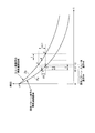
例えば、図3は、固定パターン表示部31Aとスルー画表示部31Bにおける輝度減衰曲線の例を示す図である。図3においては、横軸に時間t(表示時間t)を示し、縦軸に輝度Lを示してある。図3は、一定の条件下(例えば、発光素子に印加する駆動電圧(或いは駆動電流)が一定の条件下)における画素の表示時間tに対する輝度の時間変化特性を示したものである。
輝度減衰曲線Faは、固定パターン表示時(フル発光時)の輝度の減衰特性を示し、輝度減衰曲線Fbは、スルー画や静止画等の通常画像表示時の輝度の減衰特性を示している。
なお、輝度減衰曲線Fa及びFbの情報は、メモリ15に予め記憶されている。また、表示時間tは、信号処理用ASIC20内の表示時間計測部23により計測される。 For example, FIG. 3 is a diagram illustrating an example of a luminance attenuation curve in the fixedpattern display unit 31A and the through image display unit 31B. In FIG. 3, the horizontal axis indicates time t (display time t), and the vertical axis indicates luminance L. FIG. 3 shows the time variation characteristic of the luminance with respect to the display time t of the pixel under a certain condition (for example, a condition where the driving voltage (or driving current) applied to the light emitting element is constant).
The luminance attenuation curve Fa indicates the luminance attenuation characteristic when a fixed pattern is displayed (full light emission), and the luminance attenuation curve Fb indicates the luminance attenuation characteristic when a normal image such as a through image or a still image is displayed.
Information on the luminance decay curves Fa and Fb is stored in thememory 15 in advance. The display time t is measured by the display time measuring unit 23 in the signal processing ASIC 20.
輝度減衰曲線Faは、固定パターン表示時(フル発光時)の輝度の減衰特性を示し、輝度減衰曲線Fbは、スルー画や静止画等の通常画像表示時の輝度の減衰特性を示している。
なお、輝度減衰曲線Fa及びFbの情報は、メモリ15に予め記憶されている。また、表示時間tは、信号処理用ASIC20内の表示時間計測部23により計測される。 For example, FIG. 3 is a diagram illustrating an example of a luminance attenuation curve in the fixed
The luminance attenuation curve Fa indicates the luminance attenuation characteristic when a fixed pattern is displayed (full light emission), and the luminance attenuation curve Fb indicates the luminance attenuation characteristic when a normal image such as a through image or a still image is displayed.
Information on the luminance decay curves Fa and Fb is stored in the
図3の輝度減衰曲線FaおよびFbに示すように、固定パターンを表示させた場合(輝度減衰曲線Faの場合)と、スルー画を表示させた場合(輝度減衰曲線Fbの場合)では、一定の時間t1の経過後には、固定パターン表示部31Aと、スルー画表示部31Bとの間には、ΔLの輝度差が発生する。
As shown in the luminance attenuation curves Fa and Fb in FIG. 3, the fixed pattern is displayed (in the case of the luminance attenuation curve Fa) and the through image is displayed (in the case of the luminance attenuation curve Fb). After the elapse of time t1, a luminance difference of ΔL occurs between the fixed pattern display unit 31A and the through image display unit 31B.
この場合、固定パターン表示部31Aにおける表示時間t1を計測することにより、点a及び点bにおける輝度が分かるので、点bにおける輝度を、点aに示す輝度に補正(点bの輝度をΔLだけ低下)することにより、スルー画表示部31Bにおける輝度を固定パターン表示部31Aと同じ輝度にすることができる。
これにより、固定パターン表示部31Aとスルー画表示部31Bとの間の輝度のバラツキを補正することができる。 In this case, by measuring the display time t1 in the fixedpattern display portion 31A, the luminance at the point a and the point b can be known, so the luminance at the point b is corrected to the luminance indicated by the point a (the luminance at the point b is set to ΔL). The brightness of the through image display unit 31B can be made the same as that of the fixed pattern display unit 31A.
Thereby, the variation in luminance between the fixedpattern display unit 31A and the through image display unit 31B can be corrected.
これにより、固定パターン表示部31Aとスルー画表示部31Bとの間の輝度のバラツキを補正することができる。 In this case, by measuring the display time t1 in the fixed
Thereby, the variation in luminance between the fixed
なお、スルー画表示部31Bの輝度を減少させて固定パターン表示部31Aの輝度とスルー画表示部31Bの輝度とを合わせる方法の他に、逆に、固定パターン表示部31Aの輝度を上昇させて固定パターン表示部31Aの輝度とスルー画表示部31Bの輝度とを合わせる方法もある。
なお、スルー画表示部31Bの輝度を減少させて固定パターン表示部31Aの輝度とスルー画表示部31Bの輝度とを合わせる方法を用いることで、消費電力の低減を図るとともにEVF31の寿命が短くなることを避けることができる。
代替的には、スルー画表示部31Bにおける輝度を所定の割合で低下させ、同時に固定パターン表示部31Aの輝度を所定の割合で増加させることにより、固定パターン表示部31Aの輝度とスルー画表示部31Bの輝度とを合わせることも可能である。 In addition to decreasing the brightness of the liveview display unit 31B and matching the brightness of the fixed pattern display unit 31A with the brightness of the live view display unit 31B, conversely, increasing the brightness of the fixed pattern display unit 31A. There is also a method of matching the luminance of the fixed pattern display unit 31A with the luminance of the through image display unit 31B.
In addition, by reducing the luminance of the throughimage display unit 31B and using the method of matching the luminance of the fixed pattern display unit 31A and the luminance of the through image display unit 31B, the power consumption is reduced and the life of the EVF 31 is shortened. You can avoid that.
Alternatively, the luminance of the fixedpattern display unit 31A and the through image display unit are reduced by decreasing the luminance in the through image display unit 31B at a predetermined rate and simultaneously increasing the luminance of the fixed pattern display unit 31A at a predetermined rate. It is also possible to match the luminance of 31B.
なお、スルー画表示部31Bの輝度を減少させて固定パターン表示部31Aの輝度とスルー画表示部31Bの輝度とを合わせる方法を用いることで、消費電力の低減を図るとともにEVF31の寿命が短くなることを避けることができる。
代替的には、スルー画表示部31Bにおける輝度を所定の割合で低下させ、同時に固定パターン表示部31Aの輝度を所定の割合で増加させることにより、固定パターン表示部31Aの輝度とスルー画表示部31Bの輝度とを合わせることも可能である。 In addition to decreasing the brightness of the live
In addition, by reducing the luminance of the through
Alternatively, the luminance of the fixed
また、図3に示す輝度減衰曲線Faと輝度減衰曲線Fbとは、表示時間と減衰量(或いは補正量ΔL)とを対応付けしたテーブルの形式でメモリ15に記憶することができる。
また、輝度減衰曲線Fa及びFbを、表示時間tを変数とする関数の形式で表現し、この関数を用いて、表示時間に対する減衰量(或いは補正量ΔL)を算出するようにしてもよい。 Further, the luminance attenuation curve Fa and the luminance attenuation curve Fb shown in FIG. 3 can be stored in thememory 15 in the form of a table in which the display time and the attenuation amount (or the correction amount ΔL) are associated with each other.
Further, the luminance attenuation curves Fa and Fb may be expressed in the form of a function having the display time t as a variable, and the attenuation amount (or correction amount ΔL) with respect to the display time may be calculated using this function.
また、輝度減衰曲線Fa及びFbを、表示時間tを変数とする関数の形式で表現し、この関数を用いて、表示時間に対する減衰量(或いは補正量ΔL)を算出するようにしてもよい。 Further, the luminance attenuation curve Fa and the luminance attenuation curve Fb shown in FIG. 3 can be stored in the
Further, the luminance attenuation curves Fa and Fb may be expressed in the form of a function having the display time t as a variable, and the attenuation amount (or correction amount ΔL) with respect to the display time may be calculated using this function.
図4は、焼き付き補正の動作を説明するための図である。図4は、横方向に時間tの経過を示し、縦方向に、焼き付き補正に使用する補正パルス信号と、EVF31上の各画素を順次に走査して発光駆動するためのピクセルクロック(PixCLK)と、ビデオ信号と、を並べて示したものである。
なお、図4に示す各信号は、コントローラIC30が信号処理用ASIC20から入力する信号である。コントローラIC30では、信号処理用ASIC20から入力したこれらの信号に基づいて、EVF31を発光駆動するための制御信号Ec、映像信号Ev、および制御電圧信号Evcを生成する。 FIG. 4 is a diagram for explaining the burn-in correction operation. FIG. 4 shows the elapse of time t in the horizontal direction, a correction pulse signal used for burn-in correction in the vertical direction, and a pixel clock (PixCLK) for sequentially driving each pixel on theEVF 31 to drive light emission. , Video signals are shown side by side.
Each signal shown in FIG. 4 is a signal that thecontroller IC 30 inputs from the signal processing ASIC 20. The controller IC 30 generates a control signal Ec, a video signal Ev, and a control voltage signal Evc for driving the EVF 31 to emit light based on these signals input from the signal processing ASIC 20.
なお、図4に示す各信号は、コントローラIC30が信号処理用ASIC20から入力する信号である。コントローラIC30では、信号処理用ASIC20から入力したこれらの信号に基づいて、EVF31を発光駆動するための制御信号Ec、映像信号Ev、および制御電圧信号Evcを生成する。 FIG. 4 is a diagram for explaining the burn-in correction operation. FIG. 4 shows the elapse of time t in the horizontal direction, a correction pulse signal used for burn-in correction in the vertical direction, and a pixel clock (PixCLK) for sequentially driving each pixel on the
Each signal shown in FIG. 4 is a signal that the
図4に示すように、コントローラIC30は、補正パルス信号がH状態の時には、固定パターン表示部31Aの画素として、L状態のときは、スルー画表示部31Bの画素として判別する。
そして、コントローラIC30では、表示時間計測部23から入力した時間データCt(固定パターン表示部31Aおよびスルー画表示部31Bにおける表示時間)と、メモリ15に記憶された輝度減衰曲線FaおよびFbのデータと、補正パルス信号とに基づいて、EVF31上のスルー画表示部31Bの画素の輝度の調整を行う。 As shown in FIG. 4, thecontroller IC 30 determines the pixel of the fixed pattern display unit 31A when the correction pulse signal is in the H state and the pixel of the through image display unit 31B when the correction pulse signal is in the L state.
In thecontroller IC 30, the time data Ct (display time in the fixed pattern display unit 31 A and the through image display unit 31 B) input from the display time measurement unit 23 and the data of the luminance attenuation curves Fa and Fb stored in the memory 15 are stored. Based on the correction pulse signal, the luminance of the pixel of the through image display unit 31B on the EVF 31 is adjusted.
そして、コントローラIC30では、表示時間計測部23から入力した時間データCt(固定パターン表示部31Aおよびスルー画表示部31Bにおける表示時間)と、メモリ15に記憶された輝度減衰曲線FaおよびFbのデータと、補正パルス信号とに基づいて、EVF31上のスルー画表示部31Bの画素の輝度の調整を行う。 As shown in FIG. 4, the
In the
より具体的には、コントローラIC30では、補正パルス信号がL状態のときは、図3において説明したように、スルー画表示部31Bにスルー画を表示するものとして、図3に示すΔLだけ輝度を下げることにより、固定パターン表示部31Aとの輝度差を補正する。
EVF31における輝度の調整は、コントローラIC30からEVF31に対して出力される制御電圧信号Evcにより行われる。制御電圧信号Evcにより、EVF31内の画素に印加する駆動電圧の大きさを制御(画素に流れる電流を制御)することにより、輝度の調整を行う。 More specifically, in thecontroller IC 30, when the correction pulse signal is in the L state, as described in FIG. 3, it is assumed that the through image is displayed on the through image display unit 31B, and the luminance is increased by ΔL shown in FIG. By lowering, the luminance difference from the fixed pattern display unit 31A is corrected.
The brightness adjustment in theEVF 31 is performed by the control voltage signal Evc output from the controller IC 30 to the EVF 31. The brightness is adjusted by controlling the magnitude of the drive voltage applied to the pixels in the EVF 31 (controlling the current flowing through the pixels) by the control voltage signal Evc.
EVF31における輝度の調整は、コントローラIC30からEVF31に対して出力される制御電圧信号Evcにより行われる。制御電圧信号Evcにより、EVF31内の画素に印加する駆動電圧の大きさを制御(画素に流れる電流を制御)することにより、輝度の調整を行う。 More specifically, in the
The brightness adjustment in the
なお、補正パルス信号について補足して説明すると、固定パターン表示部31Aに表示される画像は撮影情報等であることが多く、予めEVF31上での場所(画素のアドレス)は判明している。
そこで、信号処理用ASIC20は、コントローラIC30に出力するビデオ信号とピクセルクロック(PixCLK)に加えて、固定パターンの画素であることを示す補正パルス信号を生成してコントローラIC30に出力する。
コントローラIC30は、この補正パルス信号のH/L状態によって、輝度の補正を行う画素か行わない画素かを判別し、その判別結果に基づいて画素の輝度を調整する。 To supplement the correction pulse signal, the image displayed on the fixedpattern display unit 31A is often photographing information or the like, and the location (pixel address) on the EVF 31 is known in advance.
Therefore, thesignal processing ASIC 20 generates a correction pulse signal indicating that the pixel is a fixed pattern in addition to the video signal and the pixel clock (PixCLK) to be output to the controller IC 30 and outputs them to the controller IC 30.
Based on the H / L state of the correction pulse signal, thecontroller IC 30 determines whether the pixel is subjected to luminance correction or not, and adjusts the luminance of the pixel based on the determination result.
そこで、信号処理用ASIC20は、コントローラIC30に出力するビデオ信号とピクセルクロック(PixCLK)に加えて、固定パターンの画素であることを示す補正パルス信号を生成してコントローラIC30に出力する。
コントローラIC30は、この補正パルス信号のH/L状態によって、輝度の補正を行う画素か行わない画素かを判別し、その判別結果に基づいて画素の輝度を調整する。 To supplement the correction pulse signal, the image displayed on the fixed
Therefore, the
Based on the H / L state of the correction pulse signal, the
また、時間データCtについては、撮影情報等の固定パターンの表示の有無は、制御部13内で把握できているため、制御部13が表示時間計測部23を制御することにより、固定パターンが表示されている時間を表示時間計測部23によりカウントすることができる。
コントローラIC30は、固定パターンが表示されていた時間の計測結果と、スルー画の表示時間の計測結果とを、表示時間計測部23から時間データCtとして入力し、メモリ15に記憶された輝度減衰曲線FaおよびFbのデータを参照して、固定パターン表示部31Aとスルー画表示部31Bとにおける輝度差を算出する。 In addition, regarding the time data Ct, since the presence or absence of display of a fixed pattern such as shooting information can be grasped in thecontrol unit 13, the control unit 13 controls the display time measuring unit 23 to display the fixed pattern. The displayed time can be counted by the display time measuring unit 23.
Thecontroller IC 30 inputs the measurement result of the time during which the fixed pattern was displayed and the measurement result of the through image display time as time data Ct from the display time measurement unit 23, and the luminance attenuation curve stored in the memory 15. The brightness difference between the fixed pattern display unit 31A and the through image display unit 31B is calculated with reference to the data of Fa and Fb.
コントローラIC30は、固定パターンが表示されていた時間の計測結果と、スルー画の表示時間の計測結果とを、表示時間計測部23から時間データCtとして入力し、メモリ15に記憶された輝度減衰曲線FaおよびFbのデータを参照して、固定パターン表示部31Aとスルー画表示部31Bとにおける輝度差を算出する。 In addition, regarding the time data Ct, since the presence or absence of display of a fixed pattern such as shooting information can be grasped in the
The
図5は、固定パターン表示部31Aにスルー画も表示する場合の例を示す図である。固定パターン表示部31Aには、スルー画も表示することが普通である。例えば、全画面表示(固定パターン表示を消す表示状態)の場合は、固定パターン表示部31Aにスルー画が表示される。
固定パターン表示部31Aにスルー画を表示する場合は、画素における輝度の減衰はスルー画表示の輝度減衰曲線Fbに従って遷移することになる。 FIG. 5 is a diagram illustrating an example in which a through image is also displayed on the fixedpattern display unit 31A. Usually, a through image is also displayed on the fixed pattern display portion 31A. For example, in the case of full screen display (display state in which the fixed pattern display is erased), a through image is displayed on the fixed pattern display portion 31A.
When a through image is displayed on the fixedpattern display unit 31A, the luminance attenuation in the pixel changes according to the luminance attenuation curve Fb of the through image display.
固定パターン表示部31Aにスルー画を表示する場合は、画素における輝度の減衰はスルー画表示の輝度減衰曲線Fbに従って遷移することになる。 FIG. 5 is a diagram illustrating an example in which a through image is also displayed on the fixed
When a through image is displayed on the fixed
図5に示す例では、時刻0から時刻t0の期間において、固定パターン表示部31Aは、フル発光(固定パターン表示)で画像を表示し、輝度の減衰はフル発光時の輝度減衰曲線Faに従って遷移する。
そして、時刻t0から時刻t1の間は、固定パターン表示部31Aにおいて固定パターン(文字情報等)に替えてスルー画(或いは静止画)が表示される。このため、時刻t0から時刻t1の間は、固定パターン表示部31Aにおける輝度減衰曲線Faが、スルー画表示の輝度減衰曲線Fbに置き換わる。
この場合、スルー画表示の時間(T=t0-t1)における輝度の減衰(曲線Fb上の点a’と点b’間の輝度の減衰量ΔL)を、フル発光時の輝度の減衰量(輝度減衰曲線Fa上の点aと点b間の減衰量)へ置き換えるようにする。 In the example shown in FIG. 5, in the period fromtime 0 to time t0, the fixed pattern display unit 31A displays an image with full light emission (fixed pattern display), and the luminance attenuation transitions according to the luminance attenuation curve Fa during full light emission. To do.
Then, during time t0 to time t1, a through image (or still image) is displayed in place of the fixed pattern (character information or the like) on the fixedpattern display unit 31A. For this reason, between time t0 and time t1, the luminance attenuation curve Fa in the fixed pattern display unit 31A is replaced with the luminance attenuation curve Fb of the through image display.
In this case, the luminance attenuation (the luminance attenuation ΔL between the points a ′ and b ′ on the curve Fb) in the through image display time (T = t0−t1) is expressed as the luminance attenuation amount at the time of full light emission ( (Attenuation amount between point a and point b on the luminance attenuation curve Fa).
そして、時刻t0から時刻t1の間は、固定パターン表示部31Aにおいて固定パターン(文字情報等)に替えてスルー画(或いは静止画)が表示される。このため、時刻t0から時刻t1の間は、固定パターン表示部31Aにおける輝度減衰曲線Faが、スルー画表示の輝度減衰曲線Fbに置き換わる。
この場合、スルー画表示の時間(T=t0-t1)における輝度の減衰(曲線Fb上の点a’と点b’間の輝度の減衰量ΔL)を、フル発光時の輝度の減衰量(輝度減衰曲線Fa上の点aと点b間の減衰量)へ置き換えるようにする。 In the example shown in FIG. 5, in the period from
Then, during time t0 to time t1, a through image (or still image) is displayed in place of the fixed pattern (character information or the like) on the fixed
In this case, the luminance attenuation (the luminance attenuation ΔL between the points a ′ and b ′ on the curve Fb) in the through image display time (T = t0−t1) is expressed as the luminance attenuation amount at the time of full light emission ( (Attenuation amount between point a and point b on the luminance attenuation curve Fa).
より具体的には、第1の手順として、表示時間計測部23は、スルー画の表示を開始する時点(時刻t0)における輝度減衰曲線Faにおける輝度(点aの輝度)を基点となる第1の輝度とする。
そして、輝度減衰曲線Fbにおいて、スルー画の表示時間(T)に対応して、基点となる第1の輝度(点a’の輝度(=点aの輝度))からの輝度の減衰量(点a’から点b’までの輝度の減衰量ΔL)を算出する。 More specifically, as a first procedure, the display time measurement unit 23 uses the luminance (the luminance at the point a) in the luminance attenuation curve Fa at the time when the display of the through image is started (time t0) as the first point. Brightness.
Then, in the luminance attenuation curve Fb, corresponding to the through image display time (T), the luminance attenuation amount (point) from the first luminance (the luminance at the point a ′ (= the luminance at the point a)) as the base point The luminance attenuation amount ΔL) from a ′ to the point b ′ is calculated.
次に、第2手順として、上記第1の手順で算出した輝度減衰曲線Fbにおける輝度の減衰量(ΔL)を、輝度減衰曲線Faにおける第1の輝度(点aの輝度)からの減衰量と見なし、第2の輝度(点bの輝度(=点b’の輝度))を算出する。
このようにして、スルー画表示による輝度減衰曲線Fbにおける輝度の減衰量を、輝度減衰曲線Faにおける輝度の減衰量に置き換える。 Next, as a second procedure, the luminance attenuation amount (ΔL) in the luminance attenuation curve Fb calculated in the first procedure is set as the attenuation amount from the first luminance (the luminance at the point a) in the luminance attenuation curve Fa. The second luminance (the luminance at the point b (= the luminance at the point b ′)) is calculated.
In this way, the luminance attenuation amount in the luminance attenuation curve Fb by the through image display is replaced with the luminance attenuation amount in the luminance attenuation curve Fa.
そして、第3の手順として、固定パターン表示部31Aにおいてスルー画表示を終了した時点(時刻t1)において、輝度減衰曲線Faにおける第2の輝度(点bの輝度)に対応する表示時間t1’(=t0+Δt)を、固定パターン表示部31Aにおける固定パターンの表示時間とする。
このようにして、固定パターン表示部31Aにスルー画が表示される場合においても、このスルー画表示による輝度の減衰量(輝度減衰曲線Fb上の減衰量)を、固定パターン表示による輝度の減衰量(輝度減衰曲線Fa上の減衰量)に置き換えることができる。 Then, as a third procedure, when the through image display is finished in the fixedpattern display unit 31A (time t1), the display time t1 ′ (the brightness at the point b) corresponding to the second brightness (the brightness at the point b) in the brightness decay curve Fa is displayed. = T0 + Δt) is the fixed pattern display time in the fixed pattern display section 31A.
In this way, even when a through image is displayed on the fixedpattern display unit 31A, the luminance attenuation amount (attenuation amount on the luminance attenuation curve Fb) by this through image display is used as the luminance attenuation amount by the fixed pattern display. (Attenuation amount on the luminance attenuation curve Fa).
このようにして、固定パターン表示部31Aにスルー画が表示される場合においても、このスルー画表示による輝度の減衰量(輝度減衰曲線Fb上の減衰量)を、固定パターン表示による輝度の減衰量(輝度減衰曲線Fa上の減衰量)に置き換えることができる。 Then, as a third procedure, when the through image display is finished in the fixed
In this way, even when a through image is displayed on the fixed
これにより、時刻t1において固定パターン表示部31Aとスルー画表示部31Bとの輝度差ΔL1(点cと点b間の輝度差)を算出することができるので、この輝度差ΔL1を補正すればよい。
このようにして、固定パターン表示部31Aにスルー画を表示する場合においても、スルー画表示による輝度の減衰量を、固定パターン表示による輝度の減衰量に置き換えることができるので、輝度減衰曲線FaおよびFbと、表示時間t1およびt1’とを基にして、画像表示パネル上での輝度のバラツキを補正することができる。 As a result, the luminance difference ΔL1 (luminance difference between the points c and b) between the fixedpattern display unit 31A and the through image display unit 31B can be calculated at time t1, and the luminance difference ΔL1 may be corrected. .
In this way, even when a through image is displayed on the fixedpattern display unit 31A, the luminance attenuation amount by the through image display can be replaced with the luminance attenuation amount by the fixed pattern display. Based on Fb and the display times t1 and t1 ′, it is possible to correct the luminance variation on the image display panel.
このようにして、固定パターン表示部31Aにスルー画を表示する場合においても、スルー画表示による輝度の減衰量を、固定パターン表示による輝度の減衰量に置き換えることができるので、輝度減衰曲線FaおよびFbと、表示時間t1およびt1’とを基にして、画像表示パネル上での輝度のバラツキを補正することができる。 As a result, the luminance difference ΔL1 (luminance difference between the points c and b) between the fixed
In this way, even when a through image is displayed on the fixed
以上、本発明の実施形態として、電子カメラのEVF31を画像表示装置10により制御することにより、固定パターン表示部31Aの焼き付きによる輝度のバラツキを補正する例について説明したが、本発明の画像表示装置は、これに限定されない。
As described above, as an embodiment of the present invention, an example has been described in which the EVF 31 of the electronic camera is controlled by the image display device 10 to correct the luminance variation due to the burn-in of the fixed pattern display unit 31A. Is not limited to this.
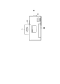
例えば、本発明の画像表示装置による焼き付き補正(輝度のバラツキの補正)を、図6に示す電子カメラ1Aの背面表示パネル32に対しても行うことができる。この背面表示パネル32は、通常は有機ELや液晶表示素子で構成されており、この背面表示パネル32に対しても焼き付き補正を行うことができる。
特に背面表示パネル32が有機EL素子である場合に、本発明による焼き付き補正を行うことにより、固定パターン表示部とスルー画表示部との間における輝度のバラツキを効果的に補正することができる。
なお、電子カメラ1Aの背面表示パネル32に対する焼き付き補正の制御方法は、図1から図5で説明したEVF31に対する焼き付き補正の制御方法と同様であり、重複する説明は省略する。 For example, the burn-in correction (correction of luminance variation) by the image display apparatus of the present invention can be performed on therear display panel 32 of the electronic camera 1A shown in FIG. The rear display panel 32 is usually composed of an organic EL or a liquid crystal display element, and the burn-in correction can be performed on the rear display panel 32 as well.
In particular, when therear display panel 32 is an organic EL element, by performing the burn-in correction according to the present invention, it is possible to effectively correct the luminance variation between the fixed pattern display unit and the through image display unit.
Note that the burn-in correction control method for therear display panel 32 of the electronic camera 1A is the same as the burn-in correction control method for the EVF 31 described with reference to FIGS.
特に背面表示パネル32が有機EL素子である場合に、本発明による焼き付き補正を行うことにより、固定パターン表示部とスルー画表示部との間における輝度のバラツキを効果的に補正することができる。
なお、電子カメラ1Aの背面表示パネル32に対する焼き付き補正の制御方法は、図1から図5で説明したEVF31に対する焼き付き補正の制御方法と同様であり、重複する説明は省略する。 For example, the burn-in correction (correction of luminance variation) by the image display apparatus of the present invention can be performed on the
In particular, when the
Note that the burn-in correction control method for the
さらに、本発明の画像表示装置は、固定パターンを表示する画像表示パネルを備えるすべての画像表示装置に適用できる。例えば、上述した電子カメラの他に、プロジェクタ等の電子機器や、携帯電話等の情報端末などの画素表示装置に適用できる。さらには、テレビの画像表示装置(例えば、メニューパターン画面を表示する表示装置)にも適用できる。
また、本発明は、有機ELを用いた画像表示パネルのみならず、液晶表示素子、プラズマディスプレイを用いた画像表示パネルを備える画像表示装置にも適用できる。 Furthermore, the image display device of the present invention can be applied to all image display devices including an image display panel that displays a fixed pattern. For example, in addition to the electronic camera described above, the present invention can be applied to electronic devices such as projectors and pixel display devices such as information terminals such as mobile phones. Furthermore, the present invention can be applied to a television image display device (for example, a display device that displays a menu pattern screen).
The present invention can be applied not only to an image display panel using an organic EL, but also to an image display device including an image display panel using a liquid crystal display element and a plasma display.
上述のように、本発明の画像表示装置は、プロジェクタなどの電子機器にも効果的に適用できる。図7Aは、有機ELや液晶の画像表示パネル41を用いたプロジェクタの例を示す図である。
プロジェクタ40は、画像表示パネル41と、光源42と、集光レンズ43と、ビームスプリッタ44と、投影レンズ45等を主要な構成要素とするプロジェクタである。このプロジェクタ40は、画像表示パネル41上に表示される画像を、光源42と、集光レンズ43と、ビームスプリッタ44と、投影レンズ45を用いてスクリーン46上に投影して映し出す装置である。
このプロジェクタ40に使用される画像表示パネル41を、本発明の画像表示装置を用いて制御することにより、画像表示パネル41上の固定パターン表示部における焼き付きにより発生する輝度のバラツキを補正することができる。 As described above, the image display device of the present invention can be effectively applied to electronic devices such as projectors. FIG. 7A is a diagram illustrating an example of a projector using an organic EL or liquid crystalimage display panel 41.
Theprojector 40 is a projector that includes an image display panel 41, a light source 42, a condenser lens 43, a beam splitter 44, a projection lens 45, and the like as main components. The projector 40 is a device that projects and displays an image displayed on the image display panel 41 on a screen 46 using a light source 42, a condenser lens 43, a beam splitter 44, and a projection lens 45.
By controlling theimage display panel 41 used in the projector 40 by using the image display device of the present invention, it is possible to correct variations in luminance caused by image sticking in the fixed pattern display unit on the image display panel 41. it can.
プロジェクタ40は、画像表示パネル41と、光源42と、集光レンズ43と、ビームスプリッタ44と、投影レンズ45等を主要な構成要素とするプロジェクタである。このプロジェクタ40は、画像表示パネル41上に表示される画像を、光源42と、集光レンズ43と、ビームスプリッタ44と、投影レンズ45を用いてスクリーン46上に投影して映し出す装置である。
このプロジェクタ40に使用される画像表示パネル41を、本発明の画像表示装置を用いて制御することにより、画像表示パネル41上の固定パターン表示部における焼き付きにより発生する輝度のバラツキを補正することができる。 As described above, the image display device of the present invention can be effectively applied to electronic devices such as projectors. FIG. 7A is a diagram illustrating an example of a projector using an organic EL or liquid crystal
The
By controlling the
図7Bは、プロジェクタを内蔵する電子カメラの例を示しており、本体側の電子カメラ1Bに、図7Aに示すプロジェクタ40をアクセサリとして内蔵させたものである。
図7Bに示すプロジェクタ内蔵カメラ50では、図6に示したカメラ側のEVF31及び背面表示パネル32に対して、本発明の画像表示装置を用いて焼き付き補正が行える他、図7Aに示したプロジェクタ40内の画像表示パネル41に対しても焼き付き補正を行うことができる。 FIG. 7B shows an example of an electronic camera with a built-in projector. Theprojector 40 shown in FIG. 7A is built in the electronic camera 1B on the main body side as an accessory.
In the camera with a built-inprojector 50 shown in FIG. 7B, the EVF 31 and the rear display panel 32 on the camera side shown in FIG. 6 can be corrected for burn-in using the image display device of the present invention, and the projector 40 shown in FIG. The burn-in correction can also be performed on the image display panel 41 in the inside.
図7Bに示すプロジェクタ内蔵カメラ50では、図6に示したカメラ側のEVF31及び背面表示パネル32に対して、本発明の画像表示装置を用いて焼き付き補正が行える他、図7Aに示したプロジェクタ40内の画像表示パネル41に対しても焼き付き補正を行うことができる。 FIG. 7B shows an example of an electronic camera with a built-in projector. The
In the camera with a built-in
また、本発明の画像表示装置による焼き付き補正は、携帯電話等の情報端末の画像表示パネルに適用できる。
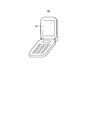
例えば、図8は、折り畳み式の携帯電話例であり、この情報端末(携帯電話)60の画像表示パネル61に対しても焼き付き補正を行うことができる。
また、本発明の画像表示装置による焼き付き補正は、携帯電話に限らず、PDA(Personal Digital Assistants)などの携帯情報端末の画像表示パネルにも適用できる。
さらに、本発明の画像表示装置による焼き付き補正は、タブレットPC等のパーソナルコンピュータ(PC)において、画像表示パネルに固定パターンを表示する場合にも、効果的に適用できる。
また、本発明の画像表示装置による焼き付き補正は、ブラウン管において固定パターンを表示する場合にも、効果的に適用できる。 The burn-in correction by the image display device of the present invention can be applied to an image display panel of an information terminal such as a mobile phone.
For example, FIG. 8 shows an example of a foldable mobile phone, and the burn-in correction can be performed on theimage display panel 61 of the information terminal (mobile phone) 60.
Further, the burn-in correction by the image display device of the present invention can be applied not only to a mobile phone but also to an image display panel of a portable information terminal such as a PDA (Personal Digital Assistant).
Further, the burn-in correction by the image display apparatus of the present invention can be effectively applied to a case where a fixed pattern is displayed on the image display panel in a personal computer (PC) such as a tablet PC.
Further, the burn-in correction by the image display apparatus of the present invention can be effectively applied even when a fixed pattern is displayed on a cathode ray tube.
例えば、図8は、折り畳み式の携帯電話例であり、この情報端末(携帯電話)60の画像表示パネル61に対しても焼き付き補正を行うことができる。
また、本発明の画像表示装置による焼き付き補正は、携帯電話に限らず、PDA(Personal Digital Assistants)などの携帯情報端末の画像表示パネルにも適用できる。
さらに、本発明の画像表示装置による焼き付き補正は、タブレットPC等のパーソナルコンピュータ(PC)において、画像表示パネルに固定パターンを表示する場合にも、効果的に適用できる。
また、本発明の画像表示装置による焼き付き補正は、ブラウン管において固定パターンを表示する場合にも、効果的に適用できる。 The burn-in correction by the image display device of the present invention can be applied to an image display panel of an information terminal such as a mobile phone.
For example, FIG. 8 shows an example of a foldable mobile phone, and the burn-in correction can be performed on the
Further, the burn-in correction by the image display device of the present invention can be applied not only to a mobile phone but also to an image display panel of a portable information terminal such as a PDA (Personal Digital Assistant).
Further, the burn-in correction by the image display apparatus of the present invention can be effectively applied to a case where a fixed pattern is displayed on the image display panel in a personal computer (PC) such as a tablet PC.
Further, the burn-in correction by the image display apparatus of the present invention can be effectively applied even when a fixed pattern is displayed on a cathode ray tube.
以上、本発明の実施形態について説明したが、ここで、本発明の態様と上記実施形態との対応関係について補足して説明しておく。
上記実施形態において、本発明の一態様における画像表示装置は、図1に示す電子カメラ1内の画像表示装置10(メモリ15と、表示時間計測部23と、コントローラIC30と、EVF31とで構成される部分)が対応し、本発明の一態様における表示時間計測部は、表示時間計測部23が対応し、本発明の一態様における記憶部は、メモリ15が対応し、本発明の一態様における輝度補正部は、コントローラIC30が対応する。
また、本発明の一態様における第1の表示領域は、図2に示す画像表示パネル(EVF31)上の固定パターン表示部31Aが対応し、本発明の一態様における第2の表示領域は、図2に示すスルー画表示部31Bが対応する。 The embodiment of the present invention has been described above. Here, the correspondence relationship between the aspect of the present invention and the above embodiment will be supplementarily described.
In the above-described embodiment, the image display device according to one aspect of the present invention includes the image display device 10 (thememory 15, the display time measurement unit 23, the controller IC 30, and the EVF 31 in the electronic camera 1 illustrated in FIG. The display time measurement unit in one embodiment of the present invention corresponds to the display time measurement unit 23, and the storage unit in one embodiment of the present invention corresponds to the memory 15 in one embodiment of the present invention. The controller IC 30 corresponds to the brightness correction unit.
The first display area in one embodiment of the present invention corresponds to the fixedpattern display portion 31A on the image display panel (EVF 31) illustrated in FIG. 2, and the second display area in one embodiment of the present invention is illustrated in FIG. 2 corresponds to a through image display unit 31B.
上記実施形態において、本発明の一態様における画像表示装置は、図1に示す電子カメラ1内の画像表示装置10(メモリ15と、表示時間計測部23と、コントローラIC30と、EVF31とで構成される部分)が対応し、本発明の一態様における表示時間計測部は、表示時間計測部23が対応し、本発明の一態様における記憶部は、メモリ15が対応し、本発明の一態様における輝度補正部は、コントローラIC30が対応する。
また、本発明の一態様における第1の表示領域は、図2に示す画像表示パネル(EVF31)上の固定パターン表示部31Aが対応し、本発明の一態様における第2の表示領域は、図2に示すスルー画表示部31Bが対応する。 The embodiment of the present invention has been described above. Here, the correspondence relationship between the aspect of the present invention and the above embodiment will be supplementarily described.
In the above-described embodiment, the image display device according to one aspect of the present invention includes the image display device 10 (the
The first display area in one embodiment of the present invention corresponds to the fixed
(1)そして、上記実施形態において、画像表示装置(画像表示装置10)は、所定の固定パターンを表示する第1の表示領域(固定パターン表示部31A)における画像表示時間と、第1の表示領域以外の第2の表示領域(スルー画表示部31B)における画像表示時間のそれぞれを計測する表示時間計測部23と、第1の表示領域と第2の表示領域とにおけるそれぞれの画像表示時間と、この画像表示時間に応じた輝度の補正量と、を対応付ける情報を記憶する記憶部(メモリ15)と、上記画像表示時間と輝度の補正量との情報に基づいて第1の表示領域(固定パターン表示部31A)および第2の表示領域(スルー画表示部31B)における表示画像の輝度の補正を行う輝度補正部(コントローラIC30)と、を備える。
(1) In the above-described embodiment, the image display device (image display device 10) displays the image display time in the first display area (fixed pattern display unit 31A) for displaying a predetermined fixed pattern, and the first display. A display time measuring unit 23 that measures each of the image display times in the second display region (through image display unit 31B) other than the region, and the respective image display times in the first display region and the second display region. A storage unit (memory 15) that stores information for associating the luminance correction amount according to the image display time, and the first display area (fixed) based on the information on the image display time and the luminance correction amount. A pattern display unit 31A) and a luminance correction unit (controller IC30) for correcting the luminance of the display image in the second display area (through image display unit 31B).
このような構成の画像表示装置(画像表示装置10)では、表示時間計測部23が、固定パターンを表示する第1の表示領域(固定パターン表示部31A)における表示時間と、第2の表示領域(スルー画表示部31B)における画像の表示時間とを、それぞれ計測する。
また、記憶部(メモリ15)には、第1の表示領域(固定パターン表示部31A)における固定パターンの画像表示時間と輝度の補正量とを対応付ける情報(第1の輝度減衰曲線Fa)と、第2の表示領域(スルー画表示部31B)におけるスルー画の画像表示時間と輝度の補正量とを対応づける情報(第2の輝度減衰曲線Fb)と、を記憶しておく。
そして、輝度補正部(コントローラIC30)は、第1の表示領域(固定パターン表示部31A)と第2の表示領域(スルー画表示部31B)におけるそれぞれの画像表示時間と、この画像表示時間と輝度の補正量(第1の輝度減衰曲線Fa及び第2の輝度減衰曲線Fb)の情報に基づいて、第1の表示領域(固定パターン表示部31A)および第2の表示領域(スルー画表示部31B)における表示画像の輝度の補正を行う。
これにより、画像表示パネル(EVF31)の固定パターンの表示領域(固定パターン表示部31A)における焼き付きにより発生する、画像表示パネル上での輝度のバラツキを補正することができる。 In the image display device (image display device 10) having such a configuration, the display time measurement unit 23 displays the display time in the first display region (fixedpattern display unit 31A) for displaying the fixed pattern, and the second display region. The display time of the image in the (through image display unit 31B) is measured.
Further, in the storage unit (memory 15), information (first luminance decay curve Fa) for associating the fixed pattern image display time and the luminance correction amount in the first display area (fixedpattern display unit 31A), and Information (second luminance attenuation curve Fb) that associates the image display time of the through image with the luminance correction amount in the second display area (through image display unit 31B) is stored.
The brightness correction unit (controller IC 30) then displays each image display time in the first display area (fixedpattern display part 31A) and the second display area (through image display part 31B), and the image display time and brightness. Based on the information of the correction amount (first luminance decay curve Fa and second luminance decay curve Fb), the first display area (fixed pattern display portion 31A) and the second display area (through image display portion 31B). The luminance of the display image is corrected in ().
Thereby, it is possible to correct the variation in luminance on the image display panel, which is caused by image sticking in the fixed pattern display area (fixedpattern display portion 31A) of the image display panel (EVF 31).
また、記憶部(メモリ15)には、第1の表示領域(固定パターン表示部31A)における固定パターンの画像表示時間と輝度の補正量とを対応付ける情報(第1の輝度減衰曲線Fa)と、第2の表示領域(スルー画表示部31B)におけるスルー画の画像表示時間と輝度の補正量とを対応づける情報(第2の輝度減衰曲線Fb)と、を記憶しておく。
そして、輝度補正部(コントローラIC30)は、第1の表示領域(固定パターン表示部31A)と第2の表示領域(スルー画表示部31B)におけるそれぞれの画像表示時間と、この画像表示時間と輝度の補正量(第1の輝度減衰曲線Fa及び第2の輝度減衰曲線Fb)の情報に基づいて、第1の表示領域(固定パターン表示部31A)および第2の表示領域(スルー画表示部31B)における表示画像の輝度の補正を行う。
これにより、画像表示パネル(EVF31)の固定パターンの表示領域(固定パターン表示部31A)における焼き付きにより発生する、画像表示パネル上での輝度のバラツキを補正することができる。 In the image display device (image display device 10) having such a configuration, the display time measurement unit 23 displays the display time in the first display region (fixed
Further, in the storage unit (memory 15), information (first luminance decay curve Fa) for associating the fixed pattern image display time and the luminance correction amount in the first display area (fixed
The brightness correction unit (controller IC 30) then displays each image display time in the first display area (fixed
Thereby, it is possible to correct the variation in luminance on the image display panel, which is caused by image sticking in the fixed pattern display area (fixed
(2)また、上記実施形態において、第1の表示領域(固定パターン表示部31A)と第2の表示領域(スルー画表示部31B)とにおける画像表示時間の計測と、この画像表示時間に応じた輝度の補正とが、第1の表示領域(固定パターン表示部31A)と第2の表示領域(スルー画表示部31B)とに含まれるそれぞれの画素ごとに行われる。
このような構成の画像表示装置(画像表示装置10)では、第1の表示領域(固定パターン表示部31A)と第2の表示領域(スルー画表示部31B)における輝度の補正を、画素ごとに行うようにしたので、画像表示パネル上での輝度のバラツキをきめ細かく補正することができる。 (2) In the above embodiment, the measurement of the image display time in the first display area (fixedpattern display section 31A) and the second display area (through image display section 31B), and the image display time. The correction of the brightness is performed for each pixel included in the first display area (fixed pattern display unit 31A) and the second display area (through image display unit 31B).
In the image display device (image display device 10) having such a configuration, luminance correction is performed for each pixel in the first display region (fixedpattern display unit 31A) and the second display region (through image display unit 31B). Since this is done, it is possible to finely correct variations in luminance on the image display panel.
このような構成の画像表示装置(画像表示装置10)では、第1の表示領域(固定パターン表示部31A)と第2の表示領域(スルー画表示部31B)における輝度の補正を、画素ごとに行うようにしたので、画像表示パネル上での輝度のバラツキをきめ細かく補正することができる。 (2) In the above embodiment, the measurement of the image display time in the first display area (fixed
In the image display device (image display device 10) having such a configuration, luminance correction is performed for each pixel in the first display region (fixed
(3)また、上記実施形態において、輝度補正部(コントローラIC30)は、第1の表示領域(固定パターン表示部31A)と第2の表示領域(スルー画表示部31B)とのいずれか一方、または両方の輝度を変更することにより、第1の表示領域(固定パターン表示部31A)と第2の表示領域(スルー画表示部31B)との間における輝度の差を補正する。
これにより、第1の表示領域(固定パターン表示部31A)と第2の表示領域(スルー画表示部31B)のいずれか一方、または両方の輝度を変更することにより、画像表示パネル上での輝度のバラツキを補正することができる。 (3) In the above embodiment, the luminance correction unit (controller IC 30) is either the first display region (fixedpattern display unit 31A) or the second display region (through image display unit 31B). Alternatively, the luminance difference between the first display area (fixed pattern display unit 31A) and the second display area (through image display unit 31B) is corrected by changing both luminances.
Accordingly, the luminance on the image display panel is changed by changing the luminance of one or both of the first display region (fixedpattern display unit 31A) and the second display region (through image display unit 31B). Can be corrected.
これにより、第1の表示領域(固定パターン表示部31A)と第2の表示領域(スルー画表示部31B)のいずれか一方、または両方の輝度を変更することにより、画像表示パネル上での輝度のバラツキを補正することができる。 (3) In the above embodiment, the luminance correction unit (controller IC 30) is either the first display region (fixed
Accordingly, the luminance on the image display panel is changed by changing the luminance of one or both of the first display region (fixed
(4)また、上記実施形態において、輝度補正部(コントローラIC30)は、第2の表示領域(スルー画表示部31B)の輝度を低減させることにより、第1の表示領域(固定パターン表示部31A)と第2の表示領域(スルー画表示部31B)との間における輝度の差を補正する。
これにより、消費電力の低減を図るとともに画像表示パネルの寿命が短くなることを回避しながら、画像表示パネル上での輝度のバラツキを補正することができる。 (4) In the above embodiment, the luminance correction unit (controller IC 30) reduces the luminance of the second display region (throughimage display unit 31B), thereby reducing the first display region (fixed pattern display unit 31A). ) And the second display area (through image display unit 31B) is corrected.
As a result, it is possible to correct variations in luminance on the image display panel while reducing power consumption and avoiding shortening the life of the image display panel.
これにより、消費電力の低減を図るとともに画像表示パネルの寿命が短くなることを回避しながら、画像表示パネル上での輝度のバラツキを補正することができる。 (4) In the above embodiment, the luminance correction unit (controller IC 30) reduces the luminance of the second display region (through
As a result, it is possible to correct variations in luminance on the image display panel while reducing power consumption and avoiding shortening the life of the image display panel.
(5)また、上記実施形態において、輝度補正部(コントローラIC30)は、第1の表示領域(固定パターン表示部31A)の輝度を増加させることにより、第1の表示領域(固定パターン表示部31A)と第2の表示領域(スルー画表示部31B)との間における輝度の差を補正する。
これにより、所望の場合には、第1の表示領域(固定パターン表示部31A)の輝度を増加させることにより、第1の表示領域(固定パターン表示部31A)と第2の表示領域(スルー画表示部31B)との間における輝度の差を補正することができる。 (5) In the above embodiment, the luminance correction unit (controller IC 30) increases the luminance of the first display region (fixedpattern display unit 31A), thereby increasing the first display region (fixed pattern display unit 31A). ) And the second display area (through image display unit 31B) is corrected.
Thus, if desired, the luminance of the first display area (fixedpattern display portion 31A) is increased to increase the first display area (fixed pattern display portion 31A) and the second display area (through image). The difference in luminance with respect to the display unit 31B) can be corrected.
これにより、所望の場合には、第1の表示領域(固定パターン表示部31A)の輝度を増加させることにより、第1の表示領域(固定パターン表示部31A)と第2の表示領域(スルー画表示部31B)との間における輝度の差を補正することができる。 (5) In the above embodiment, the luminance correction unit (controller IC 30) increases the luminance of the first display region (fixed
Thus, if desired, the luminance of the first display area (fixed
(6)また、上記実施形態において、上記輝度の補正が、第1の表示領域(固定パターン表示部31A)または第2の表示領域(スルー画表示部31B)内の画素の駆動電圧を調整することにより行われる。
これにより、画像表示パネルの画素の駆動電圧を調整して、画素の発光輝度をきめ細かくかつ容易に調整することができる。 (6) In the above embodiment, the luminance correction adjusts the driving voltage of the pixels in the first display area (fixedpattern display unit 31A) or the second display area (through image display unit 31B). Is done.
Thereby, the drive voltage of the pixel of the image display panel can be adjusted, and the light emission luminance of the pixel can be finely and easily adjusted.
これにより、画像表示パネルの画素の駆動電圧を調整して、画素の発光輝度をきめ細かくかつ容易に調整することができる。 (6) In the above embodiment, the luminance correction adjusts the driving voltage of the pixels in the first display area (fixed
Thereby, the drive voltage of the pixel of the image display panel can be adjusted, and the light emission luminance of the pixel can be finely and easily adjusted.
(7)また、上記実施形態において、記憶部(メモリ15)には、第1の表示領域(固定パターン表示部31A)における固定パターンの表示時間に対する画素の発光輝度の減衰特性を示す第1の輝度減衰曲線Fa(輝度減衰曲線Fa)の情報と、第2の表示領域(スルー画表示部31B)における固定パターン以外の画像の表示時間に対する画素の発光輝度の減衰特性を示す第2の輝度減衰曲線Fb(輝度減衰曲線Fb)の情報と、が記憶され、輝度補正部(コントローラIC30)は、第1の表示領域における固定パターンの表示時間と第2の表示領域における画像の表示時間とを基に、第1の輝度減衰曲線Faと第2の輝度減衰曲線Fbを参照して、第1の表示領域と第2の表示領域における画素の輝度差を算出する。
(7) Further, in the above embodiment, the storage unit (memory 15) has the first emission luminance attenuation characteristic of the pixel with respect to the fixed pattern display time in the first display area (fixed pattern display unit 31A). Second luminance attenuation indicating information on the luminance attenuation curve Fa (luminance attenuation curve Fa) and the emission luminance attenuation characteristic of the pixel with respect to the display time of an image other than the fixed pattern in the second display area (through image display unit 31B). The curve Fb (luminance decay curve Fb) information is stored, and the luminance correction unit (controller IC 30) is based on the fixed pattern display time in the first display area and the image display time in the second display area. In addition, the luminance difference between the pixels in the first display area and the second display area is calculated with reference to the first luminance attenuation curve Fa and the second luminance attenuation curve Fb.
このような構成の画像表示装置(画像表示装置10)では、記憶部(メモリ15)に、図3に示す固定パターンを表示する場合の発光輝度の減衰特性を示す第1の輝度減衰曲線Faと、固定パターン以外の画像を表示する場合の画素の発光輝度の減衰特性を示す第2の輝度減衰曲線Fbとを記憶する。
輝度補正部(コントローラIC30)は、第1の表示領域(固定パターン表示部31A)における固定パターンの表示時間と第2の表示領域(スルー画表示部31B)における画像(例えば、スルー画)の表示時間とを基に、第1の輝度減衰曲線Faと第2の輝度減衰曲線Fbを参照し、第1の表示領域(固定パターン表示部31A)と第2の表示領域(スルー画表示部31B)における画素の輝度差を算出する。
これにより、固定パターン表示部31Aとスルー画表示部31Bとにおける画像の表示時間を基に、輝度減衰曲線FaおよびFbを参照することにより、第1の表示領域(固定パターン表示部31A)と第2の表示領域(スルー画表示部31B)との間における輝度の差を算出することができる。 In the image display device (image display device 10) having such a configuration, the first luminance attenuation curve Fa indicating the emission luminance attenuation characteristic when the fixed pattern shown in FIG. The second luminance attenuation curve Fb indicating the attenuation characteristic of the emission luminance of the pixel when displaying an image other than the fixed pattern is stored.
The brightness correction unit (controller IC 30) displays the fixed pattern display time in the first display area (fixedpattern display unit 31A) and the image (for example, a through image) in the second display area (through image display unit 31B). Based on the time, the first display area (fixed pattern display unit 31A) and the second display area (through image display unit 31B) are referred to by referring to the first brightness decay curve Fa and the second brightness decay curve Fb. The luminance difference of the pixel at is calculated.
Thus, the first display area (fixedpattern display unit 31A) and the first display area are referred to by referring to the luminance attenuation curves Fa and Fb based on the display time of the images in the fixed pattern display unit 31A and the through image display unit 31B. It is possible to calculate the luminance difference between the two display areas (through image display unit 31B).
輝度補正部(コントローラIC30)は、第1の表示領域(固定パターン表示部31A)における固定パターンの表示時間と第2の表示領域(スルー画表示部31B)における画像(例えば、スルー画)の表示時間とを基に、第1の輝度減衰曲線Faと第2の輝度減衰曲線Fbを参照し、第1の表示領域(固定パターン表示部31A)と第2の表示領域(スルー画表示部31B)における画素の輝度差を算出する。
これにより、固定パターン表示部31Aとスルー画表示部31Bとにおける画像の表示時間を基に、輝度減衰曲線FaおよびFbを参照することにより、第1の表示領域(固定パターン表示部31A)と第2の表示領域(スルー画表示部31B)との間における輝度の差を算出することができる。 In the image display device (image display device 10) having such a configuration, the first luminance attenuation curve Fa indicating the emission luminance attenuation characteristic when the fixed pattern shown in FIG. The second luminance attenuation curve Fb indicating the attenuation characteristic of the emission luminance of the pixel when displaying an image other than the fixed pattern is stored.
The brightness correction unit (controller IC 30) displays the fixed pattern display time in the first display area (fixed
Thus, the first display area (fixed
(8)また、上記実施形態において、第1の表示領域(固定パターン表示部31A)において固定パターンに替えてスルー画が表示される場合は、表示時間計測部23により、スルー画の表示を開始する時点の第1の輝度減衰曲線Faにおける輝度を基点となる第1の輝度とし、第2の輝度減衰曲線において第1の輝度を基点として、スルー画の表示時間の間に第1の輝度から減衰する輝度の減衰量を算出する第1の手順と、第1の手順で算出した第2の輝度減衰曲線Fbにおける輝度の減衰量を第1の輝度減衰曲線Faにおける輝度の減衰量と見なし、第1の輝度減衰曲線Faにおける第2の輝度を算出することにより、スルー画表示による輝度の減衰量を第1の輝度減衰曲線Faにおける輝度の減衰量に置き換える第2の手順と、スルー画の表示を終了した時点において、第1の輝度減衰曲線Faにおける第2の輝度に対応する表示時間を、第1の表示領域(固定パターン表示部31A)における固定パターンの表示時間とする第3の手順と、が行われる。
(8) In the above embodiment, when a through image is displayed instead of the fixed pattern in the first display area (fixed pattern display unit 31A), the display time measurement unit 23 starts displaying the through image. The first luminance decay curve Fa at the time of the first luminance is set as the first luminance as the base point, and the first luminance is set as the base point in the second luminance decay curve from the first luminance during the display time of the through image. The first procedure for calculating the attenuation amount of the luminance to be attenuated and the luminance attenuation amount in the second luminance attenuation curve Fb calculated in the first procedure are regarded as the luminance attenuation amount in the first luminance attenuation curve Fa. By calculating the second luminance in the first luminance attenuation curve Fa, a second procedure for replacing the luminance attenuation amount by the live view display with the luminance attenuation amount in the first luminance attenuation curve Fa, When the display of the image is finished, the display time corresponding to the second luminance in the first luminance decay curve Fa is set as the fixed pattern display time in the first display area (fixed pattern display unit 31A). And the procedure is performed.
これにより、第1の表示領域(固定パターン表示部31A)にスルー画が表示される場合においても、このスルー画表示による輝度の減衰量(輝度減衰曲線Fb上での減衰)を、固定パターン表示による輝度の減衰量(輝度減衰曲線Fa上での減衰)に置き換えることができる。
Thus, even when a through image is displayed in the first display area (fixed pattern display portion 31A), the luminance attenuation amount (attenuation on the luminance attenuation curve Fb) by this through image display is displayed in the fixed pattern display. Can be replaced with the amount of luminance attenuation (attenuation on the luminance attenuation curve Fa).
(9)また、上記実施形態において、輝度の補正は、第2の表示領域(スルー画表示部31B)においてスルー画を表示する際に行われる。
これにより、第2の表示領域(スルー画表示部31B)にスルー画を表示する際に、第2の表示領域に表示される画像の輝度を、第1の表示領域(固定パターン表示部31A)に表示される画像の輝度に合わせることができる。 (9) In the above embodiment, the luminance correction is performed when a through image is displayed in the second display area (throughimage display unit 31B).
Thereby, when displaying a through image in the second display area (throughimage display unit 31B), the luminance of the image displayed in the second display area is set to the first display area (fixed pattern display unit 31A). Can be adjusted to the brightness of the image displayed on the screen.
これにより、第2の表示領域(スルー画表示部31B)にスルー画を表示する際に、第2の表示領域に表示される画像の輝度を、第1の表示領域(固定パターン表示部31A)に表示される画像の輝度に合わせることができる。 (9) In the above embodiment, the luminance correction is performed when a through image is displayed in the second display area (through
Thereby, when displaying a through image in the second display area (through
(10)また、上記実施形態において、画像表示装置(画像表示装置10)は、有機ELを画像表示パネルとして用いる。
これにより、有機ELを画像表示パネルに用いた画像表示装置において、画像表示パネルの固定パターンの表示領域における焼き付きにより発生する、画像表示パネル上での輝度のバラツキを補正することができる。 (10) In the above embodiment, the image display device (image display device 10) uses an organic EL as an image display panel.
Thereby, in the image display device using the organic EL for the image display panel, it is possible to correct the variation in luminance on the image display panel, which is caused by image sticking in the display area of the fixed pattern of the image display panel.
(11)また、上記実施形態において、電子機器は、上記のいずれかに記載の画像表示装置(画像表示装置10)を備える。
例えば、図7Aに示す電子機器(プロジェクタ40)において、画像表示パネル41を本発明の画像表示装置で駆動制御することにより、画像表示パネル41の固定パターンの表示領域における焼き付きにより発生する、画像表示パネル41上での輝度のバラツキを補正することができる。 (11) Moreover, in the said embodiment, an electronic device is provided with the image display apparatus (image display apparatus 10) in any one of said.
For example, in the electronic device (projector 40) shown in FIG. 7A, theimage display panel 41 is driven and controlled by the image display device of the present invention, thereby causing image display caused by burn-in in the fixed pattern display area of the image display panel 41. The luminance variation on the panel 41 can be corrected.
例えば、図7Aに示す電子機器(プロジェクタ40)において、画像表示パネル41を本発明の画像表示装置で駆動制御することにより、画像表示パネル41の固定パターンの表示領域における焼き付きにより発生する、画像表示パネル41上での輝度のバラツキを補正することができる。 (11) Moreover, in the said embodiment, an electronic device is provided with the image display apparatus (image display apparatus 10) in any one of said.
For example, in the electronic device (projector 40) shown in FIG. 7A, the
(12)上記実施形態において、電子カメラは、上記のいずれかに記載の画像表示装置(画像表示装置10)を備える。
例えば、図6に示す電子カメラ1Aにおいて、EVF31および背面表示パネル32を本発明の画像表示装置(画像表示装置10)で駆動制御することにより、電子カメラ1AのEVF31および背面表示パネル32において、固定パターンの表示領域における焼き付きにより発生する輝度のバラツキを補正することができる。 (12) In the above-described embodiment, the electronic camera includes the image display device (image display device 10) described above.
For example, in theelectronic camera 1A shown in FIG. 6, the EVF 31 and the rear display panel 32 are driven and controlled by the image display device (image display device 10) of the present invention, so that the EVF 31 and the rear display panel 32 of the electronic camera 1A are fixed. It is possible to correct luminance variations caused by burn-in in the pattern display area.
例えば、図6に示す電子カメラ1Aにおいて、EVF31および背面表示パネル32を本発明の画像表示装置(画像表示装置10)で駆動制御することにより、電子カメラ1AのEVF31および背面表示パネル32において、固定パターンの表示領域における焼き付きにより発生する輝度のバラツキを補正することができる。 (12) In the above-described embodiment, the electronic camera includes the image display device (image display device 10) described above.
For example, in the
(13)上記実施形態において、情報端末は、上記のいずれかに記載の画像表示装置(画像表示装置10)を備える。
例えば、図8に示す携帯電話等の情報端末60において、画像表示パネル61を本発明の画像表示装置で駆動制御することにより、画像表示パネル61において、固定パターンの表示領域における焼き付きにより発生する輝度のバラツキを補正することができる。 (13) In the above embodiment, an information terminal includes the image display device (image display device 10) described above.
For example, in theinformation terminal 60 such as a mobile phone shown in FIG. 8, the image display panel 61 is driven and controlled by the image display device of the present invention, so that the luminance generated by the burn-in in the fixed pattern display area in the image display panel 61. Can be corrected.
例えば、図8に示す携帯電話等の情報端末60において、画像表示パネル61を本発明の画像表示装置で駆動制御することにより、画像表示パネル61において、固定パターンの表示領域における焼き付きにより発生する輝度のバラツキを補正することができる。 (13) In the above embodiment, an information terminal includes the image display device (image display device 10) described above.
For example, in the
以上、本発明の実施の形態について説明したが、本発明の画像表示装置は、上述の図示例にのみ限定されるものではなく、本発明の要旨を逸脱しない範囲内において種々変更を加え得ることは勿論である。
Although the embodiment of the present invention has been described above, the image display apparatus of the present invention is not limited to the above illustrated example, and various modifications can be made without departing from the gist of the present invention. Of course.
1,1A,1B…電子カメラ、10…画像表示装置、11…撮影レンズ、12…撮像素子、13…制御部、14…記録部、15…メモリ、20…信号処理用ASIC、21…前処理部、22…信号処理部、23…表示時間計測部、24…撮影情報表示変更部、30…コントローラIC、31…EVF、31A…固定パターン表示部、31B…スルー画表示部、32…背面表示パネル、40…プロジェクタ、41…画像表示パネル、50…プロジェクタ内蔵カメラ、60…情報端末、61…画像表示パネル。
DESCRIPTION OF SYMBOLS 1,1A, 1B ... Electronic camera, 10 ... Image display apparatus, 11 ... Shooting lens, 12 ... Image sensor, 13 ... Control part, 14 ... Recording part, 15 ... Memory, 20 ... Signal processing ASIC, 21 ... Pre-processing , 22 ... Signal processing unit, 23 ... Display time measurement unit, 24 ... Shooting information display change unit, 30 ... Controller IC, 31 ... EVF, 31A ... Fixed pattern display unit, 31B ... Through image display unit, 32 ... Back display Panel, 40 ... projector, 41 ... image display panel, 50 ... camera with built-in projector, 60 ... information terminal, 61 ... image display panel.
Claims (13)
- 所定の固定パターンを表示する第1の表示領域における画像表示時間と、前記第1の表示領域以外の第2の表示領域における画像表示時間のそれぞれを計測する表示時間計測部と、
前記第1の表示領域と前記第2の表示領域とにおけるそれぞれの画像表示時間と、前記画像表示時間に応じた輝度の補正量と、を対応付ける情報を記憶する記憶部と、
前記画像表示時間と前記輝度の補正量との情報に基づいて前記第1の表示領域および前記第2の表示領域における表示画像の輝度の補正を行う輝度補正部と、
を備えることを特徴とする画像表示装置。 A display time measuring unit for measuring each of an image display time in a first display area for displaying a predetermined fixed pattern and an image display time in a second display area other than the first display area;
A storage unit for storing information associating each image display time in the first display region and the second display region with a luminance correction amount corresponding to the image display time;
A luminance correction unit that corrects the luminance of the display image in the first display area and the second display area based on information on the image display time and the luminance correction amount;
An image display device comprising: - 前記第1の表示領域と前記第2の表示領域とにおける画像表示時間の計測と、前記画像表示時間に応じた輝度の補正とが、前記第1の表示領域と前記第2の表示領域とに含まれるそれぞれの画素ごとに行われる
ことを特徴とする請求項1に記載の画像表示装置。 The measurement of the image display time in the first display area and the second display area and the correction of the luminance according to the image display time are performed in the first display area and the second display area. The image display device according to claim 1, wherein the image display device is performed for each pixel included. - 前記輝度補正部は、前記第1の表示領域と前記第2の表示領域とのいずれか一方、または両方の輝度を変更することにより、前記第1の表示領域と前記第2の表示領域との間における輝度の差を補正する
ことを特徴とする請求項1または請求項2に記載の画像表示装置。 The brightness correction unit changes the brightness of one or both of the first display area and the second display area, thereby changing the brightness between the first display area and the second display area. The image display device according to claim 1, wherein a difference in brightness between the images is corrected. - 前記輝度補正部は、前記第2の表示領域の輝度を低減させることにより、前記第1の表示領域と前記第2の表示領域との間における輝度の差を補正する
ことを特徴とする請求項1または請求項2に記載の画像表示装置。 The brightness correction unit corrects a brightness difference between the first display area and the second display area by reducing the brightness of the second display area. The image display device according to claim 1 or 2. - 前記輝度補正部は、前記第1の表示領域の輝度を増加させることにより、前記第1の表示領域と前記第2の表示領域との間における輝度の差を補正する
ことを特徴とする請求項1または請求項2に記載の画像表示装置。 The brightness correction unit corrects a difference in brightness between the first display area and the second display area by increasing the brightness of the first display area. The image display device according to claim 1 or 2. - 前記輝度の補正が、前記第1の表示領域または前記第2の表示領域内の画素の駆動電圧を調整することにより行われる
ことを特徴とする請求項1から5のいずれか1項に記載の画像表示装置。 6. The correction according to claim 1, wherein the luminance correction is performed by adjusting a driving voltage of a pixel in the first display area or the second display area. Image display device. - 前記記憶部には、
前記第1の表示領域における固定パターンの表示時間に対する画素の発光輝度の減衰特性を示す第1の輝度減衰曲線の情報と、
前記第2の表示領域における固定パターン以外の画像の表示時間に対する画素の発光輝度の減衰特性を示す第2の輝度減衰曲線の情報と、
が記憶され、
前記輝度補正部は、前記第1の表示領域における固定パターンの表示時間と前記第2の表示領域における画像の表示時間とを基に、前記第1の輝度減衰曲線と前記第2の輝度減衰曲線を参照して、前記第1の表示領域と前記第2の表示領域における画素の輝度差を算出する
ことを特徴とする請求項1から6のいずれか1項に記載の画像表示装置。 In the storage unit,
Information on a first luminance attenuation curve indicating the attenuation characteristic of the emission luminance of the pixel with respect to the display time of the fixed pattern in the first display area;
Information on a second luminance attenuation curve indicating the attenuation characteristic of the light emission luminance of the pixel with respect to the display time of an image other than the fixed pattern in the second display region;
Is remembered,
The luminance correction unit is configured to determine the first luminance attenuation curve and the second luminance attenuation curve based on a fixed pattern display time in the first display area and an image display time in the second display area. The image display apparatus according to claim 1, wherein a luminance difference between pixels in the first display area and the second display area is calculated with reference to FIG. - 前記第1の表示領域において前記固定パターンに替えてスルー画が表示される場合は、
前記表示時間計測部により、
前記スルー画の表示を開始する時点の前記第1の輝度減衰曲線における輝度を基点となる第1の輝度とし、前記第2の輝度減衰曲線において前記第1の輝度を基点として、前記スルー画の表示時間の間に前記第1の輝度から減衰する輝度の減衰量を算出する第1の手順と、
前記第1の手順で算出した第2の輝度減衰曲線における輝度の減衰量を前記第1の輝度減衰曲線における輝度の減衰量と見なし、前記第1の輝度減衰曲線における第2の輝度を算出することにより、前記スルー画の表示による輝度の減衰量を第1の輝度減衰曲線における輝度の減衰量に置き換える第2の手順と、
前記スルー画の表示を終了した時点において、前記第1の輝度減衰曲線における前記第2の輝度に対応する表示時間を、前記第1の表示領域における固定パターンの表示時間とする第3の手順と、
が行われることを特徴とする請求項7に記載の画像表示装置。 When a through image is displayed instead of the fixed pattern in the first display area,
By the display time measuring unit,
The brightness of the first brightness decay curve at the start of displaying the live view is set as the first brightness as a base point, and the first brightness is set as the base point in the second brightness decay curve. A first procedure for calculating an attenuation amount of luminance that attenuates from the first luminance during a display time;
The luminance attenuation amount in the second luminance attenuation curve calculated in the first procedure is regarded as the luminance attenuation amount in the first luminance attenuation curve, and the second luminance in the first luminance attenuation curve is calculated. Thus, a second procedure for replacing the luminance attenuation amount by displaying the through image with the luminance attenuation amount in the first luminance attenuation curve;
A third procedure in which the display time corresponding to the second brightness in the first brightness decay curve is set as the display time of the fixed pattern in the first display area at the time when the display of the through image is finished; ,
The image display apparatus according to claim 7, wherein: - 前記輝度の補正は、前記第2の表示領域において画像が表示される際に行われる
ことを特徴とする請求項1から8のいずれか1項に記載の画像表示装置。 The image display device according to any one of claims 1 to 8, wherein the luminance correction is performed when an image is displayed in the second display area. - 有機ELを画像表示パネルとして用いることを特徴とする請求項1から9のいずれか1項に記載の画像表示装置。 10. The image display device according to claim 1, wherein an organic EL is used as an image display panel.
- 請求項1から10のいずれか1項に記載の画像表示装置を備える電子機器。 An electronic device comprising the image display device according to any one of claims 1 to 10.
- 請求項1から10のいずれか1項に記載の画像表示装置を備える電子カメラ。 An electronic camera comprising the image display device according to any one of claims 1 to 10.
- 請求項1から10のいずれか1項に記載の画像表示装置を備える情報端末。 An information terminal comprising the image display device according to any one of claims 1 to 10.
Applications Claiming Priority (2)
| Application Number | Priority Date | Filing Date | Title |
|---|---|---|---|
| JP2012-021114 | 2012-02-02 | ||
| JP2012021114 | 2012-02-02 |
Publications (1)
| Publication Number | Publication Date |
|---|---|
| WO2013115356A1 true WO2013115356A1 (en) | 2013-08-08 |
Family
ID=48905384
Family Applications (1)
| Application Number | Title | Priority Date | Filing Date |
|---|---|---|---|
| PCT/JP2013/052340 WO2013115356A1 (en) | 2012-02-02 | 2013-02-01 | Image display device, electronic apparatus, electronic camera, and information terminal |
Country Status (1)
| Country | Link |
|---|---|
| WO (1) | WO2013115356A1 (en) |
Cited By (3)
| Publication number | Priority date | Publication date | Assignee | Title |
|---|---|---|---|---|
| WO2015174077A1 (en) * | 2014-05-15 | 2015-11-19 | 株式会社Joled | Display device and method for driving display device |
| CN112067131A (en) * | 2019-06-11 | 2020-12-11 | 杭州海康微影传感科技有限公司 | Thermal imaging camera burn treatment method and device |
| CN112435623A (en) * | 2020-12-01 | 2021-03-02 | Oppo广东移动通信有限公司 | Control method, display screen and electronic equipment |
Citations (3)
| Publication number | Priority date | Publication date | Assignee | Title |
|---|---|---|---|---|
| JP2002175041A (en) * | 2000-09-08 | 2002-06-21 | Semiconductor Energy Lab Co Ltd | Self-luminous device and its drive method |
| JP2008309895A (en) * | 2007-06-12 | 2008-12-25 | Toshiba Corp | Display device and display panel |
| JP2011145366A (en) * | 2010-01-13 | 2011-07-28 | Sony Corp | Signal processing apparatus, display apparatus, electronic device, signal processing method and program |
-
2013
- 2013-02-01 WO PCT/JP2013/052340 patent/WO2013115356A1/en active Application Filing
Patent Citations (3)
| Publication number | Priority date | Publication date | Assignee | Title |
|---|---|---|---|---|
| JP2002175041A (en) * | 2000-09-08 | 2002-06-21 | Semiconductor Energy Lab Co Ltd | Self-luminous device and its drive method |
| JP2008309895A (en) * | 2007-06-12 | 2008-12-25 | Toshiba Corp | Display device and display panel |
| JP2011145366A (en) * | 2010-01-13 | 2011-07-28 | Sony Corp | Signal processing apparatus, display apparatus, electronic device, signal processing method and program |
Cited By (5)
| Publication number | Priority date | Publication date | Assignee | Title |
|---|---|---|---|---|
| WO2015174077A1 (en) * | 2014-05-15 | 2015-11-19 | 株式会社Joled | Display device and method for driving display device |
| JPWO2015174077A1 (en) * | 2014-05-15 | 2017-04-20 | 株式会社Joled | Display device and driving method of display device |
| CN112067131A (en) * | 2019-06-11 | 2020-12-11 | 杭州海康微影传感科技有限公司 | Thermal imaging camera burn treatment method and device |
| CN112435623A (en) * | 2020-12-01 | 2021-03-02 | Oppo广东移动通信有限公司 | Control method, display screen and electronic equipment |
| CN112435623B (en) * | 2020-12-01 | 2023-08-22 | Oppo广东移动通信有限公司 | Control method, display screen and electronic equipment |
Similar Documents
| Publication | Publication Date | Title |
|---|---|---|
| JP5213078B2 (en) | Projector, projection image brightness adjustment method, and program | |
| JP5877277B2 (en) | Imaging apparatus and image display method | |
| JP2011128564A (en) | Projection device, program and control method of projection device | |
| US20090303215A1 (en) | Display control apparatus and display control method | |
| JP4416827B1 (en) | Evaluation apparatus, calibration method, calibration program, and recording medium | |
| US9875423B2 (en) | Image pickup apparatus that calculates light amount change characteristic, electronic apparatus, and method of calculating light amount change characteristic | |
| KR20130035682A (en) | Method and apparatus for controlling of image output in projector | |
| JP2023002656A (en) | Image processing device, projection system, image processing method, and image processing program | |
| WO2013115356A1 (en) | Image display device, electronic apparatus, electronic camera, and information terminal | |
| WO2011121630A1 (en) | Correction method and display device | |
| JP2007208698A (en) | Video projection equipment | |
| WO2020136730A1 (en) | Correction image generation system, image control program, and recording medium | |
| US11730354B2 (en) | Light source control device, medical observation system, light source control method, and computer readable recording medium | |
| JP2014202941A (en) | Display device, display method, and program | |
| JP2008145644A (en) | Display device | |
| JP2010066352A (en) | Measuring device, correction data generating device, measuring method, correction data generating method and correction data generating program | |
| JP5327470B2 (en) | Image display device and image adjustment method | |
| CN113272886A (en) | Correction image generation system, image control method, image control program, and recording medium | |
| JP2015154163A (en) | Projection type display device and control method of the same | |
| JP2019168545A (en) | Projection controller, projector, projection control method, and program | |
| JP5692546B2 (en) | Image display device and image adjustment method | |
| JP6732144B1 (en) | Correction image generation system, image control method, image control program, and recording medium | |
| JP2012141475A (en) | Image pickup apparatus and imaging method | |
| JP6197832B2 (en) | Projection apparatus, projection method, and program | |
| JP5771997B2 (en) | Projection apparatus, projection method, and program |
Legal Events
| Date | Code | Title | Description |
|---|---|---|---|
| 121 | Ep: the epo has been informed by wipo that ep was designated in this application |
Ref document number: 13743028 Country of ref document: EP Kind code of ref document: A1 |
|
| NENP | Non-entry into the national phase |
Ref country code: DE |
|
| 122 | Ep: pct application non-entry in european phase |
Ref document number: 13743028 Country of ref document: EP Kind code of ref document: A1 |
|
| NENP | Non-entry into the national phase |
Ref country code: JP |