JP5347488B2 - Projection device - Google Patents
Projection device Download PDFInfo
- Publication number
- JP5347488B2 JP5347488B2 JP2008327346A JP2008327346A JP5347488B2 JP 5347488 B2 JP5347488 B2 JP 5347488B2 JP 2008327346 A JP2008327346 A JP 2008327346A JP 2008327346 A JP2008327346 A JP 2008327346A JP 5347488 B2 JP5347488 B2 JP 5347488B2
- Authority
- JP
- Japan
- Prior art keywords
- distribution
- image
- reflectance
- input image
- projection
- Prior art date
- Legal status (The legal status is an assumption and is not a legal conclusion. Google has not performed a legal analysis and makes no representation as to the accuracy of the status listed.)
- Active
Links
Images


Landscapes
- Controls And Circuits For Display Device (AREA)
- Projection Apparatus (AREA)
- Liquid Crystal Display Device Control (AREA)
- Video Image Reproduction Devices For Color Tv Systems (AREA)
- Control Of Indicators Other Than Cathode Ray Tubes (AREA)
Abstract
Description
本発明は、投影装置に関する。 The present invention relates to a projection apparatus.
投影機器の小型化によって投影機器の持ち運びが便利になり、部屋の壁など、スクリーン以外の投影面に画像を投影する機会が多くなる。しかし、スクリーン以外の投影面には色や模様がついている場合、その投影面に画像を投影すると、投影面の色や模様の影響で投影された画像の視認性が悪くなる。そこで、投影面の反射率分布に応じて補正した画像を投影して、画像が投影された投影面に投影面の色や模様を見えないようにする技術が従来技術として知られている(たとえば、特許文献1,2)。
特許文献1や特許文献2に記載されているような従来技術で入力画像を補正すると、黒線や黒点などの反射率の極めて低い箇所が投影面に存在する場合、投影面に投影された画像の輝度が著しく低下することがある。このため、投影された画像の視認性が入力画像の補正により却って悪くなる場合があるという問題点がある。
When the input image is corrected by the conventional technique as described in
請求項1の発明の投影装置は、投影した黒画像および白画像を撮像することにより、投影面の反射率分布を検出する反射率分布検出手段と、入力画像を入力する画像入力手段と、前記反射率分布検出手段によって検出された前記反射率分布の規格化された画素値と前記入力画像の対応する規格化された画素値とを比較することにより補正不可分布を算出する補正不可分布算出手段と、前記補正不可分布算出手段によって算出された補正不可分布を所定の大きさのカーネル領域で平滑化する反射率分布平滑化手段と、前記反射率分布平滑化手段によって平滑化された平滑補正不可分布に基づいて、前記入力画像を補正する入力画像補正手段と、前記入力画像補正手段によって補正された入力画像を前記投影面に投影する投影手段とを備えることを特徴とする。 The projection device according to the first aspect of the present invention provides a reflectance distribution detecting means for detecting the reflectance distribution on the projection surface by capturing the projected black image and white image, an image input means for inputting an input image, and correction impossible distribution calculating means for calculating a correction impossible distribution by comparing the corresponding normalized pixel values of said detected reflectance distribution of normalized pixel value and the input image by the reflectance distribution detecting means When the correction impossible distribution and reflectivity distribution smoothing means for smoothing kernel area of the correction impossible distribution of predetermined size calculated by the calculating means, smoothed smoothed correction impossible by the reflectivity distribution smoothing means Input image correction means for correcting the input image based on the distribution; and projection means for projecting the input image corrected by the input image correction means onto the projection plane. And features.
本発明によれば、投影された画像の視認性を著しく低下させることなく、投影面の色や模様に対する入力画像の補正を行うことができる。 According to the present invention, it is possible to correct an input image with respect to a color or a pattern on a projection plane without significantly reducing the visibility of a projected image.
以下、図面を参照して本発明を実施するための一実施形態について説明する。本発明による投影装置は、投影された画像の見栄えや視認性を向上させるため、投影面の状態に応じて入力画像を補正する。 Hereinafter, an embodiment for carrying out the present invention will be described with reference to the drawings. The projection apparatus according to the present invention corrects the input image according to the state of the projection plane in order to improve the appearance and visibility of the projected image.
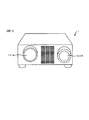
図1は、本発明の実施形態による投影装置1を前方から見た図である。図1に示すように、投影装置1の正面には、投影光学系111(図2参照)を構成する投影レンズ111Aと、撮像光学系121(図2参照)を構成する撮影レンズ121Aとが設けられている。投影装置1は、机上などに載置された状態で前方のスクリーンなどに向けて、内蔵する投射ユニット110(図2参照)から画像などを投影する。
FIG. 1 is a view of a
図2は、投影装置1の構成を説明するブロック図である。図2において投影装置1は、投射ユニット110と、撮像ユニット120と、制御回路101と、メモリ102と、操作部103と、外部インターフェイス(I/F)回路104と、メモリカードインターフェイス(I/F)105とを備え、メモリカードインターフェイス105にはメモリカード150が接続される。
FIG. 2 is a block diagram illustrating the configuration of the
制御回路101は、マイクロプロセッサおよびその周辺回路からなる。制御回路101は、制御プログラムに基づいて、投影装置内各部から入力される信号を用いて所定の演算を行う。そして、制御回路101は、演算結果を制御信号として投影装置内各部に出力し、投影装置1の投影動作および撮像動作を制御する。なお、制御プログラムは制御回路101内の不図示のROMに格納される。
The
制御回路101は画像処理部101Aを有する。画像処理部101Aでは、外部インターフェイス104を介して取得した画像データまたはメモリカード150より取得した画像データに対して画像処理を行う。画像処理部101Aで行う画像処理の詳細については後述する。
The
メモリ102は制御回路101の作業用メモリとして使用される。操作部103はボタンやスイッチなどで構成され、操作されたボタンやスイッチに対応する操作信号を制御回路101へ出力する。メモリカード150は、制御回路101の指示によりデータの書き込み、保存および読み出しが可能である。
The
投射ユニット110は、投影光学系111、液晶パネル112、LED光源113、および投射制御回路114を含む。LED光源113は、供給電流に応じた明るさで液晶パネル112を照明する。液晶パネル112は、投射制御回路114からの駆動信号に応じて光像を生成する。投影光学系111は、液晶パネル112から射出される光像を投射する。投射制御回路114は、制御回路101からの指示により、LED光源113および液晶パネル112へ制御信号を出力する。
The
投射ユニット110は制御回路101から指示された画像を投影する。投射ユニット110は、メモリカード150内に保存されている画像データの他、外部インターフェイス回路104を介して外部機器から供給される画像データによる画像を投影することができる。メモリカード150内に保存されている画像データの画像、または、外部インターフェイス回路104を介して外部機器から供給される画像データの画像を、以下、入力画像と呼ぶ。
The
撮像ユニット120は、撮像光学系121、撮像素子122および撮像制御回路123を有し、制御回路101からの指示に応じて投影面を撮像する。撮像光学系121は、撮像素子122の撮像面上に被写体像を結像させる。撮像素子122は被写体像を電気信号に変換する。撮像素子122としては、CCDやCMOS撮像素子などが用いられる。撮像制御回路123は、制御回路101からの指示により撮像素子122を駆動制御するとともに、撮像素子122から出力される電気信号に対して所定の信号処理を行う。
The
次に、制御回路101の画像処理部101Aで行われる画像処理を説明する。本発明の実施形態の画像処理では、入力画像を投影面に投射したときに投影面の模様や汚れが目立たなくなるように、撮像ユニット120により撮影した投影面の画像に基づいて、入力画像の補正を行う。
Next, image processing performed by the
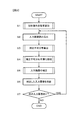
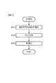
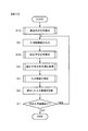
図3のフローチャートを参照して、画像処理部101Aで行う画像処理について説明する。図3の処理は、投影装置1が、投影を開始するための処理を開始するとスタートするプログラムにより画像処理部101Aにおいて実行される。
The image processing performed by the
ステップS1では、投影面の反射率を表す画像を算出する。ステップS2では、入力画像の画像データを、外部インターフェイス回路104を介して、またはメモリカード150から読み込み、メモリ102に記憶する。ステップS3では、補正不可分布を算出する。補正不可分布とは、入力画像の補正により見えないようにすることが困難である投影面の反射率の低い部分の分布である。反射率の低い部分は、投影する画像の輝度を大きく下げることなく、投影された画像を通して見えないようにすることは困難である。
In step S1, an image representing the reflectance of the projection surface is calculated. In step S <b> 2, the image data of the input image is read from the
ステップS4では、補正不可分布を平滑化する。ステップS5では、平滑化された補正不可分布および投影面の反射率を表す画像に基づいて、ステップS2で読み込んだ入力画像を補正する。ステップS6では、ステップS5で補正した入力画像をアナログ変換して、補正した入力画像を投影する。ステップS7では、次に投影する入力画像があるか否かを判定する。次に投影する入力画像がある場合はステップS7が肯定判定され、ステップS2に戻る。次に投影する入力画像がない場合はステップS7が否定判定され、画像処理を終了する。 In step S4, the uncorrectable distribution is smoothed. In step S5, the input image read in step S2 is corrected based on the smoothed uncorrectable distribution and the image representing the reflectance of the projection surface. In step S6, the input image corrected in step S5 is converted into an analog signal, and the corrected input image is projected. In step S7, it is determined whether there is an input image to be projected next. If there is an input image to be projected next, affirmative determination is made in step S7, and the process returns to step S2. If there is no input image to be projected next, a negative determination is made in step S7, and the image processing ends.
次に、図3のフローチャートのステップS1、S3、S4,S5を詳細に説明する。 Next, steps S1, S3, S4, and S5 of the flowchart of FIG. 3 will be described in detail.
−投影面の反射率を表す画像の算出−
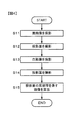
図4のフローチャートを参照して、ステップS1における投影面の反射率を表す画像の算出処理を説明する。i番目の画素値が(R,G,B)iで与えられる入力画像を投射ユニット110で投影したとき、投影面の撮影画像における、i番目の画素値に対応する画素値を(RP,GP,BP)iとする。
-Calculation of image representing reflectance of projection surface-
With reference to the flowchart of FIG. 4, the calculation process of the image showing the reflectance of the projection surface in step S1 will be described. When an input image whose i-th pixel value is given by (R, G, B) i is projected by the
ステップS11では、黒画像((R,G,B)i=(0,0,0)i)を投影面に投影する。ステップS12では、黒画像を投影した投影面を撮影する。このときの撮影画像A01の画素値を(RP,GP,BP)i=(RA01,GA01,BA01)iとする。 In step S11, a black image ((R, G, B) i = (0, 0, 0) i ) is projected onto the projection plane. In step S12, the projection plane on which the black image is projected is photographed. The pixel value of the captured image A01 at this time is (R P , G P , B P ) i = (R A01 , G A01 , B A01 ) i .
ステップS13では、白画像((R,G,B)i=(255,255,255)i)を投影面に投影する。ステップS14では、白画像を投影した投影面を撮影する。このときの撮影画像A02の画素値を(RP,GP,BP)i=(RA02,GA02,BA02)iとする。 In step S13, a white image ((R, G, B) i = (255, 255, 255) i ) is projected onto the projection plane. In step S14, the projection plane on which the white image is projected is photographed. The pixel value of the photographed image A02 at this time is (R P , G P , B P ) i = (R A02 , G A02 , B A02 ) i .
ステップS15では、撮影画像A02と撮影画像A01との差分から投影面の反射率を表す画像A03を算出する。具体的には、(RA03,GA03,BA03)i=(RA02−RA01,GA02−GA01,BA02−BA01)iの画像を算出する。 In step S15, an image A03 representing the reflectance of the projection plane is calculated from the difference between the captured image A02 and the captured image A01. Specifically, an image of (R A03 , G A03 , B A03 ) i = (R A02 −R A01 , G A02 −G A01 , B A02 −B A01 ) i is calculated.
−補正不可分布算出−
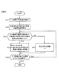
図5のフローチャートを参照して、図3のステップS3で行う補正不可分布の算出処理について説明する。
-Uncorrectable distribution calculation-
With reference to the flowchart of FIG. 5, the calculation process of the uncorrectable distribution performed in step S3 of FIG. 3 will be described.
ステップS21では、入力画像の画素値を規格化する。8ビットの画像データの場合、画素値を255で割り算する。つまり、入力画像のi番目の規格化された画素値は、(RB01,GB01,BB01)i=(R/255,G/255,B/255)iとなる。ステップS22では、投影面の反射率を表す画像の画素値を規格化する。画像A03における画素値RA03、GA03、BA03の最大値をRMAX、GMAX、BMAXとすると、投影面の反射率を表す画像A03のi番目の規格化された画素値は、(RB02,GB02,BB02)i=(R/RMAX,G/GMAX,B/BMAX)iとなる。 In step S21, the pixel value of the input image is normalized. In the case of 8-bit image data, the pixel value is divided by 255. That is, the i-th normalized pixel value of the input image is (R B01 , G B01 , B B01 ) i = (R / 255, G / 255, B / 255) i . In step S22, the pixel value of the image representing the reflectance of the projection surface is normalized. The maximum value of the pixel values R A03, G A03, B A03 in the image A03 R MAX, G MAX, When B MAX, i th normalized pixel values of the image A03 representing the reflectance of the projection plane, ( R B02 , G B02 , B B02 ) i = (R / R MAX , G / G MAX , B / B MAX ) i
ステップS23では、入力画像の規格化された画素値が、投影面の反射率を表す画像A03の規格化された画素値より大きいか否かを判定する。入力画像の規格化された画素値が、投影面の反射率を表す画像A03の規格化された画素値より大きい場合は、ステップS23が肯定判定され、ステップS24へ進む。入力画像の規格化された画素値が、投影面の反射率を表す画像A03の規格化された画素値以下の場合は、ステップS23が否定判定され、ステップS25へ進む。 In step S23, it is determined whether or not the normalized pixel value of the input image is larger than the normalized pixel value of the image A03 representing the reflectance of the projection surface. When the normalized pixel value of the input image is larger than the normalized pixel value of the image A03 representing the reflectance of the projection surface, an affirmative determination is made in step S23 and the process proceeds to step S24. If the normalized pixel value of the input image is equal to or less than the normalized pixel value of the image A03 representing the reflectance of the projection surface, a negative determination is made in step S23, and the process proceeds to step S25.
ステップS24では、補正不可分布B03(RB03,GB03,BB03)iの補正不可分布値RB03,GB03,BB03を、投影面の反射率を表す画像A03の規格化された画素値RB02,B02,BB02とする。ステップS25では、補正不可分布B03(RB03,GB03,BB03)iの補正不可分布値RB03,GB03,BB03を1とする。たとえば、入力画像のi番目の規格化された画素値が、RB01>RB02、GB01<GB02、BB01>BB02の場合、補正不可分布B03(RB03,GB03,BB03)iは、(RB02,1,BB02)iとなる。 In step S24, the uncorrectable distribution values B B03 (R B03 , G B03 , B B03 ) i of the uncorrectable distribution values R B03 , G B03 , B B03 are used as the normalized pixel values of the image A03 representing the reflectance of the projection plane. Let R B02 , B02 , B B02 . In step S25, the uncorrectable distribution values R B03 , G B03 , and B B03 of the uncorrectable distribution B03 (R B03 , G B03 , B B03 ) i are set to 1. For example, if the i-th normalized pixel value of the input image is R B01 > R B02 , G B01 <G B02 , B B01 > B B02 , the uncorrectable distribution B03 (R B03 , G B03 , B B03 ) i becomes (R B02 , 1, B B02 ) i .
ステップS26では、入力画像の全ての画素についてステップS23の比較が終了したか否かを判定する。入力画像の全ての画素についてステップS23の比較が終了した場合はステップS26が肯定判定され、補正不可分布の算出処理を終了する。入力画像の全ての画素の中にステップS23の比較が終了していないものがある場合はステップS26が否定判定され、ステップS23に戻る。 In step S26, it is determined whether or not the comparison in step S23 has been completed for all pixels of the input image. When the comparison in step S23 is completed for all the pixels of the input image, an affirmative determination is made in step S26, and the calculation process of the uncorrectable distribution is terminated. If all the pixels of the input image have not been compared in step S23, a negative determination is made in step S26, and the process returns to step S23.
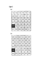
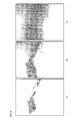
図6を参照して、補正不可分布B03の算出処理を具体的に説明する。図6(a)は、入力画像を示す図である。図6(b)は、投影面の反射率分布を示す図である。図6(a)に示す入力画像を規格化した画像B01と、図6(b)に示す反射率分布を表す画像A03を規格化した画像B02とを比較して補正不可分布B03を算出すると、図6(c)に示す補正不可分布B03となる。 The calculation process of the uncorrectable distribution B03 will be specifically described with reference to FIG. FIG. 6A shows an input image. FIG. 6B is a diagram showing the reflectance distribution on the projection surface. Comparing the image B01 normalized from the input image shown in FIG. 6A with the image B02 normalized from the image A03 representing the reflectance distribution shown in FIG. 6B, the uncorrectable distribution B03 is calculated. An uncorrectable distribution B03 shown in FIG.
−補正不可分布平滑化処理−
図7のフローチャートを参照して、図3のステップS4の補正不可分布平滑化処理を説明する。
-Uncorrectable distribution smoothing process-
With reference to the flowchart of FIG. 7, the uncorrectable distribution smoothing process in step S4 of FIG. 3 will be described.
ステップS31では、補正不可分布B03にローパスフィルタ(平滑化フィルタ)を適用して、補正不可分布の平滑化を行う。図8を参照して、3×3のカーネル(重み平均計算に用いられる局所領域)で行う補正不可分布の平滑化を例に上げて説明する。3×3の画素の中心の画素が注目画素であり、注目画素における補正不可分布値は0.3である。注目画素に隣接する画素の補正不可分布値は、1.0、0.8、1.0、0.6、0.5、0.5、0.7および0.9である。注目画素の補正不可分布値および注目画素に隣接する画素の補正不可分布値について重み平均計算を行うと、つまり、注目画素の補正不可分布値および注目画素に隣接する画素の補正不可分布値に1/9の重み付けをして足し算すると、平滑化後の注目画素の補正不可分布値は算出され、その値は0.7となる。 In step S31, a low pass filter (smoothing filter) is applied to the uncorrectable distribution B03 to smooth the uncorrectable distribution. With reference to FIG. 8, a description will be given by taking as an example the smoothing of an uncorrectable distribution performed in a 3 × 3 kernel (local region used for weighted average calculation). The pixel at the center of the 3 × 3 pixels is the target pixel, and the uncorrectable distribution value at the target pixel is 0.3. The uncorrectable distribution values of the pixels adjacent to the target pixel are 1.0, 0.8, 1.0, 0.6, 0.5, 0.5, 0.7, and 0.9. When the weighted average calculation is performed on the uncorrectable distribution value of the target pixel and the uncorrectable distribution value of the pixel adjacent to the target pixel, that is, the uncorrectable distribution value of the target pixel and the uncorrectable distribution value of the pixel adjacent to the target pixel are 1 When the weighting of / 9 is added and added, the uncorrectable distribution value of the target pixel after smoothing is calculated, and the value becomes 0.7.
なお、カーネル(重み平均計算に用いられる局所領域)の大きさは、補正した入力画像を投影したときの見え方によって、適宜選択することができる。たとえば、9×9でもよいし、13×13でもよい。また、平滑化の処理をローパスフィルタで行う代わりに、メディアンフィルタで行うようにしてもよい。 Note that the size of the kernel (the local region used for the weighted average calculation) can be appropriately selected depending on the appearance when the corrected input image is projected. For example, it may be 9 × 9 or 13 × 13. Further, the smoothing process may be performed by a median filter instead of the low pass filter.
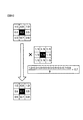
ステップS32では、平滑化した補正不可分布のブロック化を行う。以下、平滑化した補正不可分布を平滑補正不可分布と呼ぶ。平滑補正不可分布のブロック化とは、平滑補正不可分布を所定の領域で区分けし、1つの区分けした領域(1つのブロック)に含まれる画素の補正不可分布値の中で、値が最も小さい補正不可分布値をその領域に含まれる画素の補正不可分布値とする処理である。図9を参照して、6×6の画素を1つのブロックとした場合のブロック化の処理を説明する。図9(a)に示すように、6×6の画素の中で、つまり、1つのブロックの中で値が最も小さい補正不可分布値は0.5である。したがって、ブロック化の処理を行うと、図9(b)に示すように、1つのブロックに含まれる画素の補正不可分布値は、全て0.5となる。 In step S32, the smoothed uncorrectable distribution is blocked. Hereinafter, the smoothed non-correctable distribution is referred to as a smooth non-correctable distribution. Non-smooth correction distribution is divided into non-smooth correction distributions in a predetermined area, and the correction with the smallest value among the non-correctable distribution values of pixels included in one divided area (one block). This is a process of setting the impossible distribution value to the correction impossible distribution value of the pixels included in the region. With reference to FIG. 9, the process of blocking when 6 × 6 pixels are made one block will be described. As shown in FIG. 9A, the non-correctable distribution value having the smallest value in the 6 × 6 pixels, that is, in one block is 0.5. Therefore, when the blocking process is performed, as shown in FIG. 9B, all the non-correctable distribution values of the pixels included in one block are 0.5.
ステップS33では、ブロック化した平滑補正不可分布にローパスフィルタを適用して、平滑補正不可分布の平滑化を行う。この平滑化の処理におけるカーネルの大きさは、ステップS31の平滑化の処理のときのカーネルの大きさに比べて大きくする。たとえば、101×101〜201×201とする。以下、ブロック化した平滑補正不可分布をさらに平滑化したものを輝度値低下倍率分布と呼ぶ。 In step S33, a smoothing correction impossible distribution is performed by applying a low-pass filter to the blocked smooth correction impossible distribution. The kernel size in the smoothing process is set larger than the kernel size in the smoothing process in step S31. For example, 101 × 101 to 201 × 201. Hereinafter, the smoothed non-smoothable distribution that has been blocked is referred to as a luminance value reduction magnification distribution.
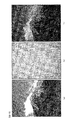
図10を参照して、補正不可分布平滑化処理を具体的に説明する。図10(a)は、図6(c)の補正不可分布を平滑した平滑補正不可分布を示す図である。平滑化するときのカーネルの大きさは9×9である。図10(b)は、図10(a)の平滑補正不可分布をブロック化したもの示す図である。1つのブロックは、20×30の画素から構成される。図10(c)は、図10(b)のブロック化した平滑補正不可分布をさらに平滑化した輝度値低下倍率分布を示す図である。 With reference to FIG. 10, the uncorrectable distribution smoothing process will be specifically described. FIG. 10A is a diagram illustrating a smooth correction impossible distribution obtained by smoothing the correction impossible distribution of FIG. The size of the kernel when smoothing is 9 × 9. FIG. 10B is a diagram showing the smooth correction impossible distribution of FIG. One block is composed of 20 × 30 pixels. FIG. 10C is a diagram illustrating a luminance value reduction magnification distribution obtained by further smoothing the blocked smooth correction impossible distribution of FIG. 10B.
−入力画像の補正−
図11のフローチャートを参照して、図3のステップS5の入力画像の補正処理について説明する。
-Correction of input image-
With reference to the flowchart of FIG. 11, the correction process of the input image in step S5 of FIG. 3 will be described.
ステップS41では、入力画像に輝度値低下倍率分布を乗算する。たとえば、入力画像のi番目の画素値が(R,G,B)iであり、輝度値低下倍率分布のi番目の画素における補正不可分布値が(α,β,γ)iである場合、入力画像に輝度値低下倍率分布を乗算した画像のi番目の画素における値は、(Rα,Gβ,Bγ)iとなる。 In step S41, the input image is multiplied by the luminance value reduction magnification distribution. For example, when the i-th pixel value of the input image is (R, G, B) i and the uncorrectable distribution value at the i-th pixel of the luminance value reduction magnification distribution is (α, β, γ) i , The value at the i-th pixel of the image obtained by multiplying the input image by the luminance value reduction magnification distribution is (Rα, Gβ, Bγ) i .
ステップS42では、入力画像に輝度値低下倍率分布を乗算した画像を、さらに投影面の反射率を表す画像で割り算する。たとえば、入力画像に輝度値低下倍率分布を乗算した画像のi番目の画素における値が(Rα,Gβ,Bγ)iであり、投影面の反射率を表す画像のi番目の画素における画素値が(RA03,GA03,BA03)iである場合、入力画像に輝度値低下倍率分布を乗算した画像を、投影面の反射率を表す画像の画素値で割り算した2つの画像の比は、(Rα/RA03,Gβ/GA03,Bγ/BA03)iとなる。この2つの画像の比を量子化して作成した画像が、入力画像を補正した画像となる。この画像が撮像装置1から投影される。
In step S42, an image obtained by multiplying the input image by the luminance value reduction magnification distribution is further divided by an image representing the reflectance of the projection plane. For example, the value of the i-th pixel of the image obtained by multiplying the input image by the luminance value reduction magnification distribution is (Rα, Gβ, Bγ) i , and the pixel value of the i-th pixel of the image representing the reflectance of the projection plane is (R A03 , G A03 , B A03 ) If i , the ratio of the two images obtained by dividing the input image multiplied by the luminance value reduction magnification distribution by the pixel value of the image representing the reflectance of the projection plane is (Rα / R A03 , Gβ / G A03 , Bγ / B A03 ) i . An image created by quantizing the ratio of these two images is an image obtained by correcting the input image. This image is projected from the
図12を参照して、入力画像の補正処理を具体的に説明する。図12(a)は、入力画像(図6(a)参照)に輝度値低下倍率分布(図10(c)参照)を乗算した画像を示す図である。図12(b)は、図12(a)の画像を投影面の反射率を表す画像(図6(b)参照)で割り算したものを表した画像である。この画像が撮像装置1から投影される。図12(c)は、図12(b)の画像を図6(b)の投影面に投影したときにユーザによって観察される観察画像である。図12(c)の観察画像では、画像のダイナミックレンジが広く、また、投影面の模様や色が目立たない。
The input image correction process will be specifically described with reference to FIG. FIG. 12A is a diagram illustrating an image obtained by multiplying the input image (see FIG. 6A) by the luminance value decrease magnification distribution (see FIG. 10C). FIG. 12B shows an image obtained by dividing the image of FIG. 12A by an image representing the reflectance of the projection plane (see FIG. 6B). This image is projected from the
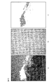
参考のために、入力画像を補正しないで投影した場合の観察画像を図13に示す。図13(a)は、入力画像を示す図であり、入力画像は、「空」を背景に撮影された山頂の画像である。図13(b)は投影面の画像である。図13(c)は、図13(a)の画像を図13(b)の投影面に投影したときにユーザによって観察される観察画像である。13(c)の観察画像では、投影面の模様が投影された画像の「空」の領域でよく見える。 For reference, an observation image when the input image is projected without correction is shown in FIG. FIG. 13A is a diagram showing an input image, and the input image is an image of a mountain peak taken against the background of “sky”. FIG. 13B is an image of the projection plane. FIG. 13C is an observation image observed by the user when the image in FIG. 13A is projected onto the projection plane in FIG. In the observation image 13 (c), the pattern on the projection surface can be seen well in the “sky” region of the projected image.
次に、図14および図15を参照して、補正された入力画像を投影面に投影したときに投影面で観察される観察画像と、補正不可分布を平滑化するときのカーネルの大きさとの関係を説明する。図14(a)は、平滑化をしない場合(カーネルの大きさがゼロの場合)の観察画像である。図14(b)は、カーネルの大きさを3×3にした場合の観察画像であり、図14(c)は、カーネルの大きさを5×5にした場合の観察画像である。図15(a)は、カーネルの大きさを9×9にした場合の観察画像であり、図15(b)は、カーネルの大きさを13×13にした場合の観察画像である。図15(c)は、カーネルの大きさを25×25にした場合の観察画像である。 Next, referring to FIG. 14 and FIG. 15, the observation image observed on the projection surface when the corrected input image is projected onto the projection surface, and the size of the kernel when smoothing the uncorrectable distribution Explain the relationship. FIG. 14A is an observation image when smoothing is not performed (when the kernel size is zero). FIG. 14B is an observation image when the kernel size is 3 × 3, and FIG. 14C is an observation image when the kernel size is 5 × 5. FIG. 15A is an observation image when the kernel size is 9 × 9, and FIG. 15B is an observation image when the kernel size is 13 × 13. FIG. 15C is an observation image when the kernel size is 25 × 25.
図14(a)に示すように、補正不可分布を平滑化しないと観察画像のダイナミックレンジが非常に狭くなり、観察画像の視認性が非常に悪くなる。図14(b)、図14(c)、図15(a)、図15(b)に示すように、補正不可分布を平滑化するときのカーネルの大きさが大きくなるにしたがって、観察画像のダイナミックレンジは広がり、観察画像の視認性が良好になる。しかし、図15(c)に示すように、カーネルの大きさが大きくなりすぎると、投影面の模様などが少し目立つようになる。 As shown in FIG. 14A, if the uncorrectable distribution is not smoothed, the dynamic range of the observation image becomes very narrow, and the visibility of the observation image becomes very poor. As shown in FIGS. 14 (b), 14 (c), 15 (a), and 15 (b), as the size of the kernel when smoothing the uncorrectable distribution increases, The dynamic range is widened and the visibility of the observed image is improved. However, as shown in FIG. 15C, when the size of the kernel becomes too large, the pattern on the projection surface becomes slightly conspicuous.
以上説明した実施形態によれば、次の作用効果が得られる。
(1)投影面の反射率分布を検出し、入力画像を入力し、検出された反射率分布を入力画像に基づいて補正し、補正された反射率分布を平滑化し、平滑化された反射率分布に基づいて入力画像を補正し、補正された入力画像を投影面に投影するようにした。これにより、投影された画像の視認性を著しく低下させることなく、投影面の色や模様に対する入力画像の補正を行うことができる。
According to the embodiment described above, the following operational effects can be obtained.
(1) The reflectance distribution of the projection surface is detected, the input image is input, the detected reflectance distribution is corrected based on the input image, the corrected reflectance distribution is smoothed, and the smoothed reflectance The input image is corrected based on the distribution, and the corrected input image is projected onto the projection plane. Thereby, it is possible to correct the input image with respect to the color and pattern of the projection surface without significantly reducing the visibility of the projected image.
(2)検出された反射率分布に基づいて、さらに入力画像を補正するようにしたので、投影面の色や模様に対する入力画像の補正を適切に行うことができる。 (2) Since the input image is further corrected based on the detected reflectance distribution, the input image can be appropriately corrected for the color and pattern of the projection plane.
(3)反射率分布補正手段によって補正された反射率分布を平滑化し、平滑化された反射率分布の中で反射率の低い領域を拡張し、反射率の低い領域が拡張された反射率分布をさらに平滑化することによって、反射率分布の平滑化を行うようにした。これにより、入力画像を補正するときに使用する、平滑化された反射率分布を適切に算出することができる。 (3) The reflectance distribution corrected by the reflectance distribution correcting means is smoothed, the low reflectance region is expanded in the smoothed reflectance distribution, and the low reflectance region is expanded. Is further smoothed to smooth the reflectance distribution. Thereby, the smoothed reflectance distribution used when correcting the input image can be appropriately calculated.
(4)反射率分布の平滑化の処理の際の低反射率領域の拡張で、平滑化された反射率分布を区分けし、区分けした領域内の反射率分布の中で低い反射率をその区分けした領域の反射率とすることにより、平滑化された反射率分布の中で反射率の低い領域を拡張するようにした。これにより、入力画像を適切に補正できるように、平滑化された反射率分布の中で反射率の低い領域を拡張することができる。 (4) The low reflectance region is expanded in the process of smoothing the reflectance distribution to classify the smoothed reflectance distribution, and the low reflectance among the reflectance distributions in the classified region is classified. By setting the reflectivity of the region, the low reflectivity region in the smoothed reflectivity distribution was expanded. Thereby, the area | region with a low reflectance can be expanded in the smoothed reflectance distribution so that an input image can be correct | amended appropriately.
(5)ブロック化した平滑反射率分布の平滑化(2回目の平滑化)における重み平均計算に用いられる局所領域は、平滑反射率分布の平滑化(1回目の平滑化)における重み平均計算に用いられる局所領域に比べて大きくするようにした。これにより、入力画像を補正して入力画像のダイナミックレンジを部分的に狭くした場合、その部分を目立たないようにすることができる。 (5) A local region used for weighted average calculation in smoothing of the smoothed reflectance distribution that has been blocked (second smoothing) is used for weighted average calculation in smoothing of the smoothed reflectance distribution (first smoothing). It was made larger than the local area used. Thereby, when the input image is corrected and the dynamic range of the input image is partially narrowed, the portion can be made inconspicuous.
(6)入力画像の規格化した画素値と、投影面の規格化した反射率とを比較して補正不可分布を算出するようにしたので、投影面の中から、投影された画像の視認性が悪くならないように補正することが困難である、反射率の低い部分を適切に抽出することができる。また、入力画像の規格化した画素値と、投影面の反射率を表す画像の規格化された画素値とを比較することによって、入力画像の規格化した画素値と、投影面の規格化した反射率との比較するようにしたので、両者の比較を簡単に行うことができる。 (6) Since the non-correctable distribution is calculated by comparing the normalized pixel value of the input image with the normalized reflectance of the projection plane, the visibility of the projected image from the projection plane is calculated. Therefore, it is possible to appropriately extract a portion with low reflectivity that is difficult to correct so as not to deteriorate. In addition, by comparing the normalized pixel value of the input image with the normalized pixel value of the image representing the reflectance of the projection plane, the normalized pixel value of the input image and the projection plane are normalized. Since the comparison with the reflectance is made, the comparison between the two can be easily performed.
以上の実施の形態を次のように変形することができる。
(1)投影面の反射率分布を表す画像を算出することによって投影面の反射率分布を検出したが、投影面の反射率分布を検出できれば、実施形態に限定されない。たとえば、投射ユニット110から投射された光の強度と、撮像ユニット120によって検出された投影面の反射光の強度とに基づいて反射率分布を検出するようにしてもよい。
The above embodiment can be modified as follows.
(1) Although the reflectance distribution of the projection plane is detected by calculating an image representing the reflectance distribution of the projection plane, the present invention is not limited to the embodiment as long as the reflectance distribution of the projection plane can be detected. For example, the reflectance distribution may be detected based on the intensity of light projected from the
(2)投影面に投影された画像のダイナミックレンジが非常に狭くならなければ、投影面の反射率分布の平滑化は、実施形態に限定されない。たとえば、ローパスフィルタを適用して投影面の反射率分布を平滑化し、その後のブロック化の処理や2度目の平滑化の処理を行わないようにしてもよい。 (2) The smoothing of the reflectance distribution on the projection surface is not limited to the embodiment unless the dynamic range of the image projected on the projection surface becomes very narrow. For example, a low-pass filter may be applied to smooth the reflectance distribution on the projection surface, and the subsequent blocking process or the second smoothing process may not be performed.
(3)平滑化された反射率分布の中で反射率の低い領域を拡張する方法は、入力画像の補正を適切に行えるように反射率の低い領域を拡張できれば、平滑された補正不可分布のブロック化に限定されない。また、入力画像の補正を適切に行えれば、平滑化された反射率分布の中で拡張する領域の反射率も実施形態に限定されない。 (3) In the method of expanding the low reflectance region in the smoothed reflectance distribution, if the low reflectance region can be expanded so that the input image can be corrected appropriately, the smoothed uncorrectable distribution It is not limited to blocking. Also, if the input image can be corrected appropriately, the reflectance of the region to be expanded in the smoothed reflectance distribution is not limited to the embodiment.
(4)入力画像の画素値を規格化するとき、入力画像の画素値の最大値で各画素の画素値を割り算することによって規格化するようにしてもよい。 (4) When normalizing the pixel value of the input image, normalization may be performed by dividing the pixel value of each pixel by the maximum value of the pixel value of the input image.
(5)入力画像の規格化した画素値と、投影面の規格化した反射率との比較を、入力画像の規格化した画素値と、投影面の反射率を表す画像の規格化された画素値とを比較することによって行ったが、入力画像の規格化した画素値と、検出した投影面の反射率を規格化したものとを比較するようにしてもよい。 (5) A comparison between the normalized pixel value of the input image and the normalized reflectance of the projection surface, and the normalized pixel value of the image representing the normalized pixel value of the input image and the reflectance of the projection surface Although the comparison is made by comparing the values, the normalized pixel value of the input image may be compared with the normalized reflectance of the detected projection surface.
(6)検出された反射率分布と、平滑化された反射率分布とに基づいて、入力画像を補正したが、入力画像に基づいて補正された反射率分布と、平滑化された反射分布とに基づいて入力画像を補正するようにしてもよい。この場合、入力画像の輝度の低い部分はあまり補正されないが、入力画像の輝度の低い部分における投影面の色や模様は目立たないので、投影された画像の視認性に問題はない。また、平滑化された反射率分布で入力画像を補正し、その補正した入力画像を、投影面の模様などの影響を抑制する従来の補正方法で補正するようにしてもよい。さらに、投影面の模様などの影響を抑制する従来の補正方法の各画素に対する補正値に、平滑化された反射率分布に基づいて重み付けを行い、その重み付けを行った補正値で入力画像を補正するようにしてもよい。 (6) Although the input image is corrected based on the detected reflectance distribution and the smoothed reflectance distribution, the corrected reflectance distribution based on the input image, and the smoothed reflectance distribution The input image may be corrected based on the above. In this case, the low-luminance portion of the input image is not corrected much, but the color and pattern of the projection surface in the low-luminance portion of the input image are not noticeable, so there is no problem in the visibility of the projected image. Alternatively, the input image may be corrected with the smoothed reflectance distribution, and the corrected input image may be corrected by a conventional correction method that suppresses the influence of the pattern on the projection surface. Furthermore, the correction value for each pixel of the conventional correction method that suppresses the influence of the pattern on the projection surface is weighted based on the smoothed reflectance distribution, and the input image is corrected with the weighted correction value. You may make it do.
(7)投影面に照射された周辺光の影響を抑制するように入力画像を補正する場合も本発明を適用することができる。この場合の適用例の概略を図16のフローチャートを参照して説明する。図16の処理は、投影装置1が、投影を開始するための処理を開始するとスタートするプログラムにより画像処理部101Aにおいて実行される。図3の処理と同様なステップについては同じ符号を付し、図3の処理と異なる部分を主に説明する。
(7) The present invention can also be applied to the case where the input image is corrected so as to suppress the influence of ambient light irradiated on the projection surface. An outline of an application example in this case will be described with reference to a flowchart of FIG. The process in FIG. 16 is executed in the
ステップS1Aでは、黒画像((R,G,B)i=(0,0,0)i)を投影した投影面を撮影して、投影面における周辺光の明るさ分布を検出する。ステップS2の次はステップS3Aに進み、ステップS3Aでは、入力画像と比較して、周辺光の明るさ分布の中で、入力画像の補正によって影響を小さくすることが困難である明るさ分布を算出する。以下、この算出した明るさ分布を補正不可分布と呼ぶ。たとえば、入力画像の画素値が、黒画像を投影した投影面を撮影した画像の画素値の所定倍以上である場合、補正不可分布値を0とする。また、入力画像の画素値が、黒画像を投影した投影面を撮影した画像の画素値の所定倍以上でない場合、補正不可分布値を、黒画像を投影した投影面を撮影した画像の画素値とする。入力画像の中で輝度の高い部分は周辺光の影響が小さく、輝度の低い部分は周辺光の影響が大きくなるからである。 In step S1A, the projection plane onto which the black image ((R, G, B) i = (0, 0, 0) i ) is projected is photographed, and the brightness distribution of the ambient light on the projection plane is detected. After step S2, the process proceeds to step S3A. In step S3A, a brightness distribution that is difficult to reduce the influence of the correction of the input image in the brightness distribution of the ambient light is calculated compared to the input image. To do. Hereinafter, this calculated brightness distribution is referred to as an uncorrectable distribution. For example, when the pixel value of the input image is equal to or greater than a predetermined value of the pixel value of the image obtained by photographing the projection surface on which the black image is projected, the uncorrectable distribution value is set to zero. In addition, when the pixel value of the input image is not equal to or larger than a predetermined value of the pixel value of the image obtained by photographing the projection surface on which the black image is projected, the correction impossible distribution value is set as the pixel value of the image obtained by photographing the projection surface on which the black image is projected. And This is because the high luminance portion of the input image is less affected by ambient light, and the lower luminance portion is more affected by ambient light.
ステップS4Aでは、図3のステップS4と同様にして補正不可分布を平滑化する。ステップS5Aでは、平滑化した補正不可分布と、周辺光の明るさ分布とに基づいて入力画像を補正する。たとえば、平滑化した補正不可分布に応じて入力画像を補正した後、周辺光の明るさ分布に応じて入力画像を補正する。1番目の補正では、平滑化した補正不可分布の中で明るい部分に対応する入力画像の輝度を高くし、平滑化した補正不可分布の中で暗い部分に対応する入力画像の輝度を低くする。2番目の補正では、周辺光の明るさ分布の中で暗い部分に対応する入力画像の輝度値を高くし、周辺光の明るさ分布の中で明るい部分に対応する入力画像の輝度を低くする。そして、ステップS6に進む。 In step S4A, the uncorrectable distribution is smoothed as in step S4 of FIG. In step S5A, the input image is corrected based on the smoothed uncorrectable distribution and the brightness distribution of the ambient light. For example, after correcting the input image according to the smoothed non-correctable distribution, the input image is corrected according to the brightness distribution of the ambient light. In the first correction, the luminance of the input image corresponding to the bright portion in the smoothed non-correctable distribution is increased, and the luminance of the input image corresponding to the dark portion in the smoothed non-correctable distribution is decreased. In the second correction, the brightness value of the input image corresponding to the dark portion in the brightness distribution of the ambient light is increased, and the brightness of the input image corresponding to the bright portion in the brightness distribution of the ambient light is decreased. . Then, the process proceeds to step S6.
実施形態と変形例の一つ、もしくは複数を組み合わせることも可能である。変形例同士をどのように組み合わせることも可能である。 It is also possible to combine one or a plurality of embodiments and modifications. It is possible to combine the modified examples in any way.
以上の説明はあくまで一例であり、本発明は上記実施形態の構成に何ら限定されるものではない。 The above description is merely an example, and the present invention is not limited to the configuration of the above embodiment.
1 投影装置
101 制御回路
101A 画像処理部
104 外部インターフェイス
105 メモリカードインターフェイス
110 投射ユニット
111A 投影レンズ
120 撮像ユニット
121A 撮影レンズ
DESCRIPTION OF
Claims (3)
入力画像を入力する画像入力手段と、
前記反射率分布検出手段によって検出された前記反射率分布の規格化された画素値と前記入力画像の対応する規格化された画素値とを比較することにより補正不可分布を算出する補正不可分布算出手段と、
前記補正不可分布算出手段によって算出された補正不可分布を所定の大きさのカーネル領域で平滑化する反射率分布平滑化手段と、
前記反射率分布平滑化手段によって平滑化された平滑補正不可分布に基づいて、前記入力画像を補正する入力画像補正手段と、
前記入力画像補正手段によって補正された入力画像を前記投影面に投影する投影手段とを備えることを特徴とする投影装置。 A reflectance distribution detecting means for detecting the reflectance distribution of the projection surface by capturing the projected black image and white image ;
An image input means for inputting an input image;
Correction impossible distribution calculation for calculating a correction impossible distribution by comparing the corresponding normalized pixel values of said detected reflectance distribution of normalized pixel value and the input image by the reflectance distribution detecting means Means,
A reflectance distribution smoothing means for smoothing the correction impossible distribution calculated by said correction impossible distribution calculating means with a predetermined size of the kernel region,
Input image correction means for correcting the input image based on the non-smooth correction distribution smoothed by the reflectance distribution smoothing means;
A projection device comprising: a projection unit that projects the input image corrected by the input image correction unit onto the projection plane.
前記反射率分布平滑化手段は、前記補正不可分布算出手段により算出された前記補正不可分布を平滑化する第1の反射率分布平滑化手段と、前記第1の反射率分布平滑化手段によって平滑化された平滑補正不可分布をブロック化し、ブロック化した領域内の反射率分布の中で低い反射率をそのブロック化した領域の反射率とすることにより、平滑化された反射率分布の中で反射率の低い領域を拡張し、この拡張された反射率分布を平滑化し、輝度値低下倍率分布を算出する第2の反射率分布平滑化手段とを有することを特徴とする投影装置。 The projection device according to claim 1,
The reflectance distribution smoothing means is smoothed by the first reflectance distribution smoothing means for smoothing the non- correctable distribution calculated by the non-correctable distribution calculating means , and the first reflectance distribution smoothing means. In the smoothed reflectance distribution, the smoothed non-correctable distribution is blocked and the lower reflectance in the reflectance distribution in the blocked area is used as the reflectance of the blocked area. A projection apparatus comprising: a second reflectance distribution smoothing unit that expands a region having low reflectance, smoothes the expanded reflectance distribution, and calculates a luminance value reduction magnification distribution .
前記第1の反射率分布平滑化手段および前記第2の反射率分布平滑化手段は、重み平均計算により反射率分布を平滑化し、前記第2の反射率分布平滑化手段における重み平均計算に用いられるカーネル領域は、前記第1の反射率分布平滑化手段における重み平均計算に用いられるカーネル領域に比べて大きいことを特徴とする投影装置。
The projection apparatus according to claim 2, wherein
The first reflectance distribution smoothing means and the second reflectance distribution smoothing means smooth the reflectance distribution by weighted average calculation and are used for weighted average calculation in the second reflectance distribution smoothing means. kernel space for a projection apparatus characterized by greater than the kernel area used for weighted mean calculation in the first reflectance distribution smoothing means.
Priority Applications (1)
| Application Number | Priority Date | Filing Date | Title |
|---|---|---|---|
| JP2008327346A JP5347488B2 (en) | 2008-12-24 | 2008-12-24 | Projection device |
Applications Claiming Priority (1)
| Application Number | Priority Date | Filing Date | Title |
|---|---|---|---|
| JP2008327346A JP5347488B2 (en) | 2008-12-24 | 2008-12-24 | Projection device |
Publications (2)
| Publication Number | Publication Date |
|---|---|
| JP2010151912A JP2010151912A (en) | 2010-07-08 |
| JP5347488B2 true JP5347488B2 (en) | 2013-11-20 |
Family
ID=42571107
Family Applications (1)
| Application Number | Title | Priority Date | Filing Date |
|---|---|---|---|
| JP2008327346A Active JP5347488B2 (en) | 2008-12-24 | 2008-12-24 | Projection device |
Country Status (1)
| Country | Link |
|---|---|
| JP (1) | JP5347488B2 (en) |
Families Citing this family (3)
| Publication number | Priority date | Publication date | Assignee | Title |
|---|---|---|---|---|
| EP3067857A1 (en) * | 2015-03-13 | 2016-09-14 | Thomson Licensing | Method and device for processing a peripheral image |
| JP6733247B2 (en) * | 2016-03-22 | 2020-07-29 | 日本電気株式会社 | Unmanned Flight Device Control System, Unmanned Flight Device Control Method, and Image Projection Device |
| JP7031698B2 (en) * | 2020-06-19 | 2022-03-08 | 日本電気株式会社 | Unmanned flight device control system and unmanned flight device control method |
Family Cites Families (5)
| Publication number | Priority date | Publication date | Assignee | Title |
|---|---|---|---|---|
| JP4120841B2 (en) * | 2003-12-10 | 2008-07-16 | 日本電気株式会社 | Projector color correction method |
| JP4981350B2 (en) * | 2006-04-27 | 2012-07-18 | キヤノン株式会社 | Image projection apparatus, image display system, control method for image projection apparatus, and control program |
| CN101512630B (en) * | 2006-08-29 | 2011-06-22 | 松下电器产业株式会社 | Image display method and image display device |
| JP5110260B2 (en) * | 2007-02-23 | 2012-12-26 | セイコーエプソン株式会社 | Projector, program, information storage medium, and image distortion correction method |
| US8964070B2 (en) * | 2007-06-21 | 2015-02-24 | Nikon Corporation | Image processing method, image processing program, image processing device, image processing system, electronic camera and electronic apparatus |
-
2008
- 2008-12-24 JP JP2008327346A patent/JP5347488B2/en active Active
Also Published As
| Publication number | Publication date |
|---|---|
| JP2010151912A (en) | 2010-07-08 |
Similar Documents
| Publication | Publication Date | Title |
|---|---|---|
| CN108200354B (en) | Control method and apparatus, imaging device, computer device, and readable storage medium | |
| CN108668093B (en) | HDR image generation method and device | |
| JP5493438B2 (en) | Projector and projected image correction program | |
| US9443323B2 (en) | Image processing apparatus, image processing method and recording medium | |
| US20210160416A1 (en) | Method for imaging controlling, electronic device, and non-transitory computer-readable storage medium | |
| CN105323474A (en) | Image capturing apparatus and control method therefor | |
| US10972676B2 (en) | Image processing method and electronic device capable of optimizing hdr image by using depth information | |
| JP2015060012A (en) | Image processing system, image processing apparatus, image processing method, image processing program, and display system | |
| US11336834B2 (en) | Device, control method, and storage medium, with setting exposure condition for each area based on exposure value map | |
| US20130120616A1 (en) | Image synthesizing apparatus, image recording method, and recording medium | |
| US20090252412A1 (en) | Image processing apparatus and image processing method | |
| US9288461B2 (en) | Apparatus and method for processing image, and computer-readable storage medium | |
| WO2017185957A1 (en) | Image processing method, image processing apparatus and display device | |
| JP5347488B2 (en) | Projection device | |
| JP7346077B2 (en) | Image processing device, image processing method and program | |
| JP6541501B2 (en) | IMAGE PROCESSING APPARATUS, IMAGING APPARATUS, AND IMAGE PROCESSING METHOD | |
| JP5273008B2 (en) | Projector and projected image correction program | |
| JP5250980B2 (en) | Projector and image correction method for the projector | |
| JP7156803B2 (en) | Video projector, video display method and video display program | |
| US20220217285A1 (en) | Image processing device, image processing method, and recording medium | |
| JP5103984B2 (en) | Image processing apparatus, imaging apparatus, and image processing program | |
| US20210152727A1 (en) | Image processing apparatus, image capturing apparatus, image processing method, and storage medium | |
| JP2011181019A (en) | Bird's-eye view image generation device | |
| JP5187351B2 (en) | Projector and projected image correction program | |
| JP2006114006A (en) | Gradation conversion device, program, electronic camera, and method thereof |
Legal Events
| Date | Code | Title | Description |
|---|---|---|---|
| A621 | Written request for application examination |
Free format text: JAPANESE INTERMEDIATE CODE: A621 Effective date: 20111216 |
|
| A521 | Request for written amendment filed |
Free format text: JAPANESE INTERMEDIATE CODE: A523 Effective date: 20120627 |
|
| A977 | Report on retrieval |
Free format text: JAPANESE INTERMEDIATE CODE: A971007 Effective date: 20130301 |
|
| A131 | Notification of reasons for refusal |
Free format text: JAPANESE INTERMEDIATE CODE: A131 Effective date: 20130312 |
|
| A521 | Request for written amendment filed |
Free format text: JAPANESE INTERMEDIATE CODE: A523 Effective date: 20130510 |
|
| TRDD | Decision of grant or rejection written | ||
| A01 | Written decision to grant a patent or to grant a registration (utility model) |
Free format text: JAPANESE INTERMEDIATE CODE: A01 Effective date: 20130723 |
|
| A61 | First payment of annual fees (during grant procedure) |
Free format text: JAPANESE INTERMEDIATE CODE: A61 Effective date: 20130805 |
|
| R150 | Certificate of patent or registration of utility model |
Ref document number: 5347488 Country of ref document: JP Free format text: JAPANESE INTERMEDIATE CODE: R150 Free format text: JAPANESE INTERMEDIATE CODE: R150 |
|
| R250 | Receipt of annual fees |
Free format text: JAPANESE INTERMEDIATE CODE: R250 |
|
| R250 | Receipt of annual fees |
Free format text: JAPANESE INTERMEDIATE CODE: R250 |
|
| R250 | Receipt of annual fees |
Free format text: JAPANESE INTERMEDIATE CODE: R250 |
|
| R250 | Receipt of annual fees |
Free format text: JAPANESE INTERMEDIATE CODE: R250 |
|
| R250 | Receipt of annual fees |
Free format text: JAPANESE INTERMEDIATE CODE: R250 |
|
| R250 | Receipt of annual fees |
Free format text: JAPANESE INTERMEDIATE CODE: R250 |
|
| R250 | Receipt of annual fees |
Free format text: JAPANESE INTERMEDIATE CODE: R250 |
|
| R250 | Receipt of annual fees |
Free format text: JAPANESE INTERMEDIATE CODE: R250 |
|
| R250 | Receipt of annual fees |
Free format text: JAPANESE INTERMEDIATE CODE: R250 |
|
| R250 | Receipt of annual fees |
Free format text: JAPANESE INTERMEDIATE CODE: R250 |