WO2012133750A1 - フレキシブルプリント回路板の接続構造 - Google Patents
フレキシブルプリント回路板の接続構造 Download PDFInfo
- Publication number
- WO2012133750A1 WO2012133750A1 PCT/JP2012/058540 JP2012058540W WO2012133750A1 WO 2012133750 A1 WO2012133750 A1 WO 2012133750A1 JP 2012058540 W JP2012058540 W JP 2012058540W WO 2012133750 A1 WO2012133750 A1 WO 2012133750A1
- Authority
- WO
- WIPO (PCT)
- Prior art keywords
- printed circuit
- circuit board
- flexible printed
- alignment
- terminal
- Prior art date
- Legal status (The legal status is an assumption and is not a legal conclusion. Google has not performed a legal analysis and makes no representation as to the accuracy of the status listed.)
- Ceased
Links
Images



Classifications
-
- H—ELECTRICITY
- H05—ELECTRIC TECHNIQUES NOT OTHERWISE PROVIDED FOR
- H05K—PRINTED CIRCUITS; CASINGS OR CONSTRUCTIONAL DETAILS OF ELECTRIC APPARATUS; MANUFACTURE OF ASSEMBLAGES OF ELECTRICAL COMPONENTS
- H05K3/00—Apparatus or processes for manufacturing printed circuits
- H05K3/36—Assembling printed circuits with other printed circuits
- H05K3/361—Assembling flexible printed circuits with other printed circuits
- H05K3/363—Assembling flexible printed circuits with other printed circuits by soldering
-
- H—ELECTRICITY
- H05—ELECTRIC TECHNIQUES NOT OTHERWISE PROVIDED FOR
- H05K—PRINTED CIRCUITS; CASINGS OR CONSTRUCTIONAL DETAILS OF ELECTRIC APPARATUS; MANUFACTURE OF ASSEMBLAGES OF ELECTRICAL COMPONENTS
- H05K1/00—Printed circuits
- H05K1/18—Printed circuits structurally associated with non-printed electric components
- H05K1/189—Printed circuits structurally associated with non-printed electric components characterised by the use of flexible or folded printed circuits
-
- H—ELECTRICITY
- H05—ELECTRIC TECHNIQUES NOT OTHERWISE PROVIDED FOR
- H05K—PRINTED CIRCUITS; CASINGS OR CONSTRUCTIONAL DETAILS OF ELECTRIC APPARATUS; MANUFACTURE OF ASSEMBLAGES OF ELECTRICAL COMPONENTS
- H05K2201/00—Indexing scheme relating to printed circuits covered by H05K1/00
- H05K2201/09—Shape and layout
- H05K2201/09009—Substrate related
- H05K2201/09045—Locally raised area or protrusion of insulating substrate
-
- H—ELECTRICITY
- H05—ELECTRIC TECHNIQUES NOT OTHERWISE PROVIDED FOR
- H05K—PRINTED CIRCUITS; CASINGS OR CONSTRUCTIONAL DETAILS OF ELECTRIC APPARATUS; MANUFACTURE OF ASSEMBLAGES OF ELECTRICAL COMPONENTS
- H05K2201/00—Indexing scheme relating to printed circuits covered by H05K1/00
- H05K2201/10—Details of components or other objects attached to or integrated in a printed circuit board
- H05K2201/10007—Types of components
- H05K2201/10128—Display
-
- H—ELECTRICITY
- H05—ELECTRIC TECHNIQUES NOT OTHERWISE PROVIDED FOR
- H05K—PRINTED CIRCUITS; CASINGS OR CONSTRUCTIONAL DETAILS OF ELECTRIC APPARATUS; MANUFACTURE OF ASSEMBLAGES OF ELECTRICAL COMPONENTS
- H05K2201/00—Indexing scheme relating to printed circuits covered by H05K1/00
- H05K2201/10—Details of components or other objects attached to or integrated in a printed circuit board
- H05K2201/10007—Types of components
- H05K2201/10151—Sensor
-
- H—ELECTRICITY
- H05—ELECTRIC TECHNIQUES NOT OTHERWISE PROVIDED FOR
- H05K—PRINTED CIRCUITS; CASINGS OR CONSTRUCTIONAL DETAILS OF ELECTRIC APPARATUS; MANUFACTURE OF ASSEMBLAGES OF ELECTRICAL COMPONENTS
- H05K2203/00—Indexing scheme relating to apparatus or processes for manufacturing printed circuits covered by H05K3/00
- H05K2203/16—Inspection; Monitoring; Aligning
- H05K2203/167—Using mechanical means for positioning, alignment or registration, e.g. using rod-in-hole alignment
Definitions
- the present invention relates to a positioning structure for connecting flexible substrates.
- liquid crystal display devices are often used as display devices.
- the signal line connected to the display device is installed in a narrow space or needs to be opened and closed, so an FPC (Flexible Print Circuit) that can be easily deformed is used. There are many.
- a liquid crystal panel unit and a backlight unit that emits planar light from the back surface of the liquid crystal panel are provided, and an FPC for transmitting a driving signal is provided for each.
- a liquid crystal display device employs a so-called touch panel, which is a touch-type input device that allows input by touching the screen.
- touch panel which is a touch-type input device that allows input by touching the screen.
- the drive signal of the contact type input device and the input information by the user An FPC used as a signal line for transmitting and receiving the above signal is also provided.
- Japanese Patent Laid-Open No. 2005-317957 includes three flexible printed circuit boards (FPCs): a first flexible printed circuit board, a second flexible printed circuit board, and a third flexible printed circuit board.
- the second and / or third flexible printed circuit board is electrically connected to the first flexible printed circuit board by hot bar soldering or connection by an anisotropic conductive film (ACF).
- ACF anisotropic conductive film
- the second and / or third flexible printed circuit board is formed with alignment marks and alignment holes with respect to the first flexible printed circuit board, and the marks and holes are aligned with each other. (Or) The third flexible printed circuit board and the first flexible printed circuit board are aligned.
- alignment marks and holes By using such alignment marks and holes, the second and / or third flexible printed circuit board and the first flexible printed circuit board can be accurately aligned, and electrical connection can be made with high accuracy. Is possible.
- Japanese Patent Laid-Open No. 2007-201008 discloses a method for positioning a flexible flat cable using a land. According to this configuration, it is possible to easily position the flexible flat cable in the cable arrangement direction.
- an object of the present invention is to provide a flexible printed circuit board alignment structure capable of performing alignment between flexible substrates and connecting the flexible substrates to each other with a simple operation.
- the present invention provides a flexible printed circuit that matches the relative positions of a main flexible printed circuit board having a land and a connecting flexible printed circuit board having a terminal electrically connected to the land at a tip portion.
- a circuit board alignment structure comprising a convex alignment part disposed on a surface of the main flexible printed circuit board and in contact with an edge of the connection flexible printed circuit board.
- the alignment can be performed with high accuracy by using the alignment portion having a simple structure. Further, a positioning jig is not necessary. Moreover, since the said alignment part contacts and suppresses the edge part of the said connection flexible printed circuit board, it can suppress that the flexible printed circuit board which aligned has shifted
- the alignment portion may include a pressing portion that contacts two sides that are not parallel to each other at the tip portion of the connection flexible printed circuit board.
- connection flexible printed circuit board includes a plurality of terminals arranged at a distal end portion, and the pressing portion includes a distal end pressing portion that presses the edge portion on the distal end side of the flexible printed circuit board. May be.
- the pressing portion may include an outer pressing portion that presses at least one outer edge portion of the terminals arranged at both ends of the plurality of terminals.
- the outer pressing part may be formed integrally with the tip pressing part.
- the presser part may include an intermediate presser part that presses an edge part facing a gap formed between at least two adjacent terminals among the plurality of terminals.
- the intermediate pressing portion may be formed integrally with the tip pressing portion.
- the alignment portion may be formed integrally with an insulating layer covering the outside of the main flexible printed circuit board.
- the alignment portion may be attached and fixed to the outside of the main flexible printed circuit board.
- FIG. 1 is an exploded perspective view of a liquid crystal display device having a flexible printed circuit board alignment structure according to the present invention.
- the liquid crystal display device A includes a backlight unit 1, a liquid crystal panel unit 2, and a touch panel unit 3, which are arranged in this order from the back side.
- flexible printed circuit boards 41, 42, and 43 including signal lines are connected to the liquid crystal panel unit 2, the backlight unit 1, and the touch panel unit 3, respectively.
- the backlight unit 1 is an illumination device that irradiates the liquid crystal panel unit 2 with planar light.
- the backlight unit 1 includes an LED mounting substrate (LED panel) 10, an LED driver (not shown), an LED (Light Emitting Diode) 11, an optical member 12 such as a diffusion plate or an optical sheet, and the like.
- the LED panel 10 has the LED 11 mounted on the mounting surface facing the liquid crystal panel unit 2.
- the LED 11 forms, for example, an LED unit in which LED chips that emit light of wavelengths of red, green, and blue (R, G, B) are gathered.
- the LED unit becomes white light as a whole by emitting light of each wavelength.
- another aspect may be sufficient.
- a white LED such as a pseudo white LED or a high color rendering white LED may be used in place of the LED unit described above, or an LED that emits light of a yellow (Y) wavelength in addition to the above RGB.
- a concentrated LED unit may be used.
- the backlight unit 1 uses an LED as a light source.
- the backlight unit 1 is not limited to this, and may be a device that can emit white light, such as a cold cathode tube.
- the liquid crystal display device A is provided with a main controller (not shown). When a drive signal is input from the controller to the LED driver, the LED driver drives the LED 11 and planar light is emitted from the backlight unit 1.
- the backlight unit 1 is connected to a second flexible printed circuit board 42 for sending a drive signal from the main controller to the LED driver.
- the liquid crystal panel unit 2 includes a liquid crystal panel 21 in which liquid crystal is sealed, and a polarizing plate 22 attached to the front surface (observer side) and back surface (backlight unit 2 side) of the liquid crystal panel 21.
- the liquid crystal panel 21 includes an array substrate including a switching element such as a TFT (thin film transistor), a counter substrate disposed to face the array substrate, and a liquid crystal filled between the array substrate and the counter substrate. .
- the liquid crystal panel unit 2 also includes a liquid crystal driver that transmits a panel drive signal to the switching element (all not shown).
- a voltage is applied between the array substrate and the counter substrate in each pixel of the liquid crystal panel 21 by sending a panel drive signal to the switching element of the array substrate.
- the voltage between the array substrate and the counter substrate is changed to change the light transmittance in each pixel.
- the light of the red (R) wavelength, the light of the green (G) wavelength, and the light of the blue (B) wavelength transmitted through the liquid crystal panel 21 is mixed and mixed to obtain a desired color light (appears as a desired color). Light).
- an image is displayed on the image display unit on the viewer side of the liquid crystal panel 21.
- the liquid crystal panel unit 2 is connected to a first flexible printed circuit board 41 for sending a drive signal from the main controller to the liquid crystal driver.
- the touch panel unit 3 is superimposed on the front surface of the liquid crystal panel unit 2, and a touch operation screen corresponding to an operation selection instruction displayed on the liquid crystal panel 21, for example, a bar or a key switch,
- This is an input device that controls the liquid crystal display device by contacting a dedicated contact tool (such as a touch pen).
- the content of the touch operation screen displayed on the liquid crystal panel 21 becomes a switch, and an intuitive operation can be performed.
- a touch panel unit 3 visibility and operability are improved.
- various functions can be controlled.
- Touch panel unit 3 detects the coordinate data of the part touched by the finger or touch pen and sends it to the main controller. Then, the main controller refers to the touch operation screen displayed on the liquid crystal panel 21 and the coordinate data, determines the touched key, and determines the operation assigned to the key.
- the touch panel unit 3 an electromagnetic induction type, an electric resistance type, a capacitance type, a pressure sensitive type, and the like are known, and any of them is supplied with driving power.
- the touch panel unit 3 is connected to a third flexible printed circuit board 43 for transmitting coordinate data to the main controller.
- the first flexible printed circuit board 41 (main flexible printed circuit board) is provided with a connector 412, and is connected to a main controller (not shown) via the connector 412.
- the connector 412 can be shared by the three flexible printed circuit boards 41, 42, and 43, it is possible to save time and labor when the liquid crystal display device A is assembled to an electronic device. Therefore, in the liquid crystal display device A, when the backlight unit 1, the liquid crystal panel unit 2, and the touch panel unit 3 are assembled, the second flexible printed circuit board 42 and the third flexible printed circuit board 43 are replaced with the first flexible printed circuit board 41. Connected. In FIG. 1, the second flexible printed circuit board 42 (connected flexible printed circuit board) is connected to the left side of the connector 412, and the third flexible printed circuit board 43 (connected flexible printed circuit board) is connected to the right side of the connector 412.
- the backlight unit 1 to which the second flexible printed circuit board 42 is connected is disposed on the back side of the liquid crystal panel unit 2 to which the first flexible printed circuit board 41 is connected.
- the first flexible printed circuit board 41 is fixed to the front side.
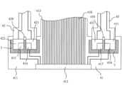
- FIG. 2 is a diagram illustrating a state in which the second and third flexible printed circuit boards are connected to the first flexible printed circuit board.
- the flexible printed circuit board will be described.
- a circuit wiring formed of a conductor such as copper foil is covered with a cover lay formed of an insulator such as polyimide.
- the coverlay is removed at the part of the terminal connected to other boards, etc., and the terminals can be electrically connected to external electronic components, other boards (including flexible printed circuit boards), etc. It has become.
- the first flexible printed circuit board 41 includes a signal line 410, a rectangular main body 411, a connector 412 mounted on the main body 411, and a large number of signal lines 410 formed integrally with the main body 411. And a connection portion 413 connected to the liquid crystal panel unit 2.
- lands 414 and 415 to which the terminals 421 and 422 of the second flexible printed circuit board 42 are connected are provided at the left end of the main body.
- lands 416 and 417 to which the terminals 431 and 432 of the third flexible printed circuit board 43 are connected are provided at the right end of the main body.
- alignment portions 5 for aligning the second flexible printed circuit board 42 and the third flexible printed circuit board 43 are formed at the left and right ends of the main body 411.
- the alignment portion 5 is a convex portion formed on the surface of the first flexible printed circuit board 41 and protruding in the thickness direction of the first flexible printed circuit board 41.
- the alignment portion 5 is formed by multilayering coverlays to increase the thickness.
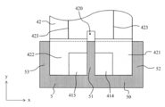
- FIG. 3 is an enlarged view of an example of the alignment structure of the flexible printed circuit board according to the present invention. Since the alignment structure of the second flexible printed circuit board 42 and the first flexible printed circuit board 41 of the third flexible printed circuit board 43 is substantially the same, the first flexible printed circuit board will be representatively described below. The alignment structure of 41 and the second flexible printed circuit board 42 will be described as an example. In FIG. 3, the horizontal direction is assumed to be the x direction, and the vertical direction is assumed to be the y direction. The following description is the same.
- the second flexible printed circuit board 42 includes a signal line 423 and a first terminal 421 and a second terminal 422 to which end portions of the signal line 423 are connected.
- the first terminal 421 and the second terminal 422 are arranged side by side in a direction perpendicular to the longitudinal direction of the second flexible printed circuit board 42, and a short circuit is caused between the first terminal 421 and the second terminal 422.
- a recess 420 is formed for suppression.
- the signal line 423 is covered with a cover lay, but the first terminal 421 and the second terminal 422 are exposed from the cover lay. Further, when the first flexible printed circuit board 41 and the second flexible printed circuit board 42 are stacked in the thickness direction, the first terminal 421 and the second terminal 422 are at least part of the first land 414 and the second land 415. Has a shape in which corners that are close to each other are notched so as to be exposed to the outside (see FIG. 3). Note that the shapes of the first terminal 421 and the second terminal 422 are not limited to this, for example, a notch formed in a portion other than the adjacent corner portion, and a half formed in an intermediate portion of one side. It is good also as a shape which provided the circular notch and the through-hole.
- first flexible printed circuit board 41 and the second flexible printed circuit board 42 are stacked in the thickness direction as the first terminal 421 and the second terminal 422, at least a part of the first land 414 and the second land 415. Can be widely used as it is exposed to the outside and can be easily soldered, as will be described later.
- the first terminal 421 is electrically connected to the first land 414 exposed from the notch by soldering.
- the second terminal 422 is also electrically connected to the second land 415 exposed from the notch by soldering. Different signals are sent to the first terminal 421 and the second terminal 422 (for example, one is an input signal and the other is an output signal). Therefore, a recess 420 is formed so that the solder connecting the first terminal 421 and the second land 414 and the solder connecting the second terminal 422 and the second land 415 are not short-circuited.
- the alignment unit 5 is a member that causes the second flexible printed circuit board 42 to contact and accurately overlaps the first terminal 421 and the second terminal 422 with the first land 414 and the second land 415, respectively.
- the alignment unit 5 includes a main body part 50 (tip pressing part) extending in the x direction, an intermediate pressing part 51 extending in the y direction from the center of the main body part 50 in the x direction, and a right end in the x direction.
- a second presser part 52 (outer presser part) extending in the y direction from the part, and a third presser part 53 (outer presser part) extending in the y direction from the left end part in the x direction.
- the first land 414 is disposed inside a region formed by the intermediate presser portion 51, the second presser portion 52, and the main body portion 50.
- the second land 415 is disposed inside an area formed by the intermediate presser portion 51, the third presser portion 53, and the main body portion 50.
- the alignment of the second flexible printed circuit board 42 with respect to the first flexible printed circuit board 41 is performed by bringing the first terminal 421 and the second terminal 422 at the tip of the second flexible printed circuit board 42 in the y direction into contact with the alignment unit 5. Done. That is, the y-direction tip portions of the first terminal 421 and the second terminal 422 of the first flexible printed circuit board 41 are in contact with the main body 50 of the alignment unit 5. At the same time, the outer edge of the first terminal 421 is in contact with the second presser 52 and the outer edge of the second terminal 422 is in contact with the third presser 53. Further, the intermediate pressing portion 51 is disposed in the concave portion 420 of the second flexible printed circuit board 42, and contacts the inner edge portion of the first terminal 421 and the inner edge portion of the second terminal 422.
- the intermediate presser portion 51 has a shape in which the tip in the y direction can reach farther than the cutout portions of the first terminal 421 and the second terminal 422.
- the intermediate presser 51 only needs to be able to press the center portion of the second flexible printed circuit board 42. If the size of the cutout portion of the first terminal 421 and the cutout portion of the second terminal 422 are different, at least Any shape can be used as long as the tip in the y direction can reach the back rather than the cutout portion of one terminal.
- the first terminal 421 and the second terminal 422 are brought into contact with the alignment unit 5, and the second flexible printed circuit board 42 is overlaid on the first flexible printed circuit board 41.
- the second terminal 422 can be aligned with the land 414 with high accuracy, respectively.
- the first flexible printed circuit board 41 and the second flexible printed circuit board 42 are electrically connected by soldering the first terminal 421 and the first land 414, and the second terminal 422 and the second land 415. Can connect. Accordingly, the first terminal 421 and the second terminal 422 can transmit and receive signals via the connector 412 and the signal line 410.
- the second flexible print The circuit board 42 can be aligned with the first flexible printed circuit board 41. For this reason, a jig is not required for alignment between the first flexible printed circuit board 41 and the second flexible printed circuit board 42. Further, the work itself is a simple work and is less likely to vary.
- the movement of the first terminal 421 and the second terminal 422 of the second flexible printed circuit board 42 is restricted by contacting each part of the alignment unit 5.
- the relative positions of the first flexible printed circuit board 41 and the second flexible printed circuit board 42 are not easily displaced after alignment. Accordingly, the first terminal 421 and the first land 414 and the second terminal 422 and the second land 415 can be easily connected.
- the intermediate presser 51 is disposed between the soldered portion between the first terminal 421 and the first land 414 and the soldered portion between the second terminal 422 and the second land 415, the soldering accuracy is increased. Even if there is variation in the thickness, it is possible to suppress the contact of overflowing solder. Thereby, it is possible to suppress a short circuit between the first terminal 421 (and the first land 414) and the second terminal 422 (and the second land 415).
- third flexible printed circuit board 43 and the first flexible printed circuit board 41 can similarly be adjusted in relative position and electrically connected.
- the second flexible printed circuit board 42 and the third flexible printed circuit board 43 can be positioned at an accurate position with respect to the first flexible printed circuit board 41 by using the alignment unit 5. At the same time, it is possible to prevent the position from shifting, so that the connection work can be easily performed.
- the alignment and connection of the first flexible printed circuit board 41 and the third flexible printed circuit board 43 have the same effect.
- the connector 412 is connected to the main controller when the liquid crystal display device A is attached to the electronic device.
- the liquid crystal display device can be easily assembled.
- the main body unit 50, the intermediate presser unit 51, the second presser unit 52, and the third presser unit 53 are integrally formed. You may be comprised by two convex parts. For example, only the main body 50 and the intermediate presser 51 may be integrated, and the second presser 52 and the third presser 53 may be separate from the main body 50.
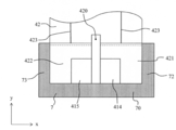
- FIG. 4 is an enlarged view of another example of a flexible printed circuit board alignment structure according to the present invention.
- the first flexible printed circuit board 41 includes an alignment unit 6.
- the alignment unit 6 includes a main body 60 extending in the x direction and an intermediate presser 61 extending in the y direction from the central portion of the main body 60.
- Alignment of the first flexible printed circuit board 41 and the second flexible printed circuit board 42 is performed as follows.
- the intermediate pressing portion 61 is disposed in the concave portion 420, and the tip portions in the y direction of the first terminal 421 and the second terminal 422 are brought into contact with the main body portion 50.
- the first terminal 421 is aligned at a predetermined position with the edge on the tip end side in the y direction being restricted to the main body 50 and the edge on the concave side being restricted to the intermediate presser 61, and is aligned with the first land 414. Overlapping directions.
- the second terminal 422 is aligned at a predetermined position by restricting the edge portion on the tip end side in the y direction to the main body portion 50 and the edge portion on the concave portion side to the intermediate presser portion 61, so that the second land 422 is aligned. It overlaps with 415 in the thickness direction.
- the movement of the first terminal 421 and the second terminal 422 of the second flexible printed circuit board 42 is restricted by contacting each part of the alignment unit 6. For this reason, the relative positions of the first flexible printed circuit board 41 and the second flexible printed circuit board 42 are not easily displaced after alignment. Accordingly, the first terminal 421 and the first land 414 and the second terminal 422 and the second land 415 can be easily connected.
- the intermediate presser 61 is disposed between the soldered portion between the first terminal 421 and the first land 414 and the soldered portion between the second terminal 422 and the second land 415, the soldering accuracy is increased. Even if there is variation in the thickness, it is possible to suppress the contact of overflowing solder. Thereby, it is possible to suppress a short circuit between the first terminal 421 (and the first land 414) and the second terminal 422 (and the second land 415).
- the first flexible printed circuit board 41 and the second flexible printed circuit board 41 and the second flexible printed circuit board 42 can be combined with the first flexible printed circuit board 41 and the second flexible printed circuit board 42 as long as the accuracy on the recessed side of the first terminal 421 and the recessed side of the second terminal 422 is high. 2 Positioning of the flexible printed circuit board 42 can be performed with high accuracy. Therefore, there are few restrictions (with respect to a dimension and a shape) at the time of manufacture of the 2nd flexible printed circuit board 42, and it is possible to make manufacture and alignment easy.
- the alignment of the third flexible printed circuit board 43 and the first flexible printed circuit board 41 can be performed in the same manner.
- the second flexible printed circuit board 42 includes the first terminal 421 and the second terminal 422.
- the present invention is not limited to this. It may be configured to have many terminals. At this time, it is possible to obtain the same effect as described above by providing the positioning portions 5 and 6 with the number of intermediate pressing portions 51 and 61 corresponding to the number of concave portions formed between the terminals. It is.
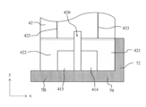
- FIG. 5 is an enlarged view of still another example of a flexible printed circuit board alignment structure according to the present invention.
- the first flexible printed circuit board 41 includes an alignment unit 7.
- the alignment unit 7 includes a main body 70 and a second presser 72 and a third presser 73 that extend in the y direction from both ends of the main body 70 in the x direction.
- the first flexible printed circuit board 41 and the second flexible printed circuit board 42 are aligned with each other by bringing the first terminal 421 and the second terminal 422 into contact with the main body portion 70 at the edge on the tip side in the y direction.
- the edge of the one terminal 421 on the outer side in the x direction (opposite to the recess) is the second presser part 72, and the outer edge of the second terminal 422 in the x direction (opposite to the recess) is the third presser part 73.
- the first terminal 421 is positioned at a predetermined position because the edge on the tip end side in the y direction is restricted to the main body part 70 and the outer side in the x direction is restricted to the second presser part 72. Overlapping directions.
- the second terminal 422 is aligned at a predetermined position because the edge on the tip end side in the y direction is regulated by the main body 70 and the outer side in the x direction is regulated by the third presser 73. And overlap in the thickness direction.
- the movement of the first terminal 421 and the second terminal 422 of the second flexible printed circuit board 42 is regulated by contacting each part of the alignment unit 7. For this reason, the relative positions of the first flexible printed circuit board 41 and the second flexible printed circuit board 42 are not easily displaced after alignment. Accordingly, the first terminal 421 and the first land 414 and the second terminal 422 and the second land 415 can be easily connected.
- the first flexible printed circuit board 41 and the second flexible printed circuit board 41 can be used.
- the printed circuit board 42 can be accurately aligned. Therefore, there are few restrictions (with respect to a dimension and a shape) at the time of manufacture of the 2nd flexible printed circuit board 42, and it is possible to make manufacture and alignment easy.
- the alignment of the third flexible printed circuit board 43 and the first flexible printed circuit board 41 can be performed in the same manner.
- FIG. 6 is a diagram showing a modification of the third embodiment.
- the alignment unit 7 ⁇ / b> B may include a main body unit 70 and a second presser unit 72.
- the alignment portion 7B having this configuration is used, the edge portions on the tip side in the y direction of the first terminal 421 and the second terminal 422 of the second flexible printed circuit board 42 are regulated by the main body portion 70.
- the edge of the first terminal 421 in the x direction is pressed by the second pressing portion 52 and is aligned at a predetermined position (a position that overlaps the first land 414 with high accuracy).
- the first terminal 421 can be soldered to the first land 414 with high accuracy.
- the alignment portion 7B does not have a member for pressing the edge portion (both the concave portion side and the outer side) in the x direction of the second terminal 422, but the second terminal 422 is obtained by aligning the first terminal 421. Are also aligned within a certain range. As a result, the second terminal 422 is also arranged at a position overlapping the second land 415 with little position adjustment without adjusting the position. Accordingly, the second terminal 422 can be accurately connected to the second land 415 without performing a difficult operation. In addition, since the alignment part 7B has a simple shape, manufacture is easy.
- the alignment of the third flexible printed circuit board 43 and the first flexible printed circuit board 41 can be performed in the same manner.
- the alignment portions 5, 6, 7, and 7 ⁇ / b> B are provided on the surface that fixes the second flexible printed circuit board 42 and the third flexible printed circuit board 43 of the first flexible printed circuit board 41. It is the formed convex part.
- the projecting amount of the convex portion is not limited as long as the second flexible printed circuit board 42 and the third flexible printed circuit board 43 are caught by the second flexible printed circuit board 43 and the movement thereof is restricted. The thing more than the thickness of the printed circuit board 42 and the 3rd flexible printed circuit board 43 is preferable.
- the present invention is not limited thereto, and for example, it may be produced by attaching a polyethylene terephthalate tape.
- a material having an insulating property and capable of forming the above-described convex portion can be widely used.
- FIG. 7 is an enlarged view of still another example of a flexible printed circuit board alignment structure according to the present invention.
- the first flexible printed circuit board 41 includes an alignment unit 8.
- the alignment unit 8 includes a main body unit 80 and a second presser unit 82 extending in the y direction.
- the main body 80 is formed adjacent to the y-direction end of the second land 415, and the second pressing portion 82 is adjacent to the x-direction outer end of the first land 414. Is formed. And the main-body part 80 and the 2nd presser part 82 are arrange
- the alignment unit 8 is an insulating member fixed to the surface of the first flexible printed circuit board 41.
- a conventionally well-known method such as adhesion or welding is used.
- an electronic component that is not used for the land may be mounted by soldering. In that case, it is preferable that parts other than the terminal of an electronic component are formed with the material (for example, resin material) which has insulation.
- the second flexible printed circuit board 42 brings the edge of the first terminal 421 on the outer side in the x direction into contact with the second pressing part 72 and the edge of the second terminal 422 on the tip side in the y direction on the main body 80. Make contact. Thereby, the movement of the first terminal 421 in the x direction is restricted, and the movement of the second terminal 422 in the y direction is restricted. Since the first terminal 421 and the second terminal 422 are integrally formed on the second flexible printed circuit board 42, the first terminal 421 is restricted in the x direction and the second terminal 422 is restricted in the y direction.
- the terminal 421 can overlap the first land 414 and the second terminal 422 can overlap the second land 415.
- the alignment accuracy is higher than when the first terminal 421 and the second terminal 422 are restricted from moving in both the x and y directions. Although it may fall, since it does not shift
- the flexible printed circuit already produced is formed by fixing a member having a shape determined by a joining method such as adhesion and welding to the first flexible printed circuit board 41. It can also be used for plates. Further, the second flexible printed circuit board 42 can be aligned to some extent even if the accuracy in the x direction and the y direction is not high.
- the alignment of the third flexible printed circuit board 43 and the first flexible printed circuit board 41 can be performed in the same manner. Further, as an example of the structure in which the alignment portion is a separate body, the alignment portion 8 as shown in FIG. 7 has been described as an example. However, the present invention is not limited to this. A member having the same shape as the described alignment portion may be produced and fixed to the first flexible printed circuit board.
- the second flexible printed circuit board 42 and the third flexible printed circuit board 43 are described as having two terminals as an example, but the present invention is not limited to this.
- the positioning structure of the flexible printed circuit board according to the present invention can be employed in an electronic device (a mobile phone, a portable information terminal, a digital camera, a personal computer, etc.) using a module including a plurality of flexible printed circuit boards.
- LED mounting board (LED panel) 11 LED 2 Liquid crystal panel unit 21 Liquid crystal panel 22 Polarizing plate 3 Touch panel unit 41 First flexible printed circuit board 411 Main body part 412 Connector 413 Connection part 414 First land 415 Second land 42 Second flexible printed circuit board 421 First terminal 422 Second Terminal 5 Positioning section 50 Main body section 51 Intermediate presser section 52 Second presser section 53 Third presser section
Landscapes
- Engineering & Computer Science (AREA)
- Manufacturing & Machinery (AREA)
- Microelectronics & Electronic Packaging (AREA)
- Combinations Of Printed Boards (AREA)
Abstract
ランド414、415を備えた主フレキシブルプリント回路板41と、ランド414、415に電気的に接続される端子421、422を先端部に備えた接続フレキシブルプリント回路板42との相対位置を合わせるフレキシブルプリント回路板の位置合わせ構造であって、主フレキシブルプリント回路板41の表面に配置され、接続フレキシブルプリント回路板42の辺縁部と接触する凸形状の位置合わせ部5を備えている。
Description
本発明は、フレキシブル基板同士を接続するときの位置決め構造に関するものである。
携帯電話機、携帯情報端末、パーソナルコンピュータ等の電子機器では、ディスプレイ装置として液晶表示装置が用いられていることが多い。上述のような電子機器において、ディスプレイ装置に接続される信号線は、設置場所が狭小であったり、開閉が必要であったりすることから、変形が容易なFPC(Flexible Print Circuit)が用いられることが多い。
例えば、液晶表示装置の場合、液晶パネルユニットと、前記液晶パネルの背面より面状光を照射するバックライトユニットとを備えており、それぞれに駆動用の信号を送信するためのFPCを備えている。
液晶表示装置には、画面に触れることで入力が可能な接触式入力装置、いわゆる、タッチパネルが採用されていることが多くなっている。前記接触式入力装置を備えた液晶表示装置では、上述の液晶パネルユニット、バックライトユニットの駆動用の信号線として用いられるFPCに加えて、前記接触式入力装置の駆動信号及び使用者による入力情報の信号を送受信するための信号線として用いられるFPCも備えられている。
前記ディスプレイ装置では、前記電子機器への組み付け時の配線の接続を容易にするため、複数のFPCを電気的にまとめることが主流となっている。例えば、特開2005-317957号公報では、第一フレキシブルプリント回路板、第ニフレキシブルプリント回路板、第三フレキシブルプリント回路板の3個のフレキシブルプリント回路板(FPC)を備えている。第ニ及び(又は)第三フレキシブルプリント回路板が、ホットバー方式はんだ付けや異方性導電膜(ACF)による接続で第一フレキシブルプリント回路板に電気的に接続されている。
そして、第二及び(又は)第三フレキシブルプリント回路板を第一フレキシブルプリント回路板に対して位置合わせ用のマークや位置合わせ用孔を形成し、そのマークや孔をあわせることで、第二及び(又は)第三フレキシブルプリント回路板と第一フレキシブルプリント回路板との位置合わせを行っている。このような、位置合わせ用のマークや孔を用いることで、第二及び(又は)第三フレキシブルプリント回路板と第一フレキシブルプリント回路板とを正確に位置合わせでき、電気的な接続を精度良く行うことが可能である。
また、特開2007-201008号公報には、ランドを利用してフレキシブルフラットケーブルの位置決めを行うものが開示されている。この構成によると、フレキシブルフラットケーブルのケーブル並び方向の位置決めを容易に、行うことが可能である。
しかしながら、特開2005-317957号公報に示すように、位置合わせマークでFPCの位置合わせを行う場合、目視による位置決め作業が必要であり、作業者によって作業にバラツキが出やすく、位置決めの精度が低下したり、位置決めの作業に時間を要したりする場合がある。また、一度位置決めを完了した後の移動を抑制するため、FPCを保持するもの(例えば、粘着テープ等)が必要である。
位置合わせ用孔を用いる場合、孔に冶具を貫通させ、その冶具に各FPCの位置合わせ用孔を外嵌させれば良く、作業者による作業のバラツキを抑えるとともに、位置決め後のFPCの移動も抑制される。しかしながら、FPCに位置合わせ用孔を必要とするとともに、位置合わせ用孔を貫通する冶具が必要となる。
また、特開2007-201008号公報に示す構成では、フレキシブルフラットケーブルの位置決めは、ランドで行うことが可能であるが、その後の移動を規制することが難しく、移動を抑制するための部材(両面テープ)が必要である。そのため、両面テープを貼着するためのスペースが必要である。また、両面テープは、フレキシブルフラットケーブルの位置決めが完了していないときでも、被接着部に接着してしまうことがあり、位置決め作業が煩雑になることが考えられる。
そこで本発明は、簡単な作業で、フレキシブル基板同士の位置合わせを行うとともに、互いのフレキシブル基板を接続することができるフレキシブルプリント回路板の位置合わせ構造を提供することを目的とする。
上記目的を達成するため本発明は、ランドを備えた主フレキシブルプリント回路板と、前記ランドに電気的に接続される端子を先端部に備えた接続フレキシブルプリント回路板との相対位置を合わせるフレキシブルプリント回路板の位置合わせ構造であって、前記主フレキシブルプリント回路板の表面に配置され、前記接続フレキシブルプリント回路板の辺縁部と接触する凸形状の位置合わせ部を備えたことを特徴とする。
この構成によると、フレキシブルプリント回路板同士の位置合わせを行うとき、簡単な構造の位置合わせ部を利用することで、精度良く位置合わせを行うことができる。また、位置合わせ用の冶具も必要ない。また、前記位置合わせ部は、前記接続フレキシブルプリント回路板の辺縁部と接触して抑えるので、位置合わせを行ったフレキシブルプリント回路板がずれるのを抑制することが可能である。
このことから、簡単な作業で位置合わせを行うことができるとともに、フレキシブルプリント回路板同士を接続することが可能である。これにより、作業精度のバラツキが発生しにくく、配線不良等の不具合が発生しにくい。
上記構成において、前記位置合わせ部は、前記接続フレキシブルプリント回路板の先端部の互いに平行でない2辺と接触する押え部を備えていてもよい。
上記構成において、前記接続フレキシブルプリント回路板は先端部に前記端子が複数個配列されており、前記押え部が、前記フレキシブルプリント回路板の前記先端側の辺縁部を押える先端押え部を含んでいてもよい。
上記構成において、前記押え部は、前記複数個の端子のうち両端に配置された端子の少なくとも一方の外側の辺縁部を押える外側押え部を含んでいてもよい。
前記外側押え部は、前記先端押え部と一体に形成されていてもよい。
上記構成において、前記押え部が、前記複数個の端子のうち少なくとも隣り合う2個の端子の間に形成された間隙に面した辺縁部を押える中間押え部を含んでいてもよい。
上記構成において、前記中間押え部が、前記先端押え部と一体に形成されていてもよい。
上記構成において、前記位置合わせ部が前記主フレキシブルプリント回路板の外部を被覆する絶縁層と一体に形成されていてもよい。
上記構成において、前記位置合わせ部が前記主フレキシブルプリント回路板の外部に取り付け固定されていてもよい。
本発明によると、簡単な作業で、フレキシブル基板同士の位置合わせを行うとともに、互いのフレキシブル基板を接続することができるフレキシブルプリント回路板の位置合わせ構造を提供することができ、これにより、接続のバラツキを抑えることができる。
以下に本発明の実施形態について図面を参照して説明する。
(第1の実施形態)
図1は本発明にかかるフレキシブルプリント回路板の位置合わせ構造を備える液晶表示装置の分解斜視図である。図1に示すように、液晶表示装置Aは、バックライトユニット1、液晶パネルユニット2及びタッチパネルユニット3を備えており、背面側からこの順番で並んで配置されている。また、図1に示すように、液晶パネルユニット2、バックライトユニット1及びタッチパネルユニット3には、それぞれ、信号線を含むフレキシブルプリント回路板41、42、43が接続されている。
図1は本発明にかかるフレキシブルプリント回路板の位置合わせ構造を備える液晶表示装置の分解斜視図である。図1に示すように、液晶表示装置Aは、バックライトユニット1、液晶パネルユニット2及びタッチパネルユニット3を備えており、背面側からこの順番で並んで配置されている。また、図1に示すように、液晶パネルユニット2、バックライトユニット1及びタッチパネルユニット3には、それぞれ、信号線を含むフレキシブルプリント回路板41、42、43が接続されている。
バックライトユニット1は、面状光を液晶パネルユニット2に照射する照明装置である。バックライトユニット1は、LED実装基板(LEDパネル)10、LEDドライバ(不図示)、LED(Light Emitting Diode:発光ダイオード)11、拡散板や光学シート等の光学部材12等を備えている。バックライトユニット1において、LEDパネル10は液晶パネルユニット2に向く実装面にLED11が実装されている。
LED11は例えば、赤、緑、青(R、G、B)の波長の光を出射するLEDチップを集結したLEDユニットを形成している。なお、LEDユニットは各波長の光が出射されることにより、全体として白色光となる。また、LED11の構成(種類、色及び組み合わせ等)については、他の態様であってもよい。例えば、上述したLEDユニットの変わりに疑似白色LEDや高演色白色LED等の白色LEDが用いられていてもよいし、上述のRGBに加えて、黄色(Y)の波長の光を出射するLEDが集結したLEDユニットが用いられてもよい。
なお、バックライトユニット1は、光源としてLEDを用いるものとしているが、これに限定されるものではなく、白色光を出射できるもの、例えば、冷陰極管等であってもよい。
液晶表示装置Aには不図示のメインコントローラが備えられており、コントローラからLEDドライバに駆動信号が入力されることで、LEDドライバがLED11を駆動し、バックライトユニット1から面状光が出射される。また、バックライトユニット1には、メインコントローラからLEDドライバに駆動信号を送るための第2フレキシブルプリント回路板42が接続されている。
液晶パネルユニット2は、液晶が封入された液晶パネル21と、液晶パネル21の前面(観察者側)及び背面(バックライトユニット2側)に貼り付けられた偏光板22とを有している。液晶パネル21は、TFT(薄膜トランジスタ)等のスイッチング素子を含むアレイ基板と、アレイ基板と対向して配置された対向基板と、アレイ基板と対向基板との間に充填される液晶とを含んでいる。また、液晶パネルユニット2は、スイッチング素子にパネル駆動信号を送信する液晶ドライバも備えている(いずれも不図示)。
アレイ基板のスイッチング素子にパネル駆動信号を送ることで、液晶パネル21の各画素におけるアレイ基板と対向基板との間に電圧が印加される。アレイ基板と対向基板の間の電圧が変化させて、各画素での光の透過度合を変更している。液晶パネル21を透過する赤色(R)波長の光、緑色(G)波長の光、青色(B)波長の光の透過度合を変更して混色し、所望の色の光(所望の色に見える光)を出射する。これにより、液晶パネル21の観察者側の画像表示部に画像を表示する。
液晶パネルユニット2は、メインコントローラから液晶ドライバに駆動信号を送るための第1フレキシブルプリント回路板41が接続されている。
タッチパネルユニット3は、液晶パネルユニット2の前面に重ね合わされるものであり、液晶パネル21に表示される動作選択の指示に応じたタッチ操作画面、例えば、バーやキースイッチ等に使用者の指或いは専用の接触具(タッチペン等)が接触することで、液晶表示装置のコントロールを行う入力装置である。
タッチパネルユニット3を備えた液晶表示装置では、液晶パネル21に表示されたタッチ操作画面の内容そのものがスイッチとなり、直感的な操作が行える。このようなタッチパネルユニット3を用いることで、視認性と操作性とが向上する。また、液晶パネル21に表示されるタッチ操作画面を切り換えることで、多彩な機能をコントロールすることが可能となる。
タッチパネルユニット3は、指やタッチペンが接触した部分の座標データを検出し、メインコントローラに送る。そして、メインコントローラは液晶パネル21で表示されているタッチ操作画面と座標データとを参照して、タッチされたキーを判別し、そのキーに割り振られた動作を決定する。なお、タッチパネルユニット3の方式としては、電磁誘導式、電気抵抗式、静電容量式、感圧式等が知られており、いずれも駆動電力が供給されている。また、タッチパネルユニット3には、メインコントローラに座標データを送信するための第3フレキシブルプリント回路板43が接続されている。
図1に示すように、第1フレキシブルプリント回路板41(主フレキシブルプリント回路板)にコネクタ412が備えられており、コネクタ412を介して不図示のメインコントローラ(が備えられた基板)に接続される。このとき、コネクタ412を3つのフレキシブルプリント回路板41、42、43で共用できれば、液晶表示装置Aを電子機器に組み付けるときに、手間を省くことが可能である。そこで、液晶表示装置Aでは、バックライトユニット1、液晶パネルユニット2及びタッチパネルユニット3を組み立てたとき、第2フレキシブルプリント回路板42及び第3フレキシブルプリント回路板43を第1フレキシブルプリント回路板41に接続している。なお、図1において、第2フレキシブルプリント回路板42(接続フレキシブルプリント回路板)がコネクタ412の左側、第3フレキシブルプリント回路板43(接続フレキシブルプリント回路板)がコネクタ412の右側に接続される。
また、第2フレキシブルプリント回路板42が接続するバックライトユニット1は、第1フレキシブルプリント回路板41が接続する液晶パネルユニット2の背面側に配置されているが、第2フレキシブルプリント回路板42は、第1フレキシブルプリント回路板41の正面側に固定される。
以下に、フレキシブルプリント回路板の接続について図面を参照して説明する。図2は第1フレキシブルプリント回路板に第2、第3フレキシブルプリント回路板を接続した状態を示す図である。ここで、フレキシブルプリント回路板について説明すると、銅箔等の導体で形成された回路配線がポリイミド等の絶縁体で形成されるカバーレイで被覆された構造を有している。そして、他の基板等と接続される端子の部分でカバーレイが除かれており、端子は外部の電子部品、他の基板(フレキシブルプリント回路板を含む)等と電気的に接続することが可能となっている。
図2において、第1フレキシブルプリント回路板41は、信号線410と、長方形状の本体部411と、本体部411に実装されたコネクタ412と、本体部411と一体に形成され多数の信号線410を有するとともに、液晶パネルユニット2に接続される接続部413とを備えている。また、本体部の左側端部には、第2フレキシブルプリント回路板42の端子421、422が接続されるランド414、415が備えられている。また、本体部の右側端部には、第3フレキシブルプリント回路板43の端子431、432が接続されるランド416、417が備えられている。また、本体部411の左右の端部には、第2フレキシブルプリント回路板42及び第3フレキシブルプリント回路板43の位置合わせ行うための位置合わせ部5が形成されている。
位置合わせ部5は第1フレキシブルプリント回路板41の表面に形成され、第1フレキシブルプリント回路板41の厚み方向に突出した凸部である。位置合わせ部5は、カバーレイを多層積層して厚みを増加させている。
次に、本発明にかかるフレキシブルプリント回路板の位置合わせ構造について図面を参照して説明する。図3は本発明にかかるフレキシブルプリント回路板の位置合わせ構造の一例の拡大図である。なお、第2フレキシブルプリント回路板42と第3フレキシブルプリント回路板43の第1フレキシブルプリント回路板41との位置合わせ構造は実質上同じであるので、以下では代表して、第1フレキシブルプリント回路板41と第2フレキシブルプリント回路板42との位置合わせ構造を例に説明するものとする。また、図3において、横方向をx方向とし、縦方向をy方向として説明する。以下の説明は同様である。
図3に示すように、第2フレキシブルプリント回路板42は、信号線423と、信号線の423の端部が接続している第1端子421、第2端子422とを備えている。第1端子421、第2端子422は、第2フレキシブルプリント回路板42の長手方向と直交する方向に並んで配置されており、第1端子421と第2端子422との間には、短絡を抑制するために凹部420が形成されている。
信号線423は、カバーレイに被覆されているが、第1端子421、第2端子422はカバーレイから露出している。また、第1フレキシブルプリント回路板41と第2フレキシブルプリント回路板42とを厚み方向に重ねたとき、第1端子421及び第2端子422は、第1ランド414及び第2ランド415の少なくとも一部が外部に露出するように、互いに近接している角部を切り欠いた形状を有している(図3参照)。なお、第1端子421及び第2端子422の形状はこれに限定されるものではなく、例えば、隣接している角部以外の部分に形成された切り欠き、一辺の中間部に形成された半円状の切り欠き、貫通孔等を設けた形状としてもよい。また、第1端子421及び第2端子422として、第1フレキシブルプリント回路板41と第2フレキシブルプリント回路板42とを厚み方向に重ねたとき、第1ランド414及び第2ランド415の少なくとも一部が外部に露出し、後述するように、容易にはんだ付けできる形状のものを広く採用することができる。
第1端子421は切り欠き部分より露出している第1ランド414とはんだ付けにて電気的に接続される。また、第2端子422も切り欠き部分より露出している第2ランド415とはんだ付けにて電気的に接続される。第1端子421と第2端子422とは、それぞれ異なる信号が送られる(例えば、一方が入力信号で、他方が出力信号)。そのため、第1端子421と第2ランド414を接続するはんだと、第2端子422と第2ランド415とを接続するはんだとが短絡しないように、凹部420が形成されている。
位置合わせ部5は、第2フレキシブルプリント回路板42を当接させて第1端子421及び第2端子422をそれぞれ、第1ランド414及び第2ランド415と正確に重ねる部材である。図3に示すように、位置合わせ部5は、x方向に伸びる本体部50(先端押え部)と、本体部50のx方向の中心からy方向に伸びる中間押え部51と、x方向右側端部からy方向に伸びる第2押え部52(外側押え部)と、x方向左側端部からy方向に伸びる第3押え部53(外側押え部)とを備えている。なお、第1ランド414は中間押え部51、第2押え部52及び本体部50とで形成される領域内部に配置されている。また、第2ランド415は中間押え部51、第3押え部53及び本体部50とで形成される領域内部に配置される。
第2フレキシブルプリント回路板42の第1フレキシブルプリント回路板41に対する位置合わせは第2フレキシブルプリント回路板42のy方向先端の第1端子421と第2端子422を位置合わせ部5に接触させることで行われる。すなわち、第1フレキシブルプリント回路板41の第1端子421及び第2端子422のy方向先端部分が位置合わせ部5の本体部50と接触する。それと同時に、第1端子421の外側の辺縁部が第2押え部52と接触子、第2端子422の外側の辺縁部が第3押え部53と接触する。さらに、第2フレキシブルプリント回路板42の凹部420に中間押え部51が配置され、第1端子421の内側の辺縁部及び第2端子422の内側の辺縁部と接触する。
図3に示しているように、中間押え部51は、y方向先端が、第1端子421及び第2端子422の切り欠き部分よりも奥まで到達できる形状を有している。なお、中間押え部51は、第2フレキシブルプリント回路板42の中央部分を押えることができればよく、第1端子421の切り欠き部分と第2端子422の切り欠き部分の大きさが異なる場合、少なくとも一方の端子の切り欠き部分よりもy方向先端が奥に到達できる形状であればよい。
このように、第1端子421及び第2端子422を位置合わせ部5に接触させて、第2フレキシブルプリント回路板42を第1フレキシブルプリント回路板41に重ねることで、第1端子421を第1ランド414に、第2端子422を第2ランド415にそれぞれ精度良く合わせることができる。この状態で第1端子421と第1ランド414、第2端子422と第2ランド415とをはんだ付けすることで、第1フレキシブルプリント回路板41と第2フレキシブルプリント回路板42とを電気的に接続できる。これにより、第1端子421及び第2端子422は、コネクタ412及び信号線410を介して信号の送受信を行うことが可能となる。
第1端子421を本体部50、中間押え部51及び第2押え部52と、第2端子422を本体部50、中間押え部51及び第3押え部53と接触させることで、第2フレキシブルプリント回路板42を第1フレキシブルプリント回路板41に位置合わせができる。このことから、第1フレキシブルプリント回路板41と第2フレキシブルプリント回路板42との位置合わせに冶具が不要である。また、作業自体も簡単な作業でありバラツキが発生しにくい。
このとき、第2フレキシブルプリント回路板42の第1端子421及び第2端子422の移動は、位置合わせ部5の各部と接触することで規制されている。このため、第1フレキシブルプリント回路板41と第2フレキシブルプリント回路板42とは位置合わせ後に、相対位置がずれにくい。このことから、第1端子421と第1ランド414、第2端子422と第2ランド415との接続を容易に行うことができる。また、第1端子421と第1ランド414とのはんだ付け部分と第2端子422と第2ランド415とのはんだ付け部分との間に、中間押え部51が配置されるので、はんだ付けの精度にバラツキがあっても、あふれたはんだが接触するのを抑制することができる。これにより、第1端子421(及び第1ランド414)と第2端子422(及び第2ランド415)とが短絡するのを抑制することが可能である。
なお、第3フレキシブルプリント回路板43と第1フレキシブルプリント回路板41とも同様に、相対位置を合わせることができるとともに、電気的に接続することが可能である。
以上のことより、位置合わせ部5を利用することで、第2フレキシブルプリント回路板42及び第3フレキシブルプリント回路板43を第1フレキシブルプリント回路板41に対して正確な位置に位置決めすることができるとともに、位置がずれるのを抑制することができるので、接続作業を容易に行うことができる。
また、第1フレキシブルプリント回路板41と第3フレキシブルプリント回路板43の位置合わせ及び接続も同様の効果を有している。
以上のように第1フレキシブルプリント回路板41に第2フレキシブルプリント回路板42及び第3フレキシブルプリント回路板43を接続することで、液晶表示装置Aを電子機器に取り付けるときに、コネクタ412をメインコントローラに接続するだけでよく、液晶表示装置の組み付けを簡単に行うことが可能である。
なお、図3に示す位置合わせ部5は、本体部50と中間押え部51、第2押え部52、第3押え部53が一体的に形成されているものとしているが、これらの部材が少なくとも2つの凸部で構成されていてもよい。例えば、本体部50と中間押え部51のみ一体で、第2押え部52及び第3押え部53が本体部50と別体であってもよい。
(第2の実施形態)
本発明にかかるフレキシブルプリント回路板の位置合わせ構造の他の例について図面を参照して説明する。図4は本発明にかかるフレキシブルプリント回路板の位置合わせ構造の他の例の拡大図である。図4に示すように、第1フレキシブルプリント回路板41は、位置合わせ部6を備えている。位置合わせ部6は、x方向に伸びる本体部60と、本体部60の中央部分よりy方向に伸びる中間押え部61とを備えた構成である。
本発明にかかるフレキシブルプリント回路板の位置合わせ構造の他の例について図面を参照して説明する。図4は本発明にかかるフレキシブルプリント回路板の位置合わせ構造の他の例の拡大図である。図4に示すように、第1フレキシブルプリント回路板41は、位置合わせ部6を備えている。位置合わせ部6は、x方向に伸びる本体部60と、本体部60の中央部分よりy方向に伸びる中間押え部61とを備えた構成である。
第1フレキシブルプリント回路板41と第2フレキシブルプリント回路板42との位置合わせは以下のようにしてなされる。凹部420に中間押え部61を配置し、第1端子421と第2端子422とのy方向先端部分を本体部50に接触させる。第1端子421はy方向先端側の辺縁部を本体部50に、凹部側の辺縁部を中間押え部61に規制されて、決められた位置に位置合わせされ、第1ランド414と厚み方向に重なる。同様に、第2端子422はy方向先端側の辺縁部を本体部50に、凹部側の辺縁部を中間押え部61に規制されて、決められた位置に位置合わせされ、第2ランド415と厚み方向に重なる。
このことから、第1フレキシブルプリント回路板41と第2フレキシブルプリント回路板42との位置合わせに冶具が不要である。また、作業自体も簡単な作業でありバラツキが発生しにくい。
このとき、第2フレキシブルプリント回路板42の第1端子421及び第2端子422の移動は、位置合わせ部6の各部と接触することで規制されている。このため、第1フレキシブルプリント回路板41と第2フレキシブルプリント回路板42とは位置合わせ後に、相対位置がずれにくい。このことから、第1端子421と第1ランド414、第2端子422と第2ランド415との接続を容易に行うことができる。また、第1端子421と第1ランド414とのはんだ付け部分と第2端子422と第2ランド415とのはんだ付け部分との間に、中間押え部61が配置されるので、はんだ付けの精度にバラツキがあっても、あふれたはんだが接触するのを抑制することができる。これにより、第1端子421(及び第1ランド414)と第2端子422(及び第2ランド415)とが短絡するのを抑制することが可能である。
また、位置合わせ部6を用いる構成の場合、第2フレキシブルプリント回路板42の第1端子421の凹部側及び第2端子422の凹部側の精度が高ければ、第1フレキシブルプリント回路板41と第2フレキシブルプリント回路板42の位置合わせを精度良く行うことができる。そのため、第2フレキシブルプリント回路板42の製造時の(寸法、形状に対する)制限が少なく製造、位置合わせを容易にすることが可能である。
なお、第3フレキシブルプリント回路板43と第1フレキシブルプリント回路板41との位置合わせも同様に行うことが可能である。
上述の第1及び第2の実施形態において、第2フレキシブルプリント回路板42が第1端子421と第2端子422とを備えた構成となっているが、これに限定されるものではなく、さらに多くの端子を備える構成であってもよい。このとき、位置合わせ部5、6を端子の間に形成される凹部の数にあわせた数の中間押え部51、61を備えた構成とすることで、上述と同様の効果を得ることが可能である。
(第3の実施形態)
本発明にかかるフレキシブルプリント回路板の位置合わせ構造の他の例について図面を参照して説明する。図5は本発明にかかるフレキシブルプリント回路板の位置合わせ構造のさらに他の例の拡大図である。図5に示すように、第1フレキシブルプリント回路板41は、位置合わせ部7を備えている。位置合わせ部7は、本体部70と、本体部70のx方向両端部より、y方向に伸びる第2押え部72及び第3押え部73を備えている。
本発明にかかるフレキシブルプリント回路板の位置合わせ構造の他の例について図面を参照して説明する。図5は本発明にかかるフレキシブルプリント回路板の位置合わせ構造のさらに他の例の拡大図である。図5に示すように、第1フレキシブルプリント回路板41は、位置合わせ部7を備えている。位置合わせ部7は、本体部70と、本体部70のx方向両端部より、y方向に伸びる第2押え部72及び第3押え部73を備えている。
第1フレキシブルプリント回路板41と第2フレキシブルプリント回路板42の位置合わせは、第1端子421と第2端子422とは、y方向先端側の辺縁部を本体部70と接触させるとともに、第1端子421のx方向外側(凹部と反対側)の辺縁部を第2押え部72と、第2端子422のx方向外側(凹部と反対側)の辺縁部を第3押え部73と接触させる。
第1端子421は、y方向先端側の辺縁部が本体部70に、x方向外側が第2押え部72に規制されるので、決められた位置に位置合わせされ、第1ランド414と厚み方向に重なる。また、第2端子422も同様に、y方向先端側の辺縁部が本体部70にx方向外側が第3押え部73に規制されるので決められた位置に位置合わせされ、第2ランド415と厚み方向に重なる。
このことから、第1フレキシブルプリント回路板41と第2フレキシブルプリント回路板42との位置合わせに冶具が不要である。また、作業自体も簡単な作業でありバラツキが発生しにくい。
このとき、第2フレキシブルプリント回路板42は第1端子421及び第2端子422の移動は、位置合わせ部7の各部と接触することで規制されている。このため、第1フレキシブルプリント回路板41と第2フレキシブルプリント回路板42とは位置合わせ後に、相対位置がずれにくい。このことから、第1端子421と第1ランド414、第2端子422と第2ランド415との接続を容易に行うことができる。
また、位置合わせ部7を用いる構成の場合、第2フレキシブルプリント回路板42の第1端子421の外側及び第2端子422の外側の精度が高ければ、第1フレキシブルプリント回路板41と第2フレキシブルプリント回路板42の位置合わせを精度良く行うことができる。そのため、第2フレキシブルプリント回路板42の製造時の(寸法、形状に対する)制限が少なく製造、位置合わせを容易にすることが可能である。
なお、第3フレキシブルプリント回路板43と第1フレキシブルプリント回路板41との位置合わせも同様に行うことが可能である。
図6は第3実施形態の変形例を示す図である。図6に示すように、位置合わせ部7Bが、本体部70と、第2押え部72とを備える構成としてもよい。この構成の、位置合わせ部7Bを用いる場合、第2フレキシブルプリント回路板42の第1端子421及び第2端子422のy方向先端側の辺縁部は、本体部70で規制される。第1端子421はx方向の辺縁部が第2押え部52で押えられ、決められた位置(第1ランド414と精度良く重なる位置)に位置合わせされる。これにより、第1端子421を第1ランド414に精度良くはんだ付けすることができる。
一方で、位置合わせ部7Bには第2端子422のx方向の辺縁部(凹部側、外側ともに)を押える部材がないが、第1端子421が位置合わせされることで、第2端子422も一定の範囲内に位置合わせされる。これにより、第2端子422も位置調整をせず、或いは、わずかな位置調整で第2ランド415と重なる位置に配置される。これにより、困難な作業を行うことなく、第2端子422を第2ランド415に精度良く接続することが可能である。なお、位置合わせ部7Bは簡単な形状を有しているので、製造が容易である。
なお、第3フレキシブルプリント回路板43と第1フレキシブルプリント回路板41との位置合わせも同様に行うことが可能である。
以上示した、実施形態では、位置合わせ部5、6、7、7Bとして、第1フレキシブルプリント回路板41の第2フレキシブルプリント回路板42及び第3フレキシブルプリント回路板43を固定する側の面に形成された凸部としている。この凸部の突出量は、第2フレキシブルプリント回路板42及び第3フレキシブルプリント回路板43が引っ掛かり、その移動が規制される程度であればよいが、安定した位置合わせを行うため、第2フレキシブルプリント回路板42及び第3フレキシブルプリント回路板43の厚み以上のものが好ましい。
また、位置合わせ部5、6、7、7Bとして、カバーレイを積層したものを挙げているがそれに限定されるものではなく、例えばポリエチレンテレフタレートのテープを貼り付けて作製してもよい。絶縁性を有する材料であり、上述のような凸部を構成できるものを広く採用することができる。
(第4の実施形態)
本発明にかかるフレキシブルプリント回路板の位置合わせ構造の他の例について図面を参照して説明する。図7は本発明にかかるフレキシブルプリント回路板の位置合わせ構造のさらに他の例の拡大図である。図7に示すように、第1フレキシブルプリント回路板41は、位置合わせ部8を備えている。位置合わせ部8は、本体部80と、y方向に伸びる第2押え部82とを備えている。
本発明にかかるフレキシブルプリント回路板の位置合わせ構造の他の例について図面を参照して説明する。図7は本発明にかかるフレキシブルプリント回路板の位置合わせ構造のさらに他の例の拡大図である。図7に示すように、第1フレキシブルプリント回路板41は、位置合わせ部8を備えている。位置合わせ部8は、本体部80と、y方向に伸びる第2押え部82とを備えている。
図7に示すように、本体部80は、第2ランド415のy方向端部と隣接して形成されており、第2押え部82は第1ランド414のx方向の外側端部と隣接して形成されている。そして、本体部80と第2押え部82とは離れて配置されている。位置合わせ部8は、第1フレキシブルプリント回路板41の表面に固定された絶縁性を有する部材である。なお、位置合わせ部8の固定には、例えば、接着や溶着等の従来よく知られた方法が用いられる。また、第1フレキシブルプリント回路板41の表面に信号線に接続されないランドがある場合、そのランドに使用しない電子部品をはんだ付けで実装したものであってもよい。その場合、電子部品の端子以外の部分は、絶縁性を有する材料(例えば、樹脂材料)で形成されていることが好ましい。
第2フレキシブルプリント回路板42は、第1端子421のx方向外側の辺縁部を第2押え部72と接触させるとともに、第2端子422のy方向先端側の辺縁部を本体部80に接触させる。これにより、第1端子421はx方向の移動が規制され、第2端子422はy方向の移動が規制される。第1端子421と第2端子422が第2フレキシブルプリント回路板42に一体的に形成されるので、第1端子421をx方向に、第2端子422をy方向に規制することで、第1端子421を第1ランド414に、第2端子422を第2ランド415に重ねることができる。
なお、第2フレキシブルプリント回路板42は変形が容易であるので、第1端子421、第2端子422のそれぞれをx方向、y方向の両方の移動を規制した場合に比べると、位置合わせ精度が落ちる場合もあるが、大幅にずれることはないので、簡単な調整で、第1端子421と第1ランド414、第2端子422と第2ランド415とを重ねることができ、はんだ付けすることが可能である。
本実施形態の位置合わせ部の場合、接着、溶着等の接合方法で決められた形状の部材を第1フレキシブルプリント回路板41に固定することで形成されるので、すでに作製されているフレキシブルプリント回路板にも採用することが可能である。また、第2フレキシブルプリント回路板42のx方向及びy方向の精度が高くなくても、ある程度の位置合わせすることが可能である。
なお、第3フレキシブルプリント回路板43と第1フレキシブルプリント回路板41との位置合わせも同様に行うことが可能である。また、位置合わせ部を別体とする構造として、図7に示すような、位置合わせ部8を例に説明しているがこれに限定されるものではなく、第1~第3の実施形態に記載した位置合わせ部と同形状の部材を作製して第1フレキシブルプリント回路板に固定するようにしてもよい。
上記各実施形態では、第2フレキシブルプリント回路板42、第3フレキシブルプリント回路板43として、端子を2個備えたものを例に説明しているが、それに限定されるものではない。
以上、本発明の実施形態について説明したが、本発明はこの内容に限定されるものではない。また本発明の実施形態は、発明の趣旨を逸脱しない限り、種々の改変を加えることが可能である。
本発明にかかるフレキシブルプリント回路板の位置決め構造は、複数個のフレキシブルプリント回路板を備えるモジュールを用いる電子機器(携帯電話機、携帯情報端末、デジタルカメラ、パーソナルコンピュータ等)に採用することができる。
1 バックライトユニット
10 LED実装基板(LEDパネル)
11 LED
2 液晶パネルユニット
21 液晶パネル
22 偏光板
3 タッチパネルユニット
41 第1フレキシブルプリント回路板
411 本体部
412 コネクタ
413 接続部
414 第1ランド
415 第2ランド
42 第2フレキシブルプリント回路板
421 第1端子
422 第2端子
5 位置合わせ部
50 本体部
51 中間押え部
52 第2押え部
53 第3押え部
10 LED実装基板(LEDパネル)
11 LED
2 液晶パネルユニット
21 液晶パネル
22 偏光板
3 タッチパネルユニット
41 第1フレキシブルプリント回路板
411 本体部
412 コネクタ
413 接続部
414 第1ランド
415 第2ランド
42 第2フレキシブルプリント回路板
421 第1端子
422 第2端子
5 位置合わせ部
50 本体部
51 中間押え部
52 第2押え部
53 第3押え部
Claims (9)
- ランドを備えた主フレキシブルプリント回路板と、
前記ランドに電気的に接続される端子を先端部に備えた接続フレキシブルプリント回路板との相対位置を合わせるフレキシブルプリント回路板の位置合わせ構造であって、
前記主フレキシブルプリント回路板の表面に配置され、前記接続フレキシブルプリント回路板の辺縁部と接触する凸形状の位置合わせ部を備えたことを特徴とするフレキシブルプリント回路板の位置合わせ構造。 - 前記位置合わせ部は、前記接続フレキシブルプリント回路板の先端部の互いに平行でない2辺と接触する押え部を備えている請求項1に記載のフレキシブルプリント回路板の位置合わせ構造。
- 前記接続フレキシブルプリント回路板は先端部に前記端子が複数個配列されており、前記位置合わせ部は、前記フレキシブルプリント回路板の前記先端側の辺縁部を押える先端押え部を備えている請求項2に記載のフレキシブルプリント回路板の位置合わせ構造。
- 前記押え部が、前記複数個の端子のうち両端に配置された端子の少なくとも一方の外側の辺縁部を押える外側押え部を含む請求項3に記載のフレキシブルプリント回路板の位置合わせ構造。
- 前記外側押え部は、前記先端押え部と一体に形成されている請求項4に記載のフレキシブルプリント回路板の位置合わせ構造。
- 前記押え部が、前記複数個の端子のうち少なくとも隣り合う2個の端子の間に形成された間隙に面した辺縁部を押える中間押え部を含む請求項3又は請求項4に記載のフレキシブルプリント回路板の位置合わせ構造。
- 前記中間押え部は、前記先端押え部と一体に形成されている請求項6に記載のフレキシブルプリント回路板の位置合わせ構造。
- 前記位置合わせ部は前記主フレキシブルプリント回路板の外部を被覆する絶縁層と一体に形成されている請求項1から請求項7のいずれかに記載のフレキシブルプリント回路板の位置合わせ構造。
- 前記位置合わせ部は、前記主フレキシブルプリント回路板の外部に取り付け固定される請求項1から請求項7のいずれかに記載のフレキシブルプリント回路板の位置合わせ構造。
Applications Claiming Priority (2)
| Application Number | Priority Date | Filing Date | Title |
|---|---|---|---|
| JP2011079603 | 2011-03-31 | ||
| JP2011-079603 | 2011-03-31 |
Publications (1)
| Publication Number | Publication Date |
|---|---|
| WO2012133750A1 true WO2012133750A1 (ja) | 2012-10-04 |
Family
ID=46931447
Family Applications (1)
| Application Number | Title | Priority Date | Filing Date |
|---|---|---|---|
| PCT/JP2012/058540 Ceased WO2012133750A1 (ja) | 2011-03-31 | 2012-03-30 | フレキシブルプリント回路板の接続構造 |
Country Status (1)
| Country | Link |
|---|---|
| WO (1) | WO2012133750A1 (ja) |
Cited By (1)
| Publication number | Priority date | Publication date | Assignee | Title |
|---|---|---|---|---|
| US9909975B1 (en) | 2016-10-07 | 2018-03-06 | Biosurfit, S.A. | Device for rotation about an axis of rotation to drive liquid flow within the device comprising a first element, a second element and the radially outer wall of a cavity define a detection chamber |
Citations (3)
| Publication number | Priority date | Publication date | Assignee | Title |
|---|---|---|---|---|
| JPH04121774U (ja) * | 1991-04-19 | 1992-10-30 | 富士写真フイルム株式会社 | プリント基板 |
| JPH0645680U (ja) * | 1992-11-19 | 1994-06-21 | 俊文 村山 | 処理袋保持装置、およびこれを備えた処理袋密封容器 |
| JPH10209594A (ja) * | 1997-01-17 | 1998-08-07 | Fuji Photo Optical Co Ltd | フレキシブルプリント回路基板と硬質プリント回路基板との接続構造 |
-
2012
- 2012-03-30 WO PCT/JP2012/058540 patent/WO2012133750A1/ja not_active Ceased
Patent Citations (3)
| Publication number | Priority date | Publication date | Assignee | Title |
|---|---|---|---|---|
| JPH04121774U (ja) * | 1991-04-19 | 1992-10-30 | 富士写真フイルム株式会社 | プリント基板 |
| JPH0645680U (ja) * | 1992-11-19 | 1994-06-21 | 俊文 村山 | 処理袋保持装置、およびこれを備えた処理袋密封容器 |
| JPH10209594A (ja) * | 1997-01-17 | 1998-08-07 | Fuji Photo Optical Co Ltd | フレキシブルプリント回路基板と硬質プリント回路基板との接続構造 |
Cited By (2)
| Publication number | Priority date | Publication date | Assignee | Title |
|---|---|---|---|---|
| US9909975B1 (en) | 2016-10-07 | 2018-03-06 | Biosurfit, S.A. | Device for rotation about an axis of rotation to drive liquid flow within the device comprising a first element, a second element and the radially outer wall of a cavity define a detection chamber |
| US10161854B2 (en) | 2016-10-07 | 2018-12-25 | Biosurfit, SA | Device for handling liquid comprising two or more optical features defining an optical path through a detection chamber |
Similar Documents
| Publication | Publication Date | Title |
|---|---|---|
| JP4543772B2 (ja) | 電気光学装置および電子機器 | |
| US8274634B2 (en) | Flexible printed circuit, touch panel, display panel and display | |
| US9575240B2 (en) | Display device | |
| US9572248B2 (en) | Display device | |
| US8537091B2 (en) | Flat panel display | |
| JP3630116B2 (ja) | 電気光学ユニットおよび電子機器 | |
| US8941599B2 (en) | Touch panel-attached display device and antistatic structure | |
| KR100705869B1 (ko) | 실장 구조체, 전기 광학 장치 및 전자 기기 | |
| WO2010013530A1 (ja) | 表示パネル及びそれを備えた表示装置 | |
| US9510473B2 (en) | Display device | |
| TW201319889A (zh) | 圖像顯示裝置 | |
| JP2008209838A (ja) | 表示装置 | |
| JP2009216810A (ja) | 電気光学装置及び電子機器 | |
| JP2008033777A (ja) | 電極基板、電極基板の製造方法、表示装置および表示装置の製造方法 | |
| JP2006119321A (ja) | 電気回路間の導通接続構造 | |
| JP2008294114A (ja) | フレキシブルプリント基板及び液晶表示装置 | |
| KR20090080363A (ko) | 표시 장치 | |
| WO2012133750A1 (ja) | フレキシブルプリント回路板の接続構造 | |
| JP2006235503A (ja) | 表示装置 | |
| JP2006235252A (ja) | 表示装置 | |
| JP5467737B2 (ja) | 照明装置および電気光学装置 | |
| JP2008009553A (ja) | 電極基板 | |
| JP2014170036A (ja) | 液晶表示装置 | |
| JP3633394B2 (ja) | 電気光学装置及び電子機器 | |
| KR20060135997A (ko) | 다층 연성 인쇄회로기판 및 이를 포함하는 액정 표시 장치 |
Legal Events
| Date | Code | Title | Description |
|---|---|---|---|
| 121 | Ep: the epo has been informed by wipo that ep was designated in this application |
Ref document number: 12763418 Country of ref document: EP Kind code of ref document: A1 |
|
| NENP | Non-entry into the national phase |
Ref country code: DE |
|
| 122 | Ep: pct application non-entry in european phase |
Ref document number: 12763418 Country of ref document: EP Kind code of ref document: A1 |
|
| NENP | Non-entry into the national phase |
Ref country code: JP |