WO2012132232A1 - Semiconductor light-emitting device - Google Patents
Semiconductor light-emitting device Download PDFInfo
- Publication number
- WO2012132232A1 WO2012132232A1 PCT/JP2012/001398 JP2012001398W WO2012132232A1 WO 2012132232 A1 WO2012132232 A1 WO 2012132232A1 JP 2012001398 W JP2012001398 W JP 2012001398W WO 2012132232 A1 WO2012132232 A1 WO 2012132232A1
- Authority
- WO
- WIPO (PCT)
- Prior art keywords
- semiconductor light
- resin layer
- fine particles
- light emitting
- emitting device
- Prior art date
Links
Images


Classifications
-
- H—ELECTRICITY
- H01—ELECTRIC ELEMENTS
- H01L—SEMICONDUCTOR DEVICES NOT COVERED BY CLASS H10
- H01L33/00—Semiconductor devices with at least one potential-jump barrier or surface barrier specially adapted for light emission; Processes or apparatus specially adapted for the manufacture or treatment thereof or of parts thereof; Details thereof
- H01L33/48—Semiconductor devices with at least one potential-jump barrier or surface barrier specially adapted for light emission; Processes or apparatus specially adapted for the manufacture or treatment thereof or of parts thereof; Details thereof characterised by the semiconductor body packages
- H01L33/50—Wavelength conversion elements
- H01L33/507—Wavelength conversion elements the elements being in intimate contact with parts other than the semiconductor body or integrated with parts other than the semiconductor body
-
- H—ELECTRICITY
- H01—ELECTRIC ELEMENTS
- H01L—SEMICONDUCTOR DEVICES NOT COVERED BY CLASS H10
- H01L33/00—Semiconductor devices with at least one potential-jump barrier or surface barrier specially adapted for light emission; Processes or apparatus specially adapted for the manufacture or treatment thereof or of parts thereof; Details thereof
- H01L33/48—Semiconductor devices with at least one potential-jump barrier or surface barrier specially adapted for light emission; Processes or apparatus specially adapted for the manufacture or treatment thereof or of parts thereof; Details thereof characterised by the semiconductor body packages
- H01L33/50—Wavelength conversion elements
- H01L33/505—Wavelength conversion elements characterised by the shape, e.g. plate or foil
-
- H—ELECTRICITY
- H01—ELECTRIC ELEMENTS
- H01L—SEMICONDUCTOR DEVICES NOT COVERED BY CLASS H10
- H01L33/00—Semiconductor devices with at least one potential-jump barrier or surface barrier specially adapted for light emission; Processes or apparatus specially adapted for the manufacture or treatment thereof or of parts thereof; Details thereof
- H01L33/48—Semiconductor devices with at least one potential-jump barrier or surface barrier specially adapted for light emission; Processes or apparatus specially adapted for the manufacture or treatment thereof or of parts thereof; Details thereof characterised by the semiconductor body packages
- H01L33/64—Heat extraction or cooling elements
- H01L33/641—Heat extraction or cooling elements characterized by the materials
-
- H—ELECTRICITY
- H01—ELECTRIC ELEMENTS
- H01L—SEMICONDUCTOR DEVICES NOT COVERED BY CLASS H10
- H01L33/00—Semiconductor devices with at least one potential-jump barrier or surface barrier specially adapted for light emission; Processes or apparatus specially adapted for the manufacture or treatment thereof or of parts thereof; Details thereof
- H01L33/48—Semiconductor devices with at least one potential-jump barrier or surface barrier specially adapted for light emission; Processes or apparatus specially adapted for the manufacture or treatment thereof or of parts thereof; Details thereof characterised by the semiconductor body packages
- H01L33/64—Heat extraction or cooling elements
- H01L33/644—Heat extraction or cooling elements in intimate contact or integrated with parts of the device other than the semiconductor body
-
- B—PERFORMING OPERATIONS; TRANSPORTING
- B82—NANOTECHNOLOGY
- B82Y—SPECIFIC USES OR APPLICATIONS OF NANOSTRUCTURES; MEASUREMENT OR ANALYSIS OF NANOSTRUCTURES; MANUFACTURE OR TREATMENT OF NANOSTRUCTURES
- B82Y20/00—Nanooptics, e.g. quantum optics or photonic crystals
-
- H—ELECTRICITY
- H01—ELECTRIC ELEMENTS
- H01L—SEMICONDUCTOR DEVICES NOT COVERED BY CLASS H10
- H01L2224/00—Indexing scheme for arrangements for connecting or disconnecting semiconductor or solid-state bodies and methods related thereto as covered by H01L24/00
- H01L2224/01—Means for bonding being attached to, or being formed on, the surface to be connected, e.g. chip-to-package, die-attach, "first-level" interconnects; Manufacturing methods related thereto
- H01L2224/42—Wire connectors; Manufacturing methods related thereto
- H01L2224/44—Structure, shape, material or disposition of the wire connectors prior to the connecting process
- H01L2224/45—Structure, shape, material or disposition of the wire connectors prior to the connecting process of an individual wire connector
- H01L2224/45001—Core members of the connector
- H01L2224/45099—Material
- H01L2224/451—Material with a principal constituent of the material being a metal or a metalloid, e.g. boron (B), silicon (Si), germanium (Ge), arsenic (As), antimony (Sb), tellurium (Te) and polonium (Po), and alloys thereof
- H01L2224/45138—Material with a principal constituent of the material being a metal or a metalloid, e.g. boron (B), silicon (Si), germanium (Ge), arsenic (As), antimony (Sb), tellurium (Te) and polonium (Po), and alloys thereof the principal constituent melting at a temperature of greater than or equal to 950°C and less than 1550°C
- H01L2224/45144—Gold (Au) as principal constituent
-
- H—ELECTRICITY
- H01—ELECTRIC ELEMENTS
- H01L—SEMICONDUCTOR DEVICES NOT COVERED BY CLASS H10
- H01L2224/00—Indexing scheme for arrangements for connecting or disconnecting semiconductor or solid-state bodies and methods related thereto as covered by H01L24/00
- H01L2224/01—Means for bonding being attached to, or being formed on, the surface to be connected, e.g. chip-to-package, die-attach, "first-level" interconnects; Manufacturing methods related thereto
- H01L2224/42—Wire connectors; Manufacturing methods related thereto
- H01L2224/47—Structure, shape, material or disposition of the wire connectors after the connecting process
- H01L2224/48—Structure, shape, material or disposition of the wire connectors after the connecting process of an individual wire connector
- H01L2224/4805—Shape
- H01L2224/4809—Loop shape
- H01L2224/48091—Arched
-
- H—ELECTRICITY
- H01—ELECTRIC ELEMENTS
- H01L—SEMICONDUCTOR DEVICES NOT COVERED BY CLASS H10
- H01L2224/00—Indexing scheme for arrangements for connecting or disconnecting semiconductor or solid-state bodies and methods related thereto as covered by H01L24/00
- H01L2224/01—Means for bonding being attached to, or being formed on, the surface to be connected, e.g. chip-to-package, die-attach, "first-level" interconnects; Manufacturing methods related thereto
- H01L2224/42—Wire connectors; Manufacturing methods related thereto
- H01L2224/47—Structure, shape, material or disposition of the wire connectors after the connecting process
- H01L2224/48—Structure, shape, material or disposition of the wire connectors after the connecting process of an individual wire connector
- H01L2224/481—Disposition
- H01L2224/48151—Connecting between a semiconductor or solid-state body and an item not being a semiconductor or solid-state body, e.g. chip-to-substrate, chip-to-passive
- H01L2224/48221—Connecting between a semiconductor or solid-state body and an item not being a semiconductor or solid-state body, e.g. chip-to-substrate, chip-to-passive the body and the item being stacked
- H01L2224/48245—Connecting between a semiconductor or solid-state body and an item not being a semiconductor or solid-state body, e.g. chip-to-substrate, chip-to-passive the body and the item being stacked the item being metallic
- H01L2224/48247—Connecting between a semiconductor or solid-state body and an item not being a semiconductor or solid-state body, e.g. chip-to-substrate, chip-to-passive the body and the item being stacked the item being metallic connecting the wire to a bond pad of the item
-
- H—ELECTRICITY
- H01—ELECTRIC ELEMENTS
- H01L—SEMICONDUCTOR DEVICES NOT COVERED BY CLASS H10
- H01L2224/00—Indexing scheme for arrangements for connecting or disconnecting semiconductor or solid-state bodies and methods related thereto as covered by H01L24/00
- H01L2224/01—Means for bonding being attached to, or being formed on, the surface to be connected, e.g. chip-to-package, die-attach, "first-level" interconnects; Manufacturing methods related thereto
- H01L2224/42—Wire connectors; Manufacturing methods related thereto
- H01L2224/47—Structure, shape, material or disposition of the wire connectors after the connecting process
- H01L2224/48—Structure, shape, material or disposition of the wire connectors after the connecting process of an individual wire connector
- H01L2224/481—Disposition
- H01L2224/48151—Connecting between a semiconductor or solid-state body and an item not being a semiconductor or solid-state body, e.g. chip-to-substrate, chip-to-passive
- H01L2224/48221—Connecting between a semiconductor or solid-state body and an item not being a semiconductor or solid-state body, e.g. chip-to-substrate, chip-to-passive the body and the item being stacked
- H01L2224/48245—Connecting between a semiconductor or solid-state body and an item not being a semiconductor or solid-state body, e.g. chip-to-substrate, chip-to-passive the body and the item being stacked the item being metallic
- H01L2224/48257—Connecting between a semiconductor or solid-state body and an item not being a semiconductor or solid-state body, e.g. chip-to-substrate, chip-to-passive the body and the item being stacked the item being metallic connecting the wire to a die pad of the item
-
- H—ELECTRICITY
- H01—ELECTRIC ELEMENTS
- H01L—SEMICONDUCTOR DEVICES NOT COVERED BY CLASS H10
- H01L2924/00—Indexing scheme for arrangements or methods for connecting or disconnecting semiconductor or solid-state bodies as covered by H01L24/00
- H01L2924/15—Details of package parts other than the semiconductor or other solid state devices to be connected
- H01L2924/181—Encapsulation
-
- H—ELECTRICITY
- H01—ELECTRIC ELEMENTS
- H01L—SEMICONDUCTOR DEVICES NOT COVERED BY CLASS H10
- H01L33/00—Semiconductor devices with at least one potential-jump barrier or surface barrier specially adapted for light emission; Processes or apparatus specially adapted for the manufacture or treatment thereof or of parts thereof; Details thereof
- H01L33/48—Semiconductor devices with at least one potential-jump barrier or surface barrier specially adapted for light emission; Processes or apparatus specially adapted for the manufacture or treatment thereof or of parts thereof; Details thereof characterised by the semiconductor body packages
- H01L33/50—Wavelength conversion elements
- H01L33/501—Wavelength conversion elements characterised by the materials, e.g. binder
- H01L33/502—Wavelength conversion materials
- H01L33/504—Elements with two or more wavelength conversion materials
-
- H—ELECTRICITY
- H01—ELECTRIC ELEMENTS
- H01L—SEMICONDUCTOR DEVICES NOT COVERED BY CLASS H10
- H01L33/00—Semiconductor devices with at least one potential-jump barrier or surface barrier specially adapted for light emission; Processes or apparatus specially adapted for the manufacture or treatment thereof or of parts thereof; Details thereof
- H01L33/48—Semiconductor devices with at least one potential-jump barrier or surface barrier specially adapted for light emission; Processes or apparatus specially adapted for the manufacture or treatment thereof or of parts thereof; Details thereof characterised by the semiconductor body packages
- H01L33/52—Encapsulations
- H01L33/56—Materials, e.g. epoxy or silicone resin
Definitions
- the present invention relates to a semiconductor light emitting device, and more particularly to a semiconductor light emitting device using a quantum dot phosphor.
- High-brightness white LEDs are used as light sources for lighting and liquid crystal display backlights, and efforts are being made to improve the efficiency and color rendering of the light sources.
- the white LED is realized by combining a semiconductor light emitting element that emits blue light and green, yellow, and red phosphors.
- Types of phosphors include quantum dot phosphors composed of inorganic phosphors, organic phosphors, and semiconductors. There exists a thing like patent document 1 as an example of white LED using an inorganic fluorescent substance.
- FIG. 9 is a cross-sectional view showing a conventional semiconductor light emitting device disclosed in Patent Document 1.
- FIG. 9 is a cross-sectional view showing a conventional semiconductor light emitting device disclosed in Patent Document 1.
- a white LED generally has a combination of a blue LED light source and a green phosphor or a yellow phosphor, and a phosphor with excellent light emission characteristics and energy conversion efficiency is required to achieve high efficiency and high color rendering.
- Common phosphors used in white LEDs are fine crystal particles using rare earth ions as an activator, and many are chemically stable.
- a large number of semiconductor fluorescent fine particles that realize high quantum efficiency by directly using band edge light absorption and emission have been proposed.
- a fine particle called a quantum dot phosphor having a diameter of several nanometers to several tens of nanometers is rare earth. It is expected to be a new phosphor material that does not contain any material.
- the quantum dot phosphor can obtain a fluorescence spectrum in a desired wavelength band in the visible light region by controlling the particle diameter even with fine particles of the same material by the quantum size effect.
- white LED which has high efficiency and high color rendering property can be provided.
- the temperature of the resin layer rises due to heat generated by the Stokes loss of the quantum dot phosphor.
- the temperature of the quantum dot phosphor rises and the quantum dot phosphor is deteriorated, and the luminous efficiency is lowered.
- the present invention has been made to solve the above-described problems, and an object of the present invention is to provide a semiconductor light-emitting device capable of suppressing a decrease in light emission efficiency by suppressing a temperature rise of a quantum dot phosphor.
- a first semiconductor light emitting device includes a package made of a resin having a recess, a lead frame exposed on a bottom surface of the recess, and a lead frame in the recess.
- a semiconductor light emitting element installed; a first resin layer formed to contact the lead frame in the recess and cover the bottom surface; and a second resin layer formed on the first resin layer and the semiconductor light emitting element.
- the first resin layer has ceramic fine particles
- the second resin layer has semiconductor fine particles having an excitation fluorescence spectrum that varies depending on the particle diameter
- a resin for dispersing and holding the semiconductor fine particles is characterized by including.
- the effective thermal conductivity of the first resin layer can be increased.
- the heat dissipation of the 2nd resin layer containing a semiconductor fine particle can be improved, the temperature rise of a semiconductor fine particle can be suppressed. Therefore, it can be suppressed that the semiconductor fine particles are deteriorated due to the temperature rise and the luminous efficiency is lowered. Thereby, a highly efficient and highly reliable semiconductor light emitting device can be provided.
- the second resin layer is sealed in a transparent substrate, and the region surrounded by the transparent substrate and the package is the first substrate. It is preferable to be filled with one resin layer.
- a third resin layer not containing ceramic fine particles is provided between the first resin layer and the semiconductor light emitting element.
- the semiconductor light-emitting element can be thermally shielded by the third resin layer that does not contain ceramic fine particles and has low thermal conductivity. Therefore, since the temperature rise of the semiconductor fine particles (quantum dot phosphor) can be further suppressed, a semiconductor light emitting device having high luminance and high color rendering can be provided.
- the second resin layer is formed on the surface of the transparent substrate having an electrically conductive region by an electrodeposition method, and faces the semiconductor light emitting element. As described above, it is preferably arranged on the upper part of the package, and the inside of the package is preferably filled with the first resin layer.
- the semiconductor fine particles (quantum dot phosphor) can be uniformly dispersed in the oxygen-resistant resin. Thereby, a highly reliable and high color rendering semiconductor light emitting device can be provided.
- Another aspect of the second semiconductor light emitting device is a semiconductor light emitting device comprising a semiconductor light emitting element mounted on a package, a phosphor layer for converting a wavelength, and a transparent resin layer, wherein the transparent resin The layer encloses the semiconductor light emitting element in contact with the exhaust heat region of the package, the transparent resin layer contains ceramic fine particles, and the phosphor layer includes the semiconductor fine particles having an excitation fluorescence spectrum that varies depending on the particle diameter, It is made of a resin for dispersing and holding semiconductor fine particles, and is provided in contact with the upper part of the transparent resin layer.
- thermoelectric conductivity With this configuration, ceramic fine particles with good thermal conductivity are dispersed in the resin, so that a transparent resin layer with good thermoelectric conductivity can be formed. Even when a high-power excitation light source is used, semiconductor fine particles (quantum Efficient heat dissipation can be performed from the phosphor layer containing the dot phosphor. As a result, a semiconductor light emitting device having high luminance and high color rendering can be provided.
- the second semiconductor light emitting device it is preferable to provide a second transparent resin layer not containing ceramic fine particles between the transparent resin containing the ceramic fine particles and the semiconductor light emitting element.
- the semiconductor light emitting element can be thermally shielded by the second transparent resin layer having a small thermal conductivity and containing no ceramic fine particles. Therefore, since the temperature rise of a fluorescent substance layer can be suppressed, a high-intensity and high color rendering semiconductor light-emitting device can be provided.
- the phosphor layer is sealed in a transparent substrate, and a region surrounded by the transparent substrate and the package is filled with the transparent resin layer. It is preferable.
- the phosphor layer is formed on the surface of the transparent substrate having an electrically conductive region by an electrodeposition method so as to face the semiconductor light emitting element. It is arrange
- the semiconductor fine particles (quantum dot phosphor) can be uniformly dispersed in the oxygen-resistant resin, a highly reliable and high color rendering semiconductor light emitting device can be provided.
- one aspect of the third semiconductor light emitting device is a package having a recess, a semiconductor light emitting element mounted on the package, a phosphor formed in the package and converting a wavelength, and ceramic fine particles.
- the phosphor is composed of an aggregate of one or more quantum dot phosphors, and the aggregate is covered with a transparent acrylic resin film or silicon oxide.
- the semiconductor light emitting element is covered with the resin layer.
- the semiconductor fine particles (quantum dot phosphor) are dispersedly contained in the resin layer containing ceramic fine particles and having high thermal conductivity, the self-heating of the semiconductor fine particles can be efficiently dissipated. Furthermore, since the surface of the quantum dot phosphor is coated with an acrylic resin film or silicon oxide, deterioration of the quantum dot phosphor due to photo-oxidation can be suppressed. As described above, in this aspect, since it is possible to achieve both suppression of the temperature rise of the quantum dot phosphor and suppression of photooxidation of the quantum dot phosphor, it is possible to achieve high efficiency, high luminance, and high color rendering semiconductor light emission. Equipment can be provided.
- the ceramic fine particles may be white fine particles that reflect visible light.
- the ceramic fine particles may be transparent fine particles that transmit visible light.
- a light emitting device can be provided.
- the ceramic fine particles absorb light of the semiconductor light emitting element and emit excitation light of the phosphor as fluorescence. Also good.
- the wavelength of the light of the semiconductor light emitting element is converted by the ceramic fine particles, so that a semiconductor light emitting device with high color rendering can be provided. Furthermore, by converting the wavelength of the light of the semiconductor light-emitting element with ceramic fine particles, the Stokes loss of the semiconductor fine particles (phosphor) can be reduced and self-heating can be suppressed, thereby providing a highly reliable semiconductor light-emitting device. it can.
- the ceramic fine particles have a particle diameter of 100 nm to 700 nm.
- the thermal conductivity of the resin layer can be increased. Thereby, the temperature rise by the self-heating of fluorescent substance or semiconductor fine particles can be suppressed. Therefore, a highly reliable and highly efficient semiconductor light emitting device can be provided.
- FIG. 1 is a schematic cross-sectional view of a semiconductor light-emitting device according to Embodiment 1 of the present invention.
- FIG. 2 is an assembly process cross-sectional view of the semiconductor light-emitting device according to Embodiment 1 of the present invention.
- FIG. 3 is a schematic cross-sectional view of a semiconductor light emitting device according to Embodiment 2 of the present invention.
- FIG. 4 is a conceptual diagram for explaining an electrodeposition process in the semiconductor light emitting device according to the second embodiment of the present invention.
- FIG. 5 is a schematic cross-sectional view of a semiconductor light emitting device according to Embodiment 3 of the present invention.
- FIG. 1 is a schematic cross-sectional view of a semiconductor light-emitting device according to Embodiment 1 of the present invention.
- FIG. 2 is an assembly process cross-sectional view of the semiconductor light-emitting device according to Embodiment 1 of the present invention.
- FIG. 3 is a schematic cross-sectional
- FIG. 6 is a schematic cross-sectional view of a semiconductor light-emitting device according to Embodiment 4 of the present invention.
- FIG. 7 is an assembly process cross-sectional view of the semiconductor light-emitting device according to Embodiment 4 of the present invention.
- FIG. 8 is a schematic cross-sectional view of a semiconductor light emitting device according to Embodiment 5 of the present invention.
- FIG. 9 is a cross-sectional view of a conventional semiconductor light emitting device.
- FIG. 1 is a schematic cross-sectional view of a semiconductor light emitting device according to Embodiment 1 of the present invention.
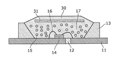
- a lead frame package is used as the package.
- the semiconductor light emitting device according to the present embodiment is a white LED light source that emits white light.
- the semiconductor light emitting device has a package made of resin having a recess, and includes a lead frame 11, an insulating resin layer 12, and a light reflecting resin layer 13.
- the lead frame 11 is exposed from the bottom surface of the recess of the package, and a light emitting diode (LED: Light Emitting Diode) is mounted on the lead frame 11 in the recess as the semiconductor light emitting element 14.
- the P electrode and N electrode of the semiconductor light emitting element 14 made of LED are electrically connected to the lead frame 11 by a gold wire 16.
- the resin layer 17 (first resin layer) made of transparent resin is filled in the package so as to enclose the semiconductor light emitting element 14.
- a region surrounded by the glass plate 18 that is a transparent substrate and the package is filled with the resin layer 17.
- the resin layer 17 is formed so as to contact the lead frame 11 in the recess of the package and cover the bottom surface of the recess. Ceramic fine particles 15 are dispersed in the resin layer 17.
- the quantum dot phosphor layer 19 (second resin layer) is a phosphor layer formed on the resin layer 17 and the semiconductor light emitting element 14.
- the quantum dot phosphor layer 19 is disposed in contact with the resin layer 17 filled in the package while being sealed by the glass plate 18.
- the quantum dot phosphor layer 19 includes semiconductor fine particles (quantum dot phosphor) having an excitation fluorescence spectrum that varies depending on the particle diameter, and a resin for dispersing and holding the semiconductor fine particles.
- the quantum dot phosphor layer 19 that is a phosphor layer is sealed in the glass plate 18 .
- the quantum dot phosphor layer 19 is dispersed in an acrylic resin and sandwiched between two glasses.
- the outer periphery of the glass plate 18 is sealed with an epoxy resin so that the acrylic resin does not directly touch the air.
- the resin material of the resin layer 17 in the present embodiment a silicone resin was used.
- the thermal conductivity of the silicone resin is as small as about 0.3 W / mK, and if it remains as it is, the quantum dot phosphor layer 19 cannot sufficiently dissipate heat. Efficiency will decrease. Therefore, in the present embodiment, the effective thermal conductivity of the resin layer 17 is increased by containing the ceramic fine particles 15 having good thermal conductivity in the silicone resin, and the temperature rise of the quantum dot phosphor layer 19 is suppressed. is doing.
- the resin layer 17 (first resin layer) contains the ceramic fine particles, so that the effective thermal conductivity of the resin layer 17 can be increased. it can.
- the heat dissipation of the quantum dot fluorescent substance layer 19 (2nd resin layer) can be improved, the temperature rise of the quantum dot fluorescent substance layer 19 can be suppressed. Therefore, it is possible to prevent the quantum dot phosphor (semiconductor fine particles) in the quantum dot phosphor layer 19 from deteriorating due to a temperature rise and reducing the light emission efficiency. Thereby, a highly efficient and highly reliable semiconductor light emitting device can be provided.
- the quantum dot phosphor layer 19 is enclosed in the glass plate 18. With this configuration, since the quantum dot phosphor in the quantum dot phosphor layer 19 does not come into contact with oxygen, deterioration of the quantum dot phosphor due to oxygen can be suppressed. Thereby, a highly reliable and high color rendering semiconductor light emitting device can be provided.
- AlN aluminum nitride
- AlN has a thermal conductivity of about 200 W / mK, which is about three orders of magnitude greater than that of silicone resin.
- AlN is transparent to light in the visible light region because the band gap is 6 eV or more. Therefore, it is preferable to use AlN fine particles as the ceramic fine particles 15.
- AlN may be pulverized into fine particles, mixed with a silicone resin, injected and filled into a package, and heated to 150 ° C. to be cured.
- AlN fine particles are contained in a silicone resin at a volume ratio of 10 vol%. In this case, the effective thermal conductivity of the silicone resin was 14.3 W / mK.
- AlN fine particles are used as the ceramic fine particles 15.
- a material that does not absorb light emitted from the semiconductor light emitting element 14 may be used as a material dispersed in the resin layer 17.
- SiO 2 , SiN, GaN Al 2 O 3 , TiO 2 , ZrO 2 , or ZnO 2 may be used.
- AlN and GaN have high thermal conductivity, the effective thermal conductivity of the silicone resin can be increased even when dispersed at a low concentration.
- a glass plate 18 having a quantum dot phosphor layer 19 is installed on the resin layer 17. At this time, it is preferable that the resin layer 17 and the glass plate 18 are brought into close contact with each other in order to increase the heat radiation sectional area.
- FIG. 2 is an assembly process diagram of the semiconductor light emitting device according to the first embodiment of the present invention.
- an LED is mounted as a semiconductor light emitting element 14 on a lead frame package including the lead frame 11.
- a wire bonding process is performed to connect the gold wire 16 to the semiconductor light emitting element 14.
- a silicone resin containing ceramic fine particles 15 is injected to form a resin layer 17.
- silicone resin is injected so as to rise slightly from the concave portion of the concave package.
- a defoaming process is performed to remove the gas remaining in the silicone resin.
- an LED into which a silicone resin has been injected is placed in a vacuum chamber connected to an oil rotary pump and left for 30 minutes.
- the glass plate 18 and the resin are pressed so as to press the resin layer 17 (silicone resin) raised by the glass plate 18 (glass plate) holding the quantum dot phosphor layer 19.
- the layer 17 is adhered.
- the resin layer 17 is pushed by the glass plate 18 and spreads laterally, and can be in contact with the glass plate 18 uniformly.
- the semiconductor light emitting device shown in FIG. 1 can be manufactured by thermosetting the silicone resin by heating.
- a phosphor layer in which a quantum dot phosphor layer is enclosed in a glass plate is used, but in a structure sandwiched between two glass plates, the quantum dot phosphor layer is thermally shielded by the glass plate. Therefore, heat radiation by the ceramic-containing resin layer is not sufficiently performed.
- the quantum dot phosphor is uniformly dispersed in the layer and the quantum dot phosphor layer and the ceramic-containing resin layer are in contact with each other.
- FIG. 3 is a schematic cross-sectional view of the semiconductor light-emitting device according to Embodiment 2 of the present invention.
- the quantum dot phosphor resin layer 22 (second resin layer) is a transparent substrate having an electrically conductive region by electrodeposition. It is formed on the surface and is arranged on the upper part of the package so as to face the semiconductor light emitting element 14.
- the inside of the package is filled with a resin layer 17 (first resin layer), and the resin layer 17 is sealed with a sealing member including the quantum dot phosphor resin layer 22.
- an ITO thin film is formed as a transparent electrode film 21 (electrically conductive region) on the surface of a transparent glass plate 20 (transparent substrate) as a sealing member for sealing the resin layer 17,
- a film in which a quantum dot phosphor resin layer 22 (second resin layer) is formed by using an electrodeposition method is used.
- the ITO thin film can be produced using a sputtering method.
- the sealing member configured as described above is arranged so that the quantum dot phosphor resin layer 22 is in contact with the resin layer 17 containing the ceramic fine particles 15.
- the quantum dot phosphor realizes uniform dispersion by being emulsified with a water-soluble or water-dispersible resin solvent.
- an epoxy resin is used as the electrodeposition resin.
- Epoxy resin is a material having oxygen permeability of 2 to 3 digits lower than that of silicone resin, and is one of resins that can be easily water-soluble or water-dispersible by amination.
- fluorine resins also have high oxygen barrier properties and high moisture resistance, and it is possible to suppress photooxidation reaction by dispersing quantum dot phosphors in these resins. .
- a water-soluble resin has an ionized or electrically polar part of the resin molecular skeleton in an aqueous solution, and the polar part and ionized region of the resin molecule are stabilized by hydration, so it is dissolved or dispersed in water to become an emulsion. can do.
- the quantum dot phosphor has a size of about 1 nm to 20 nm and the size equal to or smaller than that of the water-soluble resin molecule, so that it can be uniformly dispersed at a high concentration in the resin solution.
- the semiconductor fine particle according to the present invention is a quantum dot phosphor having a diameter of about 1 nm to 10 nm with InP as a nucleus, but the material of the phosphor does not have to be dissolved in water.
- a cadmium-based quantum dot phosphor Or chalcogenide fine particles may be used.
- quantum dot phosphors have a two-layer or three-layer structure called a core-shell structure for the purpose of improving luminous efficiency and reliability, but for efficient dispersion in water-soluble resin solvents.
- the chemical characteristics of the outermost layer of the quantum dot phosphor are important.
- the emulsification of the quantum dot phosphor is a result of the interaction with the alkyl main chain, and the outermost layer of the phosphor fine particles needs to be composed of a nonpolar or weakly polar ligand or layer. With this configuration, the quantum dot phosphor is trapped in the resin main chain by hydrophobic interaction.
- the quantum dot phosphor used in the present embodiment has a three-layer structure, the core is InP, and has a shell layer made of ZnS on the outside thereof.
- the outermost layer is provided with a ligand layer in which octane hydrocarbon is bonded as a ligand.
- the quantum dot phosphor resin layer 22 was formed using a cationic electrodeposition method.
- FIG. 4 is a schematic view for explaining the electrodeposition process.
- a cathode electrode 26 and an anode electrode 25 as a counter electrode are immersed in an epoxy resin solution 23 in which quantum dot phosphors 24 are dispersed.
- the epoxy resin is aminated (cationized), and the electrodeposition film 27 is formed on the object to be coated by using the object to be coated on the cathode electrode 26.
- the resin solvent is an acid solvent
- an anionic electrodeposition method is performed by using the article to be coated as an anode electrode.
- the electrodeposition film 27 (resin coating film) obtained by these methods is finally formed through a drying process and a curing process, and the quantum dot phosphor resin layer 22 is obtained.
- the electrodeposition method since a resin layer is formed only in a region to be energized, patterning of resin formation by electrodeposition is possible by protecting a desired position on the ITO film with an insulating resist.
- electrodeposition is performed by protecting with an resist so that an electrodeposition layer is not formed in a region where the outer peripheral portion of the package is in contact with the glass plate.
- an epoxy resin is used as the resin solution 23, but a fluorine-based resin may be used. Since these resins are resins excellent in oxygen resistance and moisture resistance, it is possible to effectively suppress deterioration of the quantum dot phosphor.
- the produced quantum dot phosphor resin layer 22 is disposed so as to be in contact with the resin layer 17 containing the ceramic fine particles 15 and is thermally cured by the same method as in the first embodiment.
- the effective thermal conductivity of the resin layer 17 is increased by containing ceramic fine particles as in the first embodiment. be able to.
- the heat dissipation of the quantum dot fluorescent resin layer 22 (2nd resin layer) can be improved, and the temperature rise of the quantum dot fluorescent resin layer 22 can be suppressed. Therefore, it is possible to prevent the quantum dot phosphor (semiconductor fine particles) in the quantum dot phosphor resin layer 22 from being deteriorated due to a temperature rise and the light emission efficiency being lowered.
- the quantum dot phosphor resin layer 22 is disposed so as to be in contact with the resin layer 17, so that the heat dissipation of the quantum dot phosphor resin layer 22 is further improved as compared with the first embodiment. Can be made.
- the quantum dot phosphor resin layer 22 is formed on the surface of the transparent substrate having the electrically conductive region by the electrodeposition method, the quantum dot phosphor is uniformly dispersed in the oxygen resistant resin. Can be made. Thereby, a highly reliable and high color rendering semiconductor light emitting device can be provided.
- the phosphor layers (quantum dot phosphor layer 19 and quantum dot phosphor resin layer 22) provided in contact with the resin layer 17 containing the ceramic fine particles 15 have a glass substrate. Although configured, a glass substrate is not necessarily required.
- Embodiment 3 a resin film containing a quantum dot phosphor is used as the phosphor layer without using a glass substrate.
- FIG. 5 is a schematic cross-sectional view of a semiconductor light emitting device according to Embodiment 3 of the present invention.
- the quantum dot phosphor film 31 is placed in a transparent resin layer 30 made of a silicone resin formed on the resin layer 17 (first resin layer). (Second resin layer) is provided.
- the quantum dot phosphor film 31 was produced by forming a resin layer containing the quantum dot phosphor on the flexible transparent conductive substrate by electrodeposition.
- the quantum dot phosphor film 31 may be attached by performing thermosetting of the silicone resin in a state where the quantum dot phosphor film 31 is placed on the upper part of the resin layer 17 made of silicone resin, but the adhesion between the quantum dot phosphor film 31 and the silicone resin. In order to further increase the thickness, it is preferable to embed the quantum dot phosphor film 31 in the resin layer.
- the quantum dot phosphor film 31 is disposed on the resin layer 17, and the resin layer 30 made of silicone resin is injected again from the top of the quantum dot phosphor film 31 and thermally cured. .
- the quantum dot phosphor film (resin film) is not peeled off, and a highly reliable semiconductor light emitting device can be provided.
- the ceramic fine particles are contained in the resin layer 17 (first resin layer) as in the first embodiment.
- Thermal conductivity can be increased.
- the heat dissipation of the quantum dot fluorescent film 31 (2nd resin layer) can be improved, the temperature rise of the quantum dot fluorescent film 31 can be suppressed. Therefore, it can suppress that the quantum dot fluorescent substance (semiconductor microparticles
- Resin containing ceramic fine particles has increased thermal conductivity, so heat generated by the phosphor layer due to Stokes loss can be dissipated.
- the phosphor layer is affected by self-heating caused by LED operation. It becomes easy to receive.
- the junction temperature may exceed 100 ° C., which may accelerate the deterioration of the phosphor layer.
- the LED does not include ceramic fine particles in order to dissipate the heat generated in the phosphor layer to the conductive region of the lead frame and at the same time prevent the heat generated by the LED from being transmitted to the phosphor layer.
- FIG. 6 is a schematic cross-sectional view of a semiconductor light emitting device according to Embodiment 4 of the present invention.
- a resin is further interposed between the resin layer 17 (first resin layer) and the semiconductor light emitting element 14.
- a layer 40 (third resin layer) is formed.
- the resin layer 40 is a transparent resin layer that does not contain ceramic fine particles and is composed only of a transparent resin made of a silicone resin or the like.
- the semiconductor light emitting element 14 is enclosed in the resin layer 40.
- the resin layer 40 does not contain ceramic fine particles and has a lower thermal conductivity than the resin layer 17. As a result, since the heat of the semiconductor light emitting element 14 is shielded by the resin layer 40, the heat of the semiconductor light emitting element 14 is transmitted to the quantum dot phosphor layer 19 even when the semiconductor light emitting element 14 is operated at a high output. Can be suppressed. Thereby, the resin layer 17 can effectively suppress the temperature rise of the quantum dot phosphor layer 19.
- the heat dissipation of the quantum dot phosphor layer 19 is improved by the resin layer 17 (first resin layer) containing ceramic fine particles.
- the heat of the semiconductor light emitting element 14 can be shielded by the resin layer 40 (third resin layer) that does not contain ceramic fine particles.
- the resin layer 17 containing the ceramic fine particles 15 is in contact with the conductive region of the lead frame in order to secure a route for dissipating heat generated by the Stokes loss of the quantum dot phosphor layer 19. It is preferable. With this configuration, both the heat radiation of the quantum dot phosphor layer 19 and the heat shielding of the semiconductor light emitting element 14 can be further achieved, so that the quantum dot phosphor layer 19 can be used even during high output operation of the semiconductor light emitting element 14. Thus, it is possible to provide a semiconductor light emitting device that can effectively suppress the temperature rise and has higher reliability.
- FIG. 7 is an assembly process diagram of the semiconductor light emitting device according to Embodiment 4 of the present invention.
- the semiconductor light emitting device 14 (LED) is mounted on the lead frame 11 and wire bonding is performed (FIG. 7A), and only the semiconductor light emitting device 14 encloses a transparent resin layer 40 made of silicone resin. As shown in FIG. 7B, partial injection is performed.
- the defoaming treatment of the silicone resin is performed in the state shown in FIG.
- a thermosetting treatment is performed at 150 ° C. for 30 minutes to shape the silicone resin (resin layer 40).
- the quantum dot phosphor layer 19 is encapsulated.
- the glass plate 18 thus pressed is pressed from above to thermally cure the resin layer 17.
- the quantum dot phosphor may be mixed in a high thermal conductive silicone resin containing ceramic fine particles. Therefore, since the heat of the quantum dot phosphor due to Stokes loss is dissipated to the adjacent ceramic fine particles, it is possible to suppress the temperature rise of the quantum dot phosphor.
- the silicone resin has high oxygen permeability, there is a concern that the quantum dot phosphor is deteriorated by photooxidation.
- Quantum dot phosphors often have low chemical stability due to their small particle size and a large proportion of atoms occupying the surface. Especially in excited fluorescence under high temperature environment, photooxidation of the surface of the quantum dot phosphor The reaction proceeds and may cause a sudden decrease in luminous efficiency.
- the quantum dot aggregated fine particles are formed by coating the surface of an aggregate of one or more quantum dot phosphors with a transparent resin or inorganic coating having oxygen barrier properties and moisture resistance.
- the quantum dot aggregate fine particles and ceramic fine particles are mixed in a silicone resin.
- FIG. 8 is a schematic cross-sectional view of a semiconductor light emitting device according to Embodiment 5 of the present invention.
- the resin layer 17 is configured such that quantum dot aggregated fine particles 60 that are phosphors that convert wavelengths and ceramic fine particles 15 are dispersed and held in a transparent resin such as a silicone resin.
- the quantum dot aggregate fine particle 60 is composed of an aggregate of one or more quantum dot phosphors.
- the surface of the aggregate is covered with a material having oxygen barrier properties and moisture resistance.
- the aggregate is covered with a transparent acrylic resin film.
- the semiconductor light emitting element 14 is tightly covered with a resin layer 17.
- an acrylic resin film is used as the film of the quantum dot aggregate fine particles 60, but a transparent inorganic film such as a transparent silicon oxide (SiO 2 ) may be used.
- a transparent inorganic film such as a transparent silicon oxide (SiO 2 ) may be used.
- the heat dissipation of the quantum dot phosphor layer 19 (second resin layer) is improved by the resin layer 17 (first resin layer) containing the ceramic fine particles 15.
- the deterioration of the quantum dot phosphor due to photo-oxidation can be suppressed by an acrylic resin film that coats the surface of the quantum dot phosphor.
- a semiconductor light emitting device can be provided.
- the light emitted from the LED has the highest luminance directly above the LED, and the luminance around the LED tends to decrease. Therefore, the phosphor layer is not uniformly irradiated, causing uneven emission.
- white fine particles that reflect visible light are used as the ceramic fine particles 15 in the semiconductor light emitting devices in the first to fifth embodiments.
- the white fine particles can be used as the ceramic fine particles 15 in the semiconductor light emitting devices in the first to fifth embodiments.
- titanium oxide (TiO 2 ) can be used as the white fine particles.
- the ceramic fine particles 15 do not absorb the emission wavelength of the LED and the fluorescence wavelength of the quantum dot phosphor, but depending on the size of the fine particles, the LED light may be strongly reflected. In order to reflect light from the LED efficiently, it is desirable that the particle diameter of the light scattering fine particles is as large as the wavelength of the light.
- the constituent material of the ceramic fine particles 15 is transparent to the light of the LED, but when the size of the fine particles is about the wavelength, a light scattering phenomenon called Mie scattering occurs. For this reason, even fine particles made of a transparent material are scattered in white.
- the particles become even smaller, they become dominated by light scattering called Rayleigh scattering, and the scattering intensity is proportional to the sixth power of the particle diameter. Therefore, if the particles are too small, the particles are again transparent to the LED light. It becomes.
- the size of about one-quarter to one wavelength of the wavelength is necessary, and the white LED has a visible light region of 400 nm to 700 nm. Is preferably 100 nm to 700 nm.
- a particle size of 100 nm to 450 nm is desirable.
- TiO 2 is used as the white fine particles.
- lead basic carbonate (2PbCO 3 .Pb (OH) 2 ) called lead white
- ZnO zinc white
- CaSO 4 .2H 2 O calcium sulfate hydrate
- the ceramic fine particles 15 are composed of the white fine particles, the light of the semiconductor light emitting element 14 (LED) is scattered by the white fine particles and uniformly in the phosphor layer. Is irradiated. Therefore, it is possible to provide a semiconductor light emitting device free from light unevenness. Also in the present embodiment, the heat generated in the phosphor layer can be dissipated as in the first to fifth embodiments. Therefore, in the present embodiment, a semiconductor light emitting device that can achieve both uniform light emission and high heat dissipation can be provided. Also in this embodiment, the effect in each embodiment can be achieved.
- diamond fine particles are used as the ceramic fine particles 15 in the semiconductor light emitting devices of the first to sixth embodiments.
- Diamond is transparent to visible light and has a very high thermal conductivity. Therefore, only by dispersing a small amount of diamond fine particles in the silicone resin, the thermal conductivity of the resin layer 17 is greatly increased, and the heat dissipation of the phosphor layer (quantum dot phosphor layer, etc.) is improved.
- diamond fine particles are formed by chemical vapor deposition.
- the thermal conductivity of the diamond fine particles was about 1200 W / mK.
- a thermal conductivity of about 15 W / mK which is the same as that of the silicone resin containing 10 vol% of AlN fine particles, was obtained. This is about 100 times the thermal conductivity of a silicone resin that does not contain ceramic fine particles.
- the semiconductor light emitting device by using the diamond fine particles, the phosphor layer can be radiated with high efficiency, so that the temperature rise of the quantum dot phosphor is effectively suppressed. It is possible to provide a semiconductor light emitting device with high efficiency, high reliability, and high color rendering. Also in this embodiment, the effect in each embodiment can be achieved.
- the ceramic fine particles 15 may be a rare earth phosphor that absorbs light emitted from the semiconductor light emitting element 14 (LED) and emits excitation light of the quantum dot phosphor as fluorescence.
- a silicon aluminum oxynitride (SiAlON: Eu) phosphor to which europium ions that are rare earth phosphors are added is used as the ceramic fine particles 15 in the semiconductor light emitting devices of the first to sixth embodiments.
- the phosphor layer (quantum dot phosphor layer 19 or the like) contained a red quantum dot phosphor having a particle diameter that gives red fluorescence.
- the semiconductor light emitting element 14 is an LED that emits blue light
- part of the blue light emitted by the semiconductor light emitting element 14 is absorbed by the SiAlON (Eu phosphor) and gives green fluorescence.
- the red quantum dot phosphor absorbs part of the green light emission and gives red fluorescence.
- the quantum dot phosphor converts the wavelength from green to red.
- the Stokes loss is smaller than in the case of wavelength conversion from blue to red, and the calorific value of the quantum dot phosphor is reduced. Therefore, since the temperature rise of the quantum dots can be further suppressed, a highly reliable semiconductor light emitting device can be provided.
- the wavelength of the light of the semiconductor light emitting element is converted by the ceramic fine particles, so that a semiconductor light emitting device with high color rendering properties and high reliability can be provided. Also in this embodiment, the effect in each embodiment can be achieved.
- the semiconductor light emitting device according to the present invention has been described above based on the embodiment, but the present invention is not limited to the above embodiment.
- the ceramic fine particles 15 may be transparent fine particles that transmit visible light. Thereby, since the light of the semiconductor light emitting element 14 is irradiated to the phosphor layer without loss, a highly efficient semiconductor light emitting device can be provided.
- the present invention can realize a semiconductor light emitting device with high reliability, high efficiency, and high color rendering, it is widely useful in white LED light sources such as display devices and lighting devices.
Abstract
The following are provided: a resin package that has a recess; a lead frame (11) exposed at the bottom of said recess; a semiconductor light-emitting element (14) mounted on said lead frame (11) inside the recess; a resin layer (17) formed so as to contact the lead frame (11) inside the recess and cover the bottom of the recess; and a quantum-dot phosphor layer (19) formed on top of the resin layer (17) and the semiconductor light-emitting element (14). The resin layer (17) contains ceramic microparticles (15), and the quantum-dot phosphor layer (19) contains the following: semiconductor microparticles with an excited fluorescence spectrum that varies with particle size; and a resin in which said semiconductor microparticles are held so as to form a dispersion.
Description
本発明は、半導体発光装置に関し、特に、量子ドット蛍光体を用いた半導体発光装置に関するものである。
The present invention relates to a semiconductor light emitting device, and more particularly to a semiconductor light emitting device using a quantum dot phosphor.
照明用、液晶ディスプレイバックライト用などの光源として高輝度白色LEDが用いられており、光源の高効率化および高演色性化の取り組みが行われている。白色LEDは、青色光を放射する半導体発光素子と緑、黄、赤色蛍光体などを組み合わせることで実現している。蛍光体の種類は、無機蛍光体、有機蛍光体、半導体から構成される量子ドット蛍光体がある。無機蛍光体を用いた白色LEDの例として、特許文献1のようなものがある。
High-brightness white LEDs are used as light sources for lighting and liquid crystal display backlights, and efforts are being made to improve the efficiency and color rendering of the light sources. The white LED is realized by combining a semiconductor light emitting element that emits blue light and green, yellow, and red phosphors. Types of phosphors include quantum dot phosphors composed of inorganic phosphors, organic phosphors, and semiconductors. There exists a thing like patent document 1 as an example of white LED using an inorganic fluorescent substance.
図9は、特許文献1に開示された従来の半導体発光装置を示す断面図である。
FIG. 9 is a cross-sectional view showing a conventional semiconductor light emitting device disclosed in Patent Document 1. In FIG.
図9に示すように、従来の半導体発光装置は、紫外線、青色光あるいは緑色光を放出する半導体発光素子1が、電気端子2、3が埋め込まれた容器8内に配置されたものであり、さらに、半導体発光素子1を埋めるように発光物質粒子6(無機の発光物質顔料)を含有する材料5が容器8内を覆っている。
As shown in FIG. 9, the conventional semiconductor light emitting device has a semiconductor light emitting element 1 that emits ultraviolet light, blue light, or green light disposed in a container 8 in which electrical terminals 2 and 3 are embedded, Further, a material 5 containing luminescent material particles 6 (inorganic luminescent material pigment) covers the inside of the container 8 so as to fill the semiconductor light emitting device 1.
LED光源は小型で省電力なため、ディスプレイデバイスや照明装置のキーデバイスとして用いられており、高輝度白色LEDの高効率化および高演色性化の取り組みが行われている。白色LEDは、青色LED光源と緑色蛍光体や黄色蛍光体との組み合わせが一般的であり、高効率・高演色性の実現には発光特性やエネルギー変換効率の優れた蛍光体が求められている。白色LEDに用いられる一般的な蛍光体は、希土類イオンを付活剤とした結晶微粒子であり、化学的に安定なものが多い。しかし、これらの蛍光体の光吸収効率は希土類の濃度に比例している一方で、濃度が高すぎると濃度消光によって発光効率の低下が生じるため、80%以上の高い量子効率を実現するのが困難であった。
Since the LED light source is small and power-saving, it is used as a key device for display devices and lighting devices, and efforts are being made to improve the efficiency and color rendering of high-intensity white LEDs. A white LED generally has a combination of a blue LED light source and a green phosphor or a yellow phosphor, and a phosphor with excellent light emission characteristics and energy conversion efficiency is required to achieve high efficiency and high color rendering. . Common phosphors used in white LEDs are fine crystal particles using rare earth ions as an activator, and many are chemically stable. However, while the light absorption efficiency of these phosphors is proportional to the concentration of rare earth, if the concentration is too high, the light emission efficiency is reduced by concentration quenching, so that a high quantum efficiency of 80% or more can be realized. It was difficult.
そこで、バンド端光吸収・発光を直接利用することで高い量子効率を実現する半導体蛍光微粒子が多数提案されており、特に量子ドット蛍光体と呼ばれる直径が数nmから数十nmの微粒子が、希土類を含まない新しい蛍光体材料として期待されている。量子ドット蛍光体は、量子サイズ効果によって同一材料の微粒子でも粒子径を制御することで可視光線領域において所望の波長帯の蛍光スペクトルを得ることが出来る。また、バンド端による光吸収・蛍光であるため、90%程度の高い外部量子効率を示すことから、高効率・高演色性を有する白色LEDを提供することができる。
Therefore, a large number of semiconductor fluorescent fine particles that realize high quantum efficiency by directly using band edge light absorption and emission have been proposed. Particularly, a fine particle called a quantum dot phosphor having a diameter of several nanometers to several tens of nanometers is rare earth. It is expected to be a new phosphor material that does not contain any material. The quantum dot phosphor can obtain a fluorescence spectrum in a desired wavelength band in the visible light region by controlling the particle diameter even with fine particles of the same material by the quantum size effect. Moreover, since it is light absorption and fluorescence by a band edge, since it shows high external quantum efficiency of about 90%, white LED which has high efficiency and high color rendering property can be provided.
また、この量子ドット蛍光体を用いて白色LED等の発光装置を構成する場合、特許文献1記載の容器8のような構成では注型エポキシ樹脂層の熱伝導率が小さいため、ヒートシンクとなるパッケージおよびフレーム樹脂層から離れた領域では、量子ドット蛍光体のストークスロスによる発熱によって樹脂層が高温化する。この結果、量子ドット蛍光体の温度が上昇して量子ドット蛍光体の劣化が生じて、発光効率が低下するという問題がある。
Further, when a light-emitting device such as a white LED is configured using this quantum dot phosphor, a package serving as a heat sink because the thermal conductivity of the cast epoxy resin layer is small in the configuration like the container 8 described in Patent Document 1. In the region away from the frame resin layer, the temperature of the resin layer rises due to heat generated by the Stokes loss of the quantum dot phosphor. As a result, there is a problem that the temperature of the quantum dot phosphor rises and the quantum dot phosphor is deteriorated, and the luminous efficiency is lowered.
本発明は、上記問題を解決するためになされたものであり、量子ドット蛍光体の温度上昇を抑制して発光効率の低下を抑えることができる半導体発光装置を提供することを目的とする。
The present invention has been made to solve the above-described problems, and an object of the present invention is to provide a semiconductor light-emitting device capable of suppressing a decrease in light emission efficiency by suppressing a temperature rise of a quantum dot phosphor.
上記目的を達成するために、本発明に係る第1の半導体発光装置の一態様は、凹部を有する樹脂からなるパッケージと、前記凹部の底面に露出したリードフレームと、前記凹部内のリードフレームに設置された半導体発光素子と、前記凹部内のリードフレームと接し底面を覆うように形成された第1の樹脂層と、前記第1の樹脂層および前記半導体発光素子の上に形成された第2の樹脂層とを備え、前記第1の樹脂層は、セラミックス微粒子を有し、前記第2の樹脂層は、粒子径によって異なる励起蛍光スペクトルを有する半導体微粒子と、前記半導体微粒子を分散保持する樹脂とを含むことを特徴とする。
In order to achieve the above object, one aspect of a first semiconductor light emitting device according to the present invention includes a package made of a resin having a recess, a lead frame exposed on a bottom surface of the recess, and a lead frame in the recess. A semiconductor light emitting element installed; a first resin layer formed to contact the lead frame in the recess and cover the bottom surface; and a second resin layer formed on the first resin layer and the semiconductor light emitting element. The first resin layer has ceramic fine particles, the second resin layer has semiconductor fine particles having an excitation fluorescence spectrum that varies depending on the particle diameter, and a resin for dispersing and holding the semiconductor fine particles. It is characterized by including.
この構成により、第1の樹脂層にセラミックス微粒子が含まれているので、第1の樹脂層の実効的な熱伝導率を増大させることができる。これにより、半導体微粒子を含む第2の樹脂層の放熱性を向上させることができるので、半導体微粒子の温度上昇を抑制することができる。従って、半導体微粒子が温度上昇によって劣化して発光効率が低下することを抑制することができる。これにより、高効率で高信頼性の半導体発光装置を提供できる。
With this configuration, since the first resin layer contains ceramic fine particles, the effective thermal conductivity of the first resin layer can be increased. Thereby, since the heat dissipation of the 2nd resin layer containing a semiconductor fine particle can be improved, the temperature rise of a semiconductor fine particle can be suppressed. Therefore, it can be suppressed that the semiconductor fine particles are deteriorated due to the temperature rise and the luminous efficiency is lowered. Thereby, a highly efficient and highly reliable semiconductor light emitting device can be provided.
さらに、本発明に係る第1の半導体発光装置の一態様において、前記第2の樹脂層は透明基板の中に封入されており、前記透明基板と前記パッケージとに囲まれた領域は、前記第1の樹脂層で充填されていることが好ましい。
Further, in one aspect of the first semiconductor light emitting device according to the present invention, the second resin layer is sealed in a transparent substrate, and the region surrounded by the transparent substrate and the package is the first substrate. It is preferable to be filled with one resin layer.
この構成により、半導体微粒子(量子ドット蛍光体)が酸素と触れないので、半導体微粒子の酸素による劣化を抑制することができる。これにより、高信頼性で高演色性の半導体発光装置を提供できる。
With this configuration, since the semiconductor fine particles (quantum dot phosphor) do not come into contact with oxygen, deterioration of the semiconductor fine particles due to oxygen can be suppressed. Thereby, a highly reliable and high color rendering semiconductor light emitting device can be provided.
さらに、本発明に係る第1の半導体発光装置の一態様において、前記第1の樹脂層と前記半導体発光素子との間にセラミックス微粒子を含まない第3の樹脂層を有することが好ましい。
Furthermore, in one aspect of the first semiconductor light emitting device according to the present invention, it is preferable that a third resin layer not containing ceramic fine particles is provided between the first resin layer and the semiconductor light emitting element.
この構成により、セラミックス微粒子を含まない熱伝導率の小さい第3の樹脂層によって半導体発光素子を熱的に遮蔽することができる。これにより、半導体微粒子(量子ドット蛍光体)の温度上昇を一層抑制することができるので、高輝度で高演色性の半導体発光装置を提供できる。
With this configuration, the semiconductor light-emitting element can be thermally shielded by the third resin layer that does not contain ceramic fine particles and has low thermal conductivity. Thereby, since the temperature rise of the semiconductor fine particles (quantum dot phosphor) can be further suppressed, a semiconductor light emitting device having high luminance and high color rendering can be provided.
さらに、本発明に係る第1の半導体発光装置の一態様において、前記第2の樹脂層は、電着法によって電気伝導性領域を有する透明基板表面に形成され、かつ、前記半導体発光素子と対向するように前記パッケージ上部に配置されており、前記パッケージの内側は、前記第1の樹脂層で充填されていることが好ましい。
Furthermore, in one aspect of the first semiconductor light emitting device according to the present invention, the second resin layer is formed on the surface of the transparent substrate having an electrically conductive region by an electrodeposition method, and faces the semiconductor light emitting element. As described above, it is preferably arranged on the upper part of the package, and the inside of the package is preferably filled with the first resin layer.
この構成により、耐酸素性樹脂に半導体微粒子(量子ドット蛍光体)を均一分散させることができる。これにより、高信頼性で高演色性の半導体発光装置を提供できる。
With this configuration, the semiconductor fine particles (quantum dot phosphor) can be uniformly dispersed in the oxygen-resistant resin. Thereby, a highly reliable and high color rendering semiconductor light emitting device can be provided.
また、本発明に係る第2の半導体発光装置の一態様は、パッケージ上に実装された半導体発光素子と波長を変換する蛍光体層と透明樹脂層からなる半導体発光装置であって、前記透明樹脂層はパッケージの排熱領域と接して半導体発光素子を封入しており、前記透明樹脂層はセラミックス微粒子を含有しており、前記蛍光体層は粒子径によって異なる励起蛍光スペクトルを有する半導体微粒子と前記半導体微粒子を分散保持する樹脂から構成されており、前記透明樹脂層の上部に接して設けられているものである。
Another aspect of the second semiconductor light emitting device according to the present invention is a semiconductor light emitting device comprising a semiconductor light emitting element mounted on a package, a phosphor layer for converting a wavelength, and a transparent resin layer, wherein the transparent resin The layer encloses the semiconductor light emitting element in contact with the exhaust heat region of the package, the transparent resin layer contains ceramic fine particles, and the phosphor layer includes the semiconductor fine particles having an excitation fluorescence spectrum that varies depending on the particle diameter, It is made of a resin for dispersing and holding semiconductor fine particles, and is provided in contact with the upper part of the transparent resin layer.
この構成であれば、熱伝導率の良いセラミックス微粒子を樹脂に分散させることから、熱電率の良い透明樹脂層を形成することができ、高出力励起光源を用いた場合においても、半導体微粒子(量子ドット蛍光体)を含有する蛍光体層から効率の良い放熱ができる。これにより、高輝度で高演色性の半導体発光装置を提供できる。
With this configuration, ceramic fine particles with good thermal conductivity are dispersed in the resin, so that a transparent resin layer with good thermoelectric conductivity can be formed. Even when a high-power excitation light source is used, semiconductor fine particles (quantum Efficient heat dissipation can be performed from the phosphor layer containing the dot phosphor. As a result, a semiconductor light emitting device having high luminance and high color rendering can be provided.
さらに、本発明に係る第2の半導体発光装置の一態様において、前記セラミックス微粒子を含有する透明樹脂と半導体発光素子との間にセラミックス微粒子を含まない第2の透明樹脂層を設けることが好ましい。
Furthermore, in one aspect of the second semiconductor light emitting device according to the present invention, it is preferable to provide a second transparent resin layer not containing ceramic fine particles between the transparent resin containing the ceramic fine particles and the semiconductor light emitting element.
この構成によれば、セラミックス微粒子を含まない熱伝導率の小さい第2の透明樹脂層によって半導体発光素子を熱的に遮蔽することができる。これにより、蛍光体層の温度上昇を抑制することができるので、高輝度で高演色性の半導体発光装置を提供できる。
According to this configuration, the semiconductor light emitting element can be thermally shielded by the second transparent resin layer having a small thermal conductivity and containing no ceramic fine particles. Thereby, since the temperature rise of a fluorescent substance layer can be suppressed, a high-intensity and high color rendering semiconductor light-emitting device can be provided.
さらに、本発明に係る第2の半導体発光装置の一態様において、前記蛍光体層が透明基板の中に封入されており、前記透明基板とパッケージに囲まれた領域は前記透明樹脂層で充填されていることが好ましい。
Furthermore, in one aspect of the second semiconductor light emitting device according to the present invention, the phosphor layer is sealed in a transparent substrate, and a region surrounded by the transparent substrate and the package is filled with the transparent resin layer. It is preferable.
この構成によれば、半導体微粒子(量子ドット蛍光体)が酸素と触れないので、半導体微粒子の酸素による劣化を抑制することができる。これにより、高信頼性で高演色性の半導体発光装置を提供できる。
According to this configuration, since the semiconductor fine particles (quantum dot phosphor) do not come into contact with oxygen, deterioration of the semiconductor fine particles due to oxygen can be suppressed. Thereby, a highly reliable and high color rendering semiconductor light emitting device can be provided.
さらに、本発明に係る第2の半導体発光装置の一態様において、前記蛍光体層は電着法によって電気伝導性領域を有する透明基板表面に形成されており、前記半導体発光素子と対向するようにパッケージ上部に配置されており、前記パッケージの内側は、前記セラミックス微粒子を含有する透明樹脂層で充填されていてもよい。
Furthermore, in one aspect of the second semiconductor light emitting device according to the present invention, the phosphor layer is formed on the surface of the transparent substrate having an electrically conductive region by an electrodeposition method so as to face the semiconductor light emitting element. It is arrange | positioned at the package upper part, The inside of the said package may be filled with the transparent resin layer containing the said ceramic fine particle.
この構成によれば、耐酸素性樹脂に半導体微粒子(量子ドット蛍光体)を均一分散させることが可能であることから、高信頼性で高演色性の半導体発光装置を提供できる。
According to this configuration, since the semiconductor fine particles (quantum dot phosphor) can be uniformly dispersed in the oxygen-resistant resin, a highly reliable and high color rendering semiconductor light emitting device can be provided.
さらに、本発明に係る第3の半導体発光装置の一態様は、凹部を有するパッケージと、前記パッケージに実装された半導体発光素子と、前記パッケージ内に形成され、波長を変換する蛍光体とセラミックス微粒子とが分散保持された樹脂層とを備え、前記蛍光体は、量子ドット蛍光体が1個または複数個集まった集合体からなり、前記集合体は、透明なアクリル樹脂膜またはシリコン酸化物によって被覆されており、前記半導体発光素子は、前記樹脂層によって被覆されていることを特徴とする。
Furthermore, one aspect of the third semiconductor light emitting device according to the present invention is a package having a recess, a semiconductor light emitting element mounted on the package, a phosphor formed in the package and converting a wavelength, and ceramic fine particles. The phosphor is composed of an aggregate of one or more quantum dot phosphors, and the aggregate is covered with a transparent acrylic resin film or silicon oxide. The semiconductor light emitting element is covered with the resin layer.
この構成によれば、セラミックス微粒子を含む熱伝導率の良い樹脂層に半導体微粒子(量子ドット蛍光体)が分散含有されることから、半導体微粒子の自己発熱を効率良く散逸させることができる。さらに、量子ドット蛍光体の表面がアクリル樹脂膜またはシリコン酸化物によって被膜されているので、量子ドット蛍光体の光酸化による劣化を抑制することができる。このように、本態様では、量子ドット蛍光体の温度上昇の抑制と量子ドット蛍光体の光酸化の抑制との両立を図ることができるので、高効率、高輝度で、高演色性の半導体発光装置を提供できる。
According to this configuration, since the semiconductor fine particles (quantum dot phosphor) are dispersedly contained in the resin layer containing ceramic fine particles and having high thermal conductivity, the self-heating of the semiconductor fine particles can be efficiently dissipated. Furthermore, since the surface of the quantum dot phosphor is coated with an acrylic resin film or silicon oxide, deterioration of the quantum dot phosphor due to photo-oxidation can be suppressed. As described above, in this aspect, since it is possible to achieve both suppression of the temperature rise of the quantum dot phosphor and suppression of photooxidation of the quantum dot phosphor, it is possible to achieve high efficiency, high luminance, and high color rendering semiconductor light emission. Equipment can be provided.
さらに、本発明に係る第1~第3の半導体発光装置の一態様において、前記セラミックス微粒子は可視光線を反射する白色微粒子であってもよい。
Furthermore, in one aspect of the first to third semiconductor light emitting devices according to the present invention, the ceramic fine particles may be white fine particles that reflect visible light.
この構成によれば、半導体発光素子から出射した光が蛍光体層(または、蛍光体や半導体微粒子を含む樹脂層)に均一に照射されるため、光ムラの無い半導体発光装置を提供できる。
According to this configuration, since the light emitted from the semiconductor light emitting element is uniformly applied to the phosphor layer (or the resin layer containing the phosphor and semiconductor fine particles), a semiconductor light emitting device free from light unevenness can be provided.
さらに、本発明に係る第1~第3の半導体発光装置の一態様において、前記セラミックス微粒子は可視光線を透過する透明微粒子であってもよい。
Furthermore, in one aspect of the first to third semiconductor light emitting devices according to the present invention, the ceramic fine particles may be transparent fine particles that transmit visible light.
この構成によれば、半導体発光素子の光は損失することなく蛍光体層(または、蛍光体や半導体微粒子を含む樹脂層)に照射されるため、高効率な半導体発光装置を提供できる。
According to this configuration, since the light of the semiconductor light emitting element is irradiated to the phosphor layer (or the resin layer containing the phosphor and semiconductor fine particles) without loss, a highly efficient semiconductor light emitting device can be provided.
さらに、本発明に係る第1~第3の半導体発光装置の一態様において、前記セラミックス微粒子はダイヤモンド微粒子であってもよい。
Furthermore, in one aspect of the first to third semiconductor light emitting devices according to the present invention, the ceramic fine particles may be diamond fine particles.
この構成によれば、熱伝導率が高いダイヤモンド微粒子によって蛍光体層(または、蛍光体や半導体微粒子を含む樹脂層)の温度上昇を抑制することができるので、高信頼性で高演色性の半導体発光装置を提供できる。
According to this configuration, since the temperature increase of the phosphor layer (or the resin layer containing the phosphor and semiconductor fine particles) can be suppressed by the diamond fine particles having high thermal conductivity, a highly reliable and high color rendering semiconductor. A light emitting device can be provided.
さらに、本発明に係る第1~第3の半導体発光装置の一態様において、前記セラミックス微粒子は、前記半導体発光素子の光を吸収し、前記蛍光体の励起光を蛍光として放射するものであってもよい。
Furthermore, in one aspect of the first to third semiconductor light emitting devices according to the present invention, the ceramic fine particles absorb light of the semiconductor light emitting element and emit excitation light of the phosphor as fluorescence. Also good.
この構成によれば、セラミックス微粒子によって半導体発光素子の光が波長変換されるので、高い演色性の半導体発光装置を提供できる。さらに、セラミックス微粒子によって半導体発光素子の光を波長変換することで半導体微粒子(蛍光体)のストークスロスが小さくなり自己発熱を抑制することが可能となることから、高信頼性の半導体発光装置を提供できる。
According to this configuration, the wavelength of the light of the semiconductor light emitting element is converted by the ceramic fine particles, so that a semiconductor light emitting device with high color rendering can be provided. Furthermore, by converting the wavelength of the light of the semiconductor light-emitting element with ceramic fine particles, the Stokes loss of the semiconductor fine particles (phosphor) can be reduced and self-heating can be suppressed, thereby providing a highly reliable semiconductor light-emitting device. it can.
さらに、本発明の半導体発光装置において、前記セラミックス微粒子の粒子直径が100nm以上700nm以下であることを特徴とする。
Furthermore, in the semiconductor light emitting device of the present invention, the ceramic fine particles have a particle diameter of 100 nm to 700 nm.
この構成であれば、可視光線を効率良く散乱させ、蛍光体に照射することができるため、高効率で高演色性の半導体発光装置を提供できる。
With this configuration, visible light can be efficiently scattered and irradiated onto the phosphor, so that a highly efficient and high color rendering semiconductor light emitting device can be provided.
本発明によれば、樹脂層にセラミックス微粒子が含まれているので、樹脂層の熱伝導率を大きくすることができる。これにより、蛍光体や半導体微粒子の自己発熱による温度上昇を抑制することできる。従って、高信頼性で高効率の半導体発光装置を提供することが出来る。
According to the present invention, since the ceramic fine particles are contained in the resin layer, the thermal conductivity of the resin layer can be increased. Thereby, the temperature rise by the self-heating of fluorescent substance or semiconductor fine particles can be suppressed. Therefore, a highly reliable and highly efficient semiconductor light emitting device can be provided.
以下、本発明に係る半導体発光装置について図面を参照しながら説明するが、本発明は、請求の範囲の記載に基づいて特定される。よって、以下の実施の形態における構成要素のうち、請求項に記載されていない構成要素は、本発明の課題を達成するのに必ずしも必要ではないが、より好ましい形態を構成するものとして説明される。また、各図において同じ構成要素には同じ符号を付している。なお、各図は、模式図であり、必ずしも厳密に図示したものではない。
Hereinafter, the semiconductor light emitting device according to the present invention will be described with reference to the drawings. However, the present invention is specified based on the description of the scope of claims. Therefore, among the constituent elements in the following embodiments, constituent elements that are not described in the claims are not necessarily required to achieve the object of the present invention, but are described as constituting more preferable embodiments. . Moreover, the same code | symbol is attached | subjected to the same component in each figure. Each figure is a schematic diagram and is not necessarily illustrated exactly.
(実施の形態1)
まず、本発明の実施の形態1に係る半導体発光装置について、図1を用いて説明する。 (Embodiment 1)
First, the semiconductor light emitting device according to the first embodiment of the present invention will be described with reference to FIG.
まず、本発明の実施の形態1に係る半導体発光装置について、図1を用いて説明する。 (Embodiment 1)
First, the semiconductor light emitting device according to the first embodiment of the present invention will be described with reference to FIG.
図1は、本発明の実施の形態1に係る半導体発光装置の断面概略図である。本実施の形態ではパッケージとしてリードフレームパッケージを用いている。また、本実施の形態に係る半導体発光装置は、白色光を放出する白色LED光源である。
FIG. 1 is a schematic cross-sectional view of a semiconductor light emitting device according to Embodiment 1 of the present invention. In this embodiment, a lead frame package is used as the package. Moreover, the semiconductor light emitting device according to the present embodiment is a white LED light source that emits white light.
図1に示すように、本発明の実施の形態1に係る半導体発光装置は、凹部を有する樹脂からなるパッケージを有し、リードフレーム11と絶縁樹脂層12と光反射樹脂層13とを備える。リードフレーム11はパッケージの凹部の底面から露出しており、凹部内のリードフレーム11上には半導体発光素子14として発光ダイオード(LED:Light Emitting Diode)が実装されている。LEDからなる半導体発光素子14のP電極およびN電極は、リードフレーム11に対して金ワイヤー16で電気的接点が取られている。
As shown in FIG. 1, the semiconductor light emitting device according to the first embodiment of the present invention has a package made of resin having a recess, and includes a lead frame 11, an insulating resin layer 12, and a light reflecting resin layer 13. The lead frame 11 is exposed from the bottom surface of the recess of the package, and a light emitting diode (LED: Light Emitting Diode) is mounted on the lead frame 11 in the recess as the semiconductor light emitting element 14. The P electrode and N electrode of the semiconductor light emitting element 14 made of LED are electrically connected to the lead frame 11 by a gold wire 16.
半導体発光素子14を封入する様に、パッケージ内には、透明樹脂からなる樹脂層17(第1の樹脂層)が充填されている。本実施の形態では、透明基板であるガラス板18とパッケージとに囲まれた領域が樹脂層17で充填されている。樹脂層17は、パッケージの凹部内のリードフレーム11と接し、凹部の底面を覆うように形成されている。樹脂層17中には、セラミックス微粒子15が分散されている。
The resin layer 17 (first resin layer) made of transparent resin is filled in the package so as to enclose the semiconductor light emitting element 14. In the present embodiment, a region surrounded by the glass plate 18 that is a transparent substrate and the package is filled with the resin layer 17. The resin layer 17 is formed so as to contact the lead frame 11 in the recess of the package and cover the bottom surface of the recess. Ceramic fine particles 15 are dispersed in the resin layer 17.
量子ドット蛍光体層19(第2の樹脂層)は、樹脂層17および半導体発光素子14の上に形成された蛍光体層である。本実施の形態において、量子ドット蛍光体層19は、ガラス板18に封止された状態で、パッケージ内に充填された樹脂層17に接して配置されている。量子ドット蛍光体層19は、粒子径によって異なる励起蛍光スペクトルを有する半導体微粒子(量子ドット蛍光体)と、半導体微粒子を分散保持する樹脂とを含む。
The quantum dot phosphor layer 19 (second resin layer) is a phosphor layer formed on the resin layer 17 and the semiconductor light emitting element 14. In the present embodiment, the quantum dot phosphor layer 19 is disposed in contact with the resin layer 17 filled in the package while being sealed by the glass plate 18. The quantum dot phosphor layer 19 includes semiconductor fine particles (quantum dot phosphor) having an excitation fluorescence spectrum that varies depending on the particle diameter, and a resin for dispersing and holding the semiconductor fine particles.
このように、本実施の形態では、蛍光体層である量子ドット蛍光体層19をガラス板18に封入したものを用いている。具体的には、量子ドット蛍光体層19をアクリル樹脂に分散させて2枚のガラスで挟んだ構造としている。ガラス板18の外周は、アクリル樹脂が直接空気に触れないようにエポキシ樹脂で封止されている。
Thus, in the present embodiment, a material in which the quantum dot phosphor layer 19 that is a phosphor layer is sealed in the glass plate 18 is used. Specifically, the quantum dot phosphor layer 19 is dispersed in an acrylic resin and sandwiched between two glasses. The outer periphery of the glass plate 18 is sealed with an epoxy resin so that the acrylic resin does not directly touch the air.
本実施の形態における樹脂層17の樹脂材料としてはシリコーン樹脂を用いた。シリコーン樹脂の熱伝導率は0.3W/mK程度と小さい値であり、このままでは、量子ドット蛍光体層19の十分な放熱ができないため、ストークスロスによる自己発熱によって量子ドット蛍光体が高温化し発光効率が低下してしまう。そこで、本実施の形態では、熱伝導率の良いセラミックス微粒子15をシリコーン樹脂に含有させることで、樹脂層17の実効的な熱伝導率を増大させ、量子ドット蛍光体層19の温度上昇を抑制している。
As the resin material of the resin layer 17 in the present embodiment, a silicone resin was used. The thermal conductivity of the silicone resin is as small as about 0.3 W / mK, and if it remains as it is, the quantum dot phosphor layer 19 cannot sufficiently dissipate heat. Efficiency will decrease. Therefore, in the present embodiment, the effective thermal conductivity of the resin layer 17 is increased by containing the ceramic fine particles 15 having good thermal conductivity in the silicone resin, and the temperature rise of the quantum dot phosphor layer 19 is suppressed. is doing.
以上、本実施の形態に係る半導体発光装置によれば、樹脂層17(第1の樹脂層)にセラミックス微粒子が含まれているので、樹脂層17の実効的な熱伝導率を増大させることができる。これにより、量子ドット蛍光体層19(第2の樹脂層)の放熱性を向上させることができるので、量子ドット蛍光体層19の温度上昇を抑制することができる。従って、量子ドット蛍光体層19内の量子ドット蛍光体(半導体微粒子)が温度上昇によって劣化して発光効率が低下することを抑制することができる。これにより、高効率で高信頼性の半導体発光装置を提供できる。
As described above, according to the semiconductor light emitting device according to the present embodiment, the resin layer 17 (first resin layer) contains the ceramic fine particles, so that the effective thermal conductivity of the resin layer 17 can be increased. it can. Thereby, since the heat dissipation of the quantum dot fluorescent substance layer 19 (2nd resin layer) can be improved, the temperature rise of the quantum dot fluorescent substance layer 19 can be suppressed. Therefore, it is possible to prevent the quantum dot phosphor (semiconductor fine particles) in the quantum dot phosphor layer 19 from deteriorating due to a temperature rise and reducing the light emission efficiency. Thereby, a highly efficient and highly reliable semiconductor light emitting device can be provided.
また、本実施の形態では、量子ドット蛍光体層19がガラス板18に封入されている。この構成により、量子ドット蛍光体層19内の量子ドット蛍光体が酸素と触れないので、量子ドット蛍光体の酸素による劣化を抑制することができる。これにより、高信頼性で高演色性の半導体発光装置を提供できる。
In this embodiment, the quantum dot phosphor layer 19 is enclosed in the glass plate 18. With this configuration, since the quantum dot phosphor in the quantum dot phosphor layer 19 does not come into contact with oxygen, deterioration of the quantum dot phosphor due to oxygen can be suppressed. Thereby, a highly reliable and high color rendering semiconductor light emitting device can be provided.
なお、本実施の形態において、セラミックス微粒子15としては窒化アルミニウム(AlN)を用いた。AlNは、熱伝導率が約200W/mKであり、シリコーン樹脂と比べて熱伝導率が約3桁も大きい。また、AlNは、バンドギャップが6eV以上であるため可視光線領域の光に対して透明である。従って、セラミックス微粒子15としてはAlN微粒子を用いること好ましい。セラミックス微粒子15としてAlNを用いる場合、例えば、AlNを粉砕して微粒子化し、シリコーン樹脂に混合した後、パッケージ内に注入充填し、150℃に加熱して硬化させればよい。また、本実施の形態では、AlN微粒子をシリコーン樹脂に体積比率10vol%で含有させた。この場合、シリコーン樹脂の実効的な熱伝導率は14.3W/mKとなった。
In this embodiment, aluminum nitride (AlN) is used as the ceramic fine particles 15. AlN has a thermal conductivity of about 200 W / mK, which is about three orders of magnitude greater than that of silicone resin. AlN is transparent to light in the visible light region because the band gap is 6 eV or more. Therefore, it is preferable to use AlN fine particles as the ceramic fine particles 15. When AlN is used as the ceramic fine particles 15, for example, AlN may be pulverized into fine particles, mixed with a silicone resin, injected and filled into a package, and heated to 150 ° C. to be cured. Further, in the present embodiment, AlN fine particles are contained in a silicone resin at a volume ratio of 10 vol%. In this case, the effective thermal conductivity of the silicone resin was 14.3 W / mK.
また、本実施の形態では、セラミックス微粒子15としてAlN微粒子を用いたが、樹脂層17に分散させる材料としては半導体発光素子14の発光を吸収しない材料を用いればよく、例えばSiO2、SiN、GaN、Al2O3、TiO2、ZrO2、または、ZnO2などでも良い。特にAlNやGaNは熱伝導率が高いため低濃度に分散させた場合であってもシリコーン樹脂の実効的な熱伝導率を増大させることが可能である。
In the present embodiment, AlN fine particles are used as the ceramic fine particles 15. However, a material that does not absorb light emitted from the semiconductor light emitting element 14 may be used as a material dispersed in the resin layer 17. For example, SiO 2 , SiN, GaN Al 2 O 3 , TiO 2 , ZrO 2 , or ZnO 2 may be used. In particular, since AlN and GaN have high thermal conductivity, the effective thermal conductivity of the silicone resin can be increased even when dispersed at a low concentration.
また、本実施の形態では、樹脂層17の上部に、量子ドット蛍光体層19を有するガラス板18を設置している。このとき、放熱断面積を大きくするために、樹脂層17とガラス板18とを密着させることが好ましい。
Further, in the present embodiment, a glass plate 18 having a quantum dot phosphor layer 19 is installed on the resin layer 17. At this time, it is preferable that the resin layer 17 and the glass plate 18 are brought into close contact with each other in order to increase the heat radiation sectional area.
次に、本発明の実施の形態1に係る半導体発光装置の製造方法(組み立て方法)について、図2を用いて説明する。図2は、本発明の実施の形態1に係る半導体発光装置の組み立て工程図である。
Next, a manufacturing method (assembly method) of the semiconductor light emitting device according to Embodiment 1 of the present invention will be described with reference to FIG. FIG. 2 is an assembly process diagram of the semiconductor light emitting device according to the first embodiment of the present invention.
まず、図2(a)に示すように、リードフレーム11からなるリードフレームパッケージ上に、半導体発光素子14としてLEDを実装する。
First, as shown in FIG. 2A, an LED is mounted as a semiconductor light emitting element 14 on a lead frame package including the lead frame 11.
その後、図2(b)に示すように、ワイヤーボンディング工程を行って、半導体発光素子14に金ワイヤー16を接続する。
Thereafter, as shown in FIG. 2B, a wire bonding process is performed to connect the gold wire 16 to the semiconductor light emitting element 14.
その後、図2(c)に示すように、セラミックス微粒子15を含有したシリコーン樹脂を注入して樹脂層17を形成する。このとき、凹型パッケージの凹部から少し盛り上がるようにシリコーン樹脂を注入する。
Thereafter, as shown in FIG. 2C, a silicone resin containing ceramic fine particles 15 is injected to form a resin layer 17. At this time, silicone resin is injected so as to rise slightly from the concave portion of the concave package.
次に、図示しないが、シリコーン樹脂中に残存する気体を除去する脱泡処理を行う。本実施の形態では、油回転ポンプに接続した真空室内に、シリコーン樹脂を注入したLEDを入れて30分放置した。
Next, although not shown, a defoaming process is performed to remove the gas remaining in the silicone resin. In this embodiment, an LED into which a silicone resin has been injected is placed in a vacuum chamber connected to an oil rotary pump and left for 30 minutes.
次に、図2(d)に示すように、量子ドット蛍光体層19を保持したガラス板18(ガラスプレート)によって盛り上がった樹脂層17(シリコーン樹脂)を押さえ付けるように、ガラス板18と樹脂層17とを接着させる。このようにすることで、樹脂層17は、ガラス板18に押されて横に広がると共に、均一にガラス板18と接することができる。
Next, as shown in FIG. 2D, the glass plate 18 and the resin are pressed so as to press the resin layer 17 (silicone resin) raised by the glass plate 18 (glass plate) holding the quantum dot phosphor layer 19. The layer 17 is adhered. By doing in this way, the resin layer 17 is pushed by the glass plate 18 and spreads laterally, and can be in contact with the glass plate 18 uniformly.
最後に、図示しないが、加熱することによってシリコーン樹脂を熱硬化させることで、図1に示す半導体発光装置を製造することができる。
Finally, although not shown, the semiconductor light emitting device shown in FIG. 1 can be manufactured by thermosetting the silicone resin by heating.
(実施の形態2)
次に、本発明の実施の形態2に係る半導体発光装置について説明する。 (Embodiment 2)
Next, a semiconductor light emitting device according to the second embodiment of the present invention will be described.
次に、本発明の実施の形態2に係る半導体発光装置について説明する。 (Embodiment 2)
Next, a semiconductor light emitting device according to the second embodiment of the present invention will be described.
実施の形態1では蛍光体層として量子ドット蛍光体層をガラス板に封入したものを用いたが、2枚のガラス板で挟み込んだ構造では、量子ドット蛍光体層がガラス板によって熱的に遮蔽されることから、セラミックス含有樹脂層による放熱が十分になされない。
In the first embodiment, a phosphor layer in which a quantum dot phosphor layer is enclosed in a glass plate is used, but in a structure sandwiched between two glass plates, the quantum dot phosphor layer is thermally shielded by the glass plate. Therefore, heat radiation by the ceramic-containing resin layer is not sufficiently performed.
また、量子ドット蛍光体層をガラス板に封入した構造の場合、ガラス封止の機密性を十分に確保することが困難であったり、量子ドット蛍光体層内における量子ドット蛍光体の均一な分散が困難であったりなど、別の課題もある。
In addition, in the case of a structure in which the quantum dot phosphor layer is enclosed in a glass plate, it is difficult to ensure sufficient confidentiality of the glass seal, or the quantum dot phosphor layer is uniformly dispersed in the quantum dot phosphor layer. There are other issues, such as being difficult.
そこで、量子ドット蛍光体を層内に均一に分散させ、かつ量子ドット蛍光体層とセラミックス含有樹脂層とが接する構成とすることが好ましい。
Therefore, it is preferable that the quantum dot phosphor is uniformly dispersed in the layer and the quantum dot phosphor layer and the ceramic-containing resin layer are in contact with each other.
図3は、本発明の実施の形態2に係る半導体発光装置の断面概略図である。
FIG. 3 is a schematic cross-sectional view of the semiconductor light-emitting device according to Embodiment 2 of the present invention.
図3に示すように、本発明の実施の形態2に係る半導体発光装置では、量子ドット蛍光体樹脂層22(第2の樹脂層)が、電着法によって電気伝導性領域を有する透明基板の表面に形成されており、かつ、半導体発光素子14と対向するようにパッケージ上部に配置されている。また、パッケージの内側は樹脂層17(第1の樹脂層)で充填されており、樹脂層17は、量子ドット蛍光体樹脂層22を含む封止部材によって封止されている。
As shown in FIG. 3, in the semiconductor light emitting device according to Embodiment 2 of the present invention, the quantum dot phosphor resin layer 22 (second resin layer) is a transparent substrate having an electrically conductive region by electrodeposition. It is formed on the surface and is arranged on the upper part of the package so as to face the semiconductor light emitting element 14. The inside of the package is filled with a resin layer 17 (first resin layer), and the resin layer 17 is sealed with a sealing member including the quantum dot phosphor resin layer 22.
本実施の形態では、樹脂層17を封止する封止部材として、透明なガラス板20(透明基板)の表面上に透明電極膜21(電気伝導性領域)としてITO薄膜を形成し、その上部に電着法を用いて量子ドット蛍光体樹脂層22(第2の樹脂層)を成膜したものを用いている。ITO薄膜は、スパッタ法を用いて作製することができる。このように構成された封止部材は、量子ドット蛍光体樹脂層22がセラミックス微粒子15を含有する樹脂層17に接するように配置されている。
In the present embodiment, an ITO thin film is formed as a transparent electrode film 21 (electrically conductive region) on the surface of a transparent glass plate 20 (transparent substrate) as a sealing member for sealing the resin layer 17, In addition, a film in which a quantum dot phosphor resin layer 22 (second resin layer) is formed by using an electrodeposition method is used. The ITO thin film can be produced using a sputtering method. The sealing member configured as described above is arranged so that the quantum dot phosphor resin layer 22 is in contact with the resin layer 17 containing the ceramic fine particles 15.
ここで、蛍光体層として機能する量子ドット蛍光体樹脂層22の製造方法について説明する。量子ドット蛍光体は、水溶性または水分散性樹脂溶剤とエマルジョン化させることで均一な分散を実現する。本実施の形態では、電着樹脂としてエポキシ系樹脂を用いた。エポキシ系樹脂はシリコーン樹脂に比べると酸素透過性が2桁から3桁ほど低い材料であり、アミン化することで水溶性化または水分散性化が容易な樹脂の一つである。また、エポキシ系樹脂以外にもフッ素系樹脂も高い酸素バリア性および高い耐湿性を有しており、量子ドット蛍光体をこれらの樹脂に分散させることで光酸化反応を抑制することが可能である。水溶性樹脂は水溶液中で樹脂分子骨格の一部がイオン化または電気的極性を有しており、樹脂分子の極性箇所やイオン化領域が水和によって安定化するため水に溶解または分散してエマルジョン化することができる。このとき蛍光体微粒子のサイズが大きいと、樹脂分子による捕捉が十分行われず、沈降・沈殿が生じてしまう。一方、量子ドット蛍光体は1nm~20nm程度であり水溶性樹脂分子と同等、またはそれ以下のサイズであるため、樹脂溶液へ均一にかつ高濃度で分散させることが可能となる。
Here, a manufacturing method of the quantum dot phosphor resin layer 22 that functions as a phosphor layer will be described. The quantum dot phosphor realizes uniform dispersion by being emulsified with a water-soluble or water-dispersible resin solvent. In the present embodiment, an epoxy resin is used as the electrodeposition resin. Epoxy resin is a material having oxygen permeability of 2 to 3 digits lower than that of silicone resin, and is one of resins that can be easily water-soluble or water-dispersible by amination. In addition to epoxy resins, fluorine resins also have high oxygen barrier properties and high moisture resistance, and it is possible to suppress photooxidation reaction by dispersing quantum dot phosphors in these resins. . A water-soluble resin has an ionized or electrically polar part of the resin molecular skeleton in an aqueous solution, and the polar part and ionized region of the resin molecule are stabilized by hydration, so it is dissolved or dispersed in water to become an emulsion. can do. At this time, if the size of the phosphor fine particles is large, the capture by the resin molecules is not sufficiently performed, and sedimentation / precipitation occurs. On the other hand, the quantum dot phosphor has a size of about 1 nm to 20 nm and the size equal to or smaller than that of the water-soluble resin molecule, so that it can be uniformly dispersed at a high concentration in the resin solution.
本発明に係る半導体微粒子は、InPを核とする直径1nmから10nm程度の量子ドット蛍光体であるが、蛍光体の材料は水に溶解しなければよく、InP以外にもカドミウム系量子ドット蛍光体やカルコゲナイド系微粒子などでも良い。
The semiconductor fine particle according to the present invention is a quantum dot phosphor having a diameter of about 1 nm to 10 nm with InP as a nucleus, but the material of the phosphor does not have to be dissolved in water. In addition to InP, a cadmium-based quantum dot phosphor Or chalcogenide fine particles may be used.
量子ドット蛍光体の多くは、発光効率の向上や信頼性向上を目的としたコア-シェル構造と呼ばれる2層または3層構造を有しているが、水溶性樹脂溶剤へ効率良く分散をさせるためには、量子ドット蛍光体の最外層の化学的特性が重要となる。量子ドット蛍光体のエマルジョン化はアルキル主鎖との相互作用の結果であり、蛍光体微粒子の最外層は無極性や極性の弱い配位子や層から構成されることが必要となる。この構成によって量子ドット蛍光体は疎水性相互作用により樹脂主鎖に捕捉される。
Many of the quantum dot phosphors have a two-layer or three-layer structure called a core-shell structure for the purpose of improving luminous efficiency and reliability, but for efficient dispersion in water-soluble resin solvents. For this, the chemical characteristics of the outermost layer of the quantum dot phosphor are important. The emulsification of the quantum dot phosphor is a result of the interaction with the alkyl main chain, and the outermost layer of the phosphor fine particles needs to be composed of a nonpolar or weakly polar ligand or layer. With this configuration, the quantum dot phosphor is trapped in the resin main chain by hydrophobic interaction.
なお、本実施の形態で用いた量子ドット蛍光体は、3層構造であり、コアはInPであり、その外側にZnSから成るシェル層を有している。最外層は、オクタン系の炭化水素を配位子として結合させたリガンド層を設けている。最外層に疎水性の強い炭化水素からなるリガンド層を設けることで、水溶液中で効率良く量子ドット蛍光体が樹脂分子の主鎖に捕捉される。その結果、高濃度で高均一に量子ドットをエマルジョン化させることが可能となる。樹脂溶剤との分散性を高める上では、分子量が小さいほうが好ましい。具体的には、室温で液体として存在することが出来ることが必要であるため、炭素数が15個以下でなければならない。
The quantum dot phosphor used in the present embodiment has a three-layer structure, the core is InP, and has a shell layer made of ZnS on the outside thereof. The outermost layer is provided with a ligand layer in which octane hydrocarbon is bonded as a ligand. By providing a ligand layer made of a highly hydrophobic hydrocarbon in the outermost layer, the quantum dot phosphor is efficiently trapped in the main chain of the resin molecule in an aqueous solution. As a result, it is possible to emulsify the quantum dots with high concentration and high uniformity. In order to improve the dispersibility with the resin solvent, a smaller molecular weight is preferable. Specifically, since it is necessary to be able to exist as a liquid at room temperature, the number of carbons must be 15 or less.
本実施の形態において、量子ドット蛍光体樹脂層22は、カチオン電着法を用いて形成した。図4は、その電着工程を説明するための概略図である。
In the present embodiment, the quantum dot phosphor resin layer 22 was formed using a cationic electrodeposition method. FIG. 4 is a schematic view for explaining the electrodeposition process.
図4に示すように、量子ドット蛍光体24を分散させたエポキシ系の樹脂溶液23にカソード電極26と対向電極であるアノード電極25とを浸す。エポキシ系樹脂はアミン化(陽イオン化)しており、カソード電極26に被塗物を用いることで電着膜27が被塗物上に成膜される。一方、樹脂溶剤が酸系であれば、被塗物をアノード電極とすることでアニオン型電着法となる。これらの方法で得られた電着膜27(樹脂塗膜)は、乾燥工程および硬化工程を経て最終形成され、量子ドット蛍光体樹脂層22が得られる。電着法では、通電する領域のみ樹脂層が形成されることから、ITO膜上の所望の位置を絶縁性レジストで保護することで、電着による樹脂形成のパターニングが可能である。
As shown in FIG. 4, a cathode electrode 26 and an anode electrode 25 as a counter electrode are immersed in an epoxy resin solution 23 in which quantum dot phosphors 24 are dispersed. The epoxy resin is aminated (cationized), and the electrodeposition film 27 is formed on the object to be coated by using the object to be coated on the cathode electrode 26. On the other hand, if the resin solvent is an acid solvent, an anionic electrodeposition method is performed by using the article to be coated as an anode electrode. The electrodeposition film 27 (resin coating film) obtained by these methods is finally formed through a drying process and a curing process, and the quantum dot phosphor resin layer 22 is obtained. In the electrodeposition method, since a resin layer is formed only in a region to be energized, patterning of resin formation by electrodeposition is possible by protecting a desired position on the ITO film with an insulating resist.
なお、本実施の形態では、パッケージの外周部分とガラス板とが接する領域には電着層を形成させないようにレジストで保護して電着を行った。また、本実施の形態では樹脂溶液23としてエポキシ樹脂を用いたが、フッ素系樹脂を用いてもよい。これらの樹脂は、耐酸素性および耐湿性に優れた樹脂であることから、量子ドット蛍光体の劣化を効果的に抑制することが可能となる。また、作製した量子ドット蛍光体樹脂層22は、セラミックス微粒子15を含有する樹脂層17と接するように配置し、実施の形態1と同様の方法で熱硬化させる。
In this embodiment, electrodeposition is performed by protecting with an resist so that an electrodeposition layer is not formed in a region where the outer peripheral portion of the package is in contact with the glass plate. In this embodiment, an epoxy resin is used as the resin solution 23, but a fluorine-based resin may be used. Since these resins are resins excellent in oxygen resistance and moisture resistance, it is possible to effectively suppress deterioration of the quantum dot phosphor. Further, the produced quantum dot phosphor resin layer 22 is disposed so as to be in contact with the resin layer 17 containing the ceramic fine particles 15 and is thermally cured by the same method as in the first embodiment.
以上、本実施の形態に係る半導体発光装置によれば、実施の形態1と同様に、セラミックス微粒子を含有させることで樹脂層17(第1の樹脂層)の実効的な熱伝導率を増大させることができる。これにより、量子ドット蛍光体樹脂層22(第2の樹脂層)の放熱性を向上させることができ、量子ドット蛍光体樹脂層22の温度上昇を抑制することができる。従って、量子ドット蛍光体樹脂層22内の量子ドット蛍光体(半導体微粒子)が温度上昇によって劣化して発光効率が低下することを抑制することができる。
As described above, according to the semiconductor light emitting device according to the present embodiment, the effective thermal conductivity of the resin layer 17 (first resin layer) is increased by containing ceramic fine particles as in the first embodiment. be able to. Thereby, the heat dissipation of the quantum dot fluorescent resin layer 22 (2nd resin layer) can be improved, and the temperature rise of the quantum dot fluorescent resin layer 22 can be suppressed. Therefore, it is possible to prevent the quantum dot phosphor (semiconductor fine particles) in the quantum dot phosphor resin layer 22 from being deteriorated due to a temperature rise and the light emission efficiency being lowered.
しかも、本実施の形態では、量子ドット蛍光体樹脂層22が樹脂層17に接するように配置されているので、実施の形態1と比べて、量子ドット蛍光体樹脂層22の放熱性をさらに向上させることができる。
In addition, in the present embodiment, the quantum dot phosphor resin layer 22 is disposed so as to be in contact with the resin layer 17, so that the heat dissipation of the quantum dot phosphor resin layer 22 is further improved as compared with the first embodiment. Can be made.
また、本実施の形態では、量子ドット蛍光体樹脂層22が、電着法によって電気伝導性領域を有する透明基板の表面に形成されているので、耐酸素性樹脂に量子ドット蛍光体を均一に分散させることができる。これにより、高信頼性で高演色性の半導体発光装置を提供できる。
In the present embodiment, since the quantum dot phosphor resin layer 22 is formed on the surface of the transparent substrate having the electrically conductive region by the electrodeposition method, the quantum dot phosphor is uniformly dispersed in the oxygen resistant resin. Can be made. Thereby, a highly reliable and high color rendering semiconductor light emitting device can be provided.
(実施の形態3)
次に、本発明の実施の形態3に係る半導体発光装置について説明する。 (Embodiment 3)
Next, a semiconductor light emitting device according to the third embodiment of the present invention will be described.
次に、本発明の実施の形態3に係る半導体発光装置について説明する。 (Embodiment 3)
Next, a semiconductor light emitting device according to the third embodiment of the present invention will be described.
実施の形態1、2では、セラミックス微粒子15が含有された樹脂層17に接して設けられる蛍光体層(量子ドット蛍光体層19、量子ドット蛍光体樹脂層22)は、ガラス基板を有するように構成されていたが、ガラス基板は必ずしも必要ではない。
In the first and second embodiments, the phosphor layers (quantum dot phosphor layer 19 and quantum dot phosphor resin layer 22) provided in contact with the resin layer 17 containing the ceramic fine particles 15 have a glass substrate. Although configured, a glass substrate is not necessarily required.
そこで、実施の形態3では、ガラス基板を用いずに、蛍光体層として、量子ドット蛍光体を含有した樹脂フィルムを用いている。
Therefore, in Embodiment 3, a resin film containing a quantum dot phosphor is used as the phosphor layer without using a glass substrate.
図5は、本発明の実施の形態3に係る半導体発光装置の断面概略図である。
FIG. 5 is a schematic cross-sectional view of a semiconductor light emitting device according to Embodiment 3 of the present invention.
図5に示すように、本実施の形態に係る半導体発光装置では、樹脂層17(第1の樹脂層)の上に形成したシリコーン樹脂からなる透明な樹脂層30内に量子ドット蛍光体フィルム31(第2の樹脂層)を設けている。量子ドット蛍光体フィルム31は、フレキシブル透明導電性基板上に電着法によって量子ドット蛍光体を含有した樹脂層を形成することで作製した。
As shown in FIG. 5, in the semiconductor light emitting device according to the present embodiment, the quantum dot phosphor film 31 is placed in a transparent resin layer 30 made of a silicone resin formed on the resin layer 17 (first resin layer). (Second resin layer) is provided. The quantum dot phosphor film 31 was produced by forming a resin layer containing the quantum dot phosphor on the flexible transparent conductive substrate by electrodeposition.
量子ドット蛍光体フィルム31は、シリコーン樹脂からなる樹脂層17の上部に乗せた状態でシリコーン樹脂の熱硬化を行うことで取り付けても良いが、量子ドット蛍光体フィルム31とシリコーン樹脂との密着性をより高めるためには、量子ドット蛍光体フィルム31を樹脂層の内部に埋め込むほうが好ましい。
The quantum dot phosphor film 31 may be attached by performing thermosetting of the silicone resin in a state where the quantum dot phosphor film 31 is placed on the upper part of the resin layer 17 made of silicone resin, but the adhesion between the quantum dot phosphor film 31 and the silicone resin. In order to further increase the thickness, it is preferable to embed the quantum dot phosphor film 31 in the resin layer.
そこで、本実施の形態では、量子ドット蛍光体フィルム31を樹脂層17の上に配置して、量子ドット蛍光体フィルム31の上部から再度シリコーン樹脂からなる樹脂層30を注入し熱硬化している。この構成であれば、量子ドット蛍光体フィルム(樹脂フィルム)が剥がれる事はなく、高い信頼性を有する半導体発光装置を提供できる。
Therefore, in the present embodiment, the quantum dot phosphor film 31 is disposed on the resin layer 17, and the resin layer 30 made of silicone resin is injected again from the top of the quantum dot phosphor film 31 and thermally cured. . With this configuration, the quantum dot phosphor film (resin film) is not peeled off, and a highly reliable semiconductor light emitting device can be provided.
以上、本実施の形態に係る半導体発光装置によれば、実施の形態1と同様に、樹脂層17(第1の樹脂層)にセラミックス微粒子が含まれているので、樹脂層17の実効的な熱伝導率を増大させることができる。これにより、量子ドット蛍光体フィルム31(第2の樹脂層)の放熱性を向上させることができるので、量子ドット蛍光体フィルム31の温度上昇を抑制することができる。従って、量子ドット蛍光体フィルム31内の量子ドット蛍光体(半導体微粒子)が温度上昇によって劣化して発光効率が低下することを抑制することができる。
As described above, according to the semiconductor light emitting device according to the present embodiment, the ceramic fine particles are contained in the resin layer 17 (first resin layer) as in the first embodiment. Thermal conductivity can be increased. Thereby, since the heat dissipation of the quantum dot fluorescent film 31 (2nd resin layer) can be improved, the temperature rise of the quantum dot fluorescent film 31 can be suppressed. Therefore, it can suppress that the quantum dot fluorescent substance (semiconductor microparticles | fine-particles) in the quantum dot fluorescent substance film 31 deteriorates by a temperature rise, and luminous efficiency falls.
(実施の形態4)
次に、本発明の実施の形態4に係る半導体発光装置について説明する。 (Embodiment 4)
Next, a semiconductor light-emitting device according to Embodiment 4 of the present invention will be described.
次に、本発明の実施の形態4に係る半導体発光装置について説明する。 (Embodiment 4)
Next, a semiconductor light-emitting device according to Embodiment 4 of the present invention will be described.
セラミックス微粒子を含有した樹脂は熱伝導率が増大するため、ストークスロスによる蛍光体層の発熱を放熱させることが出来る一方、熱が伝わりやすいために蛍光体層はLEDの動作に伴う自己発熱の影響を受けやすくなる。特にLEDを高出力動作させる場合、その接合温度は100度を超える場合もあるため、蛍光体層の劣化を加速させる恐れがある。
Resin containing ceramic fine particles has increased thermal conductivity, so heat generated by the phosphor layer due to Stokes loss can be dissipated. However, since the heat is easily transmitted, the phosphor layer is affected by self-heating caused by LED operation. It becomes easy to receive. In particular, when the LED is operated at a high output, the junction temperature may exceed 100 ° C., which may accelerate the deterioration of the phosphor layer.
そこで、実施の形態4では、蛍光体層の発熱をリードフレームの導電性領域に放熱させると同時に、LEDの発熱が蛍光体層に伝わらないようにするために、LEDを、セラミックス微粒子を含まない樹脂層によって封入した。
Therefore, in the fourth embodiment, the LED does not include ceramic fine particles in order to dissipate the heat generated in the phosphor layer to the conductive region of the lead frame and at the same time prevent the heat generated by the LED from being transmitted to the phosphor layer. Encapsulated by a resin layer.
図6は、本発明の実施の形態4に係る半導体発光装置の断面概略図である。
FIG. 6 is a schematic cross-sectional view of a semiconductor light emitting device according to Embodiment 4 of the present invention.
図6に示すように、本実施の形態に係る半導体発光装置では、実施の形態1における半導体発光装置において、さらに、樹脂層17(第1の樹脂層)と半導体発光素子14との間に樹脂層40(第3の樹脂層)が形成されている。樹脂層40は、セラミックス微粒子が含まれておらず、シリコーン樹脂等からなる透明樹脂のみによって構成された透明樹脂層である。本実施の形態において、半導体発光素子14は、樹脂層40の中に封入されている。
As shown in FIG. 6, in the semiconductor light emitting device according to the present embodiment, in the semiconductor light emitting device in the first embodiment, a resin is further interposed between the resin layer 17 (first resin layer) and the semiconductor light emitting element 14. A layer 40 (third resin layer) is formed. The resin layer 40 is a transparent resin layer that does not contain ceramic fine particles and is composed only of a transparent resin made of a silicone resin or the like. In the present embodiment, the semiconductor light emitting element 14 is enclosed in the resin layer 40.
樹脂層40は、セラミックス微粒子が含まれておらず、樹脂層17と比べて熱伝導率が低い。この結果、半導体発光素子14の熱は樹脂層40によって遮蔽されるため、半導体発光素子14を高出力動作させる場合であっても、半導体発光素子14の熱が量子ドット蛍光体層19に伝わることを抑制することができる。これにより、樹脂層17によって量子ドット蛍光体層19の温度上昇を効果的に抑制することが可能となる。
The resin layer 40 does not contain ceramic fine particles and has a lower thermal conductivity than the resin layer 17. As a result, since the heat of the semiconductor light emitting element 14 is shielded by the resin layer 40, the heat of the semiconductor light emitting element 14 is transmitted to the quantum dot phosphor layer 19 even when the semiconductor light emitting element 14 is operated at a high output. Can be suppressed. Thereby, the resin layer 17 can effectively suppress the temperature rise of the quantum dot phosphor layer 19.
以上、本実施の形態に係る半導体発光装置によれば、セラミックス微粒子を含む樹脂層17(第1の樹脂層)によって量子ドット蛍光体層19(第2の樹脂層)の放熱性を向上させることができるとともに、セラミックス微粒子を含まない樹脂層40(第3の樹脂層)によって半導体発光素子14の熱を遮蔽することができる。これにより、量子ドット蛍光体層19の温度上昇を一層抑制することができるので、量子ドット蛍光体層19内の量子ドット蛍光体(半導体微粒子)が温度上昇によって劣化して発光効率が低下することを一層抑制することができる。従って、高効率、高輝度、高信頼性及び高演色性の半導体発光装置を提供できる。
As described above, according to the semiconductor light emitting device according to the present embodiment, the heat dissipation of the quantum dot phosphor layer 19 (second resin layer) is improved by the resin layer 17 (first resin layer) containing ceramic fine particles. In addition, the heat of the semiconductor light emitting element 14 can be shielded by the resin layer 40 (third resin layer) that does not contain ceramic fine particles. Thereby, since the temperature rise of the quantum dot phosphor layer 19 can be further suppressed, the quantum dot phosphor (semiconductor fine particles) in the quantum dot phosphor layer 19 is deteriorated by the temperature rise, and the light emission efficiency is lowered. Can be further suppressed. Therefore, a semiconductor light emitting device with high efficiency, high luminance, high reliability, and high color rendering can be provided.
なお、本実施の形態において、量子ドット蛍光体層19のストークスロスによる発熱を放熱させるルートを確保するために、セラミックス微粒子15を含有する樹脂層17は、リードフレームの導電性領域と接していることが好ましい。この構成であれば、量子ドット蛍光体層19の放熱と半導体発光素子14の熱遮蔽との両立を一層図ることができるので、半導体発光素子14の高出力動作時においても量子ドット蛍光体層19の温度上昇を効果的に抑制でき、さらに高い信頼性を有する半導体発光装置を提供できる。
In the present embodiment, the resin layer 17 containing the ceramic fine particles 15 is in contact with the conductive region of the lead frame in order to secure a route for dissipating heat generated by the Stokes loss of the quantum dot phosphor layer 19. It is preferable. With this configuration, both the heat radiation of the quantum dot phosphor layer 19 and the heat shielding of the semiconductor light emitting element 14 can be further achieved, so that the quantum dot phosphor layer 19 can be used even during high output operation of the semiconductor light emitting element 14. Thus, it is possible to provide a semiconductor light emitting device that can effectively suppress the temperature rise and has higher reliability.
次に、本実施の形態に係る半導体発光装置の製造方法(組み立て方法)について、図7を用いて説明する。図7は、本発明の実施の形態4に係る半導体発光装置の組み立て工程図である。
Next, a manufacturing method (assembly method) of the semiconductor light emitting device according to this embodiment will be described with reference to FIG. FIG. 7 is an assembly process diagram of the semiconductor light emitting device according to Embodiment 4 of the present invention.
まず、リードフレーム11上に半導体発光素子14(LED)を実装してワイヤーボンディングを施した状態で(図7(a))、シリコーン樹脂からなる透明な樹脂層40を半導体発光素子14のみが封入されるように部分的に注入する(図7(b))。
First, the semiconductor light emitting device 14 (LED) is mounted on the lead frame 11 and wire bonding is performed (FIG. 7A), and only the semiconductor light emitting device 14 encloses a transparent resin layer 40 made of silicone resin. As shown in FIG. 7B, partial injection is performed.
次に、この図7(b)の状態でシリコーン樹脂の脱泡処理を行う。例えば、150℃で30分の熱硬化処理を行い、シリコーン樹脂(樹脂層40)の整形を行う。
Next, the defoaming treatment of the silicone resin is performed in the state shown in FIG. For example, a thermosetting treatment is performed at 150 ° C. for 30 minutes to shape the silicone resin (resin layer 40).
次に、セラミックス微粒子15を含有したシリコーン樹脂からなる樹脂層17を注入し(図7(c))、実施の形態1と同様に脱泡処理を行った後、量子ドット蛍光体層19が封入されたガラス板18を上部から押し当てて樹脂層17を熱硬化させる。
Next, after injecting a resin layer 17 made of a silicone resin containing ceramic fine particles 15 (FIG. 7C) and performing defoaming treatment in the same manner as in the first embodiment, the quantum dot phosphor layer 19 is encapsulated. The glass plate 18 thus pressed is pressed from above to thermally cure the resin layer 17.
(実施の形態5)
次に、本発明の実施の形態5に係る半導体発光装置について説明する。 (Embodiment 5)
Next, a semiconductor light emitting device according to the fifth embodiment of the present invention will be described.
次に、本発明の実施の形態5に係る半導体発光装置について説明する。 (Embodiment 5)
Next, a semiconductor light emitting device according to the fifth embodiment of the present invention will be described.
量子ドット蛍光体は、セラミックス微粒子が含有された高熱伝導性のシリコーン樹脂の中に混合されていてもかまわない。これにより、ストークスロスによる量子ドット蛍光体の発熱が隣接するセラミックス微粒子に放熱されるので、量子ドット蛍光体の温度上昇を抑制することが可能となる。
The quantum dot phosphor may be mixed in a high thermal conductive silicone resin containing ceramic fine particles. Thereby, since the heat of the quantum dot phosphor due to Stokes loss is dissipated to the adjacent ceramic fine particles, it is possible to suppress the temperature rise of the quantum dot phosphor.
しかし、シリコーン樹脂は酸素透過性が高いため量子ドット蛍光体の光酸化による劣化が懸念される。量子ドット蛍光体は粒子径が小さくその表面を占める原子の割合が多くなることから化学的安定性の低いものが多く、特に高温環境下での励起蛍光においては、量子ドット蛍光体表面の光酸化反応が進行し、急激な発光効率の低下を引き起こすことがある。
However, since the silicone resin has high oxygen permeability, there is a concern that the quantum dot phosphor is deteriorated by photooxidation. Quantum dot phosphors often have low chemical stability due to their small particle size and a large proportion of atoms occupying the surface. Especially in excited fluorescence under high temperature environment, photooxidation of the surface of the quantum dot phosphor The reaction proceeds and may cause a sudden decrease in luminous efficiency.
そこで、実施の形態5では、量子ドット蛍光体が1個または複数個集まった集合体の表面を、酸素バリア性および耐湿性のある透明樹脂や無機被膜で被覆することで量子ドット集合微粒子を構成し、この量子ドット集合微粒子とセラミックス微粒子とをシリコーン樹脂に混合している。これにより、高い信頼性を有する高放熱LEDを提供できる。
Therefore, in the fifth embodiment, the quantum dot aggregated fine particles are formed by coating the surface of an aggregate of one or more quantum dot phosphors with a transparent resin or inorganic coating having oxygen barrier properties and moisture resistance. The quantum dot aggregate fine particles and ceramic fine particles are mixed in a silicone resin. Thereby, a high heat dissipation LED having high reliability can be provided.
図8は、本発明の実施の形態5に係る半導体発光装置の断面概略図である。
FIG. 8 is a schematic cross-sectional view of a semiconductor light emitting device according to Embodiment 5 of the present invention.
図8に示すように、本実施の形態に係る半導体発光装置では、凹部を有する樹脂からなるパッケージと、パッケージ内に実装された半導体発光素子14と、パッケージ内に形成された樹脂層17とを備える。樹脂層17は、波長を変換する蛍光体である量子ドット集合微粒子60と、セラミックス微粒子15とがシリコーン樹脂等の透明樹脂に分散保持された構成されている。
As shown in FIG. 8, in the semiconductor light emitting device according to the present embodiment, a package made of resin having a recess, a semiconductor light emitting element 14 mounted in the package, and a resin layer 17 formed in the package. Prepare. The resin layer 17 is configured such that quantum dot aggregated fine particles 60 that are phosphors that convert wavelengths and ceramic fine particles 15 are dispersed and held in a transparent resin such as a silicone resin.
量子ドット集合微粒子60は、上述のように、量子ドット蛍光体が1個または複数個集まった集合体からなる。この集合体は、酸素バリア性および耐湿性のある材料によって表面が被覆されており、本実施の形態では、透明なアクリル樹脂膜によって被覆されている。また、半導体発光素子14は、樹脂層17によって密着被覆されている。
As described above, the quantum dot aggregate fine particle 60 is composed of an aggregate of one or more quantum dot phosphors. The surface of the aggregate is covered with a material having oxygen barrier properties and moisture resistance. In this embodiment, the aggregate is covered with a transparent acrylic resin film. In addition, the semiconductor light emitting element 14 is tightly covered with a resin layer 17.
なお、本実施の形態では、量子ドット集合微粒子60の被膜としてアクリル樹脂膜を用いたが、透明なシリコン酸化物(SiO2)などの透明な無機皮膜を用いてもかまわない。
In this embodiment, an acrylic resin film is used as the film of the quantum dot aggregate fine particles 60, but a transparent inorganic film such as a transparent silicon oxide (SiO 2 ) may be used.
以上、本実施の形態に係る半導体発光装置によれば、セラミックス微粒子15を含む樹脂層17(第1の樹脂層)によって量子ドット蛍光体層19(第2の樹脂層)の放熱性を向上させることができるとともに、量子ドット蛍光体の表面を被膜するアクリル樹脂膜等によって量子ドット蛍光体の光酸化による劣化を抑制することができる。このように、本実施の形態では、量子ドット蛍光体の温度上昇の抑制と量子ドット蛍光体の光酸化の抑制との両立を図ることができるので、高効率、高輝度で、高演色性の半導体発光装置を提供することができる。
As described above, according to the semiconductor light emitting device of the present embodiment, the heat dissipation of the quantum dot phosphor layer 19 (second resin layer) is improved by the resin layer 17 (first resin layer) containing the ceramic fine particles 15. In addition, the deterioration of the quantum dot phosphor due to photo-oxidation can be suppressed by an acrylic resin film that coats the surface of the quantum dot phosphor. Thus, in this embodiment, since it is possible to achieve both suppression of the temperature rise of the quantum dot phosphor and suppression of photooxidation of the quantum dot phosphor, high efficiency, high luminance, and high color rendering properties are achieved. A semiconductor light emitting device can be provided.
(実施の形態6)
次に、本発明の実施の形態6に係る半導体発光装置について説明する。 (Embodiment 6)
Next, a semiconductor light emitting device according to the sixth embodiment of the present invention will be described.
次に、本発明の実施の形態6に係る半導体発光装置について説明する。 (Embodiment 6)
Next, a semiconductor light emitting device according to the sixth embodiment of the present invention will be described.
LEDから放射された光は、LED直上が最も輝度が高くLED周辺は輝度が低下する傾向があるため、均一に蛍光体層に照射されず、発光ムラの原因となっている。
The light emitted from the LED has the highest luminance directly above the LED, and the luminance around the LED tends to decrease. Therefore, the phosphor layer is not uniformly irradiated, causing uneven emission.
そこで、実施の形態6では、上記の実施の形態1~5における半導体発光装置において、セラミックス微粒子15として、可視光線を反射する白色微粒子を用いている。これにより、LEDからの光を白色微粒子によって拡散させることができるので、蛍光体層に均一な光照射を実現することができる。白色微粒子としては、例えば、酸化チタン(TiO2)を用いることができる。
Therefore, in the sixth embodiment, white fine particles that reflect visible light are used as the ceramic fine particles 15 in the semiconductor light emitting devices in the first to fifth embodiments. Thereby, since the light from the LED can be diffused by the white fine particles, uniform light irradiation can be realized on the phosphor layer. For example, titanium oxide (TiO 2 ) can be used as the white fine particles.
セラミックス微粒子15は、LEDの発光波長および量子ドット蛍光体の蛍光波長を吸収しないことが必須であるが、微粒子のサイズによってはLEDの光を強く反射することがある。効率良くLEDからの光を反射するためには、光散乱微粒子の粒子径が光の波長程度の大きさが望ましい。セラミックス微粒子15の構成材料は、LEDの光に対して透明であるが、微粒子のサイズは波長程度になるとミー散乱と呼ばれる光の散乱現象が生じる。そのため、透明な材料からなる微粒子であっても白色の散乱がなされる。
It is essential that the ceramic fine particles 15 do not absorb the emission wavelength of the LED and the fluorescence wavelength of the quantum dot phosphor, but depending on the size of the fine particles, the LED light may be strongly reflected. In order to reflect light from the LED efficiently, it is desirable that the particle diameter of the light scattering fine particles is as large as the wavelength of the light. The constituent material of the ceramic fine particles 15 is transparent to the light of the LED, but when the size of the fine particles is about the wavelength, a light scattering phenomenon called Mie scattering occurs. For this reason, even fine particles made of a transparent material are scattered in white.
しかし、微粒子が更に小さくなると、レイリー散乱と呼ばれる光散乱に支配されるようになり、散乱強度は粒子径の6乗に比例するため、粒子が小さすぎると再び微粒子はLEDの光に対して透明となる。効率良く光を散乱させるためには、波長の4分の1程度から1波長程度の大きさが必要であり、白色LEDにおいて、可視光線領域が400nm~700nmであるため、セラミックス微粒子15の粒径は、100nm~700nmが望ましい。特に青色LEDの光(450nm)を強く反射させるためには、100nm~450nmの粒径が望ましい。
However, as the particles become even smaller, they become dominated by light scattering called Rayleigh scattering, and the scattering intensity is proportional to the sixth power of the particle diameter. Therefore, if the particles are too small, the particles are again transparent to the LED light. It becomes. In order to scatter light efficiently, the size of about one-quarter to one wavelength of the wavelength is necessary, and the white LED has a visible light region of 400 nm to 700 nm. Is preferably 100 nm to 700 nm. In particular, in order to strongly reflect blue LED light (450 nm), a particle size of 100 nm to 450 nm is desirable.
なお、本実施の形態では、白色微粒子としてTiO2を用いたが、他にも鉛白と呼ばれる鉛の塩基性炭酸塩(2PbCO3・Pb(OH)2)や、亜鉛華とよばれるZnO、炭酸カルシウム(CaCO3)、硫酸カルシウム水和物(CaSO4・2H2O)などを用いてもかまわない。
In this embodiment, TiO 2 is used as the white fine particles. However, lead basic carbonate (2PbCO 3 .Pb (OH) 2 ) called lead white, ZnO called zinc white, Calcium carbonate (CaCO 3 ), calcium sulfate hydrate (CaSO 4 .2H 2 O), or the like may be used.
以上、本実施の形態に係る半導体発光装置によれば、セラミックス微粒子15が白色微粒子によって構成されているので、半導体発光素子14(LED)の光は白色微粒子によって散乱し、蛍光体層内に均一に照射される。従って、光ムラの無い半導体発光装置を提供できる。また、本実施の形態においても、実施の形態1~5と同様に蛍光体層の発熱を放熱させることできる。従って、本実施の形態では、均一発光と高放熱とを両立できる半導体発光装置を提供できる。なお、本実施の形態においても、各実施の形態における効果を奏することができる。
As described above, according to the semiconductor light emitting device according to the present embodiment, since the ceramic fine particles 15 are composed of the white fine particles, the light of the semiconductor light emitting element 14 (LED) is scattered by the white fine particles and uniformly in the phosphor layer. Is irradiated. Therefore, it is possible to provide a semiconductor light emitting device free from light unevenness. Also in the present embodiment, the heat generated in the phosphor layer can be dissipated as in the first to fifth embodiments. Therefore, in the present embodiment, a semiconductor light emitting device that can achieve both uniform light emission and high heat dissipation can be provided. Also in this embodiment, the effect in each embodiment can be achieved.
(実施の形態7)
次に、本発明の実施の形態7に係る半導体発光装置について説明する。 (Embodiment 7)
Next, a semiconductor light emitting device according to the seventh embodiment of the present invention will be described.
次に、本発明の実施の形態7に係る半導体発光装置について説明する。 (Embodiment 7)
Next, a semiconductor light emitting device according to the seventh embodiment of the present invention will be described.
本実施の形態では、上記実施の形態1~6の半導体発光装置におけるセラミックス微粒子15としてダイヤモンド微粒子を用いている。ダイヤモンドは可視光線に対して透明であるとともに、極めて高い熱伝導率を有する。従って、シリコーン樹脂にダイヤモンド微粒子を少量分散させるだけで、樹脂層17の熱伝導率が大幅に増加し、蛍光体層(量子ドット蛍光体層等)の放熱が向上する。
In the present embodiment, diamond fine particles are used as the ceramic fine particles 15 in the semiconductor light emitting devices of the first to sixth embodiments. Diamond is transparent to visible light and has a very high thermal conductivity. Therefore, only by dispersing a small amount of diamond fine particles in the silicone resin, the thermal conductivity of the resin layer 17 is greatly increased, and the heat dissipation of the phosphor layer (quantum dot phosphor layer, etc.) is improved.
本実施の形態において、ダイヤモンド微粒子は化学気相成長法によって形成した。この場合、ダイヤモンド微粒子単体の熱伝導率は約1200W/mKであった。これを体積比率で0.1vol%だけシリコーン樹脂に含有させるだけで、AlN微粒子を10vol%だけ含有させたシリコーン樹脂と同程度の約15W/mKの熱伝導率が得られた。これはセラミックス微粒子を含まないシリコーン樹脂の100倍程度の熱伝導率である。
In this embodiment, diamond fine particles are formed by chemical vapor deposition. In this case, the thermal conductivity of the diamond fine particles was about 1200 W / mK. By only containing 0.1 vol% of this in a volume ratio in the silicone resin, a thermal conductivity of about 15 W / mK, which is the same as that of the silicone resin containing 10 vol% of AlN fine particles, was obtained. This is about 100 times the thermal conductivity of a silicone resin that does not contain ceramic fine particles.
以上、本実施の形態に係る半導体発光装置によれば、ダイヤモンド微粒子を用いることによって、高効率で蛍光体層の放熱を行うことができるので、量子ドット蛍光体の温度上昇が効果的に抑制され、高効率で高信頼性及び高演色性の半導体発光装置を提供できる。なお、本実施の形態においても、各実施の形態における効果を奏することができる。
As described above, according to the semiconductor light emitting device according to the present embodiment, by using the diamond fine particles, the phosphor layer can be radiated with high efficiency, so that the temperature rise of the quantum dot phosphor is effectively suppressed. It is possible to provide a semiconductor light emitting device with high efficiency, high reliability, and high color rendering. Also in this embodiment, the effect in each embodiment can be achieved.
(実施の形態8)
次に、本発明の実施の形態8に係る半導体発光装置について説明する。 (Embodiment 8)
Next, a semiconductor light emitting device according to an eighth embodiment of the present invention will be described.
次に、本発明の実施の形態8に係る半導体発光装置について説明する。 (Embodiment 8)
Next, a semiconductor light emitting device according to an eighth embodiment of the present invention will be described.
セラミックス微粒子15は、半導体発光素子14(LED)から放射される光を吸収し、量子ドット蛍光体の励起光を蛍光として放射する希土類蛍光体でも良い。
The ceramic fine particles 15 may be a rare earth phosphor that absorbs light emitted from the semiconductor light emitting element 14 (LED) and emits excitation light of the quantum dot phosphor as fluorescence.
そこで、実施の形態8では、上記の実施の形態1~6の半導体発光装置におけるセラミックス微粒子15として、希土類蛍光体であるユーロピウムイオンが添加されたシリコンアルミ酸窒化物(SiAlON:Eu)蛍光体を用いた。また、蛍光体層(量子ドット蛍光体層19等)には赤色蛍光を与える粒子径の赤色量子ドット蛍光体を含有させた。
Therefore, in the eighth embodiment, a silicon aluminum oxynitride (SiAlON: Eu) phosphor to which europium ions that are rare earth phosphors are added is used as the ceramic fine particles 15 in the semiconductor light emitting devices of the first to sixth embodiments. Using. The phosphor layer (quantum dot phosphor layer 19 or the like) contained a red quantum dot phosphor having a particle diameter that gives red fluorescence.
この構成であれば、半導体発光素子14が青色光を発するLEDの場合、半導体発光素子14によって発光した青色光の一部は、SiAlON(Eu蛍光体)が吸収し、緑色の蛍光を与える。また、赤色量子ドット蛍光体が、その緑色発光の一部を吸収し、赤色蛍光を与える。これにより、高い演色性を有する半導体発光装置を実現することができる。
With this configuration, when the semiconductor light emitting element 14 is an LED that emits blue light, part of the blue light emitted by the semiconductor light emitting element 14 is absorbed by the SiAlON (Eu phosphor) and gives green fluorescence. The red quantum dot phosphor absorbs part of the green light emission and gives red fluorescence. Thereby, a semiconductor light emitting device having high color rendering properties can be realized.
また、この構成であれば、量子ドット蛍光体は緑色から赤色に波長を変換する。緑色から赤色に波長変換する場合は、青色から赤色に波長変換する場合と比べてストークスロスが小さく、量子ドット蛍光体の発熱量が小さくなる。よって、量子ドットの温度上昇を更に抑制することができることから、高い信頼性を有する半導体発光装置を提供できる。
Also, with this configuration, the quantum dot phosphor converts the wavelength from green to red. In the case of wavelength conversion from green to red, the Stokes loss is smaller than in the case of wavelength conversion from blue to red, and the calorific value of the quantum dot phosphor is reduced. Therefore, since the temperature rise of the quantum dots can be further suppressed, a highly reliable semiconductor light emitting device can be provided.
以上、本実施の形態に係る半導体発光装置によれば、セラミックス微粒子によって半導体発光素子の光が波長変換されるので、高演色性で高信頼性の半導体発光装置を提供できる。なお、本実施の形態においても、各実施の形態における効果を奏することができる。
As described above, according to the semiconductor light emitting device according to the present embodiment, the wavelength of the light of the semiconductor light emitting element is converted by the ceramic fine particles, so that a semiconductor light emitting device with high color rendering properties and high reliability can be provided. Also in this embodiment, the effect in each embodiment can be achieved.
以上、本発明に係る半導体発光装置について実施の形態に基づいて説明したが、本発明は上記の実施の形態に限定されるものではない。
The semiconductor light emitting device according to the present invention has been described above based on the embodiment, but the present invention is not limited to the above embodiment.
例えば、セラミックス微粒子15は、可視光線を透過する透明微粒子であってもよい。これにより、半導体発光素子14の光は損失することなく蛍光体層に照射されるため、高効率な半導体発光装置を提供できる。
For example, the ceramic fine particles 15 may be transparent fine particles that transmit visible light. Thereby, since the light of the semiconductor light emitting element 14 is irradiated to the phosphor layer without loss, a highly efficient semiconductor light emitting device can be provided.
なお、その他、各実施の形態に対して当業者が思いつく各種変形を施して得られる形態や、本発明の趣旨を逸脱しない範囲で各実施の形態における構成要素及び機能を任意に組み合わせることで実現される形態も本発明に含まれる。
In addition, it is realized by arbitrarily combining the components and functions in each embodiment without departing from the scope of the present invention, or the form obtained by making various modifications conceived by those skilled in the art to each embodiment. Forms to be made are also included in the present invention.
本発明は、高信頼性で高効率、さらには高演色性の半導体発光装置を実現することができるので、ディスプレイデバイスや照明装置等の白色LED光源等において広く有用である。
Since the present invention can realize a semiconductor light emitting device with high reliability, high efficiency, and high color rendering, it is widely useful in white LED light sources such as display devices and lighting devices.
1、14 半導体発光素子
2、3 電気端子
5 材料
6 発光物質粒子
8 容器
11 リードフレーム
12 絶縁樹脂層
13 光反射樹脂層
15 セラミックス微粒子
16 金ワイヤー
17、30、40 樹脂層
18、20 ガラス板
19 量子ドット蛍光体層
21 透明電極膜
22 量子ドット蛍光体樹脂層
23 樹脂溶液
24 量子ドット蛍光体
25 アノード電極
26 カソード電極
27 電着膜
31 量子ドット蛍光体フィルム
60 量子ドット集合微粒子 DESCRIPTION OF SYMBOLS 1, 14 Semiconductor light emitting element 2, 3 Electrical terminal 5 Material 6 Luminescent substance particle 8 Container 11 Lead frame 12 Insulating resin layer 13 Light reflection resin layer 15 Ceramic fine particle 16 Gold wire 17, 30, 40 Resin layer 18, 20 Glass plate 19 Quantum dot phosphor layer 21 Transparent electrode film 22 Quantum dot phosphor resin layer 23 Resin solution 24 Quantum dot phosphor 25 Anode electrode 26 Cathode electrode 27 Electrodeposition film 31 Quantum dot phosphor film 60 Quantum dot aggregated fine particles
2、3 電気端子
5 材料
6 発光物質粒子
8 容器
11 リードフレーム
12 絶縁樹脂層
13 光反射樹脂層
15 セラミックス微粒子
16 金ワイヤー
17、30、40 樹脂層
18、20 ガラス板
19 量子ドット蛍光体層
21 透明電極膜
22 量子ドット蛍光体樹脂層
23 樹脂溶液
24 量子ドット蛍光体
25 アノード電極
26 カソード電極
27 電着膜
31 量子ドット蛍光体フィルム
60 量子ドット集合微粒子 DESCRIPTION OF
Claims (10)
- 凹部を有する樹脂からなるパッケージと、
前記凹部の底面に露出したリードフレームと、
前記凹部内のリードフレームに設置された半導体発光素子と、
前記凹部内のリードフレームと接し底面を覆うように形成された第1の樹脂層と、
前記第1の樹脂層および前記半導体発光素子の上に形成された第2の樹脂層とを備え、
前記第1の樹脂層は、セラミックス微粒子を有し、
前記第2の樹脂層は、粒子径によって異なる励起蛍光スペクトルを有する半導体微粒子と、前記半導体微粒子を分散保持する樹脂とを含む
半導体発光装置。 A package made of a resin having a recess;
A lead frame exposed at the bottom of the recess;
A semiconductor light emitting element installed on a lead frame in the recess,
A first resin layer formed to contact the lead frame in the recess and cover the bottom surface;
A second resin layer formed on the first resin layer and the semiconductor light emitting element;
The first resin layer has ceramic fine particles,
The second resin layer includes a semiconductor fine particle having an excitation fluorescence spectrum that varies depending on a particle diameter, and a resin for dispersing and holding the semiconductor fine particle. - 前記第2の樹脂層は、透明基板の中に封入されており、
前記透明基板と前記パッケージとに囲まれた領域は、前記第1の樹脂層で充填されている
請求項1に記載の半導体発光装置。 The second resin layer is enclosed in a transparent substrate,
The semiconductor light-emitting device according to claim 1, wherein a region surrounded by the transparent substrate and the package is filled with the first resin layer. - 前記第1の樹脂層と前記半導体発光素子との間にセラミックス微粒子を含まない第3の樹脂層を有する
請求項1または2に記載の半導体発光装置。 The semiconductor light-emitting device according to claim 1, further comprising a third resin layer that does not include ceramic fine particles between the first resin layer and the semiconductor light-emitting element. - 前記第2の樹脂層は、電着法によって電気伝導性領域を有する透明基板表面に形成され、かつ、前記半導体発光素子と対向するように前記パッケージ上部に配置されており、
前記パッケージの内側は、前記第1の樹脂層で充填されている
請求項1に記載の半導体発光装置。 The second resin layer is formed on the surface of the transparent substrate having an electrically conductive region by an electrodeposition method, and is disposed on the package so as to face the semiconductor light emitting element.
The semiconductor light emitting device according to claim 1, wherein an inner side of the package is filled with the first resin layer. - 凹部を有するパッケージと、
前記パッケージに実装された半導体発光素子と、
前記パッケージ内に形成され、波長を変換する蛍光体とセラミックス微粒子とが分散保持された樹脂層とを備え、
前記蛍光体は、量子ドット蛍光体が1個または複数個集まった集合体からなり、
前記集合体は、透明なアクリル樹脂膜またはシリコン酸化物によって被覆されており、
前記半導体発光素子は、前記樹脂層によって被覆されている
半導体発光装置。 A package having a recess;
A semiconductor light emitting device mounted in the package;
A resin layer formed in the package, in which a phosphor for converting wavelength and ceramic fine particles are dispersed and held;
The phosphor comprises an aggregate of one or more quantum dot phosphors,
The assembly is covered with a transparent acrylic resin film or silicon oxide,
The semiconductor light emitting device is covered with the resin layer. - 前記セラミックス微粒子は、可視光線を反射する白色微粒子である
請求項1~5のいずれか1項に記載の半導体発光装置。 6. The semiconductor light emitting device according to claim 1, wherein the ceramic fine particles are white fine particles that reflect visible light. - 前記セラミックス微粒子は、可視光線を透過する透明微粒子である
請求項1~5のいずれか1項に記載の半導体発光装置。 6. The semiconductor light emitting device according to claim 1, wherein the ceramic fine particles are transparent fine particles that transmit visible light. - 前記セラミックス微粒子は、ダイヤモンド微粒子である
請求項1~5のいずれか1項に記載の半導体発光装置。 The semiconductor light-emitting device according to any one of claims 1 to 5, wherein the ceramic fine particles are diamond fine particles. - 前記セラミックス微粒子は、前記半導体発光素子から放射される光を吸収し、前記半導体微粒子の励起光を蛍光として放射する
請求項1~5のいずれか1項に記載の半導体発光装置。 The semiconductor light emitting device according to any one of claims 1 to 5, wherein the ceramic fine particles absorb light emitted from the semiconductor light emitting element and emit excitation light of the semiconductor fine particles as fluorescence. - 前記セラミックス微粒子の粒子直径が100nm以上700nm以下である
請求項1~9のいずれか1項に記載の半導体発光装置。 The semiconductor light-emitting device according to any one of claims 1 to 9, wherein a particle diameter of the ceramic fine particles is 100 nm or more and 700 nm or less.
Priority Applications (3)
| Application Number | Priority Date | Filing Date | Title |
|---|---|---|---|
| CN2012800154155A CN103443941A (en) | 2011-03-31 | 2012-03-01 | Semiconductor light-mitting device |
| JP2013507111A JPWO2012132232A1 (en) | 2011-03-31 | 2012-03-01 | Semiconductor light emitting device |
| US14/037,443 US20140021503A1 (en) | 2011-03-31 | 2013-09-26 | Semiconductor light emitting device |
Applications Claiming Priority (2)
| Application Number | Priority Date | Filing Date | Title |
|---|---|---|---|
| JP2011-080740 | 2011-03-31 | ||
| JP2011080740 | 2011-03-31 |
Related Child Applications (1)
| Application Number | Title | Priority Date | Filing Date |
|---|---|---|---|
| US14/037,443 Continuation US20140021503A1 (en) | 2011-03-31 | 2013-09-26 | Semiconductor light emitting device |
Publications (1)
| Publication Number | Publication Date |
|---|---|
| WO2012132232A1 true WO2012132232A1 (en) | 2012-10-04 |
Family
ID=46930028
Family Applications (1)
| Application Number | Title | Priority Date | Filing Date |
|---|---|---|---|
| PCT/JP2012/001398 WO2012132232A1 (en) | 2011-03-31 | 2012-03-01 | Semiconductor light-emitting device |
Country Status (4)
| Country | Link |
|---|---|
| US (1) | US20140021503A1 (en) |
| JP (1) | JPWO2012132232A1 (en) |
| CN (1) | CN103443941A (en) |
| WO (1) | WO2012132232A1 (en) |
Cited By (28)
| Publication number | Priority date | Publication date | Assignee | Title |
|---|---|---|---|---|
| CN103456865A (en) * | 2013-09-03 | 2013-12-18 | 易美芯光(北京)科技有限公司 | LED package |
| WO2014112231A1 (en) * | 2013-01-21 | 2014-07-24 | シャープ株式会社 | Light emitting device, light guide device, and method for manufacturing light emitting device |
| WO2015004577A1 (en) * | 2013-07-08 | 2015-01-15 | Koninklijke Philips N.V. | Wavelength converted semiconductor light emitting device |
| GB2523645A (en) * | 2014-01-23 | 2015-09-02 | Nanoco Technologies Ltd | Quantum dot chip on board |
| WO2015156227A1 (en) * | 2014-04-08 | 2015-10-15 | Nsマテリアルズ株式会社 | Wavelength conversion member, molded body, wavelength conversion device, sheet member, light-emitting device, light-guide device, and display device |
| WO2015190241A1 (en) * | 2014-06-09 | 2015-12-17 | 日本電気硝子株式会社 | Light-emitting device |
| WO2015194297A1 (en) * | 2014-06-18 | 2015-12-23 | 日本電気硝子株式会社 | Light emitting device, wavelength conversion member, and method for producing wavelength conversion member |
| WO2016072311A1 (en) * | 2014-11-04 | 2016-05-12 | Nsマテリアルズ株式会社 | Wavelength conversion member, and light-emitting device, light-emitting element, light source device, and display device using wavelength conversion member |
| JP2016076634A (en) * | 2014-10-08 | 2016-05-12 | エルジー ディスプレイ カンパニー リミテッド | Led package, backlight unit, and liquid crystal display device |
| WO2016075950A1 (en) * | 2014-11-14 | 2016-05-19 | 富士フイルム株式会社 | Wavelength conversion member, backlight unit including same, and liquid crystal display apparatus |
| WO2016075949A1 (en) * | 2014-11-14 | 2016-05-19 | 富士フイルム株式会社 | Wavelength conversion member, backlight unit including same, and liquid crystal display apparatus |
| JP2016102999A (en) * | 2014-11-14 | 2016-06-02 | 富士フイルム株式会社 | Wavelength conversion member, backlight unit including the same, and liquid crystal display device |
| JP2016103461A (en) * | 2014-11-14 | 2016-06-02 | 富士フイルム株式会社 | Wavelength conversion member, backlight unit and liquid crystal display device |
| WO2016104401A1 (en) * | 2014-12-26 | 2016-06-30 | Nsマテリアルズ株式会社 | Wavelength conversion member and method for manufacturing same |
| EP2940743A4 (en) * | 2012-12-28 | 2016-07-27 | Konica Minolta Inc | Light emitting device |
| JP2016162850A (en) * | 2015-02-27 | 2016-09-05 | 豊田合成株式会社 | Light-emitting device |
| JPWO2014073313A1 (en) * | 2012-11-09 | 2016-09-08 | ソニー株式会社 | Illumination device and display device |
| JP2016219748A (en) * | 2015-05-26 | 2016-12-22 | シャープ株式会社 | Light-emitting device and image display apparatus |
| JPWO2015194296A1 (en) * | 2014-06-18 | 2017-04-20 | 日本電気硝子株式会社 | Light emitting device |
| JP2017513230A (en) * | 2014-04-04 | 2017-05-25 | コーニング精密素材株式会社Corning Precision Materials Co., Ltd. | Light-emitting diode color conversion substrate and method for manufacturing the same |
| WO2017163598A1 (en) * | 2016-03-24 | 2017-09-28 | ソニー株式会社 | Light emitting device, display apparatus, and illumination apparatus |
| WO2017169773A1 (en) * | 2016-03-31 | 2017-10-05 | シャープ株式会社 | Eye-safe light source and method for manufacturing same |
| JP2018037566A (en) * | 2016-09-01 | 2018-03-08 | エルジー ディスプレイ カンパニー リミテッド | Light source device and display device |
| JP6415765B1 (en) * | 2017-11-06 | 2018-10-31 | ルーメンス カンパニー リミテッド | LED package |
| CN108922958A (en) * | 2018-08-01 | 2018-11-30 | 苏州星烁纳米科技有限公司 | White light LEDs and display device |
| JP2019054299A (en) * | 2019-01-11 | 2019-04-04 | エルジー ディスプレイ カンパニー リミテッド | Led package, backlight unit, and liquid crystal display |
| JP2022502832A (en) * | 2018-09-27 | 2022-01-11 | ナージン テクノロジー コーポレーション リミテッドNajing Technology Corporation Limited | Light emitting element manufacturing process and light emitting element |
| US20230359084A1 (en) * | 2020-04-09 | 2023-11-09 | Tcl China Star Optoelectronics Technology Co., Ltd. | Backlight module, display panel, and display device |
Families Citing this family (44)
| Publication number | Priority date | Publication date | Assignee | Title |
|---|---|---|---|---|
| JPWO2012131792A1 (en) * | 2011-03-31 | 2014-07-24 | パナソニック株式会社 | Semiconductor light emitting device |
| DE102011016567B4 (en) * | 2011-04-08 | 2023-05-11 | OSRAM Opto Semiconductors Gesellschaft mit beschränkter Haftung | Method for producing an optoelectronic component and component produced in this way |
| JP5919504B2 (en) * | 2011-06-30 | 2016-05-18 | パナソニックIpマネジメント株式会社 | Light emitting device |
| US9426914B2 (en) * | 2012-05-17 | 2016-08-23 | Intel Corporation | Film insert molding for device manufacture |
| JP2014056896A (en) * | 2012-09-11 | 2014-03-27 | Ns Materials Kk | Light-emitting device utilizing semiconductor and manufacturing method of the same |
| JP2014112669A (en) * | 2012-11-12 | 2014-06-19 | Citizen Holdings Co Ltd | Semiconductor light-emitting device and manufacturing method of the same |
| JP6476567B2 (en) * | 2013-03-29 | 2019-03-06 | 日亜化学工業株式会社 | Light emitting device |
| JP6604543B2 (en) * | 2013-08-09 | 2019-11-13 | 株式会社タムラ製作所 | Light emitting device |
| WO2015077369A1 (en) * | 2013-11-19 | 2015-05-28 | Qd Vision, Inc. | Light emitting device including quantum dots |
| TWI474519B (en) * | 2013-12-12 | 2015-02-21 | Lextar Electronics Corp | Packaging material and led packaging structure containing the same |
| EP3105798A1 (en) * | 2014-02-11 | 2016-12-21 | Philips Lighting Holding B.V. | A wavelength converting element, a light emitting module and a luminaire |
| US9666771B2 (en) * | 2014-02-27 | 2017-05-30 | Koninklijke Philips N.V. | Method of forming a wavelength converted light emitting device |
| CN103869536B (en) | 2014-03-06 | 2016-05-11 | 京东方科技集团股份有限公司 | Substrate for display and manufacture method thereof, display unit |
| WO2015138495A1 (en) * | 2014-03-11 | 2015-09-17 | Osram Sylvania Inc. | Light converter assemblies with enhanced heat dissipation |
| WO2015175369A1 (en) * | 2014-05-10 | 2015-11-19 | Sensor Electronic Technology, Inc. | Packaging for ultraviolet optoelectronic device |
| US10147854B2 (en) | 2014-05-10 | 2018-12-04 | Sensor Electronic Technology, Inc. | Packaging for ultraviolet optoelectronic device |
| CN105093776B (en) * | 2014-05-13 | 2020-08-25 | 深圳光峰科技股份有限公司 | Wavelength conversion device, light source system and projection system |
| CN105280628B (en) * | 2014-07-21 | 2018-08-10 | 中国科学院苏州纳米技术与纳米仿生研究所 | Semiconductor cuminescent device package structure based on transparent substrate |
| CN105470374A (en) * | 2014-09-05 | 2016-04-06 | 鸿富锦精密工业(深圳)有限公司 | Quantum dot packaging structure and preparation method thereof |
| JP6428089B2 (en) * | 2014-09-24 | 2018-11-28 | 日亜化学工業株式会社 | Light emitting device |
| JP6457225B2 (en) * | 2014-09-25 | 2019-01-23 | 株式会社小糸製作所 | Light emitting device |
| DE102014117764A1 (en) * | 2014-12-03 | 2016-06-09 | Osram Opto Semiconductors Gmbh | Radiation-emitting optoelectronic semiconductor component and method for its production |
| CN104932142A (en) * | 2015-06-10 | 2015-09-23 | 青岛海信电器股份有限公司 | Quantum dot luminescent device and backlight module |
| CN105185890A (en) * | 2015-08-10 | 2015-12-23 | 深圳市华星光电技术有限公司 | LED light source structure and packaging method thereof |
| JP6217711B2 (en) * | 2015-08-21 | 2017-10-25 | 日亜化学工業株式会社 | Method for manufacturing light emitting device |
| CN105280789A (en) * | 2015-09-18 | 2016-01-27 | 创维液晶器件(深圳)有限公司 | Quantum dot LED |
| KR102643462B1 (en) * | 2015-09-22 | 2024-03-05 | 삼성전자주식회사 | LED Package, Backlight Unit and Illumination Device Including Same, and Liquid Crystal Display Device |
| US10627672B2 (en) | 2015-09-22 | 2020-04-21 | Samsung Electronics Co., Ltd. | LED package, backlight unit and illumination device including same, and liquid crystal display including backlight unit |
| DE102015118433A1 (en) | 2015-10-28 | 2017-05-04 | Osram Opto Semiconductors Gmbh | Optoelectronic component and method for its production |
| US20170125650A1 (en) * | 2015-11-02 | 2017-05-04 | Nanoco Technologies Ltd. | Display devices comprising green-emitting quantum dots and red KSF phosphor |
| ITUB20155681A1 (en) * | 2015-11-18 | 2017-05-18 | St Microelectronics Srl | RADIATION-RESISTANT ELECTRONIC DEVICE AND METHOD TO PROTECT AN ELECTRONIC DEVICE FROM IONIZING RADIATION |
| DE102016103463A1 (en) * | 2016-02-26 | 2017-08-31 | Osram Opto Semiconductors Gmbh | Optoelectronic component and method for producing an optoelectronic component |
| CN116293491A (en) * | 2016-04-25 | 2023-06-23 | 日本特殊陶业株式会社 | Wavelength conversion member, method for manufacturing same, and light-emitting device |
| JP6493345B2 (en) * | 2016-09-16 | 2019-04-03 | 日亜化学工業株式会社 | Light emitting device |
| DE102017108573A1 (en) * | 2017-04-21 | 2018-10-25 | Osram Opto Semiconductors Gmbh | Optoelectronic component and method for producing an optoelectronic component |
| US10475967B2 (en) * | 2017-04-27 | 2019-11-12 | Osram Opto Semiconductors Gmbh | Wavelength converters with improved thermal conductivity and lighting devices including the same |
| KR102389815B1 (en) * | 2017-06-05 | 2022-04-22 | 삼성전자주식회사 | Quantum dot glass cell and light emitting device package comprising the same |
| JP2019049619A (en) * | 2017-09-08 | 2019-03-28 | セイコーエプソン株式会社 | Wavelength conversion element, light source device, and projector |
| KR102401826B1 (en) * | 2017-09-15 | 2022-05-25 | 쑤저우 레킨 세미컨덕터 컴퍼니 리미티드 | Light emitting device package and lighting apparatus |
| US10854554B2 (en) * | 2018-01-23 | 2020-12-01 | Ferro Corporation | Carbide, nitride and silicide enhancers for laser absorption |
| CN108615742A (en) * | 2018-07-10 | 2018-10-02 | 南方科技大学 | A kind of display panel production method, display panel and display device |
| JP6940775B2 (en) * | 2018-10-30 | 2021-09-29 | 日亜化学工業株式会社 | Manufacturing method of light emitting device |
| CN109445191B (en) * | 2019-01-02 | 2022-05-13 | 京东方科技集团股份有限公司 | Light-emitting part and manufacturing method thereof, backlight source and display device |
| WO2023186144A1 (en) * | 2022-03-31 | 2023-10-05 | 深圳市聚飞光电股份有限公司 | Led device |
Citations (11)
| Publication number | Priority date | Publication date | Assignee | Title |
|---|---|---|---|---|
| JPH1168237A (en) * | 1997-08-13 | 1999-03-09 | Sony Corp | Semiconductor light-emitting device and semiconductor device |
| JP2004071908A (en) * | 2002-08-07 | 2004-03-04 | Matsushita Electric Works Ltd | Light emitting device |
| JP2005197476A (en) * | 2004-01-07 | 2005-07-21 | Koito Mfg Co Ltd | Light emitting module and automotive lighting appliance |
| JP2006054313A (en) * | 2004-08-11 | 2006-02-23 | Rohm Co Ltd | Semiconductor light-emitting device |
| JP2007067204A (en) * | 2005-08-31 | 2007-03-15 | Toshiba Lighting & Technology Corp | Light-emitting diode device |
| JP2007149909A (en) * | 2005-11-28 | 2007-06-14 | Nichia Chem Ind Ltd | Light-emitting device |
| JP2007294890A (en) * | 2006-03-31 | 2007-11-08 | Toshiba Lighting & Technology Corp | Light emitting device |
| JP2008192909A (en) * | 2007-02-06 | 2008-08-21 | Stanley Electric Co Ltd | Light emitting device and its manufacturing method |
| WO2008108266A1 (en) * | 2007-03-06 | 2008-09-12 | Konica Minolta Medical & Graphic, Inc. | Method for producing semiconductor nanoparticle, method for producing core-shell semiconductor nanoparticle, and core-shell semiconductor nanoparticle |
| JP2009071005A (en) * | 2007-09-13 | 2009-04-02 | Sony Corp | Wavelength-converting member and production method thereof, and light-emitting device using wavelength converting member |
| JP2009206459A (en) * | 2008-02-29 | 2009-09-10 | Sharp Corp | Color conversion member and light-emitting apparatus using the same |
Family Cites Families (15)
| Publication number | Priority date | Publication date | Assignee | Title |
|---|---|---|---|---|
| KR100265859B1 (en) * | 1996-12-21 | 2000-09-15 | 정선종 | Luminous particle for field emission display |
| US20020084745A1 (en) * | 2000-12-29 | 2002-07-04 | Airma Optoelectronics Corporation | Light emitting diode with light conversion by dielectric phosphor powder |
| US7868343B2 (en) * | 2004-04-06 | 2011-01-11 | Cree, Inc. | Light-emitting devices having multiple encapsulation layers with at least one of the encapsulation layers including nanoparticles and methods of forming the same |
| JP2006135002A (en) * | 2004-11-04 | 2006-05-25 | Koito Mfg Co Ltd | Light-emitting device and lighting fixture for car |
| US20080173886A1 (en) * | 2006-05-11 | 2008-07-24 | Evident Technologies, Inc. | Solid state lighting devices comprising quantum dots |
| KR100901947B1 (en) * | 2006-07-14 | 2009-06-10 | 삼성전자주식회사 | White Light-Emitting Diode using Semiconductor Nanocrystals and Preparation Method Thereof |
| CN101364626B (en) * | 2007-08-07 | 2010-09-29 | 亿光电子工业股份有限公司 | LED device |
| CN101609863B (en) * | 2008-06-16 | 2013-01-02 | 启萌科技有限公司 | Fluorescent film |
| CN100565000C (en) * | 2008-08-11 | 2009-12-02 | 山东华光光电子有限公司 | Utilize the YAG crystalline ceramics to prepare the method for white light LEDs |
| KR100982991B1 (en) * | 2008-09-03 | 2010-09-17 | 삼성엘이디 주식회사 | Quantum dot-wavelength conversion device, preparing method of the same and light-emitting device comprising the same |
| JP2011082339A (en) * | 2009-10-07 | 2011-04-21 | Nitto Denko Corp | Kit for optical semiconductor encapsulation |
| JP5744386B2 (en) * | 2009-10-07 | 2015-07-08 | 日東電工株式会社 | Optical semiconductor encapsulant |
| JP5749327B2 (en) * | 2010-03-19 | 2015-07-15 | 日東電工株式会社 | Garnet phosphor ceramic sheet for light emitting devices |
| JP5249283B2 (en) * | 2010-05-10 | 2013-07-31 | デクセリアルズ株式会社 | Green light emitting phosphor particles, method for producing the same, color conversion sheet, light emitting device, and image display device assembly |
| US8294168B2 (en) * | 2010-06-04 | 2012-10-23 | Samsung Electronics Co., Ltd. | Light source module using quantum dots, backlight unit employing the light source module, display apparatus, and illumination apparatus |
-
2012
- 2012-03-01 JP JP2013507111A patent/JPWO2012132232A1/en active Pending
- 2012-03-01 CN CN2012800154155A patent/CN103443941A/en active Pending
- 2012-03-01 WO PCT/JP2012/001398 patent/WO2012132232A1/en active Application Filing
-
2013
- 2013-09-26 US US14/037,443 patent/US20140021503A1/en not_active Abandoned
Patent Citations (11)
| Publication number | Priority date | Publication date | Assignee | Title |
|---|---|---|---|---|
| JPH1168237A (en) * | 1997-08-13 | 1999-03-09 | Sony Corp | Semiconductor light-emitting device and semiconductor device |
| JP2004071908A (en) * | 2002-08-07 | 2004-03-04 | Matsushita Electric Works Ltd | Light emitting device |
| JP2005197476A (en) * | 2004-01-07 | 2005-07-21 | Koito Mfg Co Ltd | Light emitting module and automotive lighting appliance |
| JP2006054313A (en) * | 2004-08-11 | 2006-02-23 | Rohm Co Ltd | Semiconductor light-emitting device |
| JP2007067204A (en) * | 2005-08-31 | 2007-03-15 | Toshiba Lighting & Technology Corp | Light-emitting diode device |
| JP2007149909A (en) * | 2005-11-28 | 2007-06-14 | Nichia Chem Ind Ltd | Light-emitting device |
| JP2007294890A (en) * | 2006-03-31 | 2007-11-08 | Toshiba Lighting & Technology Corp | Light emitting device |
| JP2008192909A (en) * | 2007-02-06 | 2008-08-21 | Stanley Electric Co Ltd | Light emitting device and its manufacturing method |
| WO2008108266A1 (en) * | 2007-03-06 | 2008-09-12 | Konica Minolta Medical & Graphic, Inc. | Method for producing semiconductor nanoparticle, method for producing core-shell semiconductor nanoparticle, and core-shell semiconductor nanoparticle |
| JP2009071005A (en) * | 2007-09-13 | 2009-04-02 | Sony Corp | Wavelength-converting member and production method thereof, and light-emitting device using wavelength converting member |
| JP2009206459A (en) * | 2008-02-29 | 2009-09-10 | Sharp Corp | Color conversion member and light-emitting apparatus using the same |
Cited By (61)
| Publication number | Priority date | Publication date | Assignee | Title |
|---|---|---|---|---|
| US10838257B2 (en) | 2012-11-09 | 2020-11-17 | Saturn Licensing Llc | Illumination device and display device |
| JPWO2014073313A1 (en) * | 2012-11-09 | 2016-09-08 | ソニー株式会社 | Illumination device and display device |
| US11693277B2 (en) | 2012-11-09 | 2023-07-04 | Saturn Licensing Llc | Illumination device and display device |
| US11340498B2 (en) | 2012-11-09 | 2022-05-24 | Saturn Licensing, Llc | Illumination device and display device |
| US9885462B2 (en) | 2012-11-09 | 2018-02-06 | Saturn Licensing Llc | Illumination device and display device |
| US10480753B2 (en) | 2012-11-09 | 2019-11-19 | Saturn Licensing Llc | Illumination device and display device |
| US10240750B2 (en) | 2012-11-09 | 2019-03-26 | Saturn Licensing Llc | Illumination device and display device |
| EP2940743A4 (en) * | 2012-12-28 | 2016-07-27 | Konica Minolta Inc | Light emitting device |
| WO2014112231A1 (en) * | 2013-01-21 | 2014-07-24 | シャープ株式会社 | Light emitting device, light guide device, and method for manufacturing light emitting device |
| WO2015004577A1 (en) * | 2013-07-08 | 2015-01-15 | Koninklijke Philips N.V. | Wavelength converted semiconductor light emitting device |
| US10790417B2 (en) | 2013-07-08 | 2020-09-29 | Lumileds Llc | Wavelength converted semiconductor light emitting device |
| US10270013B2 (en) | 2013-07-08 | 2019-04-23 | Lumileds Llc | Wavelength converted semiconductor light emitting device |
| US9761768B2 (en) | 2013-07-08 | 2017-09-12 | Koninklijke Philips N.V. | Wavelength converted semiconductor light emitting device |
| CN103456865A (en) * | 2013-09-03 | 2013-12-18 | 易美芯光(北京)科技有限公司 | LED package |
| GB2523645B (en) * | 2014-01-23 | 2018-10-17 | Nanoco Tech Limited | Quantum dot chip on board LEDs |
| US9634198B2 (en) | 2014-01-23 | 2017-04-25 | Nanoco Technologies Ltd. | Quantum dot chip on board |
| GB2523645A (en) * | 2014-01-23 | 2015-09-02 | Nanoco Technologies Ltd | Quantum dot chip on board |
| JP2017513230A (en) * | 2014-04-04 | 2017-05-25 | コーニング精密素材株式会社Corning Precision Materials Co., Ltd. | Light-emitting diode color conversion substrate and method for manufacturing the same |
| US10670230B2 (en) | 2014-04-08 | 2020-06-02 | Ns Materials Inc. | Wavelength conversion member, molded body, wavelength conversion apparatus, sheet member, light emitting apparatus, light guide apparatus and display apparatus |
| JP2020043353A (en) * | 2014-04-08 | 2020-03-19 | Nsマテリアルズ株式会社 | Wavelength conversion member, molded body, wavelength conversion device, sheet member, light-emitting device, light guide device, and display device |
| US10436418B2 (en) | 2014-04-08 | 2019-10-08 | Ns Materials Inc. | Wavelength conversion member, molded body, wavelength conversion apparatus, sheet member, light emitting apparatus, light guide apparatus and display apparatus |
| WO2015156227A1 (en) * | 2014-04-08 | 2015-10-15 | Nsマテリアルズ株式会社 | Wavelength conversion member, molded body, wavelength conversion device, sheet member, light-emitting device, light-guide device, and display device |
| JPWO2015156227A1 (en) * | 2014-04-08 | 2017-04-13 | Nsマテリアルズ株式会社 | Wavelength conversion member, molded body, wavelength conversion device, sheet member, light emitting device, light guide device, and display device |
| US10101008B2 (en) | 2014-04-08 | 2018-10-16 | Ns Materials Inc. | Wavelength conversion member, molded body, wavelength conversion apparatus, sheet member, light emitting apparatus, light guide apparatus and display apparatus |
| JP2015233057A (en) * | 2014-06-09 | 2015-12-24 | 日本電気硝子株式会社 | Light-emitting device |
| WO2015190241A1 (en) * | 2014-06-09 | 2015-12-17 | 日本電気硝子株式会社 | Light-emitting device |
| US9859479B2 (en) | 2014-06-09 | 2018-01-02 | Nippon Electric Glass Co., Ltd | Light-emitting device including quantum dots |
| WO2015194297A1 (en) * | 2014-06-18 | 2015-12-23 | 日本電気硝子株式会社 | Light emitting device, wavelength conversion member, and method for producing wavelength conversion member |
| JPWO2015194296A1 (en) * | 2014-06-18 | 2017-04-20 | 日本電気硝子株式会社 | Light emitting device |
| US10573792B2 (en) | 2014-10-08 | 2020-02-25 | Lg Display Co., Ltd. | LED package, backlight unit and liquid crystal display device |
| JP2016076634A (en) * | 2014-10-08 | 2016-05-12 | エルジー ディスプレイ カンパニー リミテッド | Led package, backlight unit, and liquid crystal display device |
| US10422937B2 (en) | 2014-11-04 | 2019-09-24 | Ns Materials Inc. | Wavelength converting member, and light emitting device, light emitting element, light source unit, and display device using wavelength converting member |
| WO2016072311A1 (en) * | 2014-11-04 | 2016-05-12 | Nsマテリアルズ株式会社 | Wavelength conversion member, and light-emitting device, light-emitting element, light source device, and display device using wavelength conversion member |
| JPWO2016072311A1 (en) * | 2014-11-04 | 2017-08-24 | Nsマテリアルズ株式会社 | Wavelength conversion member, and light emitting device, light emitting element, light source device, and display device using the same |
| WO2016075950A1 (en) * | 2014-11-14 | 2016-05-19 | 富士フイルム株式会社 | Wavelength conversion member, backlight unit including same, and liquid crystal display apparatus |
| JP2016103461A (en) * | 2014-11-14 | 2016-06-02 | 富士フイルム株式会社 | Wavelength conversion member, backlight unit and liquid crystal display device |
| WO2016075949A1 (en) * | 2014-11-14 | 2016-05-19 | 富士フイルム株式会社 | Wavelength conversion member, backlight unit including same, and liquid crystal display apparatus |
| JP2016102999A (en) * | 2014-11-14 | 2016-06-02 | 富士フイルム株式会社 | Wavelength conversion member, backlight unit including the same, and liquid crystal display device |
| WO2016104401A1 (en) * | 2014-12-26 | 2016-06-30 | Nsマテリアルズ株式会社 | Wavelength conversion member and method for manufacturing same |
| US11316082B2 (en) | 2014-12-26 | 2022-04-26 | Ns Materials Inc. | Wavelength converting member and method of producing the same |
| JP2016162850A (en) * | 2015-02-27 | 2016-09-05 | 豊田合成株式会社 | Light-emitting device |
| JP2016219748A (en) * | 2015-05-26 | 2016-12-22 | シャープ株式会社 | Light-emitting device and image display apparatus |
| WO2017163598A1 (en) * | 2016-03-24 | 2017-09-28 | ソニー株式会社 | Light emitting device, display apparatus, and illumination apparatus |
| US11630344B2 (en) | 2016-03-24 | 2023-04-18 | Saturn Licensing Llc | Light-emitting device, display apparatus, and illumination apparatus |
| JPWO2017163598A1 (en) * | 2016-03-24 | 2019-01-31 | ソニー株式会社 | LIGHT EMITTING DEVICE, DISPLAY DEVICE, AND LIGHTING DEVICE |
| US10877346B2 (en) | 2016-03-24 | 2020-12-29 | Saturn Licensing Llc | Light-emitting device, display apparatus, and illumination apparatus |
| US11294228B2 (en) | 2016-03-24 | 2022-04-05 | Saturn Licensing Llc | Light-emitting device, display apparatus, and illumination apparatus |
| JP7466620B2 (en) | 2016-03-24 | 2024-04-12 | サターン ライセンシング エルエルシー | Light-emitting device, display device and lighting device |
| WO2017169773A1 (en) * | 2016-03-31 | 2017-10-05 | シャープ株式会社 | Eye-safe light source and method for manufacturing same |
| JPWO2017169773A1 (en) * | 2016-03-31 | 2018-11-29 | シャープ株式会社 | Eye-safe light source and manufacturing method thereof |
| JP2018037566A (en) * | 2016-09-01 | 2018-03-08 | エルジー ディスプレイ カンパニー リミテッド | Light source device and display device |
| JP7029882B2 (en) | 2016-09-01 | 2022-03-04 | エルジー ディスプレイ カンパニー リミテッド | Light source device and display device |
| US10586897B2 (en) | 2017-11-06 | 2020-03-10 | Lumens Co., Ltd. | LED package |
| JP2019087715A (en) * | 2017-11-06 | 2019-06-06 | ルーメンス カンパニー リミテッド | LED package |
| JP6415765B1 (en) * | 2017-11-06 | 2018-10-31 | ルーメンス カンパニー リミテッド | LED package |
| CN108922958A (en) * | 2018-08-01 | 2018-11-30 | 苏州星烁纳米科技有限公司 | White light LEDs and display device |
| CN108922958B (en) * | 2018-08-01 | 2024-03-15 | 苏州星烁纳米科技有限公司 | White light LED and display device |
| JP2022502832A (en) * | 2018-09-27 | 2022-01-11 | ナージン テクノロジー コーポレーション リミテッドNajing Technology Corporation Limited | Light emitting element manufacturing process and light emitting element |
| JP7218950B2 (en) | 2018-09-27 | 2023-02-07 | ナージン テクノロジー コーポレーション リミテッド | Light-emitting device manufacturing process and light-emitting device |
| JP2019054299A (en) * | 2019-01-11 | 2019-04-04 | エルジー ディスプレイ カンパニー リミテッド | Led package, backlight unit, and liquid crystal display |
| US20230359084A1 (en) * | 2020-04-09 | 2023-11-09 | Tcl China Star Optoelectronics Technology Co., Ltd. | Backlight module, display panel, and display device |
Also Published As
| Publication number | Publication date |
|---|---|
| CN103443941A (en) | 2013-12-11 |
| US20140021503A1 (en) | 2014-01-23 |
| JPWO2012132232A1 (en) | 2014-07-24 |
Similar Documents
| Publication | Publication Date | Title |
|---|---|---|
| WO2012132232A1 (en) | Semiconductor light-emitting device | |
| US11688842B2 (en) | Light emitting diodes with enhanced thermal sinking and associated methods of operation | |
| WO2012131792A1 (en) | Semiconductor light-emitting device | |
| JP5777705B2 (en) | Light emitting device and manufacturing method thereof | |
| EP2434554B1 (en) | Wavelength-converted light-emitting device with uniform emission | |
| US7906892B2 (en) | Light emitting device | |
| JP5113820B2 (en) | Light emitting device | |
| JP4417906B2 (en) | Light emitting device and manufacturing method thereof | |
| JP2004056075A (en) | Light-emitting device and method of manufacturing the same | |
| JP2012531043A (en) | Phosphor conversion infrared LED related applications | |
| JP6686081B2 (en) | Light emitting device that performs color conversion based on quantum dots, and manufacturing method thereof | |
| WO2011004795A1 (en) | Light emitting device | |
| JP2013216800A5 (en) | Inorganic molded body for wavelength conversion, method for producing the same, and light emitting device | |
| JP6587499B2 (en) | Light emitting device and manufacturing method thereof | |
| JP2014072213A (en) | Light-emitting device and process of manufacturing the same | |
| JP2014067774A (en) | Wavelength conversion member, and semiconductor light-emitting device using the same | |
| JP2010225960A (en) | Light emitting device and illumination apparatus | |
| CN112166354A (en) | Wavelength conversion element and light source device | |
| JP6743630B2 (en) | Light emitting device and manufacturing method thereof | |
| JP2011071349A (en) | Light emitting device | |
| JP2011159770A (en) | White-light emitting semiconductor device | |
| KR20210100057A (en) | Light emitting device | |
| CN110361912B (en) | Wavelength conversion device | |
| JPWO2018212300A1 (en) | Light emitting device | |
| JP5677371B2 (en) | Light emitting device |
Legal Events
| Date | Code | Title | Description |
|---|---|---|---|
| 121 | Ep: the epo has been informed by wipo that ep was designated in this application |
Ref document number: 12763616 Country of ref document: EP Kind code of ref document: A1 |
|
| ENP | Entry into the national phase |
Ref document number: 2013507111 Country of ref document: JP Kind code of ref document: A |
|
| NENP | Non-entry into the national phase |
Ref country code: DE |
|
| 122 | Ep: pct application non-entry in european phase |
Ref document number: 12763616 Country of ref document: EP Kind code of ref document: A1 |