WO2012128375A1 - Method for producing gallium nitride layer and seed crystal substrate used in same - Google Patents
Method for producing gallium nitride layer and seed crystal substrate used in same Download PDFInfo
- Publication number
- WO2012128375A1 WO2012128375A1 PCT/JP2012/057662 JP2012057662W WO2012128375A1 WO 2012128375 A1 WO2012128375 A1 WO 2012128375A1 JP 2012057662 W JP2012057662 W JP 2012057662W WO 2012128375 A1 WO2012128375 A1 WO 2012128375A1
- Authority
- WO
- WIPO (PCT)
- Prior art keywords
- layer
- seed crystal
- gallium nitride
- single crystal
- nitride single
- Prior art date
Links
- 239000013078 crystal Substances 0.000 title claims abstract description 367
- 229910002601 GaN Inorganic materials 0.000 title claims abstract description 163
- JMASRVWKEDWRBT-UHFFFAOYSA-N Gallium nitride Chemical compound [Ga]#N JMASRVWKEDWRBT-UHFFFAOYSA-N 0.000 title claims abstract description 142
- 239000000758 substrate Substances 0.000 title claims abstract description 122
- 238000004519 manufacturing process Methods 0.000 title claims description 12
- 238000007716 flux method Methods 0.000 claims abstract description 26
- 150000004767 nitrides Chemical class 0.000 claims abstract description 24
- RNQKDQAVIXDKAG-UHFFFAOYSA-N aluminum gallium Chemical compound [Al].[Ga] RNQKDQAVIXDKAG-UHFFFAOYSA-N 0.000 claims abstract description 22
- PMHQVHHXPFUNSP-UHFFFAOYSA-M copper(1+);methylsulfanylmethane;bromide Chemical compound Br[Cu].CSC PMHQVHHXPFUNSP-UHFFFAOYSA-M 0.000 claims abstract description 22
- 229910052751 metal Inorganic materials 0.000 claims abstract description 15
- 239000002184 metal Substances 0.000 claims abstract description 15
- 238000000034 method Methods 0.000 claims description 39
- 238000000926 separation method Methods 0.000 claims description 18
- 238000005121 nitriding Methods 0.000 claims description 5
- 230000004907 flux Effects 0.000 abstract description 9
- 229910052594 sapphire Inorganic materials 0.000 description 31
- 239000010980 sapphire Substances 0.000 description 31
- QGZKDVFQNNGYKY-UHFFFAOYSA-N Ammonia Chemical compound N QGZKDVFQNNGYKY-UHFFFAOYSA-N 0.000 description 28
- 229910021529 ammonia Inorganic materials 0.000 description 14
- 239000002994 raw material Substances 0.000 description 12
- 230000008020 evaporation Effects 0.000 description 11
- 238000001704 evaporation Methods 0.000 description 11
- XCZXGTMEAKBVPV-UHFFFAOYSA-N trimethylgallium Chemical compound C[Ga](C)C XCZXGTMEAKBVPV-UHFFFAOYSA-N 0.000 description 11
- KRHYYFGTRYWZRS-UHFFFAOYSA-N Fluorane Chemical compound F KRHYYFGTRYWZRS-UHFFFAOYSA-N 0.000 description 8
- 229910004298 SiO 2 Inorganic materials 0.000 description 8
- 230000000052 comparative effect Effects 0.000 description 8
- 238000002474 experimental method Methods 0.000 description 8
- 239000007789 gas Substances 0.000 description 8
- 238000011084 recovery Methods 0.000 description 8
- 238000000206 photolithography Methods 0.000 description 7
- 239000011734 sodium Substances 0.000 description 7
- 238000001816 cooling Methods 0.000 description 6
- IJGRMHOSHXDMSA-UHFFFAOYSA-N Atomic nitrogen Chemical compound N#N IJGRMHOSHXDMSA-UHFFFAOYSA-N 0.000 description 4
- ZAMOUSCENKQFHK-UHFFFAOYSA-N Chlorine atom Chemical compound [Cl] ZAMOUSCENKQFHK-UHFFFAOYSA-N 0.000 description 4
- 238000005229 chemical vapour deposition Methods 0.000 description 4
- 239000000460 chlorine Substances 0.000 description 4
- 229910052801 chlorine Inorganic materials 0.000 description 4
- 229910052733 gallium Inorganic materials 0.000 description 4
- 239000000463 material Substances 0.000 description 4
- FAQYAMRNWDIXMY-UHFFFAOYSA-N trichloroborane Chemical compound ClB(Cl)Cl FAQYAMRNWDIXMY-UHFFFAOYSA-N 0.000 description 4
- JLTRXTDYQLMHGR-UHFFFAOYSA-N trimethylaluminium Chemical compound C[Al](C)C JLTRXTDYQLMHGR-UHFFFAOYSA-N 0.000 description 4
- 238000007740 vapor deposition Methods 0.000 description 4
- XLYOFNOQVPJJNP-UHFFFAOYSA-N water Substances O XLYOFNOQVPJJNP-UHFFFAOYSA-N 0.000 description 4
- 229910002704 AlGaN Inorganic materials 0.000 description 3
- 229910017083 AlN Inorganic materials 0.000 description 3
- GYHNNYVSQQEPJS-UHFFFAOYSA-N Gallium Chemical compound [Ga] GYHNNYVSQQEPJS-UHFFFAOYSA-N 0.000 description 3
- 238000000151 deposition Methods 0.000 description 3
- 238000001312 dry etching Methods 0.000 description 3
- 239000004615 ingredient Substances 0.000 description 3
- 239000007791 liquid phase Substances 0.000 description 3
- 230000002093 peripheral effect Effects 0.000 description 3
- 230000002265 prevention Effects 0.000 description 3
- 239000004065 semiconductor Substances 0.000 description 3
- XKRFYHLGVUSROY-UHFFFAOYSA-N Argon Chemical compound [Ar] XKRFYHLGVUSROY-UHFFFAOYSA-N 0.000 description 2
- LFQSCWFLJHTTHZ-UHFFFAOYSA-N Ethanol Chemical compound CCO LFQSCWFLJHTTHZ-UHFFFAOYSA-N 0.000 description 2
- 229910052581 Si3N4 Inorganic materials 0.000 description 2
- 229910052782 aluminium Inorganic materials 0.000 description 2
- 238000000137 annealing Methods 0.000 description 2
- 239000002585 base Substances 0.000 description 2
- 230000015572 biosynthetic process Effects 0.000 description 2
- 230000008021 deposition Effects 0.000 description 2
- 238000010586 diagram Methods 0.000 description 2
- 229910001873 dinitrogen Inorganic materials 0.000 description 2
- 230000005284 excitation Effects 0.000 description 2
- 239000010408 film Substances 0.000 description 2
- 150000004678 hydrides Chemical class 0.000 description 2
- 239000000203 mixture Substances 0.000 description 2
- 229910052710 silicon Inorganic materials 0.000 description 2
- HQVNEWCFYHHQES-UHFFFAOYSA-N silicon nitride Chemical compound N12[Si]34N5[Si]62N3[Si]51N64 HQVNEWCFYHHQES-UHFFFAOYSA-N 0.000 description 2
- 238000005092 sublimation method Methods 0.000 description 2
- 238000000927 vapour-phase epitaxy Methods 0.000 description 2
- 239000011800 void material Substances 0.000 description 2
- 229910000807 Ga alloy Inorganic materials 0.000 description 1
- DGAQECJNVWCQMB-PUAWFVPOSA-M Ilexoside XXIX Chemical compound C[C@@H]1CC[C@@]2(CC[C@@]3(C(=CC[C@H]4[C@]3(CC[C@@H]5[C@@]4(CC[C@@H](C5(C)C)OS(=O)(=O)[O-])C)C)[C@@H]2[C@]1(C)O)C)C(=O)O[C@H]6[C@@H]([C@H]([C@@H]([C@H](O6)CO)O)O)O.[Na+] DGAQECJNVWCQMB-PUAWFVPOSA-M 0.000 description 1
- 229910010093 LiAlO Inorganic materials 0.000 description 1
- WHXSMMKQMYFTQS-UHFFFAOYSA-N Lithium Chemical compound [Li] WHXSMMKQMYFTQS-UHFFFAOYSA-N 0.000 description 1
- 229910020068 MgAl Inorganic materials 0.000 description 1
- XUIMIQQOPSSXEZ-UHFFFAOYSA-N Silicon Chemical compound [Si] XUIMIQQOPSSXEZ-UHFFFAOYSA-N 0.000 description 1
- KEAYESYHFKHZAL-UHFFFAOYSA-N Sodium Chemical compound [Na] KEAYESYHFKHZAL-UHFFFAOYSA-N 0.000 description 1
- 235000005811 Viola adunca Nutrition 0.000 description 1
- 240000009038 Viola odorata Species 0.000 description 1
- 235000013487 Viola odorata Nutrition 0.000 description 1
- 235000002254 Viola papilionacea Nutrition 0.000 description 1
- 229910052783 alkali metal Inorganic materials 0.000 description 1
- 150000001340 alkali metals Chemical class 0.000 description 1
- 229910052784 alkaline earth metal Inorganic materials 0.000 description 1
- 150000001342 alkaline earth metals Chemical class 0.000 description 1
- XAGFODPZIPBFFR-UHFFFAOYSA-N aluminium Chemical compound [Al] XAGFODPZIPBFFR-UHFFFAOYSA-N 0.000 description 1
- 229910052786 argon Inorganic materials 0.000 description 1
- 229910052790 beryllium Inorganic materials 0.000 description 1
- 229910052793 cadmium Inorganic materials 0.000 description 1
- 239000002131 composite material Substances 0.000 description 1
- 239000000470 constituent Substances 0.000 description 1
- 230000006866 deterioration Effects 0.000 description 1
- 239000002019 doping agent Substances 0.000 description 1
- 238000005516 engineering process Methods 0.000 description 1
- 150000002259 gallium compounds Chemical class 0.000 description 1
- 229910052732 germanium Inorganic materials 0.000 description 1
- 239000001307 helium Substances 0.000 description 1
- 229910052734 helium Inorganic materials 0.000 description 1
- SWQJXJOGLNCZEY-UHFFFAOYSA-N helium atom Chemical compound [He] SWQJXJOGLNCZEY-UHFFFAOYSA-N 0.000 description 1
- 239000012535 impurity Substances 0.000 description 1
- 229910052738 indium Inorganic materials 0.000 description 1
- 239000011261 inert gas Substances 0.000 description 1
- 230000010354 integration Effects 0.000 description 1
- 229910052744 lithium Inorganic materials 0.000 description 1
- 229910052749 magnesium Inorganic materials 0.000 description 1
- 150000002739 metals Chemical class 0.000 description 1
- 238000012986 modification Methods 0.000 description 1
- 230000004048 modification Effects 0.000 description 1
- 229910052754 neon Inorganic materials 0.000 description 1
- GKAOGPIIYCISHV-UHFFFAOYSA-N neon atom Chemical compound [Ne] GKAOGPIIYCISHV-UHFFFAOYSA-N 0.000 description 1
- 229910052758 niobium Inorganic materials 0.000 description 1
- 239000010955 niobium Substances 0.000 description 1
- GUCVJGMIXFAOAE-UHFFFAOYSA-N niobium atom Chemical compound [Nb] GUCVJGMIXFAOAE-UHFFFAOYSA-N 0.000 description 1
- 229910052757 nitrogen Inorganic materials 0.000 description 1
- 125000004433 nitrogen atom Chemical group N* 0.000 description 1
- QJGQUHMNIGDVPM-UHFFFAOYSA-N nitrogen group Chemical group [N] QJGQUHMNIGDVPM-UHFFFAOYSA-N 0.000 description 1
- 230000003287 optical effect Effects 0.000 description 1
- 230000001737 promoting effect Effects 0.000 description 1
- 229910052761 rare earth metal Inorganic materials 0.000 description 1
- 239000003870 refractory metal Substances 0.000 description 1
- 238000004645 scanning capacitance microscopy Methods 0.000 description 1
- 239000010703 silicon Substances 0.000 description 1
- 229910052708 sodium Inorganic materials 0.000 description 1
- 239000011029 spinel Substances 0.000 description 1
- 229910052596 spinel Inorganic materials 0.000 description 1
- 238000004544 sputter deposition Methods 0.000 description 1
- 238000003756 stirring Methods 0.000 description 1
- 229910052715 tantalum Inorganic materials 0.000 description 1
- GUVRBAGPIYLISA-UHFFFAOYSA-N tantalum atom Chemical compound [Ta] GUVRBAGPIYLISA-UHFFFAOYSA-N 0.000 description 1
- 239000010409 thin film Substances 0.000 description 1
- 239000012808 vapor phase Substances 0.000 description 1
- 238000001947 vapour-phase growth Methods 0.000 description 1
- 229910052725 zinc Inorganic materials 0.000 description 1
- 229910052984 zinc sulfide Inorganic materials 0.000 description 1
Images


Classifications
-
- C—CHEMISTRY; METALLURGY
- C30—CRYSTAL GROWTH
- C30B—SINGLE-CRYSTAL GROWTH; UNIDIRECTIONAL SOLIDIFICATION OF EUTECTIC MATERIAL OR UNIDIRECTIONAL DEMIXING OF EUTECTOID MATERIAL; REFINING BY ZONE-MELTING OF MATERIAL; PRODUCTION OF A HOMOGENEOUS POLYCRYSTALLINE MATERIAL WITH DEFINED STRUCTURE; SINGLE CRYSTALS OR HOMOGENEOUS POLYCRYSTALLINE MATERIAL WITH DEFINED STRUCTURE; AFTER-TREATMENT OF SINGLE CRYSTALS OR A HOMOGENEOUS POLYCRYSTALLINE MATERIAL WITH DEFINED STRUCTURE; APPARATUS THEREFOR
- C30B9/00—Single-crystal growth from melt solutions using molten solvents
- C30B9/04—Single-crystal growth from melt solutions using molten solvents by cooling of the solution
- C30B9/08—Single-crystal growth from melt solutions using molten solvents by cooling of the solution using other solvents
- C30B9/12—Salt solvents, e.g. flux growth
-
- C—CHEMISTRY; METALLURGY
- C30—CRYSTAL GROWTH
- C30B—SINGLE-CRYSTAL GROWTH; UNIDIRECTIONAL SOLIDIFICATION OF EUTECTIC MATERIAL OR UNIDIRECTIONAL DEMIXING OF EUTECTOID MATERIAL; REFINING BY ZONE-MELTING OF MATERIAL; PRODUCTION OF A HOMOGENEOUS POLYCRYSTALLINE MATERIAL WITH DEFINED STRUCTURE; SINGLE CRYSTALS OR HOMOGENEOUS POLYCRYSTALLINE MATERIAL WITH DEFINED STRUCTURE; AFTER-TREATMENT OF SINGLE CRYSTALS OR A HOMOGENEOUS POLYCRYSTALLINE MATERIAL WITH DEFINED STRUCTURE; APPARATUS THEREFOR
- C30B19/00—Liquid-phase epitaxial-layer growth
- C30B19/12—Liquid-phase epitaxial-layer growth characterised by the substrate
-
- C—CHEMISTRY; METALLURGY
- C30—CRYSTAL GROWTH
- C30B—SINGLE-CRYSTAL GROWTH; UNIDIRECTIONAL SOLIDIFICATION OF EUTECTIC MATERIAL OR UNIDIRECTIONAL DEMIXING OF EUTECTOID MATERIAL; REFINING BY ZONE-MELTING OF MATERIAL; PRODUCTION OF A HOMOGENEOUS POLYCRYSTALLINE MATERIAL WITH DEFINED STRUCTURE; SINGLE CRYSTALS OR HOMOGENEOUS POLYCRYSTALLINE MATERIAL WITH DEFINED STRUCTURE; AFTER-TREATMENT OF SINGLE CRYSTALS OR A HOMOGENEOUS POLYCRYSTALLINE MATERIAL WITH DEFINED STRUCTURE; APPARATUS THEREFOR
- C30B19/00—Liquid-phase epitaxial-layer growth
- C30B19/02—Liquid-phase epitaxial-layer growth using molten solvents, e.g. flux
-
- C—CHEMISTRY; METALLURGY
- C30—CRYSTAL GROWTH
- C30B—SINGLE-CRYSTAL GROWTH; UNIDIRECTIONAL SOLIDIFICATION OF EUTECTIC MATERIAL OR UNIDIRECTIONAL DEMIXING OF EUTECTOID MATERIAL; REFINING BY ZONE-MELTING OF MATERIAL; PRODUCTION OF A HOMOGENEOUS POLYCRYSTALLINE MATERIAL WITH DEFINED STRUCTURE; SINGLE CRYSTALS OR HOMOGENEOUS POLYCRYSTALLINE MATERIAL WITH DEFINED STRUCTURE; AFTER-TREATMENT OF SINGLE CRYSTALS OR A HOMOGENEOUS POLYCRYSTALLINE MATERIAL WITH DEFINED STRUCTURE; APPARATUS THEREFOR
- C30B29/00—Single crystals or homogeneous polycrystalline material with defined structure characterised by the material or by their shape
- C30B29/10—Inorganic compounds or compositions
- C30B29/40—AIIIBV compounds wherein A is B, Al, Ga, In or Tl and B is N, P, As, Sb or Bi
- C30B29/403—AIII-nitrides
- C30B29/406—Gallium nitride
-
- H—ELECTRICITY
- H01—ELECTRIC ELEMENTS
- H01L—SEMICONDUCTOR DEVICES NOT COVERED BY CLASS H10
- H01L31/00—Semiconductor devices sensitive to infrared radiation, light, electromagnetic radiation of shorter wavelength or corpuscular radiation and specially adapted either for the conversion of the energy of such radiation into electrical energy or for the control of electrical energy by such radiation; Processes or apparatus specially adapted for the manufacture or treatment thereof or of parts thereof; Details thereof
- H01L31/18—Processes or apparatus specially adapted for the manufacture or treatment of these devices or of parts thereof
- H01L31/184—Processes or apparatus specially adapted for the manufacture or treatment of these devices or of parts thereof the active layers comprising only AIIIBV compounds, e.g. GaAs, InP
- H01L31/1856—Processes or apparatus specially adapted for the manufacture or treatment of these devices or of parts thereof the active layers comprising only AIIIBV compounds, e.g. GaAs, InP comprising nitride compounds, e.g. GaN
-
- Y—GENERAL TAGGING OF NEW TECHNOLOGICAL DEVELOPMENTS; GENERAL TAGGING OF CROSS-SECTIONAL TECHNOLOGIES SPANNING OVER SEVERAL SECTIONS OF THE IPC; TECHNICAL SUBJECTS COVERED BY FORMER USPC CROSS-REFERENCE ART COLLECTIONS [XRACs] AND DIGESTS
- Y10—TECHNICAL SUBJECTS COVERED BY FORMER USPC
- Y10T—TECHNICAL SUBJECTS COVERED BY FORMER US CLASSIFICATION
- Y10T428/00—Stock material or miscellaneous articles
- Y10T428/24—Structurally defined web or sheet [e.g., overall dimension, etc.]
- Y10T428/24802—Discontinuous or differential coating, impregnation or bond [e.g., artwork, printing, retouched photograph, etc.]
Abstract
A gallium nitride layer is produced by flux growth using a seed crystal substrate. A seed crystal substrate (8A) comprises a support substrate (1); multiple seed crystal layers 4A that are formed from gallium nitride single crystals and are separate from one another; a low-temperature buffer layer (2)formed from a group III metal nitride disposed between the seed crystal layers (4A) and the support substrate ; and an exposed layer (3) formed from aluminum nitride single crystals or aluminum gallium nitride single crystals that is exposed in the spaces between the adjacent seed crystal layers (4A). A gallium nitride layer is grown by the flux method on a seed crystal layer.
Description
本発明は、窒化ガリウム層の育成方法およびこれに用いる種結晶基板に関するものである。
The present invention relates to a method for growing a gallium nitride layer and a seed crystal substrate used therefor.
窒化ガリウム(GaN)薄層結晶は、優れた青色発光素子として注目を集めており、発光ダイオードにおいて実用化され、光ピックアップ用の青紫色半導体レーザー素子としても期待されている。近年においては、携帯電話などに用いられる高速ICチップなどの電子デバイスを構成する半導体層としても注目されている。
GaNやAlNの種結晶層をサファイアなどの単結晶基板上に堆積させてテンプレート基板を得、テンプレート基板上に窒化ガリウム単結晶を育成する方法が報告されている。
しかし、基板上にMOCVD法で窒化ガリウム(GaN)種結晶層を気相成長させ、その上に窒化ガリウム単結晶をフラックス法で成長させた場合、熱膨張差が原因で、育成した単結晶厚層にクラックが発生する。このため、クラック防止策として、育成した単結晶を基板から自然剥離させることによって、単結晶に加わる応力を低減し、クラックを防止する技術が注目されている。
特許第4422473号では、窒化物テンプレート基板の窒化物層内部に空隙を形成し、Naフラックス法にてGaNを結晶成長させた後、空隙近傍でフラックス法成長部分をテンプレートから分離(剥離)させている。しかし、この方法では、工程が複雑であって生産性が低い。また、窒化物層の凹加工を窒化物層の途中で止める必要があり、制御が困難である。このため、空隙形状にバラツキが生じ、窒化ガリウム単結晶の剥離の再現性が悪い。しかも、全面MOCVD−GaN薄膜上に液相成長するので、転位はさほど減らない。
また、特許第4422473号の他の実施形態では、窒化物テンプレート表面にサファイアが露出した凹部と、窒化物からなる凸部を形成したものを種基板として用い、Naフラックス法にてGaNを結晶成長させた後、凹部に形成された空隙部の近傍でフラックス法成長部分をテンプレートから分離(剥離)させている。しかし、サファイア露出部があると、窒化ガリウム単結晶をフラックス法で液相成長させる際の再現性が悪い。
特開2005−12171では、窒化物テンプレート基板の表面にマスクを形成したものを種基板として用い、Naフラックス法にてGaNを結晶成長させることで転位密度が小さくなる領域を形成させている。しかし、この方法では、育成した窒化ガリウム単結晶の剥離の再現性が悪く、また剥離してもクラックが発生しやすい。更に、単結晶には、周期状に転位密集部があり、全面は使えない。
特開2005−12171の他の実施形態では、サファイア基板の表面にマスクを形成し、窓部に窒化物層を形成させたものを種基板として用い、Naフラックス法にてGaNを結晶成長させることで、転位密度が小さくなる領域を形成させている。しかし、この方法では、育成した窒化ガリウム単結晶の剥離の再現性が悪く、また剥離してもクラックが発生しやすい。更に、単結晶には、周期状に転位密集部があり、全面は使えない。
また、特開2005−12171の他の実施形態では、サファイア基板が露出した凹部と窒化物からなる凸部を形成したものを種基板として用い、Naフラックス法にてGaNを結晶成長させることで、転位密度が小さくなる領域を形成させている。この方法では、サファイア露出部があり、窒化ガリウム単結晶の液相成長時の再現性が悪い。
なお、特許第4493427号には、AlN単結晶層の製層方法が記載されている。
更に、サファイア基板上に低温バッファー層を形成し、その上に種結晶層を形成し、種結晶層上に窒化ガリウム単結晶を育成することを提案した。この方法では、単結晶育成後の冷却時の応力をトリガーにして、単結晶を剥離させる(特開2009−184847)。 Gallium nitride (GaN) thin-layer crystals are attracting attention as excellent blue light-emitting devices, have been put to practical use in light-emitting diodes, and are also expected as blue-violet semiconductor laser devices for optical pickups. In recent years, the semiconductor layer has attracted attention as a semiconductor layer constituting an electronic device such as a high-speed IC chip used for a mobile phone or the like.
There has been reported a method of depositing a seed crystal layer of GaN or AlN on a single crystal substrate such as sapphire to obtain a template substrate and growing a gallium nitride single crystal on the template substrate.
However, when a gallium nitride (GaN) seed crystal layer is vapor-phase grown on a substrate by MOCVD and a gallium nitride single crystal is grown thereon by a flux method, the thickness of the single crystal grown due to the difference in thermal expansion Cracks occur in the layer. For this reason, attention has been paid to a technique for reducing the stress applied to the single crystal and preventing the crack by naturally separating the grown single crystal from the substrate as a crack prevention measure.
In Japanese Patent No. 4422473, a void is formed inside the nitride layer of the nitride template substrate, and after crystal growth of GaN by the Na flux method, the portion grown by the flux method is separated (peeled) from the template in the vicinity of the void. Yes. However, this method has a complicated process and low productivity. Moreover, it is necessary to stop the concave processing of the nitride layer in the middle of the nitride layer, which is difficult to control. For this reason, the gap shape varies, and the reproducibility of peeling of the gallium nitride single crystal is poor. Moreover, since the liquid phase growth is performed on the entire surface of the MOCVD-GaN thin film, the dislocation is not reduced so much.
Further, in another embodiment of Japanese Patent No. 4422473, GaN is crystal-grown by the Na flux method using, as a seed substrate, a concave portion in which sapphire is exposed on the nitride template surface and a convex portion made of nitride. After that, the flux growth portion is separated (peeled) from the template in the vicinity of the gap formed in the recess. However, if there is an exposed sapphire portion, the reproducibility when the gallium nitride single crystal is grown in a liquid phase by the flux method is poor.
In Japanese Patent Laid-Open No. 2005-12171, a nitride template substrate having a mask formed thereon is used as a seed substrate, and a crystal region of GaN is grown by the Na flux method to form a region where the dislocation density is reduced. However, with this method, the reproducibility of the grown gallium nitride single crystal peeling is poor, and cracks are likely to occur even after peeling. Furthermore, the single crystal has dislocation dense parts periodically, and the entire surface cannot be used.
In another embodiment of Japanese Patent Application Laid-Open No. 2005-12171, GaN is crystal-grown by the Na flux method using a seed substrate in which a mask is formed on the surface of a sapphire substrate and a nitride layer is formed in a window portion. Thus, a region where the dislocation density is small is formed. However, with this method, the reproducibility of the grown gallium nitride single crystal peeling is poor, and cracks are likely to occur even after peeling. Furthermore, the single crystal has dislocation dense parts periodically, and the entire surface cannot be used.
In another embodiment of Japanese Patent Application Laid-Open No. 2005-12171, by using as a seed substrate a sapphire substrate with a concave portion exposed and a convex portion made of nitride as a seed substrate, GaN is grown by Na flux method, A region where the dislocation density is small is formed. In this method, there are sapphire exposed portions, and the reproducibility during liquid phase growth of the gallium nitride single crystal is poor.
Japanese Patent No. 4493427 describes a method for forming an AlN single crystal layer.
Furthermore, it was proposed to form a low-temperature buffer layer on the sapphire substrate, form a seed crystal layer thereon, and grow a gallium nitride single crystal on the seed crystal layer. In this method, the single crystal is peeled off using the stress during cooling after growing the single crystal as a trigger (Japanese Patent Laid-Open No. 2009-184847).
本発明の課題は、種結晶基板上にGaN層をフラックス法で育成するのに際して、育成したGaN層がクラックを生ずることなしに自然剥離し易いようにし、できるだけ広い面積にわたってGaN層を再現性よく育成し、かつ転位密度が低く結晶品質が良いGaN層を得ることである。
本発明は、種結晶基板を用いてフラックス法によって窒化ガリウム層を製造する方法であって、
種結晶基板が、支持基板、窒化ガリウム単結晶からなり、互いに分離された複数の種結晶層、種結晶層と支持基板との間に設けられたIII族金属窒化物からなる低温バッファー層、および隣接する種結晶層の隙間に露出し、窒化アルミニウム単結晶または窒化アルミニウムガリウム単結晶からなる露出層を備えており、種結晶層上にフラックス法によって窒化ガリウム層を育成することを特徴とする。
また、本発明は、フラックス法によって窒化ガリウム層を育成するための種結晶基板であって、
支持基板、窒化ガリウム単結晶からなり、互いに分離された複数の種結晶層、種結晶層と支持基板との間に設けられたIII族金属窒化物からなる低温バッファー層、および隣接する種結晶層の隙間に露出し、窒化アルミニウム単結晶または窒化アルミニウムガリウム単結晶からなる露出層を備えていることを特徴とする。
本発明によれば、育成したGaN層がクラックを生ずることなしに自然剥離し易く、種結晶層の広い面積にわたってGaN層を再現性よく育成でき、かつ転位密度が低く結晶品質が良いGaN層を得ることができる。 An object of the present invention is to grow a GaN layer on a seed crystal substrate by a flux method so that the grown GaN layer is easily peeled off without causing cracks, and the GaN layer can be reproducible over as wide an area as possible. It is to grow and obtain a GaN layer having a low dislocation density and good crystal quality.
The present invention is a method for producing a gallium nitride layer by a flux method using a seed crystal substrate,
The seed crystal substrate is made of a support substrate, a gallium nitride single crystal, a plurality of seed crystal layers separated from each other, a low-temperature buffer layer made of a group III metal nitride provided between the seed crystal layer and the support substrate, and An exposed layer made of an aluminum nitride single crystal or an aluminum gallium nitride single crystal is exposed in a gap between adjacent seed crystal layers, and a gallium nitride layer is grown on the seed crystal layer by a flux method.
The present invention also provides a seed crystal substrate for growing a gallium nitride layer by a flux method,
Support substrate, a plurality of seed crystal layers made of gallium nitride single crystal and separated from each other, a low-temperature buffer layer made of a group III metal nitride provided between the seed crystal layer and the support substrate, and an adjacent seed crystal layer And an exposed layer made of an aluminum nitride single crystal or an aluminum gallium nitride single crystal.
According to the present invention, a grown GaN layer is easy to spontaneously peel without causing cracks, a GaN layer can be grown with good reproducibility over a wide area of a seed crystal layer, and a dislocation density is low and a crystal quality is good. Obtainable.
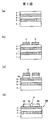
図1(a)~図1(d)は、本発明の一実施形態に係る種結晶基板8Aの各製造工程を示す模式図である。
図2は、種結晶基板8A上に窒化ガリウム単結晶7を育成した状態を示す模式図である。
図3(a)~(d)は、本発明の他の実施形態に係る種結晶基板8Bの各製造工程を示す模式図である。
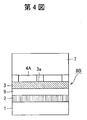
図4は、種結晶基板8B上に窒化ガリウム単結晶7を育成した状態を示す模式図である。
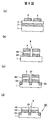
図5(a)~図5(d)は、本発明の更に他の実施形態に係る種結晶基板8Cの各製造工程を示す模式図である。
図6(a)~図6(d)は、本発明の更に他の実施形態に係る種結晶基板8Dの各製造工程を示す模式図である。
図7(a)~図7(d)は、本発明の更に他の実施形態に係る種結晶基板8Eの各製造工程を示す模式図である。
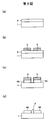
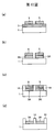
図8(a)~図8(d)は、比較例に係る種結晶基板の各製造工程を示す模式図である。
図9(a)~図9(d)は、他の比較例に係る種結晶基板の各製造工程を示す模式図である。
図10(a)~図10(d)は、更に他の比較例に係る種結晶基板の各製造工程を示す模式図である。 FIG. 1A to FIG. 1D are schematic views showing each manufacturing process of theseed crystal substrate 8A according to one embodiment of the present invention.
FIG. 2 is a schematic diagram showing a state in which the gallium nitridesingle crystal 7 is grown on the seed crystal substrate 8A.
FIGS. 3A to 3D are schematic views showing respective manufacturing steps of theseed crystal substrate 8B according to another embodiment of the present invention.
FIG. 4 is a schematic diagram showing a state in which the gallium nitridesingle crystal 7 is grown on the seed crystal substrate 8B.
5 (a) to 5 (d) are schematic views showing each manufacturing process of the seed crystal substrate 8C according to still another embodiment of the present invention.
6 (a) to 6 (d) are schematic views showing each manufacturing process of theseed crystal substrate 8D according to still another embodiment of the present invention.
FIG. 7A to FIG. 7D are schematic views showing each manufacturing process of theseed crystal substrate 8E according to still another embodiment of the present invention.
FIG. 8A to FIG. 8D are schematic views showing each manufacturing process of the seed crystal substrate according to the comparative example.
FIG. 9A to FIG. 9D are schematic views showing each manufacturing process of a seed crystal substrate according to another comparative example.
FIG. 10A to FIG. 10D are schematic views showing each manufacturing process of a seed crystal substrate according to still another comparative example.
図2は、種結晶基板8A上に窒化ガリウム単結晶7を育成した状態を示す模式図である。
図3(a)~(d)は、本発明の他の実施形態に係る種結晶基板8Bの各製造工程を示す模式図である。
図4は、種結晶基板8B上に窒化ガリウム単結晶7を育成した状態を示す模式図である。
図5(a)~図5(d)は、本発明の更に他の実施形態に係る種結晶基板8Cの各製造工程を示す模式図である。
図6(a)~図6(d)は、本発明の更に他の実施形態に係る種結晶基板8Dの各製造工程を示す模式図である。
図7(a)~図7(d)は、本発明の更に他の実施形態に係る種結晶基板8Eの各製造工程を示す模式図である。
図8(a)~図8(d)は、比較例に係る種結晶基板の各製造工程を示す模式図である。
図9(a)~図9(d)は、他の比較例に係る種結晶基板の各製造工程を示す模式図である。
図10(a)~図10(d)は、更に他の比較例に係る種結晶基板の各製造工程を示す模式図である。 FIG. 1A to FIG. 1D are schematic views showing each manufacturing process of the
FIG. 2 is a schematic diagram showing a state in which the gallium nitride
FIGS. 3A to 3D are schematic views showing respective manufacturing steps of the
FIG. 4 is a schematic diagram showing a state in which the gallium nitride
5 (a) to 5 (d) are schematic views showing each manufacturing process of the seed crystal substrate 8C according to still another embodiment of the present invention.
6 (a) to 6 (d) are schematic views showing each manufacturing process of the
FIG. 7A to FIG. 7D are schematic views showing each manufacturing process of the
FIG. 8A to FIG. 8D are schematic views showing each manufacturing process of the seed crystal substrate according to the comparative example.
FIG. 9A to FIG. 9D are schematic views showing each manufacturing process of a seed crystal substrate according to another comparative example.
FIG. 10A to FIG. 10D are schematic views showing each manufacturing process of a seed crystal substrate according to still another comparative example.
図1、図2の例では、低温バッファー層上に窒化アルミニウム単結晶または窒化アルミニウムガリウム単結晶からなる中間層を備えており、中間層が露出層を含む。
すなわち、図1(a)に示すように、支持基板1の表面に、III族窒化物からなる低温バッファー層2を形成する。次いで、低温バッファー層2上に、窒化アルミニウム単結晶または窒化アルミニウムガリウム単結晶からなる中間層3を形成する。ここで、低温バッファー層2と中間層3とはパターニングされていない。次いで、中間層3上に、窒化ガリウム単結晶からなる種結晶層4を形成する。
次いで、図1(b)に示すように、種結晶層4上にマスク5を形成し、図1(c)に示すように、種結晶層4をパターニングして、互いに分離された複数の種結晶層4Aを形成する。隣接する種結晶層4A間にには隙間が生ずる。次いで、図1(d)に示すようにマスク5を除去し、種結晶層4Aを露出させる。このとき、隣接する種結晶層4Aの隙間6から、下地となっている中間層3の露出層3aが露出する。
次いで、図2に示すように、種結晶層4A上に、フラックス法によって窒化ガリウム単結晶7をエピタキシャル成長させる。この際、層7は、種結晶4Aの隙間6上を横断して互いにつながるように成長し、一体の層7を形成する。この後、冷却時に、層7が低温バッファー層2に沿って支持基板1から容易に剥離するので、単結晶の自立基板を得ることができる。
また、他の実施形態においては、低温バッファー層上に窒化アルミニウム単結晶または窒化アルミニウムガリウム単結晶からなる中間層を設けると共に、中間層と低温バッファー層との間に窒化ガリウム単結晶層を設ける。図3、図4は、この実施形態に係るものである。
すなわち、図3(a)に示すように、支持基板1の表面に、III族窒化物からなる低温バッファー層2を形成する。次いで、低温バッファー層2上に、窒化ガリウム単結晶層9、窒化アルミニウム単結晶または窒化アルミニウムガリウム単結晶からなる中間層3を順次形成する。ここで、低温バッファー層2、窒化ガリウム単結晶層9,中間層3はパターニングされていない。次いで、中間層3上に、窒化ガリウム単結晶からなる種結晶層4を形成する。
次いで、図3(b)に示すように、種結晶層4上にマスク5を形成し、図3(c)に示すように、種結晶層4をパターニングして、互いに分離された複数の種結晶層4Aを形成する。隣接する種結晶層4A間にには隙間が生ずる。次いで、図3(d)に示すようにマスク5を除去し、種結晶層4Aを露出させる。このとき、隣接する種結晶層4Aの隙間6から、下地となっている中間層3の露出層3aが露出する。
次いで、図4に示すように、種結晶層4A上に、フラックス法によって窒化ガリウム単結晶7をエピタキシャル成長させる。この際、層7は、種結晶4Aの隙間6上を横断して互いにつながるように成長し、一体の層7を形成する。この後、冷却時に、層7が低温バッファー層2に沿って支持基板1から容易に剥離するので、単結晶の自立基板を得ることができる。
また、好適な実施形態においては、低温バッファー層が複数の分離部に分離されており、隣接する分離部の隙間が種結晶層間の隙間と連通しており、支持基板の表面に露出層が成層されている。図5はこの実施形態に係るものである。
図5(a)に示すように、支持基板1の表面に、III族窒化物からなる低温バッファー層2を形成する。次いで、低温バッファー層2上に、中間層を設けることなく、窒化ガリウム単結晶からなる種結晶層4を形成する。次いで、種結晶層4上にマスク5を形成し、図5(b)に示すように、種結晶層4、低温バッファー層2をパターニングして、互いに分離された複数の種結晶層4Aおよび低温バッファー層2Aを形成する。隣接する種結晶層4A間、隣接する低温バッファー層2A間には隙間6が生ずる。
次いで、図5(c)に示すように、隙間6内に、窒化アルミニウム単結晶または窒化アルミニウムガリウム単結晶からなる露出層13を成層する。次いで、マスク5を除去し、種結晶層4Aを露出させる。このとき、隣接する種結晶層4A、隣接する分離部2Aの隙間6から、露出層13の露出面が露出する。
次いで、例えば図2に示すように、種結晶層4A上に、フラックス法によって窒化ガリウム単結晶7をエピタキシャル成長させる。この際、層7は、種結晶4A層の隙間6上を横断して互いにつながるように成長し、一体の層7を形成する。この後、冷却時に、層7が低温バッファー層2Aに沿って支持基板1から容易に剥離するので、単結晶の自立基板を得ることができる。
また、他の実施形態においては、低温バッファー層が複数の分離部に分離されており、隣接する分離部の隙間が種結晶層間の隙間と連通しており、支持基板がサファイアからなり、支持基板に表面窒化処理によって露出層が形成されている。図6はこの実施形態に係るものである。
図6(a)に示すように、支持基板1の表面に、III族窒化物からなる低温バッファー層2を形成する。次いで、低温バッファー層2上に、中間層を設けることなく、窒化ガリウム単結晶からなる種結晶層4を形成する。次いで、種結晶層4上にマスク5を形成し、図6(b)に示すように、種結晶層4、低温バッファー層2をパターニングして、互いに分離された複数の種結晶層4Aおよび低温バッファー層2Aを形成する。隣接する種結晶層4A間、隣接する低温バッファー層2A間には隙間6が生ずる。
次いで、図6(c)に示すように、隙間6内において、支持基板1を表面窒化し、窒化アルミニウム単結晶からなる露出層23を成層する。次いで、マスク5を除去し、種結晶層4Aを露出させる。このとき、隣接する種結晶層4A、隣接する分離部2Aの隙間6から、露出層13の露出面が露出する。
次いで、例えば図2に示すように、種結晶層4A上に、フラックス法によって窒化ガリウム単結晶7をエピタキシャル成長させる。この際、層7は、種結晶4A層の隙間6上を横断して互いにつながるように成長し、一体の層7を形成する。この後、冷却時に、層7が低温バッファー層2Aに沿って支持基板1から容易に剥離するので、単結晶の自立基板を得ることができる。
また、他の実施形態においては、低温バッファー層と支持基板との間に設けられた窒化アルミニウム単結晶または窒化アルミニウムガリウム単結晶層を備えており、低温バッファー層は複数の分離部に分離され、隣接する分離部の隙間が種結晶層間の隙間と連通しており、隙間に前記窒化アルミニウム単結晶または窒化アルミニウムガリウム単結晶層が露出している。図7はこの実施形態に係るものである。
図7(a)に示すように、支持基板1の表面に、窒化アルミニウム単結晶層または窒化アルミニウムガリウム単結晶層3、低温バッファー層2、窒化ガリウム単結晶からなる種結晶層4を形成する。
次いで、図7(b)に示すように、種結晶層4上にマスク5を形成し、図7(c)に示すように、種結晶層4、低温バッファー層2をパターニングして、互いに分離された複数の種結晶層4Aおよび低温バッファー層2Aを形成する。隣接する種結晶層4A間、隣接する低温バッファー層2A間には隙間6が生じ、隙間6から、下地となっている窒化アルミニウム単結晶層または窒化アルミニウムガリウム単結晶層3の露出層3aが露出する。
次いで、例えば図2に示すように、種結晶層4A上に、フラックス法によって窒化ガリウム単結晶7をエピタキシャル成長させる。この際、層7は、種結晶4A層の隙間6上を横断して互いにつながるように成長し、一体の層7を形成する。この後、冷却時に、層7が低温バッファー層2Aに沿って支持基板1から容易に剥離するので、単結晶の自立基板を得ることができる。
本発明においては、支持基板1は、III族窒化物の成長が可能であるかぎり、特に限定されない。サファイア、シリコン単結晶、SiC単結晶、MgO単結晶、ZnO単結晶、スピネル(MgAl2O4)、LiAlO2、LiGaO2、LaAlO3,LaGaO3,NdGaO3等のペロブスカイト型複合酸化物を例示できる。また:組成式〔A1−y(Sr1−xBax)y〕〔(Al1−zGaz)1−u・Du〕O3(Aは、希土類元素である;Dは、ニオブおよびタンタルからなる群より選ばれた一種以上の元素である;y=0.3~0.98;x=0~1;z=0~1;u=0.15~0.49;x+z=0.1~2)の立方晶系のペロブスカイト構造複合酸化物も使用できる。また、SCAM(ScAlMgO4)も使用できる。
III族金属窒化物のウルツ鉱構造は、c面、a面、およびm面を有する。これらの各結晶面は結晶学的に定義されるものである。低温バッファー層、中間層、種結晶層、およびフラックス法によって育成される窒化ガリウム単結晶の育成方向は、c面の法線方向であってよく、またa面、m面などの無極性面やR面などの半極性面のそれぞれの法線方向であってもよい。
低温バッファー層を構成するIII族窒化物は、Ga、Al、Inから選ばれた一種以上の金属の窒化物であることが好ましく、GaN、AlN、AlGaNなどが特に好ましい。さらに、これらの窒化物には意図しない不純物元素を含んでいても良い。また導電性を制御するために、意図的に添加したSi,Ge,Be,Mg,Zn,Cdなどのドーパントを含んでいても良い。
低温バッファー層、種結晶層の形成方法は気相成長法が好ましいが、有機金属化学気相成長(MOCVD: Metal Organic Chemical Vapor Deposition)法、ハイドライド気相成長(HVPE)法、パルス励起堆積(PXD)法、MBE法、昇華法を例示できる。有機金属化学気相成長法が特に好ましい。
低温バッファー層の厚さは特に限定されないが、10nm以上が好ましく、また、500nm以下が好ましく、250nm以下が更に好ましい。種結晶層の厚さは特に限定されないが、種結晶層のメルトバックを抑制するという観点からは、0.5μm以上であることが好ましく、10μm以上であることがさらに好ましい。また、種結晶層を厚くすると、種結晶層の形成に時間がかかるので、この観点からは、種結晶層の厚さを50μm以下とすることが好ましい。
単結晶の基板からの剥離を促進するという観点からは、低温バッファー層の育成温度よりも、種結晶層の育成温度の方が高い方が好ましい。この温度差は、100℃以上であることが好ましく、200℃以上であることが更に好ましい。
低温バッファー層の育成温度は、400℃以上とすることが好ましく、450℃以上とすることが更に好ましく、また、750℃以下とすることが好ましく、700℃以下とすることが更に好ましい。単結晶層の育成温度は、950℃以上とすることが好ましく、1050℃以上とすることが更に好ましく、また、1200℃以下とすることが好ましく、1150℃以下とすることが更に好ましい。
種結晶層を有機金属気相成長法によって製造する場合、原料は、トリメチルガリウム(TMG)及びアンモニアとすることが好ましい。
低温バッファー層は前述したように相対的に低温で形成されるので、次の種結晶層を育成するときに低温バッファー層の成分が蒸発し、低温バッファー層に空隙を生成することがある。この場合には、種結晶層の結晶品質が劣化し、その結果、単結晶7の結晶品質も劣化するおそれがある。このため、好適な実施形態においては、低温バッファー層2を形成した後に、低温バッファー層2の構成成分の蒸発を防止するための蒸発防止層を形成する。これによって、種結晶層を育成する段階で低温バッファー層2内に空隙が形成されることを防止し、種結晶層の結晶品質の劣化を抑えることができる。こうした蒸発防止層の材質としては、GaN、AlN、AlGaNなどを例示できる。
蒸発防止層は、前述したような気相成長法で育成できる。蒸発防止層の育成温度は、400~900℃であることが好ましい。蒸発防止層の育成温度と中間層の育成温度との差は、0~100℃であることが更に好ましい。
本実施形態において特に好ましくは、低温バッファー層の材質がInGaN、InAlNまたはInAlGaNであり、蒸発しやすい成分がInである。そして、蒸発防止層の材質がGaN、AlNまたはAlGaNである。このような蒸発防止層は、InGaN、InAlNまたはInAlGaNの形成時にIn原料ガスの供給だけを停止することによって容易に育成できる。
また、低温バッファー層が超格子構造からなる場合には、超格子構造内の薄層に蒸発防止層としての機能をもたせることができるので、やはり中間層内での空隙の形成を防止できる。この場合には、蒸発防止層は特に必要としない。
露出層、特に露出層を含む中間層は、窒化アルミニウム単結晶または窒化アルミニウムガリウム単結晶からなる。ここで、窒化アルミニウムガリウム単結晶におけるアルミニウムの原子比率は、30%以上が好ましい。
露出層、中間層の形成方法は気相成長法が好ましいが、有機金属化学気相成長(MOCVD: Metal Organic Chemical Vapor Deposition)法、ハイドライド気相成長(HVPE)法、パルス励起堆積(PXD)法、MBE法、昇華法を例示できる。有機金属化学気相成長法が特に好ましい。
露出層、中間層の厚さは特に限定されないが、10nm以上が好ましく、また、500nm以下が好ましく、250nm以下が更に好ましい。また、露出層、中間層の育成温度は、950℃以上とすることが好ましく、1050℃以上とすることが更に好ましく、また、1200℃以下とすることが好ましい。
露出層、中間層を有機金属気相成長法によって製造する場合、原料は、トリメチルアルミニウム、トリメチルガリウム、アンモニアとすることが好ましい。
支持基板の窒化処理によって露出層23を形成する場合には、支持基板の材質はサファイアが好ましい。また窒化処理を行うには、窒素含有雰囲気下で支持基板をアニール処理する。このときのアニール温度は800~1200℃が好ましい。
各種結晶層の最小幅は、単結晶の品質向上という観点からは、600μm以下が好ましく、400μm以下が更に好ましい。また、単結晶育成時に単結晶7を安定して保持するという観点からは、10μm以上が好ましく、25μm以上が更に好ましい。ここで、種結晶層の最小幅とは、種結晶層の輪郭の任意の二点を結ぶ直線の中で、最短の直線の長さを言う。したがって、種結晶層が帯状ないしストライプ状の場合にはその短辺の長さであり、種結晶層が円形の場合には直径であり、種結晶層が正多角形の場合には一対の対向片の間隔である。
種結晶層の隙間6の間隔は、単結晶の品質向上という観点からは、250μm以上が好ましく、500μm以上が好ましい。この間隔は、隣り合う種結晶層から成長した各単結晶が互いに接続して一体化するのを促進するという観点からは、4000μm以下が好ましく3000μm以下が更に好ましい。
本発明においては、種結晶層上にフラックス法によって窒化ガリウム層7を育成する。この際、フラックスの種類は、窒化ガリウムを生成可能である限り、特に限定されない。好適な実施形態においては、アルカリ金属とアルカリ土類金属の少なくとも一方を含むフラックスを使用し、ナトリウム金属を含むフラックスが特に好ましい。
ガリウム原料物質としては、ガリウム単体金属、ガリウム合金、ガリウム化合物を適用できるが、ガリウム単体金属が取扱いの上からも好適である。
フラックス法におけるIII族窒化物単結晶の育成温度や育成時の保持時間は特に限定されず、目的とする単結晶の種類やフラックスの組成に応じて適宜変更する。一例では、ナトリウムまたはリチウム含有フラックスを用いて窒化ガリウム単結晶を育成する場合には、育成温度を800~1000℃とすることができる。
フラックス法では、窒素原子を含む分子を含むガス雰囲気下で単結晶を育成する。このガスは窒素ガスが好ましいが、アンモニアでもよい。雰囲気の全圧は特に限定されないが、フラックスの蒸発を防止する観点からは、1MPa以上が好ましく、3MPa以上が更に好ましい。ただし、圧力が高いと装置が大がかりとなるので、雰囲気の全圧は、200MPa以下が好ましく、50MPa以下が更に好ましい。雰囲気中の窒素以外のガスは限定されないが、不活性ガスが好ましく、アルゴン、ヘリウム、ネオンが特に好ましい。 In the example of FIGS. 1 and 2, an intermediate layer made of an aluminum nitride single crystal or an aluminum gallium nitride single crystal is provided on the low-temperature buffer layer, and the intermediate layer includes an exposed layer.
That is, as shown in FIG. 1A, a low-temperature buffer layer 2 made of a group III nitride is formed on the surface of the support substrate 1. Next, an intermediate layer 3 made of an aluminum nitride single crystal or an aluminum gallium nitride single crystal is formed on the low-temperature buffer layer 2. Here, the low temperature buffer layer 2 and the intermediate layer 3 are not patterned. Next, a seed crystal layer 4 made of a gallium nitride single crystal is formed on the intermediate layer 3.
Next, as shown in FIG. 1B, amask 5 is formed on the seed crystal layer 4, and the seed crystal layer 4 is patterned as shown in FIG. A crystal layer 4A is formed. A gap is generated between adjacent seed crystal layers 4A. Next, as shown in FIG. 1D, the mask 5 is removed to expose the seed crystal layer 4A. At this time, the exposed layer 3a of the intermediate layer 3 serving as the base is exposed from the gap 6 between the adjacent seed crystal layers 4A.
Next, as shown in FIG. 2, a gallium nitridesingle crystal 7 is epitaxially grown on the seed crystal layer 4A by a flux method. At this time, the layer 7 grows so as to cross over the gap 6 of the seed crystal 4A and to be connected to each other, thereby forming an integral layer 7. Thereafter, the layer 7 is easily peeled from the support substrate 1 along the low-temperature buffer layer 2 during cooling, so that a single-crystal free-standing substrate can be obtained.
In another embodiment, an intermediate layer made of an aluminum nitride single crystal or an aluminum gallium nitride single crystal is provided on the low temperature buffer layer, and a gallium nitride single crystal layer is provided between the intermediate layer and the low temperature buffer layer. 3 and 4 relate to this embodiment.
That is, as shown in FIG. 3A, a low-temperature buffer layer 2 made of a group III nitride is formed on the surface of the support substrate 1. Next, a gallium nitride single crystal layer 9 and an intermediate layer 3 made of an aluminum nitride single crystal or an aluminum gallium nitride single crystal are sequentially formed on the low temperature buffer layer 2. Here, the low temperature buffer layer 2, the gallium nitride single crystal layer 9, and the intermediate layer 3 are not patterned. Next, a seed crystal layer 4 made of a gallium nitride single crystal is formed on the intermediate layer 3.
Next, amask 5 is formed on the seed crystal layer 4 as shown in FIG. 3B, and the seed crystal layer 4 is patterned as shown in FIG. A crystal layer 4A is formed. A gap is generated between adjacent seed crystal layers 4A. Next, as shown in FIG. 3D, the mask 5 is removed, and the seed crystal layer 4A is exposed. At this time, the exposed layer 3a of the intermediate layer 3 serving as the base is exposed from the gap 6 between the adjacent seed crystal layers 4A.
Next, as shown in FIG. 4, a gallium nitridesingle crystal 7 is epitaxially grown on the seed crystal layer 4A by a flux method. At this time, the layer 7 grows so as to cross over the gap 6 of the seed crystal 4A and to be connected to each other, thereby forming an integral layer 7. Thereafter, the layer 7 is easily peeled from the support substrate 1 along the low-temperature buffer layer 2 during cooling, so that a single-crystal free-standing substrate can be obtained.
In a preferred embodiment, the low-temperature buffer layer is separated into a plurality of separation parts, the gaps between adjacent separation parts communicate with the gaps between the seed crystal layers, and the exposed layer is formed on the surface of the support substrate. Has been. FIG. 5 relates to this embodiment.
As shown in FIG. 5A, a low-temperature buffer layer 2 made of a group III nitride is formed on the surface of the support substrate 1. Next, a seed crystal layer 4 made of a gallium nitride single crystal is formed on the low-temperature buffer layer 2 without providing an intermediate layer. Next, a mask 5 is formed on the seed crystal layer 4, and as shown in FIG. 5B, the seed crystal layer 4 and the low-temperature buffer layer 2 are patterned to form a plurality of seed crystal layers 4A and low-temperature layers separated from each other. The buffer layer 2A is formed. A gap 6 is formed between the adjacent seed crystal layers 4A and between the adjacent low-temperature buffer layers 2A.
Next, as shown in FIG. 5C, an exposedlayer 13 made of an aluminum nitride single crystal or an aluminum gallium nitride single crystal is formed in the gap 6. Next, the mask 5 is removed, and the seed crystal layer 4A is exposed. At this time, the exposed surface of the exposed layer 13 is exposed from the adjacent seed crystal layer 4A and the gap 6 between the adjacent separating portions 2A.
Next, for example, as shown in FIG. 2, a gallium nitridesingle crystal 7 is epitaxially grown on the seed crystal layer 4A by a flux method. At this time, the layer 7 grows so as to cross the gap 6 of the seed crystal 4A layer and to be connected to each other, thereby forming an integral layer 7. Thereafter, during cooling, the layer 7 is easily peeled off from the support substrate 1 along the low-temperature buffer layer 2A, so that a single crystal free-standing substrate can be obtained.
In another embodiment, the low-temperature buffer layer is separated into a plurality of separation parts, the gap between adjacent separation parts communicates with the gap between the seed crystal layers, the support substrate is made of sapphire, and the support substrate An exposed layer is formed by surface nitriding. FIG. 6 relates to this embodiment.
As shown in FIG. 6A, a lowtemperature buffer layer 2 made of a group III nitride is formed on the surface of the support substrate 1. Next, a seed crystal layer 4 made of a gallium nitride single crystal is formed on the low-temperature buffer layer 2 without providing an intermediate layer. Next, a mask 5 is formed on the seed crystal layer 4, and as shown in FIG. 6B, the seed crystal layer 4 and the low-temperature buffer layer 2 are patterned to form a plurality of seed crystal layers 4A and low-temperature layers separated from each other. The buffer layer 2A is formed. A gap 6 is formed between the adjacent seed crystal layers 4A and between the adjacent low-temperature buffer layers 2A.
Next, as shown in FIG. 6C, thesupport substrate 1 is surface nitrided in the gap 6 to form an exposed layer 23 made of an aluminum nitride single crystal. Next, the mask 5 is removed, and the seed crystal layer 4A is exposed. At this time, the exposed surface of the exposed layer 13 is exposed from the adjacent seed crystal layer 4A and the gap 6 between the adjacent separating portions 2A.
Next, for example, as shown in FIG. 2, a gallium nitridesingle crystal 7 is epitaxially grown on the seed crystal layer 4A by a flux method. At this time, the layer 7 grows so as to cross the gap 6 of the seed crystal 4A layer and to be connected to each other, thereby forming an integral layer 7. Thereafter, during cooling, the layer 7 is easily peeled off from the support substrate 1 along the low-temperature buffer layer 2A, so that a single crystal free-standing substrate can be obtained.
Further, in another embodiment, it comprises an aluminum nitride single crystal or an aluminum gallium nitride single crystal layer provided between the low temperature buffer layer and the support substrate, the low temperature buffer layer is separated into a plurality of separation parts, A gap between adjacent separation portions communicates with a gap between seed crystal layers, and the aluminum nitride single crystal or aluminum gallium nitride single crystal layer is exposed in the gap. FIG. 7 relates to this embodiment.
As shown in FIG. 7A, an aluminum nitride single crystal layer or an aluminum gallium nitridesingle crystal layer 3, a low-temperature buffer layer 2, and a seed crystal layer 4 made of gallium nitride single crystal are formed on the surface of the support substrate 1.
Next, as shown in FIG. 7 (b), amask 5 is formed on the seed crystal layer 4, and as shown in FIG. 7 (c), the seed crystal layer 4 and the low-temperature buffer layer 2 are patterned and separated from each other. The plurality of seed crystal layers 4A and the low-temperature buffer layer 2A thus formed are formed. A gap 6 is formed between the adjacent seed crystal layers 4A and between the adjacent low-temperature buffer layers 2A, and the exposed layer 3a of the underlying aluminum nitride single crystal layer or aluminum gallium nitride single crystal layer 3 is exposed from the gap 6. To do.
Next, for example, as shown in FIG. 2, a gallium nitridesingle crystal 7 is epitaxially grown on the seed crystal layer 4A by a flux method. At this time, the layer 7 grows so as to cross the gap 6 of the seed crystal 4A layer and to be connected to each other, thereby forming an integral layer 7. Thereafter, during cooling, the layer 7 is easily peeled off from the support substrate 1 along the low-temperature buffer layer 2A, so that a single crystal free-standing substrate can be obtained.
In the present invention, thesupport substrate 1 is not particularly limited as long as the group III nitride can be grown. Perovskite type complex oxides such as sapphire, silicon single crystal, SiC single crystal, MgO single crystal, ZnO single crystal, spinel (MgAl 2 O 4 ), LiAlO 2 , LiGaO 2 , LaAlO 3 , LaGaO 3 , NdGaO 3 can be exemplified. . Also: the composition formula [A 1-y (Sr 1- x Ba x) y ] [(Al 1-z Ga z) 1-u · D u ] O 3 (A is a rare earth element; D is niobium And one or more elements selected from the group consisting of tantalum; y = 0.3 to 0.98; x = 0 to 1; z = 0 to 1; u = 0.15 to 0.49; x + z = A cubic perovskite structure composite oxide of 0.1 to 2) can also be used. SCAM (ScAlMgO 4 ) can also be used.
The wurtzite structure of Group III metal nitride has a c-plane, a-plane, and m-plane. Each of these crystal planes is defined crystallographically. The growth direction of the low-temperature buffer layer, the intermediate layer, the seed crystal layer, and the gallium nitride single crystal grown by the flux method may be the normal direction of the c-plane, Each normal direction of a semipolar plane such as an R plane may be used.
The group III nitride constituting the low-temperature buffer layer is preferably a nitride of one or more metals selected from Ga, Al, and In, and GaN, AlN, AlGaN, and the like are particularly preferable. Further, these nitrides may contain an unintended impurity element. Moreover, in order to control electroconductivity, you may include dopants, such as Si, Ge, Be, Mg, Zn, Cd added intentionally.
The low-temperature buffer layer and the seed crystal layer are preferably formed by vapor deposition, but metal organic chemical vapor deposition (MOCVD), hydride vapor deposition (HVPE), pulsed excitation deposition (PXD) ) Method, MBE method, and sublimation method. Metalorganic chemical vapor deposition is particularly preferred.
The thickness of the low-temperature buffer layer is not particularly limited, but is preferably 10 nm or more, preferably 500 nm or less, and more preferably 250 nm or less. The thickness of the seed crystal layer is not particularly limited, but is preferably 0.5 μm or more and more preferably 10 μm or more from the viewpoint of suppressing the meltback of the seed crystal layer. In addition, when the seed crystal layer is thickened, it takes time to form the seed crystal layer. From this viewpoint, the thickness of the seed crystal layer is preferably 50 μm or less.
From the viewpoint of promoting the peeling of the single crystal from the substrate, the growth temperature of the seed crystal layer is preferably higher than the growth temperature of the low-temperature buffer layer. This temperature difference is preferably 100 ° C. or higher, and more preferably 200 ° C. or higher.
The growth temperature of the low temperature buffer layer is preferably 400 ° C. or higher, more preferably 450 ° C. or higher, more preferably 750 ° C. or lower, and still more preferably 700 ° C. or lower. The growth temperature of the single crystal layer is preferably 950 ° C. or higher, more preferably 1050 ° C. or higher, more preferably 1200 ° C. or lower, and further preferably 1150 ° C. or lower.
When the seed crystal layer is manufactured by a metal organic vapor phase epitaxy method, the raw materials are preferably trimethylgallium (TMG) and ammonia.
Since the low-temperature buffer layer is formed at a relatively low temperature as described above, the components of the low-temperature buffer layer may evaporate when the next seed crystal layer is grown, and voids may be generated in the low-temperature buffer layer. In this case, the crystal quality of the seed crystal layer is degraded, and as a result, the crystal quality of thesingle crystal 7 may be degraded. For this reason, in a preferred embodiment, after the low temperature buffer layer 2 is formed, an evaporation preventing layer for preventing evaporation of the constituent components of the low temperature buffer layer 2 is formed. Thereby, it is possible to prevent voids from being formed in the low-temperature buffer layer 2 at the stage of growing the seed crystal layer, and to suppress the deterioration of the crystal quality of the seed crystal layer. Examples of the material for such an evaporation preventing layer include GaN, AlN, AlGaN, and the like.
The evaporation prevention layer can be grown by the vapor phase growth method as described above. The growth temperature of the evaporation preventing layer is preferably 400 to 900 ° C. The difference between the growth temperature of the evaporation preventing layer and the growth temperature of the intermediate layer is more preferably 0 to 100 ° C.
In the present embodiment, the material of the low-temperature buffer layer is particularly preferably InGaN, InAlN, or InAlGaN, and the component that easily evaporates is In. The material of the evaporation preventing layer is GaN, AlN or AlGaN. Such an evaporation prevention layer can be easily grown by stopping only the supply of the In source gas when forming InGaN, InAlN, or InAlGaN.
In addition, when the low-temperature buffer layer has a superlattice structure, the thin layer in the superlattice structure can have a function as an evaporation preventing layer, so that formation of voids in the intermediate layer can also be prevented. In this case, the evaporation preventing layer is not particularly required.
The exposed layer, particularly the intermediate layer including the exposed layer is made of an aluminum nitride single crystal or an aluminum gallium nitride single crystal. Here, the atomic ratio of aluminum in the aluminum gallium nitride single crystal is preferably 30% or more.
The formation method of the exposed layer and the intermediate layer is preferably a vapor deposition method, but a metal organic chemical vapor deposition (MOCVD) method, a hydride vapor deposition (HVPE) method, a pulsed excitation deposition (PXD) method. MBE method and sublimation method. Metalorganic chemical vapor deposition is particularly preferred.
Although the thickness of an exposed layer and an intermediate | middle layer is not specifically limited, 10 nm or more is preferable, 500 nm or less is preferable and 250 nm or less is still more preferable. The growth temperature of the exposed layer and the intermediate layer is preferably 950 ° C. or higher, more preferably 1050 ° C. or higher, and preferably 1200 ° C. or lower.
When the exposed layer and the intermediate layer are produced by metal organic vapor phase epitaxy, the raw materials are preferably trimethylaluminum, trimethylgallium and ammonia.
When the exposedlayer 23 is formed by nitriding the support substrate, the support substrate is preferably made of sapphire. In order to perform nitriding, the support substrate is annealed in a nitrogen-containing atmosphere. The annealing temperature at this time is preferably 800 to 1200 ° C.
The minimum width of the various crystal layers is preferably 600 μm or less, and more preferably 400 μm or less, from the viewpoint of improving the quality of the single crystal. Further, from the viewpoint of stably holding thesingle crystal 7 during single crystal growth, it is preferably 10 μm or more, and more preferably 25 μm or more. Here, the minimum width of the seed crystal layer refers to the length of the shortest straight line among the straight lines connecting any two points on the contour of the seed crystal layer. Therefore, when the seed crystal layer is a strip or stripe, it is the length of the short side, when the seed crystal layer is circular, it is the diameter, and when the seed crystal layer is a regular polygon, a pair of opposing It is the interval of the pieces.
The distance between thegaps 6 in the seed crystal layer is preferably 250 μm or more, more preferably 500 μm or more, from the viewpoint of improving the quality of the single crystal. This distance is preferably 4000 μm or less, and more preferably 3000 μm or less, from the viewpoint of facilitating connection and integration of single crystals grown from adjacent seed crystal layers.
In the present invention, thegallium nitride layer 7 is grown on the seed crystal layer by a flux method. At this time, the type of flux is not particularly limited as long as gallium nitride can be generated. In a preferred embodiment, a flux containing at least one of an alkali metal and an alkaline earth metal is used, and a flux containing sodium metal is particularly preferred.
As the gallium source material, a gallium simple metal, a gallium alloy, and a gallium compound can be applied, but a gallium simple metal is also preferable in terms of handling.
The growth temperature of the group III nitride single crystal and the holding time at the time of growth in the flux method are not particularly limited, and are appropriately changed according to the type of target single crystal and the composition of the flux. In one example, when a gallium nitride single crystal is grown using a sodium or lithium-containing flux, the growth temperature can be set to 800 to 1000 ° C.
In the flux method, a single crystal is grown in a gas atmosphere containing molecules containing nitrogen atoms. This gas is preferably nitrogen gas, but may be ammonia. The total pressure of the atmosphere is not particularly limited, but is preferably 1 MPa or more, more preferably 3 MPa or more, from the viewpoint of preventing evaporation of the flux. However, since the apparatus becomes large when the pressure is high, the total pressure in the atmosphere is preferably 200 MPa or less, and more preferably 50 MPa or less. A gas other than nitrogen in the atmosphere is not limited, but an inert gas is preferable, and argon, helium, and neon are particularly preferable.
すなわち、図1(a)に示すように、支持基板1の表面に、III族窒化物からなる低温バッファー層2を形成する。次いで、低温バッファー層2上に、窒化アルミニウム単結晶または窒化アルミニウムガリウム単結晶からなる中間層3を形成する。ここで、低温バッファー層2と中間層3とはパターニングされていない。次いで、中間層3上に、窒化ガリウム単結晶からなる種結晶層4を形成する。
次いで、図1(b)に示すように、種結晶層4上にマスク5を形成し、図1(c)に示すように、種結晶層4をパターニングして、互いに分離された複数の種結晶層4Aを形成する。隣接する種結晶層4A間にには隙間が生ずる。次いで、図1(d)に示すようにマスク5を除去し、種結晶層4Aを露出させる。このとき、隣接する種結晶層4Aの隙間6から、下地となっている中間層3の露出層3aが露出する。
次いで、図2に示すように、種結晶層4A上に、フラックス法によって窒化ガリウム単結晶7をエピタキシャル成長させる。この際、層7は、種結晶4Aの隙間6上を横断して互いにつながるように成長し、一体の層7を形成する。この後、冷却時に、層7が低温バッファー層2に沿って支持基板1から容易に剥離するので、単結晶の自立基板を得ることができる。
また、他の実施形態においては、低温バッファー層上に窒化アルミニウム単結晶または窒化アルミニウムガリウム単結晶からなる中間層を設けると共に、中間層と低温バッファー層との間に窒化ガリウム単結晶層を設ける。図3、図4は、この実施形態に係るものである。
すなわち、図3(a)に示すように、支持基板1の表面に、III族窒化物からなる低温バッファー層2を形成する。次いで、低温バッファー層2上に、窒化ガリウム単結晶層9、窒化アルミニウム単結晶または窒化アルミニウムガリウム単結晶からなる中間層3を順次形成する。ここで、低温バッファー層2、窒化ガリウム単結晶層9,中間層3はパターニングされていない。次いで、中間層3上に、窒化ガリウム単結晶からなる種結晶層4を形成する。
次いで、図3(b)に示すように、種結晶層4上にマスク5を形成し、図3(c)に示すように、種結晶層4をパターニングして、互いに分離された複数の種結晶層4Aを形成する。隣接する種結晶層4A間にには隙間が生ずる。次いで、図3(d)に示すようにマスク5を除去し、種結晶層4Aを露出させる。このとき、隣接する種結晶層4Aの隙間6から、下地となっている中間層3の露出層3aが露出する。
次いで、図4に示すように、種結晶層4A上に、フラックス法によって窒化ガリウム単結晶7をエピタキシャル成長させる。この際、層7は、種結晶4Aの隙間6上を横断して互いにつながるように成長し、一体の層7を形成する。この後、冷却時に、層7が低温バッファー層2に沿って支持基板1から容易に剥離するので、単結晶の自立基板を得ることができる。
また、好適な実施形態においては、低温バッファー層が複数の分離部に分離されており、隣接する分離部の隙間が種結晶層間の隙間と連通しており、支持基板の表面に露出層が成層されている。図5はこの実施形態に係るものである。
図5(a)に示すように、支持基板1の表面に、III族窒化物からなる低温バッファー層2を形成する。次いで、低温バッファー層2上に、中間層を設けることなく、窒化ガリウム単結晶からなる種結晶層4を形成する。次いで、種結晶層4上にマスク5を形成し、図5(b)に示すように、種結晶層4、低温バッファー層2をパターニングして、互いに分離された複数の種結晶層4Aおよび低温バッファー層2Aを形成する。隣接する種結晶層4A間、隣接する低温バッファー層2A間には隙間6が生ずる。
次いで、図5(c)に示すように、隙間6内に、窒化アルミニウム単結晶または窒化アルミニウムガリウム単結晶からなる露出層13を成層する。次いで、マスク5を除去し、種結晶層4Aを露出させる。このとき、隣接する種結晶層4A、隣接する分離部2Aの隙間6から、露出層13の露出面が露出する。
次いで、例えば図2に示すように、種結晶層4A上に、フラックス法によって窒化ガリウム単結晶7をエピタキシャル成長させる。この際、層7は、種結晶4A層の隙間6上を横断して互いにつながるように成長し、一体の層7を形成する。この後、冷却時に、層7が低温バッファー層2Aに沿って支持基板1から容易に剥離するので、単結晶の自立基板を得ることができる。
また、他の実施形態においては、低温バッファー層が複数の分離部に分離されており、隣接する分離部の隙間が種結晶層間の隙間と連通しており、支持基板がサファイアからなり、支持基板に表面窒化処理によって露出層が形成されている。図6はこの実施形態に係るものである。
図6(a)に示すように、支持基板1の表面に、III族窒化物からなる低温バッファー層2を形成する。次いで、低温バッファー層2上に、中間層を設けることなく、窒化ガリウム単結晶からなる種結晶層4を形成する。次いで、種結晶層4上にマスク5を形成し、図6(b)に示すように、種結晶層4、低温バッファー層2をパターニングして、互いに分離された複数の種結晶層4Aおよび低温バッファー層2Aを形成する。隣接する種結晶層4A間、隣接する低温バッファー層2A間には隙間6が生ずる。
次いで、図6(c)に示すように、隙間6内において、支持基板1を表面窒化し、窒化アルミニウム単結晶からなる露出層23を成層する。次いで、マスク5を除去し、種結晶層4Aを露出させる。このとき、隣接する種結晶層4A、隣接する分離部2Aの隙間6から、露出層13の露出面が露出する。
次いで、例えば図2に示すように、種結晶層4A上に、フラックス法によって窒化ガリウム単結晶7をエピタキシャル成長させる。この際、層7は、種結晶4A層の隙間6上を横断して互いにつながるように成長し、一体の層7を形成する。この後、冷却時に、層7が低温バッファー層2Aに沿って支持基板1から容易に剥離するので、単結晶の自立基板を得ることができる。
また、他の実施形態においては、低温バッファー層と支持基板との間に設けられた窒化アルミニウム単結晶または窒化アルミニウムガリウム単結晶層を備えており、低温バッファー層は複数の分離部に分離され、隣接する分離部の隙間が種結晶層間の隙間と連通しており、隙間に前記窒化アルミニウム単結晶または窒化アルミニウムガリウム単結晶層が露出している。図7はこの実施形態に係るものである。
図7(a)に示すように、支持基板1の表面に、窒化アルミニウム単結晶層または窒化アルミニウムガリウム単結晶層3、低温バッファー層2、窒化ガリウム単結晶からなる種結晶層4を形成する。
次いで、図7(b)に示すように、種結晶層4上にマスク5を形成し、図7(c)に示すように、種結晶層4、低温バッファー層2をパターニングして、互いに分離された複数の種結晶層4Aおよび低温バッファー層2Aを形成する。隣接する種結晶層4A間、隣接する低温バッファー層2A間には隙間6が生じ、隙間6から、下地となっている窒化アルミニウム単結晶層または窒化アルミニウムガリウム単結晶層3の露出層3aが露出する。
次いで、例えば図2に示すように、種結晶層4A上に、フラックス法によって窒化ガリウム単結晶7をエピタキシャル成長させる。この際、層7は、種結晶4A層の隙間6上を横断して互いにつながるように成長し、一体の層7を形成する。この後、冷却時に、層7が低温バッファー層2Aに沿って支持基板1から容易に剥離するので、単結晶の自立基板を得ることができる。
本発明においては、支持基板1は、III族窒化物の成長が可能であるかぎり、特に限定されない。サファイア、シリコン単結晶、SiC単結晶、MgO単結晶、ZnO単結晶、スピネル(MgAl2O4)、LiAlO2、LiGaO2、LaAlO3,LaGaO3,NdGaO3等のペロブスカイト型複合酸化物を例示できる。また:組成式〔A1−y(Sr1−xBax)y〕〔(Al1−zGaz)1−u・Du〕O3(Aは、希土類元素である;Dは、ニオブおよびタンタルからなる群より選ばれた一種以上の元素である;y=0.3~0.98;x=0~1;z=0~1;u=0.15~0.49;x+z=0.1~2)の立方晶系のペロブスカイト構造複合酸化物も使用できる。また、SCAM(ScAlMgO4)も使用できる。
III族金属窒化物のウルツ鉱構造は、c面、a面、およびm面を有する。これらの各結晶面は結晶学的に定義されるものである。低温バッファー層、中間層、種結晶層、およびフラックス法によって育成される窒化ガリウム単結晶の育成方向は、c面の法線方向であってよく、またa面、m面などの無極性面やR面などの半極性面のそれぞれの法線方向であってもよい。
低温バッファー層を構成するIII族窒化物は、Ga、Al、Inから選ばれた一種以上の金属の窒化物であることが好ましく、GaN、AlN、AlGaNなどが特に好ましい。さらに、これらの窒化物には意図しない不純物元素を含んでいても良い。また導電性を制御するために、意図的に添加したSi,Ge,Be,Mg,Zn,Cdなどのドーパントを含んでいても良い。
低温バッファー層、種結晶層の形成方法は気相成長法が好ましいが、有機金属化学気相成長(MOCVD: Metal Organic Chemical Vapor Deposition)法、ハイドライド気相成長(HVPE)法、パルス励起堆積(PXD)法、MBE法、昇華法を例示できる。有機金属化学気相成長法が特に好ましい。
低温バッファー層の厚さは特に限定されないが、10nm以上が好ましく、また、500nm以下が好ましく、250nm以下が更に好ましい。種結晶層の厚さは特に限定されないが、種結晶層のメルトバックを抑制するという観点からは、0.5μm以上であることが好ましく、10μm以上であることがさらに好ましい。また、種結晶層を厚くすると、種結晶層の形成に時間がかかるので、この観点からは、種結晶層の厚さを50μm以下とすることが好ましい。
単結晶の基板からの剥離を促進するという観点からは、低温バッファー層の育成温度よりも、種結晶層の育成温度の方が高い方が好ましい。この温度差は、100℃以上であることが好ましく、200℃以上であることが更に好ましい。
低温バッファー層の育成温度は、400℃以上とすることが好ましく、450℃以上とすることが更に好ましく、また、750℃以下とすることが好ましく、700℃以下とすることが更に好ましい。単結晶層の育成温度は、950℃以上とすることが好ましく、1050℃以上とすることが更に好ましく、また、1200℃以下とすることが好ましく、1150℃以下とすることが更に好ましい。
種結晶層を有機金属気相成長法によって製造する場合、原料は、トリメチルガリウム(TMG)及びアンモニアとすることが好ましい。
低温バッファー層は前述したように相対的に低温で形成されるので、次の種結晶層を育成するときに低温バッファー層の成分が蒸発し、低温バッファー層に空隙を生成することがある。この場合には、種結晶層の結晶品質が劣化し、その結果、単結晶7の結晶品質も劣化するおそれがある。このため、好適な実施形態においては、低温バッファー層2を形成した後に、低温バッファー層2の構成成分の蒸発を防止するための蒸発防止層を形成する。これによって、種結晶層を育成する段階で低温バッファー層2内に空隙が形成されることを防止し、種結晶層の結晶品質の劣化を抑えることができる。こうした蒸発防止層の材質としては、GaN、AlN、AlGaNなどを例示できる。
蒸発防止層は、前述したような気相成長法で育成できる。蒸発防止層の育成温度は、400~900℃であることが好ましい。蒸発防止層の育成温度と中間層の育成温度との差は、0~100℃であることが更に好ましい。
本実施形態において特に好ましくは、低温バッファー層の材質がInGaN、InAlNまたはInAlGaNであり、蒸発しやすい成分がInである。そして、蒸発防止層の材質がGaN、AlNまたはAlGaNである。このような蒸発防止層は、InGaN、InAlNまたはInAlGaNの形成時にIn原料ガスの供給だけを停止することによって容易に育成できる。
また、低温バッファー層が超格子構造からなる場合には、超格子構造内の薄層に蒸発防止層としての機能をもたせることができるので、やはり中間層内での空隙の形成を防止できる。この場合には、蒸発防止層は特に必要としない。
露出層、特に露出層を含む中間層は、窒化アルミニウム単結晶または窒化アルミニウムガリウム単結晶からなる。ここで、窒化アルミニウムガリウム単結晶におけるアルミニウムの原子比率は、30%以上が好ましい。
露出層、中間層の形成方法は気相成長法が好ましいが、有機金属化学気相成長(MOCVD: Metal Organic Chemical Vapor Deposition)法、ハイドライド気相成長(HVPE)法、パルス励起堆積(PXD)法、MBE法、昇華法を例示できる。有機金属化学気相成長法が特に好ましい。
露出層、中間層の厚さは特に限定されないが、10nm以上が好ましく、また、500nm以下が好ましく、250nm以下が更に好ましい。また、露出層、中間層の育成温度は、950℃以上とすることが好ましく、1050℃以上とすることが更に好ましく、また、1200℃以下とすることが好ましい。
露出層、中間層を有機金属気相成長法によって製造する場合、原料は、トリメチルアルミニウム、トリメチルガリウム、アンモニアとすることが好ましい。
支持基板の窒化処理によって露出層23を形成する場合には、支持基板の材質はサファイアが好ましい。また窒化処理を行うには、窒素含有雰囲気下で支持基板をアニール処理する。このときのアニール温度は800~1200℃が好ましい。
各種結晶層の最小幅は、単結晶の品質向上という観点からは、600μm以下が好ましく、400μm以下が更に好ましい。また、単結晶育成時に単結晶7を安定して保持するという観点からは、10μm以上が好ましく、25μm以上が更に好ましい。ここで、種結晶層の最小幅とは、種結晶層の輪郭の任意の二点を結ぶ直線の中で、最短の直線の長さを言う。したがって、種結晶層が帯状ないしストライプ状の場合にはその短辺の長さであり、種結晶層が円形の場合には直径であり、種結晶層が正多角形の場合には一対の対向片の間隔である。
種結晶層の隙間6の間隔は、単結晶の品質向上という観点からは、250μm以上が好ましく、500μm以上が好ましい。この間隔は、隣り合う種結晶層から成長した各単結晶が互いに接続して一体化するのを促進するという観点からは、4000μm以下が好ましく3000μm以下が更に好ましい。
本発明においては、種結晶層上にフラックス法によって窒化ガリウム層7を育成する。この際、フラックスの種類は、窒化ガリウムを生成可能である限り、特に限定されない。好適な実施形態においては、アルカリ金属とアルカリ土類金属の少なくとも一方を含むフラックスを使用し、ナトリウム金属を含むフラックスが特に好ましい。
ガリウム原料物質としては、ガリウム単体金属、ガリウム合金、ガリウム化合物を適用できるが、ガリウム単体金属が取扱いの上からも好適である。
フラックス法におけるIII族窒化物単結晶の育成温度や育成時の保持時間は特に限定されず、目的とする単結晶の種類やフラックスの組成に応じて適宜変更する。一例では、ナトリウムまたはリチウム含有フラックスを用いて窒化ガリウム単結晶を育成する場合には、育成温度を800~1000℃とすることができる。
フラックス法では、窒素原子を含む分子を含むガス雰囲気下で単結晶を育成する。このガスは窒素ガスが好ましいが、アンモニアでもよい。雰囲気の全圧は特に限定されないが、フラックスの蒸発を防止する観点からは、1MPa以上が好ましく、3MPa以上が更に好ましい。ただし、圧力が高いと装置が大がかりとなるので、雰囲気の全圧は、200MPa以下が好ましく、50MPa以下が更に好ましい。雰囲気中の窒素以外のガスは限定されないが、不活性ガスが好ましく、アルゴン、ヘリウム、ネオンが特に好ましい。 In the example of FIGS. 1 and 2, an intermediate layer made of an aluminum nitride single crystal or an aluminum gallium nitride single crystal is provided on the low-temperature buffer layer, and the intermediate layer includes an exposed layer.
That is, as shown in FIG. 1A, a low-
Next, as shown in FIG. 1B, a
Next, as shown in FIG. 2, a gallium nitride
In another embodiment, an intermediate layer made of an aluminum nitride single crystal or an aluminum gallium nitride single crystal is provided on the low temperature buffer layer, and a gallium nitride single crystal layer is provided between the intermediate layer and the low temperature buffer layer. 3 and 4 relate to this embodiment.
That is, as shown in FIG. 3A, a low-
Next, a
Next, as shown in FIG. 4, a gallium nitride
In a preferred embodiment, the low-temperature buffer layer is separated into a plurality of separation parts, the gaps between adjacent separation parts communicate with the gaps between the seed crystal layers, and the exposed layer is formed on the surface of the support substrate. Has been. FIG. 5 relates to this embodiment.
As shown in FIG. 5A, a low-
Next, as shown in FIG. 5C, an exposed
Next, for example, as shown in FIG. 2, a gallium nitride
In another embodiment, the low-temperature buffer layer is separated into a plurality of separation parts, the gap between adjacent separation parts communicates with the gap between the seed crystal layers, the support substrate is made of sapphire, and the support substrate An exposed layer is formed by surface nitriding. FIG. 6 relates to this embodiment.
As shown in FIG. 6A, a low
Next, as shown in FIG. 6C, the
Next, for example, as shown in FIG. 2, a gallium nitride
Further, in another embodiment, it comprises an aluminum nitride single crystal or an aluminum gallium nitride single crystal layer provided between the low temperature buffer layer and the support substrate, the low temperature buffer layer is separated into a plurality of separation parts, A gap between adjacent separation portions communicates with a gap between seed crystal layers, and the aluminum nitride single crystal or aluminum gallium nitride single crystal layer is exposed in the gap. FIG. 7 relates to this embodiment.
As shown in FIG. 7A, an aluminum nitride single crystal layer or an aluminum gallium nitride
Next, as shown in FIG. 7 (b), a
Next, for example, as shown in FIG. 2, a gallium nitride
In the present invention, the
The wurtzite structure of Group III metal nitride has a c-plane, a-plane, and m-plane. Each of these crystal planes is defined crystallographically. The growth direction of the low-temperature buffer layer, the intermediate layer, the seed crystal layer, and the gallium nitride single crystal grown by the flux method may be the normal direction of the c-plane, Each normal direction of a semipolar plane such as an R plane may be used.
The group III nitride constituting the low-temperature buffer layer is preferably a nitride of one or more metals selected from Ga, Al, and In, and GaN, AlN, AlGaN, and the like are particularly preferable. Further, these nitrides may contain an unintended impurity element. Moreover, in order to control electroconductivity, you may include dopants, such as Si, Ge, Be, Mg, Zn, Cd added intentionally.
The low-temperature buffer layer and the seed crystal layer are preferably formed by vapor deposition, but metal organic chemical vapor deposition (MOCVD), hydride vapor deposition (HVPE), pulsed excitation deposition (PXD) ) Method, MBE method, and sublimation method. Metalorganic chemical vapor deposition is particularly preferred.
The thickness of the low-temperature buffer layer is not particularly limited, but is preferably 10 nm or more, preferably 500 nm or less, and more preferably 250 nm or less. The thickness of the seed crystal layer is not particularly limited, but is preferably 0.5 μm or more and more preferably 10 μm or more from the viewpoint of suppressing the meltback of the seed crystal layer. In addition, when the seed crystal layer is thickened, it takes time to form the seed crystal layer. From this viewpoint, the thickness of the seed crystal layer is preferably 50 μm or less.
From the viewpoint of promoting the peeling of the single crystal from the substrate, the growth temperature of the seed crystal layer is preferably higher than the growth temperature of the low-temperature buffer layer. This temperature difference is preferably 100 ° C. or higher, and more preferably 200 ° C. or higher.
The growth temperature of the low temperature buffer layer is preferably 400 ° C. or higher, more preferably 450 ° C. or higher, more preferably 750 ° C. or lower, and still more preferably 700 ° C. or lower. The growth temperature of the single crystal layer is preferably 950 ° C. or higher, more preferably 1050 ° C. or higher, more preferably 1200 ° C. or lower, and further preferably 1150 ° C. or lower.
When the seed crystal layer is manufactured by a metal organic vapor phase epitaxy method, the raw materials are preferably trimethylgallium (TMG) and ammonia.
Since the low-temperature buffer layer is formed at a relatively low temperature as described above, the components of the low-temperature buffer layer may evaporate when the next seed crystal layer is grown, and voids may be generated in the low-temperature buffer layer. In this case, the crystal quality of the seed crystal layer is degraded, and as a result, the crystal quality of the
The evaporation prevention layer can be grown by the vapor phase growth method as described above. The growth temperature of the evaporation preventing layer is preferably 400 to 900 ° C. The difference between the growth temperature of the evaporation preventing layer and the growth temperature of the intermediate layer is more preferably 0 to 100 ° C.
In the present embodiment, the material of the low-temperature buffer layer is particularly preferably InGaN, InAlN, or InAlGaN, and the component that easily evaporates is In. The material of the evaporation preventing layer is GaN, AlN or AlGaN. Such an evaporation prevention layer can be easily grown by stopping only the supply of the In source gas when forming InGaN, InAlN, or InAlGaN.
In addition, when the low-temperature buffer layer has a superlattice structure, the thin layer in the superlattice structure can have a function as an evaporation preventing layer, so that formation of voids in the intermediate layer can also be prevented. In this case, the evaporation preventing layer is not particularly required.
The exposed layer, particularly the intermediate layer including the exposed layer is made of an aluminum nitride single crystal or an aluminum gallium nitride single crystal. Here, the atomic ratio of aluminum in the aluminum gallium nitride single crystal is preferably 30% or more.
The formation method of the exposed layer and the intermediate layer is preferably a vapor deposition method, but a metal organic chemical vapor deposition (MOCVD) method, a hydride vapor deposition (HVPE) method, a pulsed excitation deposition (PXD) method. MBE method and sublimation method. Metalorganic chemical vapor deposition is particularly preferred.
Although the thickness of an exposed layer and an intermediate | middle layer is not specifically limited, 10 nm or more is preferable, 500 nm or less is preferable and 250 nm or less is still more preferable. The growth temperature of the exposed layer and the intermediate layer is preferably 950 ° C. or higher, more preferably 1050 ° C. or higher, and preferably 1200 ° C. or lower.
When the exposed layer and the intermediate layer are produced by metal organic vapor phase epitaxy, the raw materials are preferably trimethylaluminum, trimethylgallium and ammonia.
When the exposed
The minimum width of the various crystal layers is preferably 600 μm or less, and more preferably 400 μm or less, from the viewpoint of improving the quality of the single crystal. Further, from the viewpoint of stably holding the
The distance between the
In the present invention, the
As the gallium source material, a gallium simple metal, a gallium alloy, and a gallium compound can be applied, but a gallium simple metal is also preferable in terms of handling.
The growth temperature of the group III nitride single crystal and the holding time at the time of growth in the flux method are not particularly limited, and are appropriately changed according to the type of target single crystal and the composition of the flux. In one example, when a gallium nitride single crystal is grown using a sodium or lithium-containing flux, the growth temperature can be set to 800 to 1000 ° C.
In the flux method, a single crystal is grown in a gas atmosphere containing molecules containing nitrogen atoms. This gas is preferably nitrogen gas, but may be ammonia. The total pressure of the atmosphere is not particularly limited, but is preferably 1 MPa or more, more preferably 3 MPa or more, from the viewpoint of preventing evaporation of the flux. However, since the apparatus becomes large when the pressure is high, the total pressure in the atmosphere is preferably 200 MPa or less, and more preferably 50 MPa or less. A gas other than nitrogen in the atmosphere is not limited, but an inert gas is preferable, and argon, helium, and neon are particularly preferable.
(実施例1)
図1、図2を参照しつつ説明した方法にしたがって、窒化ガリウム単結晶を育成した。
具体的には、直径3インチのc面サファイア基板1の表面に、AlN低温バッファー層2、AlN単結晶からなる中間層3、窒化ガリウム単結晶からなる種結晶層4をMOCVD法によりエピタキシャル成長させた。原料および育成温度を以下に示す。
(AlN低温バッファー層2)
原料:トリメチルアルミニウム、アンモニア
育成温度:500℃
(AlN単結晶からなる中間層3)
原料:トリメチルアルミニウム、アンモニア 育成温度:1200℃
(窒化ガリウム単結晶からなる種結晶層4)
原料:トリメチルガリウム、アンモニア
育成温度:1050℃
この多層膜テンプレートの中央部φ54mmの領域に、フォトリソグラフィー技術を用い、幅0.5mm、周期0.55mmのストライプ状SiO2マスク層5を形成した。このとき、ストライプの方向は窒化ガリウム単結晶4のm軸方向に平行とした。ICP−RIE装置により、塩素及び三塩化ホウ素混合ガスを用いて、下地の中間層3が露出するまで種結晶層4をエッチングした。SiO2マスク層5をバッファードフッ酸を用いて除去し、純水で洗浄した。
この様に作製した種結晶基板8Aは、φ3インチの種結晶基板の内周54mmの領域に、幅50μmの窒化ガリウム単結晶からなる種結晶層4Aが形成されており、その他の領域は中間層3が露出していた。次いで、フラックス法によって、種結晶基板上に窒化ガリウム単結晶7を育成した。具体的には、内径80mm、高さ45mmの円筒平底坩堝を用い、育成原料(金属Ga60g、金属Na60g)をグローブボックス内で坩堝内に充填した。この坩堝を耐熱金属製の容器に入れて密閉した後、結晶育成炉の揺動および回転が可能な台上に設置した。870℃・4.0MPaまで昇温加圧後、100時間保持し溶液を揺動および回転することで撹拌しながら結晶成長させた。その後10時間かけて室温まで徐冷した。その後、結晶育成炉から育成容器を取り出し、エタノールを用いて、フラックスを除去し、成長した窒化ガリウム結晶板を回収した。
得られた窒化ガリウム結晶板7は、種結晶基板中央部φ54mmの領域に全面成長しており、厚さは約1.5mmであった。また、サファイア基板と全面剥離、自立化し、クラックは確認されなかった。転位密度は全面で104/cm2以下であった。同様の実験での全面成長率は100%、クラックフリー率は95%であり、窒化ガリウム結晶板回収率は95%であった。
(実施例2)
図3、図4を参照しつつ説明した方法にしたがって、窒化ガリウム結晶板を作製した。ただし、直径3インチのc面サファイア基板1の表面に、GaN低温バッファー層2、窒化ガリウム単結晶層9、AlN単結晶からなる中間層3、窒化ガリウム単結晶からなる種結晶層4をMOCVD法によりエピタキシャル成長させた。それ以外は実施例1と同様に実施した。
(GaN低温バッファー層2)
原料:トリメチルガリウム、アンモニア 育成温度:550℃
(窒化ガリウム単結晶層9)
原料:トリメチルガリウム、アンモニア
育成温度:1050℃
(AlN単結晶からなる中間層3)
原料:トリメチルアルミニウム、アンモニア
育成温度:1200℃
(窒化ガリウム単結晶からなる種結晶層4)
原料:トリメチルガリウム、アンモニア
育成温度:1050℃
得られた窒化ガリウム結晶板7は、種結晶基板中央部φ54mmの領域に全面成長しており、厚さは約1.5mmであった。また、サファイア基板と全面剥離、自立化し、クラックは確認されなかった。転位密度は全面で104/cm2以下であった。同様の実験での全面成長率は100%、クラックフリー率は95%であり、窒化ガリウム結晶板回収率は95%であった。
(実施例3)
図5を参照しつつ説明した方法にしたがって、種結晶基板8Cを作製した。
具体的には、直径3インチのc面サファイア基板1の表面に、GaN低温バッファー層2、窒化ガリウム単結晶からなる種結晶層4をMOCVD法によりエピタキシャル成長させた。
(GaN低温バッファー層2)
原料:トリメチルガリウム、アンモニア
育成温度:550℃
(窒化ガリウム単結晶からなる種結晶層4)
原料:トリメチルガリウム、アンモニア
育成温度:1050℃
このGaNテンプレートの中央部φ54mmの領域にフォトリソグラフィー技術を用い、幅0.5mm、周期0.55mmのストライプ状SiO2マスク層5を形成した。このとき、ストライプの方向は窒化ガリウム単結晶層4のm軸方向に平行とした。ICP−RIE装置により、塩素及び三塩化ホウ素混合ガスを用いて、下地のサファイア基板1が露出するまで単結晶層をエッチングした。その後、露出したサファイア上にAlN単結晶からなる露出層13をMOCVD法によりエピタキシャル成長させた。SiO2マスク層5をバッファードフッ酸を用いて除去し、純水で洗浄した。
この様に作製した種結晶基板8Cは、φ3インチの種結晶基板の内周54mmの領域に、幅50μmの窒化ガリウム単結晶からなる種結晶層が形成されており、その他の領域はAlN単結晶層となっていた。
次いで、実施例1と同様にして、窒化ガリウム結晶板を作製した。
得られた窒化ガリウム結晶板は、種結晶基板中央部φ54mmの領域に全面成長しており、厚さは約1.5mmであった。また、サファイア基板と全面剥離、自立化し、クラックは確認されなかった。 転位密度は全面で104/cm2以下であった。同様の実験での全面成長率は95%、クラックフリー率は95%であり、窒化ガリウム結晶板回収率は90%であった。
(実施例4)
図6を参照しつつ説明した方法にしたがって、窒化ガリウム単結晶を育成した。
具体的には、直径3インチのc面サファイア基板1の表面に、GaN低温バッファー層2、窒化ガリウム単結晶からなる種結晶層4をMOCVD法によりエピタキシャル成長させた。
(GaN低温バッファー層2)
原料:トリメチルガリウム、アンモニア 育成温度:550℃
(窒化ガリウム単結晶からなる種結晶層4)
原料:トリメチルガリウム、アンモニア
育成温度:1050℃
このGaNテンプレートの中央部φ54mmの領域にフォトリソグラフィー技術を用い、幅0.5mm、周期0.55mmのストライプ状SiO2マスク層5を形成した。このとき、ストライプの方向は窒化ガリウム単結晶層のm軸方向に平行とした。ICP−RIE装置により、塩素及び三塩化ホウ素混合ガスを用いて、下地のサファイア基板1が露出するまで単結晶層をエッチングした。その後、窒素ガス雰囲気中でアニール処理することでサファイア表面を窒化し、AlNからなる露出層23を形成させた。SiO2マスク層5をバッファードフッ酸を用いて除去し、純水で洗浄した。
この様に作製した種結晶基板8Dは、φ3インチの種結晶基板の内周54mmの領域に、幅50μmの窒化ガリウム単結晶からなる種結晶層が形成されており、その他の領域はAlN層となっていた。
次いで、実施例1と同様にして、窒化ガリウム結晶板を作製した。
得られた窒化ガリウム結晶板は、種結晶基板中央部φ54mmの領域に全面成長しており、厚さは約1.5mmであった。また、サファイア基板と全面剥離、自立化し、クラックは確認されなかった。転位密度は全面で104/cm2以下であった。同様の実験での全面成長率は95%、クラックフリー率は95%であり、窒化ガリウム結晶板回収率は90%であった。
(比較例1)
図8を参照しつつ説明する方法にしたがって、窒化ガリウム単結晶を育成した。
具体的には、図8(a)に示すように、直径3インチのc面サファイア基板1の表面に、窒化ガリウム単結晶からなる種結晶層4をMOCVD法によりエピタキシャル成長させた。このGaNテンプレートの中央部φ54mmの領域にフォトリソグラフィー技術を用い、幅0.5mm、周期0.55mmのストライプ状SiO2マスク層5を形成した。このとき、ストライプの方向は窒化ガリウム単結晶4のm軸方向に平行とした。ICP−RIE装置により、塩素及び三塩化ホウ素混合ガスを用いて、下地のサファイアが露出するまで窒化ガリウム単結晶層をエッチングした。SiO2マスク層5をバッファードフッ酸を用いて除去し、純水で洗浄した。
この様に作製した種結晶基板は、φ3インチの種結晶基板の内周54mmの領域に、幅50μmの窒化ガリウム単結晶からなる種結晶層4Aが形成されており、その他の領域はサファイアが露出していた。
次いで、実施例1と同様にして、窒化ガリウム結晶板を作製した。
得られた窒化ガリウム結晶板は、種結晶基板中央部φ54mmの領域の約20%の領域で部分的に成長しており、厚さは約1.5mmであった。また、サファイア基板とは全面剥離しておらず、窒化ガリウム結晶板にクラックが確認された。転位密度は全面で104/cm2以下であった。同様の実験での全面成長率は10%、クラックフリー率は30%であり、窒化ガリウム結晶板回収率は3%であった。
(比較例2)
特許第4422473号の図1記載の方法にしたがって、窒化ガリウム単結晶を育成した。
具体的には、直径3インチのc面サファイア基板の表面に、窒化ガリウム単結晶層をMOCVD法によりエピタキシャル成長させた。このGaNテンプレートの中央部φ54mmの領域に、フォトリソグラフィー技術を用い、幅3ミクロン、間隔12ミクロンのストライプ状レジストパターンを形成した。このとき、ストライプの方向は窒化ガリウム単結晶層のm軸方向に平行とした。
続いてこのレジストパターンをマスクとして窒化ガリウム単結晶層に対してドライエッチングをおこなうことによって、GaNテンプレートの中央部φ54mmの領域の窒化ガリウム単結晶層の上部に断面幅が約3ミクロンの凸部と断面幅が約12ミクロンの凹部からならなるストライプパターン形状を形成した。
次に、電子サイクロトロン共鳴スパッタ法を用いて窒化シリコンからなる薄層を堆積させた。次に、ストライプ状レジストパターンをリフトオフさせ、凸部の上面に窒化ガリウム単結晶層のc面が露出した状態、及び凹部は窒化シリコンからなる薄層が堆積した状態とした。
次に、露出した凸部上面の窒化ガリウム単結晶層を種結晶として、MOCVD法にて窒化ガリウム単結晶層を成層し、内部に空隙を備えた種結晶基板を作製した。
次いで、実施例1と同様にして、窒化ガリウム結晶板を作製した。
得られた窒化ガリウム結晶板は、種結晶基板中央部φ54mmの領域に全面成長しており、厚さは約1.5mmであった。また、種結晶基板内部の空隙部近傍で剥離したが、窒化ガリウム結晶板にクラックが見られた。転位密度は全面で105/cm2台であった。同様の実験での全面成長率は100%、クラックフリー率は30%であり、窒化ガリウム結晶板回収率は30%であった。
(比較例3)
図9を参照しつつ説明する方法にしたがって、窒化ガリウム単結晶を育成した。
具体的には、直径3インチのc面サファイア基板1の表面に、窒化ガリウム単結晶層4、AlN単結晶からなる種結晶層3をMOCVD法によりエピタキシャル成長させた。次に、フォトリソグラフィー技術を用い、この多層膜テンプレートの全面をレジストで覆い、且つ中央部φ54mmの領域に、幅50ミクロン、間隔500ミクロンのストライプ状のレジスト非被覆部があるレジストパターン5を形成した。このとき、ストライプの方向は窒化ガリウム単結晶層のm軸方向に平行とした。
続いてこのレジストパターン5をマスクとしてAlN種結晶層3に対して窒化ガリウム単結晶層4が露出するまでドライエッチングをおこない、レジストパターンマスクを除去し、種結晶基板(図9(d))を作製した。この種結晶基板においては、多層膜テンプレートの中央部φ54mmの領域に幅約50ミクロンのストライプ状窒化ガリウム単結晶層露出部4aがあり、その他の領域はAlN単結晶の種結晶層3Aである。
次いで、実施例1と同様にして窒化ガリウム単結晶を育成した。
得られた窒化ガリウム結晶板は、種結晶基板中央部φ54mmの領域に全面成長しており、厚さは約1.5mmであった。また、窒化ガリウム結晶板は種結晶基板から剥離せず、クラックが発生していた。転位密度は全面で105/cm2台であった。同様の実験での全面成長率は100%、クラックフリー率は0%であり、窒化ガリウム結晶板回収率は0%であった。
(比較例4)
図10を参照しつつ説明した方法にしたがって、窒化ガリウム単結晶を育成した。
具体的には、直径3インチのc面サファイア基板1の表面に、AlN単結晶からなる種結晶層3をMOCVD法によりエピタキシャル成長させた。次に、フォトリソグラフィー技術を用い、このAlNテンプレートの全面がレジストで覆われ、且つ中央部φ54mmの領域に、幅50ミクロン、間隔500ミクロンのストライプ状のレジスト非被覆部があるレジストパターンを形成した。このとき、ストライプの方向は窒化ガリウム単結晶層のm軸方向に平行とした。続いて、レジストパターンをマスクとしてAlN単結晶層に対してサファイアが露出するまでドライエッチングをおこなった。次に、サファイア露出部に窒化ガリウム単結晶層14をMOCVD法によりエピタキシャル成長させ、レジストパターンマスクを除去し、AlNテンプレートの中央部φ54mmの領域に幅約50ミクロンのストライプ状窒化ガリウム単結晶層露出部3Aがあり、その他の領域はAlN単結晶層14である種結晶基板を作製した。
次いで、実施例1と同様にして、窒化ガリウム結晶板を作製した。
得られた窒化ガリウム結晶板は、種結晶基板中央部φ54mmの領域に全面成長しており、厚さは約1.5mmであった。また、窒化ガリウム結晶板は種結晶基板から剥離せず、クラックが発生していた。転位密度は全面で105/cm2台であった。同様の実験での全面成長率は100%、クラックフリー率は0%であり、窒化ガリウム結晶板回収率は0%であった。
以下、実施例、比較例の結果を表1にまとめる。

本発明の特定の実施形態を説明してきたけれども、本発明はこれら特定の実施形態に限定されるものではなく、請求の範囲の範囲から離れることなく、種々の変更や改変を行いながら実施できる。
Example 1
A gallium nitride single crystal was grown according to the method described with reference to FIGS.
Specifically, an AlN low-temperature buffer layer 2, an intermediate layer 3 made of AlN single crystal, and a seed crystal layer 4 made of gallium nitride single crystal were epitaxially grown on the surface of a c-plane sapphire substrate 1 having a diameter of 3 inches by MOCVD. . The raw materials and the growth temperature are shown below.
(AlN low temperature buffer layer 2)
Raw materials: trimethylaluminum, ammonia Growth temperature: 500 ° C
(Intermediate layer 3 made of AlN single crystal)
Raw materials: Trimethylaluminum, ammonia Growth temperature: 1200 ° C
(Seed crystal layer 4 made of gallium nitride single crystal)
Raw materials: trimethylgallium, ammonia Growth temperature: 1050 ° C
A stripe-like SiO 2 mask layer 5 having a width of 0.5 mm and a period of 0.55 mm was formed in a region of φ54 mm at the center of this multilayer film template by using a photolithography technique. At this time, the stripe direction was parallel to the m-axis direction of the gallium nitridesingle crystal 4. The seed crystal layer 4 was etched by an ICP-RIE apparatus using chlorine and boron trichloride mixed gas until the underlying intermediate layer 3 was exposed. The SiO 2 mask layer 5 was removed using buffered hydrofluoric acid and washed with pure water.
In theseed crystal substrate 8A thus fabricated, a seed crystal layer 4A made of a gallium nitride single crystal having a width of 50 μm is formed in an inner peripheral 54 mm region of a φ3 inch seed crystal substrate, and the other regions are intermediate layers. 3 was exposed. Next, the gallium nitride single crystal 7 was grown on the seed crystal substrate by a flux method. Specifically, a cylindrical flat bottom crucible having an inner diameter of 80 mm and a height of 45 mm was used, and the raw materials for growth (metal Ga 60 g, metal Na 60 g) were filled in the crucible in the glove box. The crucible was placed in a refractory metal container and hermetically sealed, and then placed on a table where the crystal growth furnace could swing and rotate. After raising the temperature and pressure to 870 ° C. and 4.0 MPa, the solution was held for 100 hours, and the solution was shaken and rotated to grow crystals while stirring. Thereafter, it was gradually cooled to room temperature over 10 hours. Thereafter, the growth vessel was taken out from the crystal growth furnace, the flux was removed using ethanol, and the grown gallium nitride crystal plate was recovered.
The obtained galliumnitride crystal plate 7 was grown on the entire surface in the region of φ54 mm at the center of the seed crystal substrate, and the thickness was about 1.5 mm. Moreover, the entire surface was peeled off from the sapphire substrate and became self-supporting, and no cracks were confirmed. The dislocation density was 10 4 / cm 2 or less over the entire surface. In the same experiment, the overall growth rate was 100%, the crack-free rate was 95%, and the gallium nitride crystal plate recovery rate was 95%.
(Example 2)
A gallium nitride crystal plate was prepared according to the method described with reference to FIGS. However, MOCVD is applied to the surface of the c-plane sapphire substrate 1 having a diameter of 3 inches on the GaN low-temperature buffer layer 2, the gallium nitride single crystal layer 9, the intermediate layer 3 made of AlN single crystal, and the seed crystal layer 4 made of gallium nitride single crystal. By epitaxial growth. Other than that was carried out in the same manner as in Example 1.
(GaN low temperature buffer layer 2)
Ingredients: Trimethylgallium, ammonia Growth temperature: 550 ° C
(Gallium nitride single crystal layer 9)
Raw materials: trimethylgallium, ammonia Growth temperature: 1050 ° C
(Intermediate layer 3 made of AlN single crystal)
Raw materials: Trimethylaluminum, ammonia Growth temperature: 1200 ° C
(Seed crystal layer 4 made of gallium nitride single crystal)
Raw materials: trimethylgallium, ammonia Growth temperature: 1050 ° C
The obtained galliumnitride crystal plate 7 was grown on the entire surface in the region of φ54 mm at the center of the seed crystal substrate, and the thickness was about 1.5 mm. Moreover, the entire surface was peeled off from the sapphire substrate and became self-supporting, and no cracks were confirmed. The dislocation density was 10 4 / cm 2 or less over the entire surface. In the same experiment, the overall growth rate was 100%, the crack-free rate was 95%, and the gallium nitride crystal plate recovery rate was 95%.
(Example 3)
A seed crystal substrate 8C was produced according to the method described with reference to FIG.
Specifically, a GaN low-temperature buffer layer 2 and a seed crystal layer 4 made of a gallium nitride single crystal were epitaxially grown on the surface of a c-plane sapphire substrate 1 having a diameter of 3 inches by MOCVD.
(GaN low temperature buffer layer 2)
Ingredients: Trimethylgallium, ammonia Growth temperature: 550 ° C
(Seed crystal layer 4 made of gallium nitride single crystal)
Raw materials: trimethylgallium, ammonia Growth temperature: 1050 ° C
A striped SiO 2 mask layer 5 having a width of 0.5 mm and a period of 0.55 mm was formed in a region of φ54 mm in the central portion of the GaN template using a photolithography technique. At this time, the stripe direction was parallel to the m-axis direction of the gallium nitridesingle crystal layer 4. The single crystal layer was etched with an ICP-RIE apparatus using chlorine and boron trichloride mixed gas until the underlying sapphire substrate 1 was exposed. Thereafter, an exposed layer 13 made of AlN single crystal was epitaxially grown on the exposed sapphire by MOCVD. The SiO 2 mask layer 5 was removed using buffered hydrofluoric acid and washed with pure water.
In the seed crystal substrate 8C thus produced, a seed crystal layer made of a gallium nitride single crystal having a width of 50 μm is formed in an inner peripheral 54 mm region of a φ3 inch seed crystal substrate, and the other region is an AlN single crystal. It was a layer.
Next, in the same manner as in Example 1, a gallium nitride crystal plate was produced.
The obtained gallium nitride crystal plate was grown on the entire surface in the region of φ54 mm at the center of the seed crystal substrate, and the thickness was about 1.5 mm. Moreover, the entire surface was peeled off from the sapphire substrate and became self-supporting, and no cracks were confirmed. The dislocation density was 10 4 / cm 2 or less over the entire surface. In the same experiment, the overall growth rate was 95%, the crack-free rate was 95%, and the gallium nitride crystal plate recovery rate was 90%.
Example 4
A gallium nitride single crystal was grown according to the method described with reference to FIG.
Specifically, a GaN low-temperature buffer layer 2 and a seed crystal layer 4 made of a gallium nitride single crystal were epitaxially grown on the surface of a c-plane sapphire substrate 1 having a diameter of 3 inches by MOCVD.
(GaN low temperature buffer layer 2)
Ingredients: Trimethylgallium, ammonia Growth temperature: 550 ° C
(Seed crystal layer 4 made of gallium nitride single crystal)
Raw materials: trimethylgallium, ammonia Growth temperature: 1050 ° C
A striped SiO 2 mask layer 5 having a width of 0.5 mm and a period of 0.55 mm was formed in a region of φ54 mm in the central portion of the GaN template using a photolithography technique. At this time, the stripe direction was parallel to the m-axis direction of the gallium nitride single crystal layer. The single crystal layer was etched with an ICP-RIE apparatus using chlorine and boron trichloride mixed gas until theunderlying sapphire substrate 1 was exposed. Then, the sapphire surface was nitrided by annealing in a nitrogen gas atmosphere, and an exposed layer 23 made of AlN was formed. The SiO 2 mask layer 5 was removed using buffered hydrofluoric acid and washed with pure water.
In theseed crystal substrate 8D thus fabricated, a seed crystal layer made of a gallium nitride single crystal having a width of 50 μm is formed in an inner peripheral 54 mm region of a φ3 inch seed crystal substrate, and the other region is an AlN layer. It was.
Next, in the same manner as in Example 1, a gallium nitride crystal plate was produced.
The obtained gallium nitride crystal plate was grown on the entire surface in the region of φ54 mm at the center of the seed crystal substrate, and the thickness was about 1.5 mm. Moreover, the entire surface was peeled off from the sapphire substrate and became self-supporting, and no cracks were confirmed. The dislocation density was 10 4 / cm 2 or less over the entire surface. In the same experiment, the overall growth rate was 95%, the crack-free rate was 95%, and the gallium nitride crystal plate recovery rate was 90%.
(Comparative Example 1)
A gallium nitride single crystal was grown according to the method described with reference to FIG.
Specifically, as shown in FIG. 8A, aseed crystal layer 4 made of a gallium nitride single crystal was epitaxially grown on the surface of a c-plane sapphire substrate 1 having a diameter of 3 inches by MOCVD. A striped SiO 2 mask layer 5 having a width of 0.5 mm and a period of 0.55 mm was formed in a region of φ54 mm in the central portion of the GaN template using a photolithography technique. At this time, the stripe direction was parallel to the m-axis direction of the gallium nitride single crystal 4. Using an ICP-RIE apparatus, the gallium nitride single crystal layer was etched using chlorine and boron trichloride mixed gas until the underlying sapphire was exposed. The SiO 2 mask layer 5 was removed using buffered hydrofluoric acid and washed with pure water.
In the seed crystal substrate manufactured in this way, aseed crystal layer 4A made of a gallium nitride single crystal having a width of 50 μm is formed in a region of 54 mm inner circumference of a φ3 inch seed crystal substrate, and sapphire is exposed in other regions. Was.
Next, in the same manner as in Example 1, a gallium nitride crystal plate was produced.
The obtained gallium nitride crystal plate partially grew in a region of about 20% of the region of φ54 mm in the center of the seed crystal substrate, and the thickness was about 1.5 mm. Further, the entire surface was not peeled off from the sapphire substrate, and cracks were confirmed in the gallium nitride crystal plate. The dislocation density was 10 4 / cm 2 or less over the entire surface. In the same experiment, the overall growth rate was 10%, the crack-free rate was 30%, and the gallium nitride crystal plate recovery rate was 3%.
(Comparative Example 2)
A gallium nitride single crystal was grown according to the method described in FIG. 1 of Japanese Patent No. 4422473.
Specifically, a gallium nitride single crystal layer was epitaxially grown on the surface of a 3 inch diameter c-plane sapphire substrate by MOCVD. A striped resist pattern having a width of 3 microns and an interval of 12 microns was formed in the central portion of the GaN template with a diameter of 54 mm using a photolithography technique. At this time, the stripe direction was parallel to the m-axis direction of the gallium nitride single crystal layer.
Subsequently, by performing dry etching on the gallium nitride single crystal layer using this resist pattern as a mask, a convex portion having a cross-sectional width of about 3 microns is formed on the upper portion of the gallium nitride single crystal layer in the central portion φ54 mm region of the GaN template. A stripe pattern shape consisting of recesses having a cross-sectional width of about 12 microns was formed.
Next, a thin layer made of silicon nitride was deposited using electron cyclotron resonance sputtering. Next, the striped resist pattern was lifted off, and the c-plane of the gallium nitride single crystal layer was exposed on the upper surface of the convex portion, and the thin layer made of silicon nitride was deposited on the concave portion.
Next, a gallium nitride single crystal layer was formed by MOCVD using the exposed gallium nitride single crystal layer on the upper surface of the convex portion as a seed crystal, and a seed crystal substrate having voids therein was produced.
Next, in the same manner as in Example 1, a gallium nitride crystal plate was produced.
The obtained gallium nitride crystal plate was grown on the entire surface in the region of φ54 mm at the center of the seed crystal substrate, and the thickness was about 1.5 mm. Moreover, although it peeled in the vicinity of the space | gap part inside a seed crystal substrate, the crack was seen in the gallium nitride crystal plate. The dislocation density was 10 5 / cm 2 on the entire surface. In the same experiment, the overall growth rate was 100%, the crack-free rate was 30%, and the gallium nitride crystal plate recovery rate was 30%.
(Comparative Example 3)
A gallium nitride single crystal was grown according to the method described with reference to FIG.
Specifically, a gallium nitridesingle crystal layer 4 and a seed crystal layer 3 made of an AlN single crystal were epitaxially grown on the surface of a c-plane sapphire substrate 1 having a diameter of 3 inches by MOCVD. Next, by using photolithography technology, the entire surface of the multilayer template is covered with a resist, and a resist pattern 5 having a stripe-shaped resist non-covered portion having a width of 50 microns and an interval of 500 microns is formed in a central portion of φ54 mm. did. At this time, the stripe direction was parallel to the m-axis direction of the gallium nitride single crystal layer.
Subsequently, dry etching is performed until the gallium nitridesingle crystal layer 4 is exposed to the AlN seed crystal layer 3 using the resist pattern 5 as a mask, the resist pattern mask is removed, and the seed crystal substrate (FIG. 9D) is removed. Produced. In this seed crystal substrate, there is a striped gallium nitride single crystal layer exposed portion 4a having a width of about 50 microns in a central φ54 mm region of the multilayer film template, and the other region is an AlN single crystal seed crystal layer 3A.
Next, a gallium nitride single crystal was grown in the same manner as in Example 1.
The obtained gallium nitride crystal plate was grown on the entire surface in the region of φ54 mm at the center of the seed crystal substrate, and the thickness was about 1.5 mm. Further, the gallium nitride crystal plate did not peel from the seed crystal substrate, and cracks were generated. The dislocation density was 10 5 / cm 2 on the entire surface. In the same experiment, the overall growth rate was 100%, the crack-free rate was 0%, and the gallium nitride crystal plate recovery rate was 0%.
(Comparative Example 4)
A gallium nitride single crystal was grown according to the method described with reference to FIG.
Specifically, aseed crystal layer 3 made of an AlN single crystal was epitaxially grown on the surface of a c-plane sapphire substrate 1 having a diameter of 3 inches by MOCVD. Next, a photolithography technique was used to form a resist pattern in which the entire surface of the AlN template was covered with a resist, and a stripe-shaped resist uncoated portion having a width of 50 microns and a spacing of 500 microns was formed in the central portion of φ54 mm. . At this time, the stripe direction was parallel to the m-axis direction of the gallium nitride single crystal layer. Subsequently, dry etching was performed until the sapphire was exposed to the AlN single crystal layer using the resist pattern as a mask. Next, the gallium nitride single crystal layer 14 is epitaxially grown on the sapphire exposed portion by MOCVD, the resist pattern mask is removed, and the striped gallium nitride single crystal layer exposed portion having a width of about 50 microns is formed in the central portion φ54 mm region of the AlN template. A seed crystal substrate having 3A and the other region being the AlN single crystal layer 14 was prepared.
Next, in the same manner as in Example 1, a gallium nitride crystal plate was produced.
The obtained gallium nitride crystal plate was grown on the entire surface in the region of φ54 mm at the center of the seed crystal substrate, and the thickness was about 1.5 mm. Further, the gallium nitride crystal plate did not peel from the seed crystal substrate, and cracks were generated. The dislocation density was 10 5 / cm 2 on the entire surface. In the same experiment, the overall growth rate was 100%, the crack-free rate was 0%, and the gallium nitride crystal plate recovery rate was 0%.
The results of Examples and Comparative Examples are summarized below in Table 1.
Although specific embodiments of the present invention have been described, the present invention is not limited to these specific embodiments and can be implemented with various changes and modifications without departing from the scope of the claims.
図1、図2を参照しつつ説明した方法にしたがって、窒化ガリウム単結晶を育成した。
具体的には、直径3インチのc面サファイア基板1の表面に、AlN低温バッファー層2、AlN単結晶からなる中間層3、窒化ガリウム単結晶からなる種結晶層4をMOCVD法によりエピタキシャル成長させた。原料および育成温度を以下に示す。
(AlN低温バッファー層2)
原料:トリメチルアルミニウム、アンモニア
育成温度:500℃
(AlN単結晶からなる中間層3)
原料:トリメチルアルミニウム、アンモニア 育成温度:1200℃
(窒化ガリウム単結晶からなる種結晶層4)
原料:トリメチルガリウム、アンモニア
育成温度:1050℃
この多層膜テンプレートの中央部φ54mmの領域に、フォトリソグラフィー技術を用い、幅0.5mm、周期0.55mmのストライプ状SiO2マスク層5を形成した。このとき、ストライプの方向は窒化ガリウム単結晶4のm軸方向に平行とした。ICP−RIE装置により、塩素及び三塩化ホウ素混合ガスを用いて、下地の中間層3が露出するまで種結晶層4をエッチングした。SiO2マスク層5をバッファードフッ酸を用いて除去し、純水で洗浄した。
この様に作製した種結晶基板8Aは、φ3インチの種結晶基板の内周54mmの領域に、幅50μmの窒化ガリウム単結晶からなる種結晶層4Aが形成されており、その他の領域は中間層3が露出していた。次いで、フラックス法によって、種結晶基板上に窒化ガリウム単結晶7を育成した。具体的には、内径80mm、高さ45mmの円筒平底坩堝を用い、育成原料(金属Ga60g、金属Na60g)をグローブボックス内で坩堝内に充填した。この坩堝を耐熱金属製の容器に入れて密閉した後、結晶育成炉の揺動および回転が可能な台上に設置した。870℃・4.0MPaまで昇温加圧後、100時間保持し溶液を揺動および回転することで撹拌しながら結晶成長させた。その後10時間かけて室温まで徐冷した。その後、結晶育成炉から育成容器を取り出し、エタノールを用いて、フラックスを除去し、成長した窒化ガリウム結晶板を回収した。
得られた窒化ガリウム結晶板7は、種結晶基板中央部φ54mmの領域に全面成長しており、厚さは約1.5mmであった。また、サファイア基板と全面剥離、自立化し、クラックは確認されなかった。転位密度は全面で104/cm2以下であった。同様の実験での全面成長率は100%、クラックフリー率は95%であり、窒化ガリウム結晶板回収率は95%であった。
(実施例2)
図3、図4を参照しつつ説明した方法にしたがって、窒化ガリウム結晶板を作製した。ただし、直径3インチのc面サファイア基板1の表面に、GaN低温バッファー層2、窒化ガリウム単結晶層9、AlN単結晶からなる中間層3、窒化ガリウム単結晶からなる種結晶層4をMOCVD法によりエピタキシャル成長させた。それ以外は実施例1と同様に実施した。
(GaN低温バッファー層2)
原料:トリメチルガリウム、アンモニア 育成温度:550℃
(窒化ガリウム単結晶層9)
原料:トリメチルガリウム、アンモニア
育成温度:1050℃
(AlN単結晶からなる中間層3)
原料:トリメチルアルミニウム、アンモニア
育成温度:1200℃
(窒化ガリウム単結晶からなる種結晶層4)
原料:トリメチルガリウム、アンモニア
育成温度:1050℃
得られた窒化ガリウム結晶板7は、種結晶基板中央部φ54mmの領域に全面成長しており、厚さは約1.5mmであった。また、サファイア基板と全面剥離、自立化し、クラックは確認されなかった。転位密度は全面で104/cm2以下であった。同様の実験での全面成長率は100%、クラックフリー率は95%であり、窒化ガリウム結晶板回収率は95%であった。
(実施例3)
図5を参照しつつ説明した方法にしたがって、種結晶基板8Cを作製した。
具体的には、直径3インチのc面サファイア基板1の表面に、GaN低温バッファー層2、窒化ガリウム単結晶からなる種結晶層4をMOCVD法によりエピタキシャル成長させた。
(GaN低温バッファー層2)
原料:トリメチルガリウム、アンモニア
育成温度:550℃
(窒化ガリウム単結晶からなる種結晶層4)
原料:トリメチルガリウム、アンモニア
育成温度:1050℃
このGaNテンプレートの中央部φ54mmの領域にフォトリソグラフィー技術を用い、幅0.5mm、周期0.55mmのストライプ状SiO2マスク層5を形成した。このとき、ストライプの方向は窒化ガリウム単結晶層4のm軸方向に平行とした。ICP−RIE装置により、塩素及び三塩化ホウ素混合ガスを用いて、下地のサファイア基板1が露出するまで単結晶層をエッチングした。その後、露出したサファイア上にAlN単結晶からなる露出層13をMOCVD法によりエピタキシャル成長させた。SiO2マスク層5をバッファードフッ酸を用いて除去し、純水で洗浄した。
この様に作製した種結晶基板8Cは、φ3インチの種結晶基板の内周54mmの領域に、幅50μmの窒化ガリウム単結晶からなる種結晶層が形成されており、その他の領域はAlN単結晶層となっていた。
次いで、実施例1と同様にして、窒化ガリウム結晶板を作製した。
得られた窒化ガリウム結晶板は、種結晶基板中央部φ54mmの領域に全面成長しており、厚さは約1.5mmであった。また、サファイア基板と全面剥離、自立化し、クラックは確認されなかった。 転位密度は全面で104/cm2以下であった。同様の実験での全面成長率は95%、クラックフリー率は95%であり、窒化ガリウム結晶板回収率は90%であった。
(実施例4)
図6を参照しつつ説明した方法にしたがって、窒化ガリウム単結晶を育成した。
具体的には、直径3インチのc面サファイア基板1の表面に、GaN低温バッファー層2、窒化ガリウム単結晶からなる種結晶層4をMOCVD法によりエピタキシャル成長させた。
(GaN低温バッファー層2)
原料:トリメチルガリウム、アンモニア 育成温度:550℃
(窒化ガリウム単結晶からなる種結晶層4)
原料:トリメチルガリウム、アンモニア
育成温度:1050℃
このGaNテンプレートの中央部φ54mmの領域にフォトリソグラフィー技術を用い、幅0.5mm、周期0.55mmのストライプ状SiO2マスク層5を形成した。このとき、ストライプの方向は窒化ガリウム単結晶層のm軸方向に平行とした。ICP−RIE装置により、塩素及び三塩化ホウ素混合ガスを用いて、下地のサファイア基板1が露出するまで単結晶層をエッチングした。その後、窒素ガス雰囲気中でアニール処理することでサファイア表面を窒化し、AlNからなる露出層23を形成させた。SiO2マスク層5をバッファードフッ酸を用いて除去し、純水で洗浄した。
この様に作製した種結晶基板8Dは、φ3インチの種結晶基板の内周54mmの領域に、幅50μmの窒化ガリウム単結晶からなる種結晶層が形成されており、その他の領域はAlN層となっていた。
次いで、実施例1と同様にして、窒化ガリウム結晶板を作製した。
得られた窒化ガリウム結晶板は、種結晶基板中央部φ54mmの領域に全面成長しており、厚さは約1.5mmであった。また、サファイア基板と全面剥離、自立化し、クラックは確認されなかった。転位密度は全面で104/cm2以下であった。同様の実験での全面成長率は95%、クラックフリー率は95%であり、窒化ガリウム結晶板回収率は90%であった。
(比較例1)
図8を参照しつつ説明する方法にしたがって、窒化ガリウム単結晶を育成した。
具体的には、図8(a)に示すように、直径3インチのc面サファイア基板1の表面に、窒化ガリウム単結晶からなる種結晶層4をMOCVD法によりエピタキシャル成長させた。このGaNテンプレートの中央部φ54mmの領域にフォトリソグラフィー技術を用い、幅0.5mm、周期0.55mmのストライプ状SiO2マスク層5を形成した。このとき、ストライプの方向は窒化ガリウム単結晶4のm軸方向に平行とした。ICP−RIE装置により、塩素及び三塩化ホウ素混合ガスを用いて、下地のサファイアが露出するまで窒化ガリウム単結晶層をエッチングした。SiO2マスク層5をバッファードフッ酸を用いて除去し、純水で洗浄した。
この様に作製した種結晶基板は、φ3インチの種結晶基板の内周54mmの領域に、幅50μmの窒化ガリウム単結晶からなる種結晶層4Aが形成されており、その他の領域はサファイアが露出していた。
次いで、実施例1と同様にして、窒化ガリウム結晶板を作製した。
得られた窒化ガリウム結晶板は、種結晶基板中央部φ54mmの領域の約20%の領域で部分的に成長しており、厚さは約1.5mmであった。また、サファイア基板とは全面剥離しておらず、窒化ガリウム結晶板にクラックが確認された。転位密度は全面で104/cm2以下であった。同様の実験での全面成長率は10%、クラックフリー率は30%であり、窒化ガリウム結晶板回収率は3%であった。
(比較例2)
特許第4422473号の図1記載の方法にしたがって、窒化ガリウム単結晶を育成した。
具体的には、直径3インチのc面サファイア基板の表面に、窒化ガリウム単結晶層をMOCVD法によりエピタキシャル成長させた。このGaNテンプレートの中央部φ54mmの領域に、フォトリソグラフィー技術を用い、幅3ミクロン、間隔12ミクロンのストライプ状レジストパターンを形成した。このとき、ストライプの方向は窒化ガリウム単結晶層のm軸方向に平行とした。
続いてこのレジストパターンをマスクとして窒化ガリウム単結晶層に対してドライエッチングをおこなうことによって、GaNテンプレートの中央部φ54mmの領域の窒化ガリウム単結晶層の上部に断面幅が約3ミクロンの凸部と断面幅が約12ミクロンの凹部からならなるストライプパターン形状を形成した。
次に、電子サイクロトロン共鳴スパッタ法を用いて窒化シリコンからなる薄層を堆積させた。次に、ストライプ状レジストパターンをリフトオフさせ、凸部の上面に窒化ガリウム単結晶層のc面が露出した状態、及び凹部は窒化シリコンからなる薄層が堆積した状態とした。
次に、露出した凸部上面の窒化ガリウム単結晶層を種結晶として、MOCVD法にて窒化ガリウム単結晶層を成層し、内部に空隙を備えた種結晶基板を作製した。
次いで、実施例1と同様にして、窒化ガリウム結晶板を作製した。
得られた窒化ガリウム結晶板は、種結晶基板中央部φ54mmの領域に全面成長しており、厚さは約1.5mmであった。また、種結晶基板内部の空隙部近傍で剥離したが、窒化ガリウム結晶板にクラックが見られた。転位密度は全面で105/cm2台であった。同様の実験での全面成長率は100%、クラックフリー率は30%であり、窒化ガリウム結晶板回収率は30%であった。
(比較例3)
図9を参照しつつ説明する方法にしたがって、窒化ガリウム単結晶を育成した。
具体的には、直径3インチのc面サファイア基板1の表面に、窒化ガリウム単結晶層4、AlN単結晶からなる種結晶層3をMOCVD法によりエピタキシャル成長させた。次に、フォトリソグラフィー技術を用い、この多層膜テンプレートの全面をレジストで覆い、且つ中央部φ54mmの領域に、幅50ミクロン、間隔500ミクロンのストライプ状のレジスト非被覆部があるレジストパターン5を形成した。このとき、ストライプの方向は窒化ガリウム単結晶層のm軸方向に平行とした。
続いてこのレジストパターン5をマスクとしてAlN種結晶層3に対して窒化ガリウム単結晶層4が露出するまでドライエッチングをおこない、レジストパターンマスクを除去し、種結晶基板(図9(d))を作製した。この種結晶基板においては、多層膜テンプレートの中央部φ54mmの領域に幅約50ミクロンのストライプ状窒化ガリウム単結晶層露出部4aがあり、その他の領域はAlN単結晶の種結晶層3Aである。
次いで、実施例1と同様にして窒化ガリウム単結晶を育成した。
得られた窒化ガリウム結晶板は、種結晶基板中央部φ54mmの領域に全面成長しており、厚さは約1.5mmであった。また、窒化ガリウム結晶板は種結晶基板から剥離せず、クラックが発生していた。転位密度は全面で105/cm2台であった。同様の実験での全面成長率は100%、クラックフリー率は0%であり、窒化ガリウム結晶板回収率は0%であった。
(比較例4)
図10を参照しつつ説明した方法にしたがって、窒化ガリウム単結晶を育成した。
具体的には、直径3インチのc面サファイア基板1の表面に、AlN単結晶からなる種結晶層3をMOCVD法によりエピタキシャル成長させた。次に、フォトリソグラフィー技術を用い、このAlNテンプレートの全面がレジストで覆われ、且つ中央部φ54mmの領域に、幅50ミクロン、間隔500ミクロンのストライプ状のレジスト非被覆部があるレジストパターンを形成した。このとき、ストライプの方向は窒化ガリウム単結晶層のm軸方向に平行とした。続いて、レジストパターンをマスクとしてAlN単結晶層に対してサファイアが露出するまでドライエッチングをおこなった。次に、サファイア露出部に窒化ガリウム単結晶層14をMOCVD法によりエピタキシャル成長させ、レジストパターンマスクを除去し、AlNテンプレートの中央部φ54mmの領域に幅約50ミクロンのストライプ状窒化ガリウム単結晶層露出部3Aがあり、その他の領域はAlN単結晶層14である種結晶基板を作製した。
次いで、実施例1と同様にして、窒化ガリウム結晶板を作製した。
得られた窒化ガリウム結晶板は、種結晶基板中央部φ54mmの領域に全面成長しており、厚さは約1.5mmであった。また、窒化ガリウム結晶板は種結晶基板から剥離せず、クラックが発生していた。転位密度は全面で105/cm2台であった。同様の実験での全面成長率は100%、クラックフリー率は0%であり、窒化ガリウム結晶板回収率は0%であった。
以下、実施例、比較例の結果を表1にまとめる。
A gallium nitride single crystal was grown according to the method described with reference to FIGS.
Specifically, an AlN low-
(AlN low temperature buffer layer 2)
Raw materials: trimethylaluminum, ammonia Growth temperature: 500 ° C
(
Raw materials: Trimethylaluminum, ammonia Growth temperature: 1200 ° C
(
Raw materials: trimethylgallium, ammonia Growth temperature: 1050 ° C
A stripe-like SiO 2 mask layer 5 having a width of 0.5 mm and a period of 0.55 mm was formed in a region of φ54 mm at the center of this multilayer film template by using a photolithography technique. At this time, the stripe direction was parallel to the m-axis direction of the gallium nitride
In the
The obtained gallium
(Example 2)
A gallium nitride crystal plate was prepared according to the method described with reference to FIGS. However, MOCVD is applied to the surface of the c-
(GaN low temperature buffer layer 2)
Ingredients: Trimethylgallium, ammonia Growth temperature: 550 ° C
(Gallium nitride single crystal layer 9)
Raw materials: trimethylgallium, ammonia Growth temperature: 1050 ° C
(
Raw materials: Trimethylaluminum, ammonia Growth temperature: 1200 ° C
(
Raw materials: trimethylgallium, ammonia Growth temperature: 1050 ° C
The obtained gallium
(Example 3)
A seed crystal substrate 8C was produced according to the method described with reference to FIG.
Specifically, a GaN low-
(GaN low temperature buffer layer 2)
Ingredients: Trimethylgallium, ammonia Growth temperature: 550 ° C
(
Raw materials: trimethylgallium, ammonia Growth temperature: 1050 ° C
A striped SiO 2 mask layer 5 having a width of 0.5 mm and a period of 0.55 mm was formed in a region of φ54 mm in the central portion of the GaN template using a photolithography technique. At this time, the stripe direction was parallel to the m-axis direction of the gallium nitride
In the seed crystal substrate 8C thus produced, a seed crystal layer made of a gallium nitride single crystal having a width of 50 μm is formed in an inner peripheral 54 mm region of a φ3 inch seed crystal substrate, and the other region is an AlN single crystal. It was a layer.
Next, in the same manner as in Example 1, a gallium nitride crystal plate was produced.
The obtained gallium nitride crystal plate was grown on the entire surface in the region of φ54 mm at the center of the seed crystal substrate, and the thickness was about 1.5 mm. Moreover, the entire surface was peeled off from the sapphire substrate and became self-supporting, and no cracks were confirmed. The dislocation density was 10 4 / cm 2 or less over the entire surface. In the same experiment, the overall growth rate was 95%, the crack-free rate was 95%, and the gallium nitride crystal plate recovery rate was 90%.
Example 4
A gallium nitride single crystal was grown according to the method described with reference to FIG.
Specifically, a GaN low-
(GaN low temperature buffer layer 2)
Ingredients: Trimethylgallium, ammonia Growth temperature: 550 ° C
(
Raw materials: trimethylgallium, ammonia Growth temperature: 1050 ° C
A striped SiO 2 mask layer 5 having a width of 0.5 mm and a period of 0.55 mm was formed in a region of φ54 mm in the central portion of the GaN template using a photolithography technique. At this time, the stripe direction was parallel to the m-axis direction of the gallium nitride single crystal layer. The single crystal layer was etched with an ICP-RIE apparatus using chlorine and boron trichloride mixed gas until the
In the
Next, in the same manner as in Example 1, a gallium nitride crystal plate was produced.
The obtained gallium nitride crystal plate was grown on the entire surface in the region of φ54 mm at the center of the seed crystal substrate, and the thickness was about 1.5 mm. Moreover, the entire surface was peeled off from the sapphire substrate and became self-supporting, and no cracks were confirmed. The dislocation density was 10 4 / cm 2 or less over the entire surface. In the same experiment, the overall growth rate was 95%, the crack-free rate was 95%, and the gallium nitride crystal plate recovery rate was 90%.
(Comparative Example 1)
A gallium nitride single crystal was grown according to the method described with reference to FIG.
Specifically, as shown in FIG. 8A, a
In the seed crystal substrate manufactured in this way, a
Next, in the same manner as in Example 1, a gallium nitride crystal plate was produced.
The obtained gallium nitride crystal plate partially grew in a region of about 20% of the region of φ54 mm in the center of the seed crystal substrate, and the thickness was about 1.5 mm. Further, the entire surface was not peeled off from the sapphire substrate, and cracks were confirmed in the gallium nitride crystal plate. The dislocation density was 10 4 / cm 2 or less over the entire surface. In the same experiment, the overall growth rate was 10%, the crack-free rate was 30%, and the gallium nitride crystal plate recovery rate was 3%.
(Comparative Example 2)
A gallium nitride single crystal was grown according to the method described in FIG. 1 of Japanese Patent No. 4422473.
Specifically, a gallium nitride single crystal layer was epitaxially grown on the surface of a 3 inch diameter c-plane sapphire substrate by MOCVD. A striped resist pattern having a width of 3 microns and an interval of 12 microns was formed in the central portion of the GaN template with a diameter of 54 mm using a photolithography technique. At this time, the stripe direction was parallel to the m-axis direction of the gallium nitride single crystal layer.
Subsequently, by performing dry etching on the gallium nitride single crystal layer using this resist pattern as a mask, a convex portion having a cross-sectional width of about 3 microns is formed on the upper portion of the gallium nitride single crystal layer in the central portion φ54 mm region of the GaN template. A stripe pattern shape consisting of recesses having a cross-sectional width of about 12 microns was formed.
Next, a thin layer made of silicon nitride was deposited using electron cyclotron resonance sputtering. Next, the striped resist pattern was lifted off, and the c-plane of the gallium nitride single crystal layer was exposed on the upper surface of the convex portion, and the thin layer made of silicon nitride was deposited on the concave portion.
Next, a gallium nitride single crystal layer was formed by MOCVD using the exposed gallium nitride single crystal layer on the upper surface of the convex portion as a seed crystal, and a seed crystal substrate having voids therein was produced.
Next, in the same manner as in Example 1, a gallium nitride crystal plate was produced.
The obtained gallium nitride crystal plate was grown on the entire surface in the region of φ54 mm at the center of the seed crystal substrate, and the thickness was about 1.5 mm. Moreover, although it peeled in the vicinity of the space | gap part inside a seed crystal substrate, the crack was seen in the gallium nitride crystal plate. The dislocation density was 10 5 / cm 2 on the entire surface. In the same experiment, the overall growth rate was 100%, the crack-free rate was 30%, and the gallium nitride crystal plate recovery rate was 30%.
(Comparative Example 3)
A gallium nitride single crystal was grown according to the method described with reference to FIG.
Specifically, a gallium nitride
Subsequently, dry etching is performed until the gallium nitride
Next, a gallium nitride single crystal was grown in the same manner as in Example 1.
The obtained gallium nitride crystal plate was grown on the entire surface in the region of φ54 mm at the center of the seed crystal substrate, and the thickness was about 1.5 mm. Further, the gallium nitride crystal plate did not peel from the seed crystal substrate, and cracks were generated. The dislocation density was 10 5 / cm 2 on the entire surface. In the same experiment, the overall growth rate was 100%, the crack-free rate was 0%, and the gallium nitride crystal plate recovery rate was 0%.
(Comparative Example 4)
A gallium nitride single crystal was grown according to the method described with reference to FIG.
Specifically, a
Next, in the same manner as in Example 1, a gallium nitride crystal plate was produced.
The obtained gallium nitride crystal plate was grown on the entire surface in the region of φ54 mm at the center of the seed crystal substrate, and the thickness was about 1.5 mm. Further, the gallium nitride crystal plate did not peel from the seed crystal substrate, and cracks were generated. The dislocation density was 10 5 / cm 2 on the entire surface. In the same experiment, the overall growth rate was 100%, the crack-free rate was 0%, and the gallium nitride crystal plate recovery rate was 0%.
The results of Examples and Comparative Examples are summarized below in Table 1.
Claims (12)
- 種結晶基板を用いてフラックス法によって窒化ガリウム層を製造する方法であって、
前記種結晶基板が、支持基板、窒化ガリウム単結晶からなり、互いに分離された複数の種結晶層、前記種結晶層と前記支持基板との間に設けられたIII族金属窒化物からなる低温バッファー層、および隣接する前記種結晶層の隙間に露出し、窒化アルミニウム単結晶または窒化アルミニウムガリウム単結晶からなる露出層を備えており、前記種結晶層上にフラックス法によって窒化ガリウム層を育成することを特徴とする、窒化ガリウム層の製造方法。 A method of manufacturing a gallium nitride layer by a flux method using a seed crystal substrate,
The seed crystal substrate comprises a support substrate, a gallium nitride single crystal, a plurality of seed crystal layers separated from each other, and a low temperature buffer comprising a group III metal nitride provided between the seed crystal layer and the support substrate And an exposed layer made of an aluminum nitride single crystal or an aluminum gallium nitride single crystal, and exposed to a gap between adjacent seed crystal layers, and a gallium nitride layer is grown on the seed crystal layer by a flux method A method for producing a gallium nitride layer. - 前記低温バッファー層上に窒化アルミニウム単結晶または窒化アルミニウムガリウム単結晶からなる中間層を備えており、前記中間層が前記露出層を含むことを特徴とする、請求項1記載の方法。 The method according to claim 1, wherein an intermediate layer made of an aluminum nitride single crystal or an aluminum gallium nitride single crystal is provided on the low-temperature buffer layer, and the intermediate layer includes the exposed layer.
- 前記中間層と前記低温バッファー層との間に窒化ガリウム単結晶層を備えていることを特徴とする、請求項2記載の方法。 3. The method according to claim 2, further comprising a gallium nitride single crystal layer between the intermediate layer and the low temperature buffer layer.
- 前記低温バッファー層が複数の分離部に分離されており、隣接する前記分離部の隙間が前記種結晶層間の隙間と連通しており、前記支持基板の表面に前記露出層が成層されていることを特徴とする、請求項1記載の方法。 The low-temperature buffer layer is separated into a plurality of separation parts, a gap between the adjacent separation parts communicates with a gap between the seed crystal layers, and the exposed layer is formed on the surface of the support substrate. The method of claim 1, wherein:
- 前記低温バッファー層が複数の分離部に分離されており、隣接する前記分離部の隙間が前記種結晶層間の隙間と連通しており、前記支持基板に表面窒化処理によって前記露出層が形成されていることを特徴とする、請求項1記載の方法。 The low-temperature buffer layer is separated into a plurality of separation parts, a gap between adjacent separation parts communicates with a gap between the seed crystal layers, and the exposed layer is formed on the support substrate by surface nitriding treatment. The method according to claim 1, wherein:
- 前記低温バッファー層と前記支持基板との間に設けられた窒化アルミニウム単結晶または窒化アルミニウムガリウム単結晶層を備えており、前記低温バッファー層が複数の分離部に分離されており、隣接する前記分離部の隙間が前記種結晶層間の隙間と連通しており、前記隙間に前記窒化アルミニウム単結晶または窒化アルミニウムガリウム単結晶層が露出することで前記露出層を構成していることを特徴とする、請求項1記載の方法。 An aluminum nitride single crystal or an aluminum gallium nitride single crystal layer provided between the low-temperature buffer layer and the support substrate is provided, and the low-temperature buffer layer is separated into a plurality of separation portions, and the adjacent separation The gap between the portions communicates with the gap between the seed crystal layers, and the exposed layer is formed by exposing the aluminum nitride single crystal or the aluminum gallium nitride single crystal layer to the gap. The method of claim 1.
- フラックス法によって窒化ガリウム層を育成するための種結晶基板であって、
支持基板、窒化ガリウム単結晶からなり、互いに分離された複数の種結晶層、前記種結晶層と前記支持基板との間に設けられたIII族金属窒化物からなる低温バッファー層、および隣接する前記種結晶層の隙間に露出し、窒化アルミニウム単結晶または窒化アルミニウムガリウム単結晶からなる露出層を備えていることを特徴とする、種結晶基板。 A seed crystal substrate for growing a gallium nitride layer by a flux method,
A plurality of seed crystal layers made of gallium nitride single crystal and separated from each other; a low-temperature buffer layer made of a group III metal nitride provided between the seed crystal layer and the support substrate; A seed crystal substrate comprising an exposed layer made of an aluminum nitride single crystal or an aluminum gallium nitride single crystal and exposed in a gap between the seed crystal layers. - 前記低温バッファー層上に窒化アルミニウム単結晶または窒化アルミニウムガリウム単結晶からなる中間層を備えており、前記中間層が前記露出層を含むことを特徴とする、請求項7記載の種結晶基板。 The seed crystal substrate according to claim 7, wherein an intermediate layer made of an aluminum nitride single crystal or an aluminum gallium nitride single crystal is provided on the low-temperature buffer layer, and the intermediate layer includes the exposed layer.
- 前記中間層と前記低温バッファー層との間に窒化ガリウム単結晶層を備えていることを特徴とする、請求項8記載の種結晶基板。 The seed crystal substrate according to claim 8, wherein a gallium nitride single crystal layer is provided between the intermediate layer and the low-temperature buffer layer.
- 前記低温バッファー層が複数の分離部に分離されており、隣接する前記分離部の隙間が前記種結晶層間の隙間と連通しており、前記支持基板の表面に前記露出層が成層されていることを特徴とする、請求項7記載の種結晶基板。 The low-temperature buffer layer is separated into a plurality of separation parts, a gap between the adjacent separation parts communicates with a gap between the seed crystal layers, and the exposed layer is formed on the surface of the support substrate. The seed crystal substrate according to claim 7, wherein:
- 前記低温バッファー層が複数の分離部に分離されており、隣接する前記分離部の隙間が前記種結晶層間の隙間と連通しており、前記支持基板に表面窒化処理によって前記露出層が形成されていることを特徴とする、請求項7記載の種結晶基板。 The low-temperature buffer layer is separated into a plurality of separation parts, a gap between adjacent separation parts communicates with a gap between the seed crystal layers, and the exposed layer is formed on the support substrate by surface nitriding treatment. The seed crystal substrate according to claim 7, wherein:
- 前記低温バッファー層と前記支持基板との間に設けられた窒化アルミニウム単結晶または窒化アルミニウムガリウム単結晶層を備えており、前記低温バッファー層が複数の分離部に分離されており、隣接する前記分離部の隙間が前記種結晶層間の隙間と連通しており、前記隙間に前記窒化アルミニウム単結晶または窒化アルミニウムガリウム単結晶層が露出することで前記露出層を構成していることを特徴とする、請求項7記載の種結晶基板。 An aluminum nitride single crystal or an aluminum gallium nitride single crystal layer provided between the low-temperature buffer layer and the support substrate is provided, and the low-temperature buffer layer is separated into a plurality of separation portions, and the adjacent separation The gap between the portions communicates with the gap between the seed crystal layers, and the exposed layer is formed by exposing the aluminum nitride single crystal or the aluminum gallium nitride single crystal layer to the gap. The seed crystal substrate according to claim 7.
Priority Applications (3)
| Application Number | Priority Date | Filing Date | Title |
|---|---|---|---|
| CN201280014356.XA CN103429800B (en) | 2011-03-22 | 2012-03-16 | Method for producing gallium nitride layer and seed crystal substrate used in same |
| JP2012531575A JP5100919B2 (en) | 2011-03-22 | 2012-03-16 | Method for producing gallium nitride layer and seed crystal substrate used therefor |
| US14/032,297 US8795431B2 (en) | 2011-03-22 | 2013-09-20 | Method for producing gallium nitride layer and seed crystal substrate used in same |
Applications Claiming Priority (2)
| Application Number | Priority Date | Filing Date | Title |
|---|---|---|---|
| JP2011-062059 | 2011-03-22 | ||
| JP2011062059 | 2011-03-22 |
Related Child Applications (1)
| Application Number | Title | Priority Date | Filing Date |
|---|---|---|---|
| US14/032,297 Continuation US8795431B2 (en) | 2011-03-22 | 2013-09-20 | Method for producing gallium nitride layer and seed crystal substrate used in same |
Publications (1)
| Publication Number | Publication Date |
|---|---|
| WO2012128375A1 true WO2012128375A1 (en) | 2012-09-27 |
Family
ID=46879511
Family Applications (1)
| Application Number | Title | Priority Date | Filing Date |
|---|---|---|---|
| PCT/JP2012/057662 WO2012128375A1 (en) | 2011-03-22 | 2012-03-16 | Method for producing gallium nitride layer and seed crystal substrate used in same |
Country Status (4)
| Country | Link |
|---|---|
| US (1) | US8795431B2 (en) |
| JP (1) | JP5100919B2 (en) |
| CN (1) | CN103429800B (en) |
| WO (1) | WO2012128375A1 (en) |
Cited By (4)
| Publication number | Priority date | Publication date | Assignee | Title |
|---|---|---|---|---|
| JP2013193915A (en) * | 2012-03-19 | 2013-09-30 | Toyoda Gosei Co Ltd | Method for producing group iii nitride semiconductor single crystal |
| JP2013193922A (en) * | 2012-03-19 | 2013-09-30 | Toyoda Gosei Co Ltd | Method for producing group iii nitride semiconductor single crystal and method for producing gallium nitride substrate |
| US10693032B2 (en) | 2016-09-30 | 2020-06-23 | Toyoda Gosei Co., Ltd. | Method for producing Group III nitride semiconductor, seed substrate and Group III nitride semiconductor crystal |
| CN115506026A (en) * | 2022-09-29 | 2022-12-23 | 聚勒微电子科技(太仓)有限公司 | Self-stripping substrate for growing gallium nitride crystal by cosolvent method and gallium nitride crystal growing method |
Families Citing this family (5)
| Publication number | Priority date | Publication date | Assignee | Title |
|---|---|---|---|---|
| JP5518270B1 (en) * | 2012-08-06 | 2014-06-11 | 日本碍子株式会社 | Composite substrate and functional element |
| EP3376821B1 (en) * | 2016-01-20 | 2020-11-11 | Huawei Technologies Co., Ltd. | Network registration of a dsds terminal |
| US10134883B2 (en) | 2016-12-23 | 2018-11-20 | Sixpoint Materials, Inc. | Electronic device using group III nitride semiconductor and its fabrication method |
| CN111430220A (en) * | 2020-03-26 | 2020-07-17 | 江苏南大光电材料股份有限公司 | Preparation method of GaN self-supporting substrate |
| CN113046712A (en) * | 2021-03-10 | 2021-06-29 | 无锡吴越半导体有限公司 | Method for manufacturing gallium nitride single crystal substrate based on magnetron sputtering aluminum nitride |
Citations (7)
| Publication number | Priority date | Publication date | Assignee | Title |
|---|---|---|---|---|
| JP2003163370A (en) * | 2001-09-11 | 2003-06-06 | Toyoda Gosei Co Ltd | Method of manufacturing semiconductor crystal |
| JP2005012171A (en) * | 2003-03-20 | 2005-01-13 | Matsushita Electric Ind Co Ltd | Method for manufacturing group iii nitride substrate and semiconductor device |
| JP2009184847A (en) * | 2008-02-04 | 2009-08-20 | Ngk Insulators Ltd | Method for manufacturing group iii nitride single crystal |
| WO2010007983A1 (en) * | 2008-07-16 | 2010-01-21 | 住友電気工業株式会社 | Method for growing gan crystal |
| JP4422473B2 (en) * | 2003-01-20 | 2010-02-24 | パナソニック株式会社 | Method for manufacturing group III nitride substrate |
| JP4493427B2 (en) * | 2003-07-29 | 2010-06-30 | 日本碍子株式会社 | Method for producing group III nitride single crystal |
| JP2010163288A (en) * | 2009-01-13 | 2010-07-29 | Ngk Insulators Ltd | Method for producing group iii metal nitride single crystal and template substrate |
Family Cites Families (10)
| Publication number | Priority date | Publication date | Assignee | Title |
|---|---|---|---|---|
| US5310446A (en) * | 1990-01-10 | 1994-05-10 | Ricoh Company, Ltd. | Method for producing semiconductor film |
| JP3644191B2 (en) * | 1996-06-25 | 2005-04-27 | 住友電気工業株式会社 | Semiconductor element |
| JP2923753B2 (en) * | 1996-08-21 | 1999-07-26 | 工業技術院長 | Method for forming group III atomic layer |
| JP3602299B2 (en) * | 1997-07-14 | 2004-12-15 | 三菱電線工業株式会社 | Substrate for GaN-based crystal growth, method for producing the same, and application |
| JP4547746B2 (en) * | 1999-12-01 | 2010-09-22 | ソニー株式会社 | Method for producing crystal of nitride III-V compound |
| DE60233386D1 (en) | 2001-02-14 | 2009-10-01 | Toyoda Gosei Kk | METHOD FOR PRODUCING SEMICONDUCTOR CRYSTALS AND SEMICONDUCTOR LIGHT ELEMENTS |
| US6890785B2 (en) * | 2002-02-27 | 2005-05-10 | Sony Corporation | Nitride semiconductor, semiconductor device, and manufacturing methods for the same |
| US7524691B2 (en) | 2003-01-20 | 2009-04-28 | Panasonic Corporation | Method of manufacturing group III nitride substrate |
| US7176115B2 (en) | 2003-03-20 | 2007-02-13 | Matsushita Electric Industrial Co., Ltd. | Method of manufacturing Group III nitride substrate and semiconductor device |
| JP2007277055A (en) * | 2006-04-07 | 2007-10-25 | Toyoda Gosei Co Ltd | Method for manufacturing semiconductor crystal and semiconductor substrate |
-
2012
- 2012-03-16 WO PCT/JP2012/057662 patent/WO2012128375A1/en active Application Filing
- 2012-03-16 CN CN201280014356.XA patent/CN103429800B/en not_active Expired - Fee Related
- 2012-03-16 JP JP2012531575A patent/JP5100919B2/en not_active Expired - Fee Related
-
2013
- 2013-09-20 US US14/032,297 patent/US8795431B2/en not_active Expired - Fee Related
Patent Citations (7)
| Publication number | Priority date | Publication date | Assignee | Title |
|---|---|---|---|---|
| JP2003163370A (en) * | 2001-09-11 | 2003-06-06 | Toyoda Gosei Co Ltd | Method of manufacturing semiconductor crystal |
| JP4422473B2 (en) * | 2003-01-20 | 2010-02-24 | パナソニック株式会社 | Method for manufacturing group III nitride substrate |
| JP2005012171A (en) * | 2003-03-20 | 2005-01-13 | Matsushita Electric Ind Co Ltd | Method for manufacturing group iii nitride substrate and semiconductor device |
| JP4493427B2 (en) * | 2003-07-29 | 2010-06-30 | 日本碍子株式会社 | Method for producing group III nitride single crystal |
| JP2009184847A (en) * | 2008-02-04 | 2009-08-20 | Ngk Insulators Ltd | Method for manufacturing group iii nitride single crystal |
| WO2010007983A1 (en) * | 2008-07-16 | 2010-01-21 | 住友電気工業株式会社 | Method for growing gan crystal |
| JP2010163288A (en) * | 2009-01-13 | 2010-07-29 | Ngk Insulators Ltd | Method for producing group iii metal nitride single crystal and template substrate |
Cited By (5)
| Publication number | Priority date | Publication date | Assignee | Title |
|---|---|---|---|---|
| JP2013193915A (en) * | 2012-03-19 | 2013-09-30 | Toyoda Gosei Co Ltd | Method for producing group iii nitride semiconductor single crystal |
| JP2013193922A (en) * | 2012-03-19 | 2013-09-30 | Toyoda Gosei Co Ltd | Method for producing group iii nitride semiconductor single crystal and method for producing gallium nitride substrate |
| US10693032B2 (en) | 2016-09-30 | 2020-06-23 | Toyoda Gosei Co., Ltd. | Method for producing Group III nitride semiconductor, seed substrate and Group III nitride semiconductor crystal |
| CN115506026A (en) * | 2022-09-29 | 2022-12-23 | 聚勒微电子科技(太仓)有限公司 | Self-stripping substrate for growing gallium nitride crystal by cosolvent method and gallium nitride crystal growing method |
| CN115506026B (en) * | 2022-09-29 | 2024-03-15 | 聚勒微电子科技(太仓)有限公司 | Self-stripping substrate for growing gallium nitride crystal by cosolvent method and gallium nitride crystal growth method |
Also Published As
| Publication number | Publication date |
|---|---|
| CN103429800B (en) | 2015-07-08 |
| CN103429800A (en) | 2013-12-04 |
| US8795431B2 (en) | 2014-08-05 |
| US20140014028A1 (en) | 2014-01-16 |
| JPWO2012128375A1 (en) | 2014-07-24 |
| JP5100919B2 (en) | 2012-12-19 |
Similar Documents
| Publication | Publication Date | Title |
|---|---|---|
| JP5100919B2 (en) | Method for producing gallium nitride layer and seed crystal substrate used therefor | |
| JP5256198B2 (en) | Method for producing group III nitride single crystal | |
| JP5461773B2 (en) | Growth of flat and low dislocation density m-plane gallium nitride by hydride vapor deposition | |
| US7956360B2 (en) | Growth of planar reduced dislocation density M-plane gallium nitride by hydride vapor phase epitaxy | |
| JP4886711B2 (en) | Method for producing group III nitride single crystal | |
| KR20080003913A (en) | Group 3-5 nitride semiconductor multilayer substrate, method for manufacturing group 3-5 nitride semiconductor free-standing substrate, and semiconductor element | |
| JP4825745B2 (en) | Method for producing nonpolar group III nitride | |
| US9065012B2 (en) | Composite substrates and functional devices | |
| JP2007150250A (en) | Process for fabrication of nitride semiconductor substrate | |
| JP4825746B2 (en) | Method for producing nonpolar group III nitride | |
| CN106299065B (en) | Substrate, its manufacturing method and the light emitting diode using it | |
| JP4825747B2 (en) | Method for producing nonpolar plane group III nitride single crystal | |
| JP5542036B2 (en) | Method for producing group III nitride single crystal | |
| JP2002241198A (en) | GaN SINGLE CRYSTAL SUBSTRATE AND METHOD FOR PRODUCING THE SAME | |
| JP5899201B2 (en) | Group 13 metal nitride manufacturing method and seed crystal substrate used therefor | |
| JP5015480B2 (en) | Manufacturing method of semiconductor single crystal substrate | |
| TWI589017B (en) | Composite substrate and functional components | |
| JP4507810B2 (en) | Nitride semiconductor substrate manufacturing method and nitride semiconductor substrate | |
| JP6307818B2 (en) | Method for producing group 13 nitride crystal | |
| JP2002231640A (en) | Gallium nitride substrate and manufacturing method therefor | |
| JP2013016856A (en) | Manufacturing method of nitride semiconductor substrate | |
| JP2010132550A (en) | Method of manufacturing nitride semiconductor substrate, and nitride semiconductor substrate |
Legal Events
| Date | Code | Title | Description |
|---|---|---|---|
| ENP | Entry into the national phase |
Ref document number: 2012531575 Country of ref document: JP Kind code of ref document: A |
|
| 121 | Ep: the epo has been informed by wipo that ep was designated in this application |
Ref document number: 12761210 Country of ref document: EP Kind code of ref document: A1 |
|
| NENP | Non-entry into the national phase |
Ref country code: DE |
|
| 122 | Ep: pct application non-entry in european phase |
Ref document number: 12761210 Country of ref document: EP Kind code of ref document: A1 |