WO2012127922A1 - 電界効果型トランジスタ - Google Patents
電界効果型トランジスタ Download PDFInfo
- Publication number
- WO2012127922A1 WO2012127922A1 PCT/JP2012/053013 JP2012053013W WO2012127922A1 WO 2012127922 A1 WO2012127922 A1 WO 2012127922A1 JP 2012053013 W JP2012053013 W JP 2012053013W WO 2012127922 A1 WO2012127922 A1 WO 2012127922A1
- Authority
- WO
- WIPO (PCT)
- Prior art keywords
- sub
- diffusion layer
- substrate
- kaku
- thermal diffusion
- Prior art date
- Legal status (The legal status is an assumption and is not a legal conclusion. Google has not performed a legal analysis and makes no representation as to the accuracy of the status listed.)
- Ceased
Links
Images








Classifications
-
- H—ELECTRICITY
- H10—SEMICONDUCTOR DEVICES; ELECTRIC SOLID-STATE DEVICES NOT OTHERWISE PROVIDED FOR
- H10D—INORGANIC ELECTRIC SEMICONDUCTOR DEVICES
- H10D30/00—Field-effect transistors [FET]
- H10D30/60—Insulated-gate field-effect transistors [IGFET]
- H10D30/67—Thin-film transistors [TFT]
- H10D30/674—Thin-film transistors [TFT] characterised by the active materials
- H10D30/6755—Oxide semiconductors, e.g. zinc oxide, copper aluminium oxide or cadmium stannate
-
- G—PHYSICS
- G02—OPTICS
- G02F—OPTICAL DEVICES OR ARRANGEMENTS FOR THE CONTROL OF LIGHT BY MODIFICATION OF THE OPTICAL PROPERTIES OF THE MEDIA OF THE ELEMENTS INVOLVED THEREIN; NON-LINEAR OPTICS; FREQUENCY-CHANGING OF LIGHT; OPTICAL LOGIC ELEMENTS; OPTICAL ANALOGUE/DIGITAL CONVERTERS
- G02F1/00—Devices or arrangements for the control of the intensity, colour, phase, polarisation or direction of light arriving from an independent light source, e.g. switching, gating or modulating; Non-linear optics
- G02F1/01—Devices or arrangements for the control of the intensity, colour, phase, polarisation or direction of light arriving from an independent light source, e.g. switching, gating or modulating; Non-linear optics for the control of the intensity, phase, polarisation or colour
- G02F1/13—Devices or arrangements for the control of the intensity, colour, phase, polarisation or direction of light arriving from an independent light source, e.g. switching, gating or modulating; Non-linear optics for the control of the intensity, phase, polarisation or colour based on liquid crystals, e.g. single liquid crystal display cells
- G02F1/133—Constructional arrangements; Operation of liquid crystal cells; Circuit arrangements
- G02F1/136—Liquid crystal cells structurally associated with a semi-conducting layer or substrate, e.g. cells forming part of an integrated circuit
- G02F1/1362—Active matrix addressed cells
- G02F1/1368—Active matrix addressed cells in which the switching element is a three-electrode device
-
- H—ELECTRICITY
- H10—SEMICONDUCTOR DEVICES; ELECTRIC SOLID-STATE DEVICES NOT OTHERWISE PROVIDED FOR
- H10D—INORGANIC ELECTRIC SEMICONDUCTOR DEVICES
- H10D30/00—Field-effect transistors [FET]
- H10D30/60—Insulated-gate field-effect transistors [IGFET]
- H10D30/67—Thin-film transistors [TFT]
- H10D30/6704—Thin-film transistors [TFT] having supplementary regions or layers in the thin films or in the insulated bulk substrates for controlling properties of the device
-
- H—ELECTRICITY
- H10—SEMICONDUCTOR DEVICES; ELECTRIC SOLID-STATE DEVICES NOT OTHERWISE PROVIDED FOR
- H10D—INORGANIC ELECTRIC SEMICONDUCTOR DEVICES
- H10D30/00—Field-effect transistors [FET]
- H10D30/60—Insulated-gate field-effect transistors [IGFET]
- H10D30/67—Thin-film transistors [TFT]
- H10D30/6758—Thin-film transistors [TFT] characterised by the insulating substrates
-
- H—ELECTRICITY
- H10—SEMICONDUCTOR DEVICES; ELECTRIC SOLID-STATE DEVICES NOT OTHERWISE PROVIDED FOR
- H10D—INORGANIC ELECTRIC SEMICONDUCTOR DEVICES
- H10D86/00—Integrated devices formed in or on insulating or conducting substrates, e.g. formed in silicon-on-insulator [SOI] substrates or on stainless steel or glass substrates
- H10D86/01—Manufacture or treatment
- H10D86/021—Manufacture or treatment of multiple TFTs
- H10D86/0251—Manufacture or treatment of multiple TFTs characterised by increasing the uniformity of device parameters
-
- H—ELECTRICITY
- H10—SEMICONDUCTOR DEVICES; ELECTRIC SOLID-STATE DEVICES NOT OTHERWISE PROVIDED FOR
- H10F—INORGANIC SEMICONDUCTOR DEVICES SENSITIVE TO INFRARED RADIATION, LIGHT, ELECTROMAGNETIC RADIATION OF SHORTER WAVELENGTH OR CORPUSCULAR RADIATION
- H10F30/00—Individual radiation-sensitive semiconductor devices in which radiation controls the flow of current through the devices, e.g. photodetectors
- H10F30/20—Individual radiation-sensitive semiconductor devices in which radiation controls the flow of current through the devices, e.g. photodetectors the devices having potential barriers, e.g. phototransistors
- H10F30/29—Individual radiation-sensitive semiconductor devices in which radiation controls the flow of current through the devices, e.g. photodetectors the devices having potential barriers, e.g. phototransistors the devices being sensitive to radiation having very short wavelengths, e.g. X-rays, gamma-rays or corpuscular radiation
Definitions
- the present invention relates to a field effect transistor.
- Field effect transistors are widely used as unit elements for integrated circuits for semiconductor memory, high-frequency signal amplification elements, and elements for driving display elements such as liquid crystals.
- thin-film transistors are thin film transistors (TFTs). being called.
- TFTs thin film transistors
- a silicon TFT having an active layer made of amorphous silicon that can be formed in a large area is used.
- Oxide semiconductors can be deposited at low temperatures, have higher mobility than amorphous silicon, and are transparent to visible light, so that flexible and transparent TFTs can be formed on substrates such as plastic plates and films. Is possible.
- Joule heat may be generated when a large current flows when a high voltage is applied (during driving), and the temperature of the active layer may rise locally.
- the heat generated at the time of driving is a cause of driving deterioration (reduction in reliability).
- Japanese Patent Laid-Open No. 2003-131588 discloses a thermal conductivity higher than that of a glass substrate as a heat dissipation layer in the upper or lower layer of the active layer of the thin film transistor or the upper and lower layers in order to prevent heat generated during driving from being stored. Forming a film is disclosed.
- Japanese Patent Application Laid-Open No. 2003-131588 does not mention any specific relationship between the thermal conductivity of the substrate and the thermal conductivity of the heat dissipation layer, and a film having a higher thermal conductivity than the glass substrate does not dissipate heat. It is unclear whether the role as a layer is sufficiently fulfilled.
- TFT a minute amount of moisture present in the substrate, the active layer, the insulating film, and the electrode is affected. It will change the characteristics. Further, when the temperature at the time of heat generation is 300 ° C. or higher, oxygen existing in the active layer changes and TFT characteristics are changed. Further, in the production of a flexible device using a resin substrate, it is expected that the thermal conductivity of the substrate will be lower, so that heat can be easily stored, and drive deterioration due to heat generation becomes more prominent. In addition, such a heat generation effect may cause a dimensional change of the substrate due to heat storage in a resin substrate having low heat resistance.
- the present invention has been made in view of the above-described facts, and an object of the present invention is to provide a field effect transistor having a reduced heat generation temperature during driving.
- a transistor having a thermal diffusion layer that is the same as or different from the gate insulating film and different from the gate electrode, the source electrode, and the drain electrode, and the thermal conductivity of the substrate is expressed as N sub (W / mK) ),
- the thermal conductivity of the thermal diffusion layer is N kaku (W / mK), the thickness of the thermal diffusion layer is T (mm), and the planar aperture ratio of the thermal diffusion layer is R (0 ⁇ R ⁇ ).
- a transistor having a thermal diffusion layer that is the same as or different from the gate insulating film and different from the gate electrode, the source electrode, and the drain electrode, and the thermal conductivity of the substrate is expressed as N sub (W / mK) ),
- the thermal conductivity of the thermal diffusion layer is N kaku (W / mK)
- the thickness of the thermal diffusion layer is T (mm)
- the planar aperture ratio of the thermal diffusion layer is R (0 ⁇ R ⁇ ). 1
- S T ⁇ R
- the thermal conductivity N sub of the substrate satisfies the condition of N sub ⁇ 0.56, and the thermal conductivity N kaku of the thermal diffusion layer is N kaku > 0.
- ⁇ 3> The field effect transistor according to ⁇ 1> or ⁇ 2>, wherein at least one thin film of 1 ⁇ m or less exists between the active layer and the thermal diffusion layer.
- the thermal diffusion layer is a nitride film containing at least one of Al and Ga.
- the transmittance of the thermal diffusion layer is 70% or more in light having a wavelength range of 400 nm to 700 nm.
- ⁇ 6> The field effect transistor according to any one of ⁇ 1> to ⁇ 5>, wherein the substrate is a resin substrate.
- ⁇ 7> A display device comprising the field effect transistor according to ⁇ 6>.
- ⁇ 8> A sensor comprising the field effect transistor according to ⁇ 6>. Note that “e” means a natural logarithm, and “ ⁇ ” means a power.
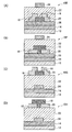
- FIG. 1A is a schematic diagram showing an example of a top contact type TFT having a top gate structure, which is a TFT according to an embodiment of the present invention.
- FIG. 1B is a schematic diagram showing an example of a bottom contact type TFT with a top gate structure, which is a TFT according to an embodiment of the present invention.
- FIG. 1C is a schematic diagram showing an example of a top contact type TFT with a bottom gate structure, which is a TFT according to an embodiment of the present invention.
- FIG. 1D is a schematic diagram showing an example of a bottom contact type TFT with a bottom gate structure, which is a TFT according to an embodiment of the present invention.
- FIG. 1A is a schematic diagram showing an example of a top contact type TFT having a top gate structure, which is a TFT according to an embodiment of the present invention.
- FIG. 1B is a schematic diagram showing an example of a bottom contact type TFT with a top gate structure, which is a TFT according
- FIG. 2A is a schematic diagram showing an example of a top contact type TFT having a top gate structure, which is a TFT according to an embodiment of the present invention.
- FIG. 2B is a schematic diagram showing an example of a bottom contact type TFT with a top gate structure, which is a TFT according to an embodiment of the present invention.
- FIG. 2C is a schematic view showing an example of a top contact type TFT having a bottom gate structure, which is a TFT according to an embodiment of the present invention.
- FIG. 2D is a schematic diagram showing an example of a bottom contact type TFT with a bottom gate structure, which is a TFT according to an embodiment of the present invention.
- FIG. 3A is a schematic diagram showing an example of a top contact type TFT with a top gate structure, which is a TFT according to an embodiment of the present invention.
- FIG. 3B is a schematic diagram showing an example of a bottom contact type TFT with a top gate structure, which is a TFT according to an embodiment of the present invention.
- FIG. 3C is a schematic view showing an example of a top contact type TFT with a bottom gate structure, which is a TFT according to an embodiment of the present invention.
- FIG. 3D is a schematic view showing an example of a bottom contact type TFT with a bottom gate structure, which is a TFT according to an embodiment of the present invention.
- FIG. 3A is a schematic diagram showing an example of a top contact type TFT with a top gate structure, which is a TFT according to an embodiment of the present invention.
- FIG. 3B is a schematic diagram showing an example of a bottom contact type TFT with a top gate structure, which is a TFT according
- FIG. 4 is a schematic sectional view of a part of a liquid crystal display device according to an embodiment of the electro-optical device of the invention.
- FIG. 5 is a schematic configuration diagram of electrical wiring of the liquid crystal display device shown in FIG.
- FIG. 6 is a schematic sectional view of a part of an active matrix type organic EL display device according to an embodiment of the electro-optical device of the invention.
- FIG. 7 is a schematic configuration diagram of the electrical wiring of the electro-optical device shown in FIG.
- FIG. 8 is a schematic sectional view of a part of an X-ray sensor which is an embodiment of the sensor of the present invention.
- FIG. 9 is a schematic configuration diagram of electrical wiring of the sensor shown in FIG.
- FIG. 10A and 10B are diagrams showing the results of measuring a temperature map (substrate temperature 50 ° C.) during element driving, in which FIG. 10A shows a temperature map for a glass substrate, and FIG. 10B shows a temperature for a silicon substrate. Shows the map.
- 15A and 15B are diagrams showing the structure used in the simulation, where FIG. 15A is a perspective view of the structure, and FIG. 15B is a cross-sectional view of the structure.
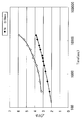
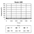
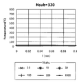
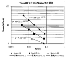
- FIG. 28 is a graph plotting the relationship between N kaku and T for each N sub where T max is 300 ° C., based on the graphs shown in FIGS.
- FIG. 29 is a graph plotting the relationship between N kaku and T for each N sub where T max is 100 ° C., based on the graphs shown in FIGS.
- FIG. 30 is a diagram showing a relationship between N sub at which the maximum heat generation temperature T max is 300 ° C. and the parameter A.
- FIG. 31 is a diagram illustrating a relationship between N sub and the parameter A at which the maximum heat generation temperature T max is 100 ° C.
- a field effect transistor according to an embodiment of the present invention will be specifically described by taking a TFT as an example.
- a TFT according to an embodiment of the present invention includes a gate electrode, a gate insulating film, an active layer, a source electrode, and a drain electrode, and controls a current flowing through the active layer by applying a voltage to the gate electrode. This is an active element having a function of switching a current between drain electrodes.
- the TFT according to the embodiment of the present invention further includes a thermal diffusion layer that is the same as or different from the gate insulating film and is different from the gate electrode, the source electrode, and the drain electrode.
- the element structure of the TFT may be any of a so-called inverted stagger structure (also referred to as a bottom gate type) and a stagger structure (also referred to as a top gate type) based on the position of the gate electrode. Further, based on the contact portion between the active layer and the source and drain electrodes (referred to as “source / drain electrodes” as appropriate), either a so-called top contact type or bottom contact type may be used.
- the top gate type is a form in which a gate electrode is disposed on the upper side of the gate insulating film and an active layer is formed on the lower side of the gate insulating film.
- the bottom gate type is a type on the lower side of the gate insulating film.
- a gate electrode is disposed and an active layer is formed above the gate insulating film.
- the bottom contact type is a mode in which the source / drain electrodes are formed before the active layer and the lower surface of the active layer is in contact with the source / drain electrodes.
- the top contact type is the type in which the active layer is the source / drain. In this embodiment, the upper surface of the active layer is in contact with the source / drain electrodes.
- FIG. 1A is a schematic diagram showing an example of a top contact type TFT having a top gate structure, which is a TFT according to an embodiment of the present invention.
- the thermal diffusion layer 14 and the active layer 16 according to the embodiment of the present invention are sequentially laminated on one main surface of the substrate 12.
- a source electrode 18 and a drain electrode 20 are disposed on the active layer 16 so as to be spaced apart from each other, and a gate insulating film 22 and a gate electrode 24 are sequentially stacked thereon.
- FIG. 1B is a schematic view showing an example of a bottom contact type TFT having a top gate structure, which is a TFT according to an embodiment of the present invention.
- the thermal diffusion layer 14 according to the embodiment of the present invention is laminated on one main surface of the substrate 12, and the source electrode 18 and the drain electrode 20 are connected to each other on the thermal diffusion layer 14. It is set apart.
- the active layer 16, the gate insulating film 22, and the gate electrode 24 are sequentially stacked.
- FIG. 1C is a schematic diagram showing an example of a top contact type TFT having a bottom gate structure, which is a TFT according to an embodiment of the present invention.
- the gate electrode 24, the gate insulating film 22, and the active layer 16 are sequentially stacked on one main surface of the substrate 12.
- a source electrode 18 and a drain electrode 20 are disposed on the surface of the active layer 16 so as to be separated from each other, and the thermal diffusion layer 14 according to the embodiment of the present invention is laminated on the source electrode 18, the drain electrode, and the active layer 16.
- the thermal diffusion layer 14 according to the embodiment of the present invention is laminated on the source electrode 18, the drain electrode, and the active layer 16.
- FIG. 1D is a schematic view showing an example of a bottom contact type TFT with a bottom gate structure, which is a TFT according to an embodiment of the present invention.
- the gate electrode 24 and the gate insulating film 22 are sequentially stacked on one main surface of the substrate 12.
- the source electrode 18 and the drain electrode 20 are disposed on the surface of the gate insulating film 22 so as to be separated from each other, and further on them, the active layer 16 and the thermal diffusion layer 14 according to the embodiment of the present invention, Are sequentially stacked.
- the TFT according to the present embodiment can have various configurations, and may appropriately have a configuration including a protective layer on the active layer, an insulating layer on the substrate, and the like.
- the arrangement of the thermal diffusion layer 14 is preferably directly below or directly above the active layer 16 from the viewpoint of diffusing the heat generated by the active layer 16, and the TFT characteristics are improved.
- the surface on the side opposite to the gate electrode 24 side of the substrate 12 is not particularly limited.
- the active layer 16 may be disposed both above and below the active layer 16.
- at least one thin film having a thickness of 1 ⁇ m or less may be disposed between the active layer 16 and the thermal diffusion layer 14.
- the thermal diffusion layer 14 is separated from the protective layer as a protective layer. It is preferable to arrange on top of. Further, in the bottom gate type oxide TFTs 10 ⁇ / b> C and 10 ⁇ / b> D, the thermal diffusion layer 14 can be disposed between the gate electrode 24 and the substrate 12. Further, the thermal diffusion layer 14 can be provided with the function of the thermal diffusion layer 14 without being arranged separately from the configuration of the gate electrode 24, the gate insulating film 22, and the like. Moreover, the function of the thermal diffusion layer 14 can be given to an interlayer insulating film (not shown) or the insulating film itself.
- FIG. 2A is a schematic diagram showing an example of a top contact type TFT having a top gate structure, which is a TFT according to an embodiment of the present invention.
- the thermal diffusion layer 14, the insulating layer 26, and the active layer 16 according to the embodiment of the present invention are sequentially stacked on one main surface of the substrate 12.
- a source electrode 18 and a drain electrode 20 are disposed on the active layer 16 so as to be spaced apart from each other, and a gate insulating film 22 and a gate electrode 24 are sequentially stacked thereon.
- FIG. 2B is a schematic diagram showing an example of a bottom contact type TFT having a top gate structure, which is a TFT according to an embodiment of the present invention.
- the thermal diffusion layer 14 according to the embodiment of the present invention and the insulating layer 26 are sequentially stacked on one main surface of the substrate 12, and the source electrode 18 is formed on the insulating layer 26.
- the drain electrode 20 are spaced apart from each other.
- the active layer 16, the gate insulating film 22, and the gate electrode 24 are sequentially stacked.
- FIG. 2C is a schematic diagram showing an example of a top contact type TFT having a bottom gate structure, which is a TFT according to an embodiment of the present invention.
- the thermal diffusion layer 14, the gate electrode 24, the gate insulating film 22, and the active layer 16 according to the embodiment of the present invention are sequentially formed on one main surface of the substrate 12.
- a source electrode 18 and a drain electrode 20 are spaced apart from each other on the surface of the active layer 16.
- FIG. 2D is a schematic diagram showing an example of a bottom contact type TFT with a bottom gate structure, which is a TFT according to an embodiment of the present invention.
- the thermal diffusion layer 14, the gate electrode 24, and the gate insulating film 22 according to the embodiment of the present invention are sequentially stacked on one main surface of the substrate 12.
- a source electrode 18 and a drain electrode 20 are disposed on the surface of the gate insulating film 22 so as to be spaced apart from each other, and an active layer 16 is further stacked thereon.
- FIG. 3A is a schematic diagram showing an example of a top contact type TFT with a top gate structure, which is a TFT according to an embodiment of the present invention.
- the active layer 16 is stacked on one main surface of the substrate 12.
- a source electrode 18 and a drain electrode 20 are disposed on the active layer 16 so as to be spaced apart from each other, and a gate insulating film 22, a gate electrode 24, and the thermal diffusion layer 14 according to the embodiment of the present invention. Are stacked in order.
- FIG. 3B is a schematic view showing an example of a bottom contact type TFT having a top gate structure, which is a TFT according to an embodiment of the present invention.
- the source electrode 18 and the drain electrode 20 are provided on one main surface of the substrate 12 so as to be separated from each other. Then, the active layer 16, the gate insulating film 22, the gate electrode 24, and the thermal diffusion layer 14 according to the embodiment of the present invention are sequentially stacked.
- FIG. 3C is a schematic diagram showing an example of a top contact type TFT having a bottom gate structure, which is a TFT according to an embodiment of the present invention.
- the gate electrode 24, the gate insulating film 22, and the active layer 16 are sequentially stacked on one main surface of the substrate 12.
- a source electrode 18 and a drain electrode 20 are spaced apart from each other on the surface of the active layer 16.
- a protective film 28 is stacked on the active layer 16 between the source electrode 18 and the drain electrode 20, and the thermal diffusion layer 14 according to the embodiment of the present invention is formed on the protective film 28, the source electrode 18, and the drain electrode 20.
- the protection of the back channel is considered important for the stability of the TFT, and the protective film 28 is laminated.
- FIG. 3D is a schematic view showing an example of a bottom contact type TFT with a bottom gate structure, which is a TFT according to an embodiment of the present invention.
- the gate electrode 24 and the gate insulating film 22 are sequentially stacked on one main surface of the substrate 12.
- a source electrode 18 and a drain electrode 20 are disposed on the surface of the gate insulating film 22 so as to be spaced apart from each other, and an active layer 16 is further stacked thereon.
- the periphery of the active layer 16 is covered with a protective film 28, and the periphery of the protective film 28 is further covered with the thermal diffusion layer 14 according to the embodiment of the present invention.
- the bottom gate structure it is considered important to protect the back channel for the stability of the TFT, and the active layer 16 is covered with the protective film 28.
- top contact type TFT 10A with the top gate structure shown in FIG. 1A will be specifically described.
- present invention is similarly applied to the case of manufacturing other types of TFTs. can do.
- a substrate 12 for forming the TFT 10A is prepared.
- the structure of the substrate 12 may be a single layer structure or a laminated structure.
- substrate 12 which concerns on embodiment of this invention is a board
- the substrate 12 according to the embodiment of the present invention satisfies the condition of N sub ⁇ 0.56 W / mK.
- the substrate 12 may be doped with the predetermined element.
- a resin substrate and a composite material thereof are preferable in terms of light weight and flexibility.
- the resin substrate is preferably excellent in heat resistance, dimensional stability, solvent resistance, electrical insulation, workability, low air permeability, low moisture absorption, and the like.
- the resin substrate may include a gas barrier layer for preventing permeation of moisture and oxygen, an undercoat layer for improving the flatness of the resin substrate and adhesion with the lower electrode, and the like.
- the thickness of the substrate 12 in the present invention is not particularly limited, but is preferably 50 ⁇ m or more and 1000 ⁇ m or less, and more preferably 50 ⁇ m or more and 500 ⁇ m or less.
- the flatness of the substrate 12 itself is further improved when the thickness of the substrate 12 is 50 ⁇ m or more.
- the thickness of the substrate 12 is 500 ⁇ m or less, the flexibility of the substrate 12 itself is further improved, and the use as a substrate for a flexible device becomes easier.
- the thermal conductivity of the substrate 12 and the thermal diffusion layer 14 can be specified by a measuring method such as a laser flash method, a hot wire method, a flat plate heat flow meter method, or a temperature gradient method.
- the active layer 16 mainly contains an oxide semiconductor containing at least one of In, Ga, and Zn.
- an oxide semiconductor containing at least two of In, Ga, and Zn eg, In—Zn—O, In—Ga—O, and Ga—Zn—O
- In, Ga, and Zn are used.
- An oxide semiconductor containing all of them is more preferable.
- the In—Ga—Zn—O-based oxide semiconductor an oxide semiconductor whose composition in a crystalline state is represented by InGaO 3 (ZnO) m (m is a natural number less than 6) is preferable, and InGaZnO 4 is particularly preferable. .
- the electron mobility tends to increase as the electrical conductivity increases.
- the active layer should just contain the above oxide semiconductors as a main component, and may contain impurities other than that.
- the “main component” represents a component that is contained most among the components constituting the active layer.
- the layer structure of the active layer 16 may be composed of two or more layers.
- the active layer 16 may be either amorphous or crystalline. However, in the case of amorphous, since it can be formed at a low temperature, it is preferably formed on the flexible substrate 12. Whether the active layer 16 is amorphous can be confirmed by X-ray diffraction measurement. That is, when a clear peak indicating a crystal structure is not detected by X-ray diffraction measurement, it can be determined that the active layer 16 is amorphous.
- the film thickness of the active layer 16 is not particularly limited, but is preferably 5 nm or more and 150 nm or less from the viewpoint of thin film flatness and film formation time.
- the film formation method of the active layer 16 is not particularly limited, but a vapor phase film formation method or a solution method (sol-gel, MOD, nanoparticles, CSD, etc.) can be used.
- a vapor phase film formation method or a solution method sol-gel, MOD, nanoparticles, CSD, etc.
- vapor deposition methods sputtering and pulsed laser deposition (PLD) are suitable.
- the sputtering method is preferable from the viewpoint of mass productivity.
- the film is formed by controlling the degree of vacuum and the oxygen flow rate by RF magnetron sputtering deposition.
- the thin film is patterned according to the device.
- Patterning can be performed by photolithography and etching. Specifically, a resist pattern is formed on the remaining portion by photolithography, and the pattern is formed by etching with an acid solution such as hydrochloric acid, nitric acid, dilute sulfuric acid, or a mixed solution of phosphoric acid, nitric acid and acetic acid.
- an acid solution such as hydrochloric acid, nitric acid, dilute sulfuric acid, or a mixed solution of phosphoric acid, nitric acid and acetic acid.
- direct patterning may be performed using an ink jet, a dispenser, or the like without using photolithography.
- thermal diffusion layer 14 is formed on the active layer 16.
- the thermal conductivity N kaku of the thermal diffusion layer 14 is adjusted by adjusting the constituent material and composition ratio of the thermal diffusion layer 14, the film thickness T (mm) of the thermal diffusion layer 14, and the planar aperture ratio R (0 ⁇ 0) of the thermal diffusion layer 14. R ⁇ 1), controlling the crystallinity and the like.
- the constituent material of the thermal diffusion layer 14 is not particularly limited as long as the thermal conductivity N kaku of the thermal diffusion layer 14 satisfies the above conditions, and is a material in which a metal mesh, fine particles, filler, etc. having a high aperture ratio are dispersed. But you can. However, if the electrical conductivity is high, there is a concern about the influence of parasitic capacitance. From the viewpoint of reducing the electrical conductivity to some extent (providing insulation), at least one of Al, Si, Ga, N, O, and C is included. It is a nitride film, and the volume resistivity ⁇ is preferably ⁇ ⁇ 10 2 ⁇ ⁇ cm or more.
- the constituent material of the substrate 12 is glass.
- N sub 1.0 W / mK
- the film thickness T (mm) of the thermal diffusion layer 14 is controlled by controlling the film formation rate by changing the input power, the distance between target substrates, the film formation pressure, etc. in the case of film formation time or sputtering. Can do. That is, in the case of film formation time, the film thickness can be increased by increasing the film formation time, and the film thickness can be decreased by decreasing the film formation time.
- the planar aperture ratio R (0 ⁇ R ⁇ 1) of the thermal diffusion layer 14 can be controlled by lithography or the like.
- the transmittance of the thermal diffusion layer 14 is preferably 70% or more in light having a wavelength range of 400 nm to 700 nm.
- the layer structure of the thermal diffusion layer 14 may be composed of two or more layers.
- the thermal diffusion layer 14 may be either amorphous or crystalline. However, in the case of amorphous, since it can be formed at a low temperature, it is preferably formed on the flexible substrate 12.
- a vapor phase film formation method is used with a polycrystalline sintered body of a nitride film containing at least one of Al, Si, Ga, N, O, and C as a target.
- a vapor deposition method sputtering and pulsed laser deposition (PLD) are suitable.
- PLD pulsed laser deposition
- the sputtering method is preferable from the viewpoint of mass productivity.
- the film is formed by controlling the degree of vacuum and the oxygen flow rate by RF magnetron sputtering deposition.
- the thermal diffusion layer 14 can also use a solution method.
- the thin film is patterned according to the device.
- the patterning is performed before the formation of the active layer 16 in order to remove the influence of interface contamination. It is preferable to pattern simultaneously.
- Source / drain electrodes are used having high conductivity, for example, metals such as Al, Mo, Cr, Ta, Ti, Au, Au, Al—Nd, Ag alloy, tin oxide, zinc oxide, indium oxide, indium oxide.
- a metal oxide conductive film such as tin (ITO) or indium zinc oxide (IZO) can be used.
- ITO tin
- IZO indium zinc oxide
- the source / drain electrodes 18 and 20 are formed by, for example, a wet method such as a printing method or a coating method, a physical method such as a vacuum deposition method, a sputtering method, or an ion plating method, or a chemical method such as CVD or plasma CVD method.
- the film is formed according to a method appropriately selected in consideration of suitability with the material to be used.
- the film thickness of the conductive film to be formed is preferably 10 nm or more and 1000 nm or less, more preferably 50 nm or more and 500 nm or less in consideration of film forming property, patterning property by etching or lift-off method, conductivity, and the like. .
- the formed conductive film is patterned into a predetermined shape by etching or a lift-off method, and source and drain electrodes 18 and 20 are formed. At this time, it is preferable to pattern the wirings connected to the source / drain electrodes 18 and 20 simultaneously.
- the gate insulating film 22 preferably has a high insulating property.
- an insulating film such as SiO 2 , SiNx, SiON, Al 2 O 3 , Y 2 O 3 , Ta 2 O 5 , HfO 2 , or a compound thereof is used.
- An insulating film including at least two or more may be used.
- the gate insulating film 22 is a material used from a wet method such as a printing method or a coating method, a physical method such as a vacuum deposition method, a sputtering method or an ion plating method, or a chemical method such as CVD or plasma CVD method.
- the film is formed according to a method appropriately selected in consideration of the suitability of Next, the gate insulating film 22 is patterned into a predetermined shape by photolithography and etching. Note that the gate insulating film 22 needs to have a thickness for reducing the leakage current and improving the voltage resistance. On the other hand, if the gate insulating film is too thick, the driving voltage is increased.
- the thickness of the gate insulating film is preferably 10 nm to 10 ⁇ m, more preferably 50 nm to 1000 nm, and particularly preferably 100 nm to 400 nm.
- a gate electrode 24 is formed.
- the gate electrode 24 is made of a material having high conductivity, for example, metal such as Al, Mo, Cr, Ta, Ti, Au, Au, Al—Nd, Ag alloy, tin oxide, zinc oxide, indium oxide, indium oxide.
- a metal oxide conductive film such as tin (ITO) or indium zinc oxide (IZO) can be used.
- ITO tin
- IZO indium zinc oxide
- the gate electrode 24 is a material used from, for example, a wet method such as a printing method or a coating method, a physical method such as a vacuum deposition method, a sputtering method, or an ion plating method, or a chemical method such as CVD or plasma CVD method.
- the film is formed according to a method appropriately selected in consideration of the suitability of
- the film thickness of the conductive film to be formed is preferably 10 nm or more and 1000 nm or less, and more preferably 50 nm or more and 500 nm or less in consideration of film forming properties, patterning properties by etching or lift-off methods, conductivity, and the like.
- the conductive film is patterned into a predetermined shape by etching or a lift-off method, and the gate electrode 24 is formed. At this time, it is preferable to pattern the gate electrode 24 and the gate wiring simultaneously.
- the top contact type TFT 10A is manufactured with the top gate structure according to the embodiment of the present invention.
- electro-optical devices for example, display devices such as liquid crystal display devices, organic EL (Electro Luminescence) display devices, inorganic EL display devices, etc.
- a driving element in the above, particularly for a large area device.
- the TFT of this embodiment is particularly suitable for a device that can be manufactured by a low-temperature process using a resin substrate (for example, a flexible display), and various sensors such as an X-ray sensor, MEMS (Micro Electro Mechanical System), and the like. It is suitably used as a drive element (drive circuit) in this electronic device.
- the electro-optical device or sensor includes the above-described TFT of the present invention.
- electro-optical devices include display devices (eg, liquid crystal display devices, organic EL display devices, inorganic EL display devices, etc.).
- an image sensor such as a CCD (Charge Coupled Device) or a CMOS (Complementary Metal Oxide Semiconductor), an X-ray sensor, or the like is suitable.
- the electro-optical device or sensor of the present embodiment exhibits good characteristics with low power consumption.
- the characteristics referred to here indicate display characteristics in the case of an electro-optical device (display device), and sensitivity characteristics in the case of a sensor.
- a liquid crystal display device, an organic EL display device, and an X-ray sensor will be described as representative examples of an electro-optical device or sensor including a thin film transistor manufactured according to the present invention.
- FIG. 4 is a schematic sectional view of a part of a liquid crystal display device according to an embodiment of the electro-optical device of the present invention.
- the liquid crystal display device 100 of the present embodiment has a top gate structure 10A shown in FIG. 1A and a top contact type TFT 10A and a gate electrode 24 protected by the passivation layer 102 of the TFT 10A.
- a liquid crystal layer 108 sandwiched between the pixel lower electrode 104 and the counter upper electrode 106, and an RGB color filter 110 for developing different colors corresponding to each pixel, and the substrate 12 side of the TFT 10A and the RGB color filter 110 are provided. It is the structure provided with polarizing plates 112a and 112b, respectively.
- the liquid crystal display device 100 of this embodiment includes a plurality of gate wirings 112 that are parallel to each other and data wirings 114 that are parallel to each other and intersect the gate wirings 112.
- the gate wiring 112 and the data wiring 114 are electrically insulated.
- a TFT 10A is provided in the vicinity of the intersection of the gate wiring 112 and the data wiring 114.
- the gate electrode 24 of the TFT 10A is connected to the gate wiring 112, and the source electrode 18 of the TFT 10A is connected to the data wiring 114. Further, the drain electrode 20 of the TFT 10A is connected to the pixel lower electrode 104 through a contact hole 116 provided in the gate insulating film 22 (a conductor is embedded in the contact hole 116). The pixel lower electrode 104 forms a capacitor 118 together with the grounded counter upper electrode 106.
- the TFT 10A having the top gate structure is provided in the liquid crystal device of this embodiment shown in FIG. 4, the TFT 10A having the top gate structure is provided.
- the TFT used in the liquid crystal device which is the display device of the present invention is not limited to the top gate structure.
- a TFT having a bottom gate structure may be used.
- the TFT manufactured according to the present invention can reduce heat generation during driving, and has very high stability and reliability, it is suitable for manufacturing a large-screen liquid crystal display device.
- a resin substrate plastic substrate
- a flexible liquid crystal display device having a large area, uniform and stable can be provided.
- FIG. 6 is a schematic sectional view of a part of an active matrix organic EL display device according to an embodiment of the electro-optical device of the present invention
- FIG. 7 is a schematic configuration diagram of electric wiring.
- the simple matrix method has an advantage that it can be manufactured at low cost.
- the number of scanning lines and the light emission time per scanning line are inversely proportional. Therefore, it is difficult to increase the definition and increase the screen size.
- the active matrix method has a high manufacturing cost because a transistor and a capacitor are formed for each pixel.
- it is suitable for high definition and large screen.
- the TFT 10A having the top gate structure shown in FIG. 1A is provided as a driving TFT 204 and a switching TFT 206 on the substrate 12 provided with the passivation layer 202.
- an organic EL light emitting element 214 composed of an organic light emitting layer 212 sandwiched between the lower electrode 208 and the upper electrode 210 is provided on the TFTs 204 and 206, and the upper surface is also protected by the passivation layer 216.
- the organic EL display device 200 of the present embodiment includes a plurality of gate wirings 220 that are parallel to each other, and a data wiring 222 and a driving wiring 224 that are parallel to each other and intersect the gate wiring 220.
- the gate wiring 220, the data wiring 222, and the drive wiring 224 are electrically insulated.
- the gate electrode 24 of the switching TFT 10Ab is connected to the gate wiring 220, and the source electrode 18 of the switching TFT 10Ab is connected to the data wiring 222.
- the drain electrode 20 of the switching TFT 10Ab is connected to the gate electrode 24 of the driving TFT 10A, and the driving TFT 10a is kept on by using the capacitor 226.
- the source electrode 18 of the driving TFT 10 a is connected to the driving wiring 224, and the drain electrode 20 is connected to the organic EL light emitting element 214.
- the organic EL device of this embodiment shown in FIG. 6 includes the top gate TFTs 10a and 10b.
- the TFT used in the organic EL device which is the display device of the present invention is limited to the top gate structure.
- a TFT having a bottom gate structure may be used.
- the TFT manufactured according to the present invention can reduce the heat generation during driving, and thus has very high stability and reliability, and is therefore suitable for manufacturing a large-screen organic EL display device.
- a resin substrate plastic substrate
- a flexible organic EL display device having a large area, uniform and stable can be provided.
- the top electrode 210 may be a top emission type using a transparent electrode, or the bottom electrode 208 and each electrode of a TFT may be a transparent electrode.
- FIG. 8 shows a schematic sectional view of a part of an X-ray sensor which is an embodiment of the sensor of the present invention
- FIG. 9 shows a schematic configuration diagram of its electric wiring.
- FIG. 8 is a schematic cross-sectional view in which a part of the X-ray sensor array is enlarged more specifically.
- the X-ray sensor 300 of this embodiment includes a TFT 10A and a capacitor 310 formed on the substrate 12, a charge collection electrode 302 formed on the capacitor 310, an X-ray conversion layer 304, and an upper electrode 306. Composed.
- a passivation film 308 is provided on the TFT 10A.
- the capacitor 310 has a structure in which an insulating film 316 is sandwiched between a capacitor lower electrode 312 and a capacitor upper electrode 314.
- the capacitor upper electrode 314 is connected to one of the source electrode 18 and the drain electrode 20 (the drain electrode 20 in FIG. 8) of the TFT 10A through a contact hole 318 provided in the insulating film 316.
- the charge collection electrode 302 is provided on the capacitor upper electrode 314 in the capacitor 310 and is in contact with the capacitor upper electrode 314.
- the X-ray conversion layer 304 is a layer made of amorphous selenium, and is provided so as to cover the TFT 10A and the capacitor 310.
- the upper electrode 306 is provided on the X-ray conversion layer 304 and is in contact with the X-ray conversion layer 304.
- the X-ray sensor 300 of this embodiment includes a plurality of gate wirings 320 that are parallel to each other and a plurality of data wirings 322 that intersect with the gate wiring 320 and are parallel to each other.
- the gate wiring 320 and the data wiring 322 are electrically insulated.
- a TFT 10A is provided in the vicinity of the intersection between the gate wiring 320 and the data wiring 322.
- the gate electrode 24 of the TFT 10A is connected to the gate wiring 320, and the source electrode 18 of the TFT 10A is connected to the data wiring 322.
- the drain electrode 20 of the TFT 10 ⁇ / b> A is connected to the charge collecting electrode 302, and the charge collecting electrode 302 is connected to the capacitor 310.
- X-rays are irradiated from the upper part (upper electrode 306 side) in FIG. 8, and electron-hole pairs are generated in the X-ray conversion layer 304.
- the generated charges are accumulated in the capacitor 310 and read out by sequentially scanning the TFT 10A.
- the X-ray sensor 300 according to the present embodiment can reduce heat generation during driving, and thus has high stability and reliability, and thus is suitable for a large screen.
- the active layer 16 is made of IGZO, the mobility is high, so that the sensitivity characteristic is excellent, and an image with a wide dynamic range can be obtained when used in an X-ray digital imaging apparatus.
- the X-ray digital imaging apparatus according to the present embodiment is suitable not only for still image shooting but also for an X-ray digital imaging apparatus that can perform fluoroscopy with a moving image and still image shooting.
- the active layer 16 in the TFT 10A is amorphous, an image with excellent uniformity can be obtained.
- the X-ray sensor of this embodiment shown in FIG. 8 is provided with a TFT having a top gate structure, but the TFT used in the sensor of the present invention is not limited to the top gate structure.
- a TFT having a structure may be used.
- Source (drain) film thickness: 100 nm
- gate electrode was Mo (film thickness: 40 nm)
- insulating layer SiO 2 (film thickness: 200 nm).
- Photolithography and wet etching were used for patterning, oxalic acid was used for etching IGZO, phosphoric acid acetic acid was used for etching the Mo electrode, and buffered hydrofluoric acid was used for etching the insulating layer.
- TSMR9000-LB was used as the resist, and 5% TMAH solution was used as the developer.
- InfraScope II manufactured by Nihon Burns was used.
- FIG. 10A and 10B are diagrams showing the results of measuring a temperature map (substrate temperature 50 ° C.) during element driving, in which FIG. 10A shows a temperature map for a glass substrate, and FIG. 10B shows a temperature for a silicon substrate. Shows the map.
- the threshold shift value indicating the reliability increases as the drive time (heat generation time) becomes longer. And it turns out that the increase in a threshold shift appears notably with the glass substrate with low heat conductivity.
- FIG. 15A and 15B are diagrams showing the structure used in the simulation, where FIG. 15A is a perspective view of the structure, and FIG. 15B is a cross-sectional view of the structure.
- a structure 500 in FIG. 15 has a structure in which a thermal diffusion layer 504, an insulating layer 506, and a heating element 508 are sequentially stacked on a substrate 502.
- parametric analysis was performed to extract the maximum exothermic temperature.
- Boundary condition External boundary condition
- Natural convection ⁇ Mesh size: 0.4
- the conditions for the heating element 508 were as follows. Size: 1 ⁇ 1 ⁇ 0.01mm Thermal conductivity: 10W / mK Calorific value: 0.4W Heat transfer: 20 W / m 2 / deg (heating element / insulating layer boundary condition)
- the conditions for the insulating layer 506 were as follows. Size: 10x10x0.001mm Thermal conductivity: 1W / mK Heat transfer: 15 W / m 2 / deg (insulating layer / thermal diffusion layer boundary condition)
- the conditions for the thermal diffusion layer 504 were as follows. Size: 10 x 10 x Tmm Thermal conductivity: N kaku (W / mK) Heat transfer: 10 W / m 2 / deg (insulating layer / thermal diffusion layer boundary condition)
- the conditions for the substrate 502 were as follows. Size: 10x10x0.5mm Thermal conductivity: N sub (W / mK) Substrate surface temperature: 25 ° C (substrate / external boundary conditions)
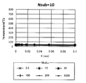
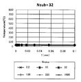
- FIGS. 16 to 27 are diagrams showing the results of simulation, and are graphs showing the relationship (N kaku ⁇ N sub ) with temperature when N sub , N kaku and T are used as parameters.
- the vertical axis plots the maximum value of the heat generation temperature
- the horizontal axis shows the thickness T of the thermal diffusion layer 504.
- the maximum heat generation temperature T max is smaller than 100 ° C. regardless of the value of N kaku . It can also be seen that the maximum exothermic temperature T max is smaller than 300 ° C. when N sub is 0.56 or more. From the above, in the region not applicable to them, the parameters of N sub , N kaku , and T at which the maximum exothermic temperature T max is less than 100 ° C. and less than 300 ° C. are calculated, and the thermal design is performed. The steps are as follows:
- FIG. 30 is a diagram showing a relationship between N sub at which the maximum heat generation temperature T max is 300 ° C. and the parameter A.
- FIG. 31 is a diagram illustrating a relationship between N sub and the parameter A at which the maximum heat generation temperature T max is 100 ° C. (4) From FIG. 30 and FIG. 31, correlation parameters of N kaku , N sub and T can be obtained.
- the region where the maximum heat generation temperature T max is less than 300 ° C. is the heat conduction of the thermal diffusion layer 504 when the thermal conductivity N sub of the substrate 502 satisfies the condition of N sub ⁇ 0.56 W / mK. It has been found that the rate N kaku must satisfy the conditions of N kaku > 0.4 ⁇ S ⁇ ( ⁇ 1.2 ⁇ e ⁇ ( ⁇ 3.5 ⁇ N sub )) and N kaku ⁇ N sub .
- the region where Tmax is less than 100 ° C. is when the thermal conductivity N sub of the substrate 502 satisfies the condition of N sub ⁇ 1.8 W / mK.
- the thermal conductivity N kaku of the thermal diffusion layer 504 needs to satisfy the conditions of N kaku > 3.0 ⁇ S ⁇ ( ⁇ 0.97 ⁇ e ⁇ ( ⁇ 1.2 ⁇ N sub )) and N kaku ⁇ N sub I found out that
- the above formula means a natural logarithm, and “ ⁇ ” means a power.
- “E” in FIG. 28 means “10”.
Landscapes
- Physics & Mathematics (AREA)
- Nonlinear Science (AREA)
- Engineering & Computer Science (AREA)
- Microelectronics & Electronic Packaging (AREA)
- Mathematical Physics (AREA)
- Chemical & Material Sciences (AREA)
- Crystallography & Structural Chemistry (AREA)
- General Physics & Mathematics (AREA)
- Optics & Photonics (AREA)
- Thin Film Transistor (AREA)
- Internal Circuitry In Semiconductor Integrated Circuit Devices (AREA)
Abstract
駆動時の発熱温度を低下させる。基板(12)の熱伝導率をNsub(W/mK)とし、熱拡散層(14)の熱伝導率をNkaku(W/mK)とし、熱拡散層(14)の膜厚をT(mm)とし、熱拡散層(14)の平面開口率をR(0≦R≦1)とし、S=T×Rとしたとき、例えば、基板(12)の熱伝導率Nsubが、Nsub<1.8の条件を満たし、熱拡散層(14)の熱伝導率Nkakuが、Nkaku>3.0×S^(-0.97×e^(-1.2×Nsub))且つNkaku≧Nsubの条件を満たす。
Description
本発明は、電界効果型トランジスタに関する。
電界効果型トランジスタは、半導体メモリ用集積回路の単位素子、高周波信号増幅素子、液晶などの表示素子駆動用素子として広く用いられており、特に薄膜化したものは薄膜トランジスタ(TFT:Thin Film Transistor)と呼ばれている。そして、フラットパネルディスプレイにおいては、大面積で形成可能なアモルファスシリコンからなる活性層を有したシリコン系TFTが用いられている。
近年、このアモルファスシリコンの代わりに、In-Ga-Zn-O系(IGZO系)の酸化物半導体を活性層(チャネル層)に用いたTFTの開発が活発に行われている。酸化物半導体は低温成膜が可能であり、且つアモルファスシリコンよりも高移動度を示し、更に可視光に透明であることからプラスチック板やフィルム等の基板上にフレキシブルで透明なTFTを形成することが可能である。
ところで、このような電界効果型トランジスタにおいて、高電圧印加時(駆動時)に大電流が流れることによりジュール熱が発生し、活性層が局所的に温度上昇することがある。このように駆動時に生じる発熱は、駆動劣化(信頼性の低下)を引き起こす一因となっている。
そこで、特開2003-131588号公報には、駆動時に生じる発熱が蓄熱することを防止するため、薄膜トランジスタの活性層の上層または下層、或いは上下層に放熱層としてガラス基板よりも熱伝導率の高い膜を形成することが開示されている。
しかしながら、特開2003-131588号では、基板の熱伝導率と放熱層の熱伝導率との具体的な関係については一切言及しておらず、ガラス基板よりも熱伝導率の高い膜が、放熱層としての役割を十分に果たしているか否か不明である。
ここで、活性層としてIGZO系の酸化物半導体を用いた場合、発熱時の温度が100℃以上になると基板や活性層、絶縁膜、電極内に存在する微量の水分に影響を与え、所謂TFT特性を変化させてしまう。また、発熱時の温度が300℃以上になると活性層内に存在する酸素が変化し、TFT特性を変化させてしまう。
また、樹脂基板を用いたフレキシブルデバイスの作製においては、基板の熱伝導率がより低くなるため蓄熱し易くなり発熱による駆動劣化がより顕著になると予想される。また、このような発熱の効果は、耐熱性の低い樹脂基板では、蓄熱による基板の寸法変化等を引き起こす原因となることが考えられる。
また、樹脂基板を用いたフレキシブルデバイスの作製においては、基板の熱伝導率がより低くなるため蓄熱し易くなり発熱による駆動劣化がより顕著になると予想される。また、このような発熱の効果は、耐熱性の低い樹脂基板では、蓄熱による基板の寸法変化等を引き起こす原因となることが考えられる。
しかしながら、特開2003-131588号では、上記の点についても、一切言及していない。
本発明は上記事実に鑑みてなされたものであり、駆動時の発熱温度を低下させた電界効果型トランジスタを提供することを目的とする。
<1>基板上に、少なくともゲート電極、ゲート絶縁膜、In,Ga,Znのうち少なくとも一つを含んだ酸化物半導体を主に含有する活性層、ソース電極、及びドレイン電極を有する電界効果型トランジスタであって、前記ゲート絶縁膜と同一又は別個とされ、且つ、前記ゲート電極、ソース電極及びドレイン電極とは異なる熱拡散層を有し、前記基板の熱伝導率をNsub(W/mK)とし、前記熱拡散層の熱伝導率をNkaku(W/mK)とし、前記熱拡散層の膜厚をT(mm)とし、前記熱拡散層の平面開口率をR(0≦R≦1)とし、S=T×Rとしたとき、前記基板の熱伝導率Nsubが、Nsub<1.8の条件を満たし、前記熱拡散層の熱伝導率Nkakuが、Nkaku>3.0×S^(-0.97×e^(-1.2×Nsub))且つNkaku≧Nsubの条件を満たす、電界効果型トランジスタ。
<2>基板上に、少なくともゲート電極、ゲート絶縁膜、In,Ga,Znのうち少なくとも一つを含んだ酸化物半導体を主に含有する活性層、ソース電極、及びドレイン電極を有する電界効果型トランジスタであって、前記ゲート絶縁膜と同一又は別個とされ、且つ、前記ゲート電極、ソース電極及びドレイン電極とは異なる熱拡散層を有し、前記基板の熱伝導率をNsub(W/mK)とし、前記熱拡散層の熱伝導率をNkaku(W/mK)とし、前記熱拡散層の膜厚をT(mm)とし、前記熱拡散層の平面開口率をR(0≦R≦1)とし、S=T×Rとしたとき、前記基板の熱伝導率Nsubが、Nsub<0.56の条件を満たし、前記熱拡散層の熱伝導率Nkakuが、Nkaku>0.4×S^(-1.2×e^(-3.5×Nsub))及びNkaku≧Nsubの条件を満たす、電界効果型トランジスタ。
<3>前記活性層と前記熱拡散層の間に1μm以下の薄膜が少なくとも1層以上存在する、<1>又は<2>に記載の電界効果型トランジスタ。
<4>前記熱拡散層が、Al,Gaの少なくとも一つを含む窒化膜である、<3>に記載の電界効果型トランジスタ。
<5>前記熱拡散層の透過率が、波長域400nm以上700nm以下の光において70%以上である、<4>に記載の電界効果型トランジスタ。
<6>前記基板は、樹脂基板である、<1>~<5>の何れか1つに記載の電界効果型トランジスタ。
<7><6>に記載の電界効果型トランジスタを備えた表示装置。
<8><6>に記載の電界効果型トランジスタを備えたセンサ。
なお、上記「e」は、自然対数を意味し、「^」は、累乗を意味するものとする。
<2>基板上に、少なくともゲート電極、ゲート絶縁膜、In,Ga,Znのうち少なくとも一つを含んだ酸化物半導体を主に含有する活性層、ソース電極、及びドレイン電極を有する電界効果型トランジスタであって、前記ゲート絶縁膜と同一又は別個とされ、且つ、前記ゲート電極、ソース電極及びドレイン電極とは異なる熱拡散層を有し、前記基板の熱伝導率をNsub(W/mK)とし、前記熱拡散層の熱伝導率をNkaku(W/mK)とし、前記熱拡散層の膜厚をT(mm)とし、前記熱拡散層の平面開口率をR(0≦R≦1)とし、S=T×Rとしたとき、前記基板の熱伝導率Nsubが、Nsub<0.56の条件を満たし、前記熱拡散層の熱伝導率Nkakuが、Nkaku>0.4×S^(-1.2×e^(-3.5×Nsub))及びNkaku≧Nsubの条件を満たす、電界効果型トランジスタ。
<3>前記活性層と前記熱拡散層の間に1μm以下の薄膜が少なくとも1層以上存在する、<1>又は<2>に記載の電界効果型トランジスタ。
<4>前記熱拡散層が、Al,Gaの少なくとも一つを含む窒化膜である、<3>に記載の電界効果型トランジスタ。
<5>前記熱拡散層の透過率が、波長域400nm以上700nm以下の光において70%以上である、<4>に記載の電界効果型トランジスタ。
<6>前記基板は、樹脂基板である、<1>~<5>の何れか1つに記載の電界効果型トランジスタ。
<7><6>に記載の電界効果型トランジスタを備えた表示装置。
<8><6>に記載の電界効果型トランジスタを備えたセンサ。
なお、上記「e」は、自然対数を意味し、「^」は、累乗を意味するものとする。
本発明によれば、駆動時の発熱温度を低下させた電界効果型トランジスタを提供することができる。
以下、添付の図面を参照しながら、本発明の実施形態に係る電界効果型トランジスタ、表示装置、センサについて具体的に説明する。なお、図中、同一又は対応する機能を有する部材(構成要素)には同じ符号を付して適宜説明を省略する。
1.電界効果型トランジスタ
本発明の実施形態に係る電界効果型トランジスタについて、TFTを一例に挙げて具体的に説明する。
本発明の実施形態に係る電界効果型トランジスタについて、TFTを一例に挙げて具体的に説明する。
<TFTの概略構成>
本発明の実施形態に係るTFTは、ゲート電極、ゲート絶縁膜、活性層、ソース電極及びドレイン電極を有し、ゲート電極に電圧を印加して、活性層に流れる電流を制御し、ソース電極とドレイン電極間の電流をスイッチングする機能を有するアクテイブ素子である。そして、本発明の実施形態に係るTFTではさらに、ゲート絶縁膜と同一又は別個とされ、且つ、ゲート電極、ソース電極及びドレイン電極とは異なる熱拡散層を有している。
本発明の実施形態に係るTFTは、ゲート電極、ゲート絶縁膜、活性層、ソース電極及びドレイン電極を有し、ゲート電極に電圧を印加して、活性層に流れる電流を制御し、ソース電極とドレイン電極間の電流をスイッチングする機能を有するアクテイブ素子である。そして、本発明の実施形態に係るTFTではさらに、ゲート絶縁膜と同一又は別個とされ、且つ、ゲート電極、ソース電極及びドレイン電極とは異なる熱拡散層を有している。
TFTの素子構造としては、ゲート電極の位置に基づいた、いわゆる逆スタガ構造(ボトムゲート型とも呼ばれる)及びスタガ構造(トップゲート型とも呼ばれる)のいずれの態様であってもよい。また、活性層とソース電極及びドレイン電極(適宜、「ソース・ドレイン電極」という。)との接触部分に基づき、いわゆるトップコンタクト型、ボトムコンタクト型のいずれの態様であってもよい。
なお、トップゲート型とは、ゲート絶縁膜の上側にゲート電極が配置され、ゲート絶縁膜の下側に活性層が形成された形態であり、ボトムゲート型とは、ゲート絶縁膜の下側にゲート電極が配置され、ゲート絶縁膜の上側に活性層が形成された形態である。また、ボトムコンタクト型とは、ソース・ドレイン電極が活性層よりも先に形成されて活性層の下面がソース・ドレイン電極に接触する形態であり、トップコンタクト型とは、活性層がソース・ドレイン電極よりも先に形成されて活性層の上面がソース・ドレイン電極に接触する形態である。
なお、トップゲート型とは、ゲート絶縁膜の上側にゲート電極が配置され、ゲート絶縁膜の下側に活性層が形成された形態であり、ボトムゲート型とは、ゲート絶縁膜の下側にゲート電極が配置され、ゲート絶縁膜の上側に活性層が形成された形態である。また、ボトムコンタクト型とは、ソース・ドレイン電極が活性層よりも先に形成されて活性層の下面がソース・ドレイン電極に接触する形態であり、トップコンタクト型とは、活性層がソース・ドレイン電極よりも先に形成されて活性層の上面がソース・ドレイン電極に接触する形態である。
図1(A)は、本発明の実施形態に係るTFTであって、トップゲート構造でトップコンタクト型のTFTの一例を示す模式図である。図1(A)に示すTFT10Aでは、基板12の一方の主面上に本発明の実施形態に係る熱拡散層14と、活性層16とが、順に積層されている。そして、この活性層16上にソース電極18及びドレイン電極20が互いに離間して設置され、更にこれらの上にゲート絶縁膜22と、ゲート電極24とが順に積層されている。
図1(B)は、本発明の実施形態に係るTFTであって、トップゲート構造でボトムコンタクト型のTFTの一例を示す模式図である。図1(B)に示すTFT10Bでは、基板12の一方の主面上に本発明の実施形態に係る熱拡散層14が積層され、この熱拡散層14上にソース電極18及びドレイン電極20が互いに離間して設置されている。そして、活性層16と、ゲート絶縁膜22と、ゲート電極24と、が順に積層されている。
図1(C)は、本発明の実施形態に係るTFTであって、ボトムゲート構造でトップコンタクト型のTFTの一例を示す模式図である。図1(C)に示すTFT10Cでは、基板12の一方の主面上にゲート電極24と、ゲート絶縁膜22と、活性層16と、が順に積層されている。そして、この活性層16の表面上にソース電極18及びドレイン電極20が互いに離間して設置され、ソース電極18やドレイン電極、活性層16上に本発明の実施形態に係る熱拡散層14が積層されている。
図1(D)は、本発明の実施形態に係るTFTであって、ボトムゲート構造でボトムコンタクト型のTFTの一例を示す模式図である。図1(D)に示すTFT10Dでは、基板12の一方の主面上にゲート電極24と、ゲート絶縁膜22と、が順に積層されている。そして、このゲート絶縁膜22の表面上にソース電極18及びドレイン電極20が互いに離間して設置され、更にこれらの上に、活性層16と、本発明の実施形態に係る熱拡散層14と、が順に積層されている。
なお、本実施形態に係るTFTは、上記以外にも、様々な構成をとることが可能であり、適宜、活性層上に保護層や基板上に絶縁層等を備える構成であってもよい。
熱拡散層14の配置は、図1(A)~(D)に示すように、活性層16の発熱を拡散するという観点から活性層16の直下又は直上であることが好ましく、TFTの特性に影響を与えてしまうことから、活性層とゲート絶縁膜の界面と反対側に設置されることがより好ましいが、特に限定されることはなく、基板12のゲート電極24側とは反対側の面に配置してもよく、また、活性層16を挟んで上下両方に配置してもよい。また、活性層16と熱拡散層14の間に1μm以下の薄膜をすくなくとも1層以上配置するようにしてもよい。例えば、ボトムゲート型酸化物TFT10C,10Dにおいては、活性層16の上部に配置される不図示の保護層が駆動安定化に重要であるため、熱拡散層14は保護層とは別個として保護層の上に配置することが好ましい。また、ボトムゲート型酸化物TFT10C,10Dにおいて、ゲート電極24と基板12との間に、熱拡散層14を配置することもできる。
また、熱拡散層14をゲート電極24やゲート絶縁膜22等の構成とは別個に配置せず、ゲート絶縁膜22自体に熱拡散層14の機能を持たせることもできる。また、不図示の層間絶縁膜や絶縁膜自体に熱拡散層14の機能を持たせることもできる。
熱拡散層14の配置は、図1(A)~(D)に示すように、活性層16の発熱を拡散するという観点から活性層16の直下又は直上であることが好ましく、TFTの特性に影響を与えてしまうことから、活性層とゲート絶縁膜の界面と反対側に設置されることがより好ましいが、特に限定されることはなく、基板12のゲート電極24側とは反対側の面に配置してもよく、また、活性層16を挟んで上下両方に配置してもよい。また、活性層16と熱拡散層14の間に1μm以下の薄膜をすくなくとも1層以上配置するようにしてもよい。例えば、ボトムゲート型酸化物TFT10C,10Dにおいては、活性層16の上部に配置される不図示の保護層が駆動安定化に重要であるため、熱拡散層14は保護層とは別個として保護層の上に配置することが好ましい。また、ボトムゲート型酸化物TFT10C,10Dにおいて、ゲート電極24と基板12との間に、熱拡散層14を配置することもできる。
また、熱拡散層14をゲート電極24やゲート絶縁膜22等の構成とは別個に配置せず、ゲート絶縁膜22自体に熱拡散層14の機能を持たせることもできる。また、不図示の層間絶縁膜や絶縁膜自体に熱拡散層14の機能を持たせることもできる。
以下、活性層16と熱拡散層14の間に1μm以下の薄膜を活性層16の下方に1層配置する場合の一例を挙げる。
図2(A)は、本発明の実施形態に係るTFTであって、トップゲート構造でトップコンタクト型のTFTの一例を示す模式図である。図2(A)に示すTFT10Eでは、基板12の一方の主面上に本発明の実施形態に係る熱拡散層14と、絶縁層26と、活性層16とが、順に積層されている。そして、この活性層16上にソース電極18及びドレイン電極20が互いに離間して設置され、更にこれらの上にゲート絶縁膜22と、ゲート電極24とが順に積層されている。
図2(A)は、本発明の実施形態に係るTFTであって、トップゲート構造でトップコンタクト型のTFTの一例を示す模式図である。図2(A)に示すTFT10Eでは、基板12の一方の主面上に本発明の実施形態に係る熱拡散層14と、絶縁層26と、活性層16とが、順に積層されている。そして、この活性層16上にソース電極18及びドレイン電極20が互いに離間して設置され、更にこれらの上にゲート絶縁膜22と、ゲート電極24とが順に積層されている。
図2(B)は、本発明の実施形態に係るTFTであって、トップゲート構造でボトムコンタクト型のTFTの一例を示す模式図である。図2(B)に示すTFT10Fでは、基板12の一方の主面上に本発明の実施形態に係る熱拡散層14と、絶縁層26とが順に積層され、この絶縁層26上にソース電極18及びドレイン電極20が互いに離間して設置されている。そして、活性層16と、ゲート絶縁膜22と、ゲート電極24と、が順に積層されている。
図2(C)は、本発明の実施形態に係るTFTであって、ボトムゲート構造でトップコンタクト型のTFTの一例を示す模式図である。図2(C)に示すTFT10Gでは、基板12の一方の主面上に本発明の実施形態に係る熱拡散層14と、ゲート電極24と、ゲート絶縁膜22と、活性層16と、が順に積層されている。そして、この活性層16の表面上にソース電極18及びドレイン電極20が互いに離間して設置されている。
図2(D)は、本発明の実施形態に係るTFTであって、ボトムゲート構造でボトムコンタクト型のTFTの一例を示す模式図である。図2(D)に示すTFT10Hでは、基板12の一方の主面上に本発明の実施形態に係る熱拡散層14と、ゲート電極24と、ゲート絶縁膜22と、が順に積層されている。そして、このゲート絶縁膜22の表面上にソース電極18及びドレイン電極20が互いに離間して設置され、更にこれらの上に、活性層16が積層されている。
次に、活性層16と熱拡散層14の間に1μm以下の薄膜を活性層16の上方に1層配置する場合の一例を挙げる。
図3(A)は、本発明の実施形態に係るTFTであって、トップゲート構造でトップコンタクト型のTFTの一例を示す模式図である。図3(A)に示すTFT10Iでは、基板12の一方の主面上に活性層16が積層されている。そして、この活性層16上にソース電極18及びドレイン電極20が互いに離間して設置され、更にこれらの上にゲート絶縁膜22と、ゲート電極24と、本発明の実施形態に係る熱拡散層14と、が順に積層されている。
図3(A)は、本発明の実施形態に係るTFTであって、トップゲート構造でトップコンタクト型のTFTの一例を示す模式図である。図3(A)に示すTFT10Iでは、基板12の一方の主面上に活性層16が積層されている。そして、この活性層16上にソース電極18及びドレイン電極20が互いに離間して設置され、更にこれらの上にゲート絶縁膜22と、ゲート電極24と、本発明の実施形態に係る熱拡散層14と、が順に積層されている。
図3(B)は、本発明の実施形態に係るTFTであって、トップゲート構造でボトムコンタクト型のTFTの一例を示す模式図である。図3(B)に示すTFT10Jでは、基板12の一方の主面上にソース電極18及びドレイン電極20が互いに離間して設置されている。そして、活性層16と、ゲート絶縁膜22と、ゲート電極24と、本発明の実施形態に係る熱拡散層14と、が順に積層されている。
図3(C)は、本発明の実施形態に係るTFTであって、ボトムゲート構造でトップコンタクト型のTFTの一例を示す模式図である。図3(C)に示すTFT10Kでは、基板12の一方の主面上にゲート電極24と、ゲート絶縁膜22と、活性層16と、が順に積層されている。そして、この活性層16の表面上にソース電極18及びドレイン電極20が互いに離間して設置されている。そして、ソース電極18及びドレイン電極20の間で活性層16上には保護膜28が積層され、保護膜28やソース電極18、ドレイン電極20上には本発明の実施形態に係る熱拡散層14が積層されている。なお、ボトムゲート構造の場合には、TFTの安定性のためにバックチャネルの保護が重要と考え、保護膜28を積層している。
図3(D)は、本発明の実施形態に係るTFTであって、ボトムゲート構造でボトムコンタクト型のTFTの一例を示す模式図である。図3(D)に示すTFT10Lでは、基板12の一方の主面上にゲート電極24と、ゲート絶縁膜22と、が順に積層されている。そして、このゲート絶縁膜22の表面上にソース電極18及びドレイン電極20が互いに離間して設置され、更にこれらの上に、活性層16が積層されている。活性層16の周囲は保護膜28で覆われており、保護膜28の周囲はさらに、本発明の実施形態に係る熱拡散層14で覆われている。なお、ボトムゲート構造の場合には、TFTの安定性のためにバックチャネルの保護が重要と考え、活性層16を保護膜28で覆っている。
以下、各構成要素について詳述する。なお、代表例として図1(A)に示すトップゲート構造でトップコンタクト型のTFT10Aを製造する場合について具体的に説明するが、本発明は他の形態のTFTを製造する場合についても同様に適用することができる。
<TFTの詳細構成>
-基板-
まず、TFT10Aを形成するための基板12を用意する。基板12の形状、構造、大きさ等については特に制限はなく、目的に応じて適宜選択することが出来る。基板12の構造は単層構造であってもよいし、積層構造であってもよい。
そして、本発明の実施形態に係る基板12は、熱伝導率の低い基板であり、この熱伝導率をNsub(W/mK)としたとき、熱伝導率Nsubが、Nsub<1.8W/mKの条件を満たしている。この条件を満たすと、駆動条件がVg=20V、Vds=50Vである場合の駆動時の発熱温度(最大温度)が100℃以上となってしまい、駆動時の発熱温度を100℃未満に低下させる特別な構成(熱拡散層14の導入)を特に必要とするからである。
又は、本発明の実施形態に係る基板12は、Nsub<0.56W/mKの条件を満たしている。この条件を満たすと、駆動条件がVg=20V、Vds=50Vである場合の駆動時の発熱温度(最大温度)が300℃以上となってしまい、駆動時の発熱温度を300℃未満に低下させる特別な構成(熱拡散層14の導入)を特に必要とするからである。
-基板-
まず、TFT10Aを形成するための基板12を用意する。基板12の形状、構造、大きさ等については特に制限はなく、目的に応じて適宜選択することが出来る。基板12の構造は単層構造であってもよいし、積層構造であってもよい。
そして、本発明の実施形態に係る基板12は、熱伝導率の低い基板であり、この熱伝導率をNsub(W/mK)としたとき、熱伝導率Nsubが、Nsub<1.8W/mKの条件を満たしている。この条件を満たすと、駆動条件がVg=20V、Vds=50Vである場合の駆動時の発熱温度(最大温度)が100℃以上となってしまい、駆動時の発熱温度を100℃未満に低下させる特別な構成(熱拡散層14の導入)を特に必要とするからである。
又は、本発明の実施形態に係る基板12は、Nsub<0.56W/mKの条件を満たしている。この条件を満たすと、駆動条件がVg=20V、Vds=50Vである場合の駆動時の発熱温度(最大温度)が300℃以上となってしまい、駆動時の発熱温度を300℃未満に低下させる特別な構成(熱拡散層14の導入)を特に必要とするからである。
基板12の材質としては、Nsub<1.8W/mK、又はNsub<0.56W/mKの条件を満たしていれば、特に限定はなく、また材質自体がsub<1.8W/mK、又はNsub<0.56W/mKの条件を満たさない場合でも、所定の元素を基板12にドープして満たすようにしてもよい。
例えば、ガラス(Nsub=1.0W/mK)、YSZ(イットリウム安定化ジルコニウム)(Nsub=1.4W/mK)等の無機基板、樹脂基板や、その複合材料等を用いることが出来る。中でも軽量である点、可撓性を有する点から樹脂基板やその複合材料が好ましい。一部熱伝導率の記載は省略するものの具体的には、ポリブチレンテレフタレート(Nsub=0.21~0.25W/mK)、ポリエチレンテレフタレート(Nsub=0.20~0.33W/mK)、ポリエチレンナフタレート(Nsub=0.20~0.33W/mK)、ポリブチレンナフタレート、ポリスチレン(Nsub=0.108W/mK)、ポリカーボネート(Nsub=0.19W/mK)、ポリスルホン、ポリエーテルスルホン(Nsub=0.32W/mK)、ポリアリレート(Nsub=0.24W/mK)、アリルジグリコールカーボネート、ポリアミド(Nsub=0.24W/mK)、ポリイミド(Nsub=0.28~0.34W/mK) 、ポリアミドイミド(Nsub=0.38W/mk)、ポリエーテルイミド(Nsub=0.22W/mK)、ポリベンザアゾール(Nsub=0.23W/mk)、ポリフェニレンサルファイド、ポリシクロオレフィン、ノルボルネン樹脂、ポリクロロトリフルオロエチレン(Nsub=0.20~0.22W/mK)等のフッ素樹脂、液晶ポリマー、アクリル樹脂(Nsub=0.21W/mK)、エポキシ樹脂(Nsub=0.17~0.21W/mK)、シリコン樹脂(Nsub=0.15~0.17W/mK)、アイオノマー樹脂、シアネート樹脂、架橋フマル酸ジエステル、環状ポリオレフィン、芳香族エーテル、マレイミドーオレフィン、セルロース、エピスルフィド化合物等の合成樹脂基板、酸化珪素粒子との複合プラスチック材料、金属ナノ粒子、無機酸化物ナノ粒子、無機窒化物ナノ粒子等との複合プラスチック材料、カーボン繊維、カーボンナノチューブとの複合プラスチック材料、ガラスフェレーク、ガラスファイバー、ガラスビーズとの複合プラスチック材料、粘土鉱物や雲母派生結晶構造を有する粒子との複合プラスチック材料、薄いガラスと上記単独有機材料との間に少なくとも1回の接合界面を有する積層プラスチック材料、無機層と有機層を交互に積層することで、少なくとも1回以上の接合界面を有するバリア性能を有する複合材料、ステンレス基板或いはステンレスと異種金属を積層した金属多層基板、アルミニウム基板或いは表面に酸化処理(例えば陽極酸化処理)を施すことで表面の絶縁性を向上させた酸化皮膜付きのアルミニウム基板等を用いることが出来る。
基板12が、特に樹脂基板である場合は、Nsub<1.8W/mK、又はNsub<0.56W/mKの条件を満たし易く、駆動条件がVg=20V、Vds=50Vである場合の駆動時の発熱温度(最大温度)が100℃以上又は300℃以上となってしまい、駆動時の発熱温度を100℃未満又は300℃未満に低下させる特別な構成(熱拡散層14の導入)を特に必要とする。
また、樹脂基板は、耐熱性、寸法安定性、耐溶剤性、電気絶縁性、加工性、低通気性、又は低吸湿性等に優れていることが好ましい。前記樹脂基板は、水分や酸素の透過を防止するためのガスバリア層や、樹脂基板の平坦性や下部電極との密着性を向上するためのアンダーコート層等を備えていてもよい。
例えば、ガラス(Nsub=1.0W/mK)、YSZ(イットリウム安定化ジルコニウム)(Nsub=1.4W/mK)等の無機基板、樹脂基板や、その複合材料等を用いることが出来る。中でも軽量である点、可撓性を有する点から樹脂基板やその複合材料が好ましい。一部熱伝導率の記載は省略するものの具体的には、ポリブチレンテレフタレート(Nsub=0.21~0.25W/mK)、ポリエチレンテレフタレート(Nsub=0.20~0.33W/mK)、ポリエチレンナフタレート(Nsub=0.20~0.33W/mK)、ポリブチレンナフタレート、ポリスチレン(Nsub=0.108W/mK)、ポリカーボネート(Nsub=0.19W/mK)、ポリスルホン、ポリエーテルスルホン(Nsub=0.32W/mK)、ポリアリレート(Nsub=0.24W/mK)、アリルジグリコールカーボネート、ポリアミド(Nsub=0.24W/mK)、ポリイミド(Nsub=0.28~0.34W/mK) 、ポリアミドイミド(Nsub=0.38W/mk)、ポリエーテルイミド(Nsub=0.22W/mK)、ポリベンザアゾール(Nsub=0.23W/mk)、ポリフェニレンサルファイド、ポリシクロオレフィン、ノルボルネン樹脂、ポリクロロトリフルオロエチレン(Nsub=0.20~0.22W/mK)等のフッ素樹脂、液晶ポリマー、アクリル樹脂(Nsub=0.21W/mK)、エポキシ樹脂(Nsub=0.17~0.21W/mK)、シリコン樹脂(Nsub=0.15~0.17W/mK)、アイオノマー樹脂、シアネート樹脂、架橋フマル酸ジエステル、環状ポリオレフィン、芳香族エーテル、マレイミドーオレフィン、セルロース、エピスルフィド化合物等の合成樹脂基板、酸化珪素粒子との複合プラスチック材料、金属ナノ粒子、無機酸化物ナノ粒子、無機窒化物ナノ粒子等との複合プラスチック材料、カーボン繊維、カーボンナノチューブとの複合プラスチック材料、ガラスフェレーク、ガラスファイバー、ガラスビーズとの複合プラスチック材料、粘土鉱物や雲母派生結晶構造を有する粒子との複合プラスチック材料、薄いガラスと上記単独有機材料との間に少なくとも1回の接合界面を有する積層プラスチック材料、無機層と有機層を交互に積層することで、少なくとも1回以上の接合界面を有するバリア性能を有する複合材料、ステンレス基板或いはステンレスと異種金属を積層した金属多層基板、アルミニウム基板或いは表面に酸化処理(例えば陽極酸化処理)を施すことで表面の絶縁性を向上させた酸化皮膜付きのアルミニウム基板等を用いることが出来る。
基板12が、特に樹脂基板である場合は、Nsub<1.8W/mK、又はNsub<0.56W/mKの条件を満たし易く、駆動条件がVg=20V、Vds=50Vである場合の駆動時の発熱温度(最大温度)が100℃以上又は300℃以上となってしまい、駆動時の発熱温度を100℃未満又は300℃未満に低下させる特別な構成(熱拡散層14の導入)を特に必要とする。
また、樹脂基板は、耐熱性、寸法安定性、耐溶剤性、電気絶縁性、加工性、低通気性、又は低吸湿性等に優れていることが好ましい。前記樹脂基板は、水分や酸素の透過を防止するためのガスバリア層や、樹脂基板の平坦性や下部電極との密着性を向上するためのアンダーコート層等を備えていてもよい。
また、本発明における基板12の厚みに特に制限はないが、50μm以上1000μm以下が好ましく、50μm以上500μm以下であることがより好ましい。 基板12の厚みが50μm以上であると、基板12自体の平坦性がより向上する。また、基板12の厚みが500μm以下であると、基板12自体の可撓性がより向上し、フレキシブルデバイス用基板としての使用がより容易となる。
なお、本実施形態で、基板12や熱拡散層14の熱伝導率は、レーザーフラッシュ法、 熱線法、平板熱流計法、又は温度傾斜法等の測定方法によって特定することができる。
-活性層-
次に、基板12上に、活性層16を形成する。(溶液法の記載もお願いいたします)
活性層16は、In,Ga,Znのうち少なくとも一種を含んだ酸化物半導体を主に含有している。特に、In,Ga,Znのうちの少なくとも2種を含む酸化物半導体(例えばIn-Zn-O系、In-Ga-O系、Ga-Zn-O系)が好ましく、In,Ga,Znを全て含む酸化物半導体がより好ましい。In-Ga-Zn-O系酸化物半導体としては、結晶状態における組成がInGaO3(ZnO)m(mは6未満の自然数)で表される酸化物半導体が好ましく、特に、InGaZnO4がより好ましい。この組成の酸化物半導体の特徴としては、電気伝導度が増加するにつれ、電子移動度が増加する傾向を示す。
ただし、IGZOの組成比は、厳密にIn:Ga:Zn=1:1:1となる必要はない。また、活性層は、上記のような酸化物半導体を主成分として含有していれば良く、その他に不純物等を含有していても良い。ここで、「主成分」とは、活性層を構成する構成成分のうち、最も多く含有される成分を表す。
次に、基板12上に、活性層16を形成する。(溶液法の記載もお願いいたします)
活性層16は、In,Ga,Znのうち少なくとも一種を含んだ酸化物半導体を主に含有している。特に、In,Ga,Znのうちの少なくとも2種を含む酸化物半導体(例えばIn-Zn-O系、In-Ga-O系、Ga-Zn-O系)が好ましく、In,Ga,Znを全て含む酸化物半導体がより好ましい。In-Ga-Zn-O系酸化物半導体としては、結晶状態における組成がInGaO3(ZnO)m(mは6未満の自然数)で表される酸化物半導体が好ましく、特に、InGaZnO4がより好ましい。この組成の酸化物半導体の特徴としては、電気伝導度が増加するにつれ、電子移動度が増加する傾向を示す。
ただし、IGZOの組成比は、厳密にIn:Ga:Zn=1:1:1となる必要はない。また、活性層は、上記のような酸化物半導体を主成分として含有していれば良く、その他に不純物等を含有していても良い。ここで、「主成分」とは、活性層を構成する構成成分のうち、最も多く含有される成分を表す。
なお、活性層16の層構造は、2層以上から構成されていてもよい。
また、活性層16は、非晶質又は結晶質のいずれであってもよい。ただし、非晶質の場合には、低温で成膜可能であるために、可撓性のある基板12上に好適に形成される。なお、活性層16が非晶質であるかどうかは、X線回折測定により確認することができる。即ち、X線回折測定により、結晶構造を示す明確なピークが検出されなかった場合は、その活性層16は非晶質であると判断することができる。
また、活性層16は、非晶質又は結晶質のいずれであってもよい。ただし、非晶質の場合には、低温で成膜可能であるために、可撓性のある基板12上に好適に形成される。なお、活性層16が非晶質であるかどうかは、X線回折測定により確認することができる。即ち、X線回折測定により、結晶構造を示す明確なピークが検出されなかった場合は、その活性層16は非晶質であると判断することができる。
活性層16の膜厚は、特に限定されないが、薄膜の平坦性及び成膜時間の観点から5nm以上150nm以下であることが好ましい。
活性層16の成膜方法としては、特に限定されないが、気相成膜法や溶液法(ゾルゲル、MOD、ナノ粒子、CSD等)を用いることができる。中でも大面積の成膜が容易という観点から、In,Ga,Znのうち少なくとも一種を含んだ酸化物半導体の多結晶焼結体をターゲットとして、気相成膜法を用いるのが好ましい。気相成膜法の中でも、スパッタリング法、パルスレーザー蒸着法(PLD法)が適している。さらに、量産性の観点から、スパッタリング法が好ましい。例えば、RFマグネトロンスパッタリング蒸着法により、真空度及び酸素流量を制御して成膜される。
活性層16の成膜後は、デバイスに応じて当該薄膜をパターンニングする。パターンニングはフォトリソグラフィー及びエッチングにより行うことが出来る。具体的には、残存させる部分にフォトリソグラフィーによりレジストパターンを形成し、塩酸、硝酸、希硫酸、又は燐酸、硝酸及び酢酸の混合液等の酸溶液によりエッチングすることによりパターンを形成する。なお、溶液法の場合は、フォトリソグラフィーなどを用いずにインクジェットやディスペンサー等を用いて直接パターニングをしてもよい。
-熱拡散層-
活性層16上には、熱拡散層14を形成する。この熱拡散層14は、以下の条件を満たす。
すなわち、熱拡散層14の熱伝導率をNkaku(W/mK)とし、熱拡散層14の膜厚をT(mm)とし、熱拡散層14の平面開口率をR(0≦R≦1)とし、S=T×Rとしたとき、基板12の熱伝導率Nsubが、Nsub<0.56の条件を満たす場合、熱拡散層14の熱伝導率Nkakuが、Nkaku>0.4×S^(-1.2×e^(-3.5×Nsub))及びNkaku≧Nsubの条件を満たす。基板12の熱伝導率Nsubが上記条件を満たす場合、駆動条件がVg=20V、Vds=50Vであるときの駆動時の発熱温度(最大温度)が300℃以上となり得るが、熱拡散層14の熱伝導率Nkakuについて上記条件を満たすようにすれば、上記駆動時の発熱温度を300℃未満に低下させることができる。
また、基板12の熱伝導率Nsubが、Nsub<1.8の条件を満たす場合、熱拡散層14の熱伝導率Nkakuが、Nkaku>3.0×S^(-0.97×e^(-1.2×Nsub))且つNkaku≧Nsubの条件を満たす。基板12の熱伝導率Nsubが上記条件を満たす場合、駆動条件がVg=20V、Vds=50Vであるときの駆動時の発熱温度(最大温度)が100℃以上となり得るが、熱拡散層14の熱伝導率Nkakuについて上記条件を満たすようにすれば、上記駆動時の発熱温度を100℃未満に低下させることができる。
活性層16上には、熱拡散層14を形成する。この熱拡散層14は、以下の条件を満たす。
すなわち、熱拡散層14の熱伝導率をNkaku(W/mK)とし、熱拡散層14の膜厚をT(mm)とし、熱拡散層14の平面開口率をR(0≦R≦1)とし、S=T×Rとしたとき、基板12の熱伝導率Nsubが、Nsub<0.56の条件を満たす場合、熱拡散層14の熱伝導率Nkakuが、Nkaku>0.4×S^(-1.2×e^(-3.5×Nsub))及びNkaku≧Nsubの条件を満たす。基板12の熱伝導率Nsubが上記条件を満たす場合、駆動条件がVg=20V、Vds=50Vであるときの駆動時の発熱温度(最大温度)が300℃以上となり得るが、熱拡散層14の熱伝導率Nkakuについて上記条件を満たすようにすれば、上記駆動時の発熱温度を300℃未満に低下させることができる。
また、基板12の熱伝導率Nsubが、Nsub<1.8の条件を満たす場合、熱拡散層14の熱伝導率Nkakuが、Nkaku>3.0×S^(-0.97×e^(-1.2×Nsub))且つNkaku≧Nsubの条件を満たす。基板12の熱伝導率Nsubが上記条件を満たす場合、駆動条件がVg=20V、Vds=50Vであるときの駆動時の発熱温度(最大温度)が100℃以上となり得るが、熱拡散層14の熱伝導率Nkakuについて上記条件を満たすようにすれば、上記駆動時の発熱温度を100℃未満に低下させることができる。
熱拡散層14の熱伝導率Nkakuの調整は、熱拡散層14の構成材料やその組成比、熱拡散層14の膜厚T(mm)、熱拡散層14の平面開口率R(0≦R≦1)、結晶性等を制御することで行うことができる。
熱拡散層14の構成材料は、熱拡散層14の熱伝導率Nkakuを上記条件に満たすようにすれば、特に限定されず、開口率の高い金属メッシュや微粒子やフィラー等を分散させた材料でもよい。しかし、導電率が高いと寄生容量の影響が懸念されるため導電率をある程度低くする(絶縁性を持たせる)という観点から、Al、Si、Ga、N、O、Cの少なくとも一つを含む窒化膜であり、体積抵抗率ρが、ρ≧102Ω・cm以上であることが好ましい。この中でも、透明性を有すると言う観点からという観点から、Al、Gaの少なくとも一つを含む窒化膜であることが好ましい。また、可視光透明性、絶縁性、熱伝導性すべてがよい(高くなる)という観点から、金属窒化物(特にAlN(Nkaku=150W/mK)又はSiCであることが好ましい。
具体的に、本発明の実施形態に係る条件をすべて満たす基板12の構成材料と熱拡散層14の構成材料の組み合わせとしては、様々のものを挙げられるが、例えば、基板12の構成材料がガラス(Nsub=1.0W/mK)で、熱拡散層14の構成材料がAlN(Nkaku=150W/mK)の組み合わせが挙げられる。
熱拡散層14の膜厚T(mm)の制御は、成膜時間やスパッタの場合は投入電力、ターゲット基板間距離、成膜圧力等を変更することにより成膜レートを制御することで行うことができる。すなわち、成膜時間の場合は、成膜時間を長くすることで膜厚を厚くでき、成膜時間を短くすることで膜厚を薄くできる。
熱拡散層14の平面開口率R(0≦R≦1)の制御は、リソグラフィー等により行うことができる。
熱拡散層14の透過率は、可視光透明性という観点から、波長域400nm以上700nm以下の光において70%以上であることが好ましい。
なお、熱拡散層14の層構造は、2層以上から構成されていてもよい。
また、熱拡散層14は、非晶質又は結晶質のいずれであってもよい。ただし、非晶質の場合には、低温で成膜可能であるために、可撓性のある基板12上に好適に形成される。
なお、熱拡散層14の層構造は、2層以上から構成されていてもよい。
また、熱拡散層14は、非晶質又は結晶質のいずれであってもよい。ただし、非晶質の場合には、低温で成膜可能であるために、可撓性のある基板12上に好適に形成される。
熱拡散層14の成膜方法としては、例えばAl、Si、Ga、N、O、Cの少なくとも一つを含む窒化膜の多結晶焼結体をターゲットとして、気相成膜法を用いるのが好ましい。気相成膜法の中でも、スパッタリング法、パルスレーザー蒸着法(PLD法)が適している。さらに、量産性の観点から、スパッタリング法が好ましい。例えば、RFマグネトロンスパッタリング蒸着法により、真空度及び酸素流量を制御して成膜される。ただし、熱拡散層14も活性層16と同様に溶液法を用いることもできる。
熱拡散層14の成膜後、デバイスに応じて当該薄膜をパターンニングする。なお、上記記載はトップゲート構造の場合を説明しているが、ボトムゲート構造の場合では、パターンニングは活性層16形成前に行うよりも、界面汚染の影響を除去するため、活性層16と同時にパターンニングすることが好ましい。
-ソース・ドレイン電極-
熱拡散層14の上にソース・ドレイン電極18,20を形成するための導電膜を形成する。
ソース・ドレイン電極は高い導電性を有するものを用い、例えばAl,Mo,Cr,Ta,Ti,Au,Au等の金属、Al-Nd、Ag合金、酸化錫、酸化亜鉛、酸化インジウム、酸化インジウム錫(ITO)、酸化亜鉛インジウム(IZO)等の金属酸化物導電膜等を用いて形成することが出来る。ソース・ドレイン電極18,20としてはこれらの導電膜を単層構造又は2層以上の積層構造として用いることが出来る。
熱拡散層14の上にソース・ドレイン電極18,20を形成するための導電膜を形成する。
ソース・ドレイン電極は高い導電性を有するものを用い、例えばAl,Mo,Cr,Ta,Ti,Au,Au等の金属、Al-Nd、Ag合金、酸化錫、酸化亜鉛、酸化インジウム、酸化インジウム錫(ITO)、酸化亜鉛インジウム(IZO)等の金属酸化物導電膜等を用いて形成することが出来る。ソース・ドレイン電極18,20としてはこれらの導電膜を単層構造又は2層以上の積層構造として用いることが出来る。
ソース・ドレイン電極18,20の形成は、例えば印刷方式、コーティング方式等の湿式方式、真空蒸着法、スパッタリング法、イオンプレーティング法等の物理的方式、CVD、プラズマCVD法等の化学的方式等の中から使用する材料との適性を考慮して適宜選択した方法に従って成膜する。
成膜する導電膜の膜厚は、成膜性やエッチングやリフトオフ法によるパターンニング性、導電性等を考慮すると、10nm以上1000nm以下とすることが好ましく、50nm以上500nm以下とすることがより好ましい。
次いで、成膜した導電膜をエッチング又はリフトオフ法により所定の形状にパターンニングし、ソース電極及びドレイン電極18,20を形成する。この際、ソース・ドレイン電極18,20に接続する配線を同時にパターンニングすることが好ましい。
成膜する導電膜の膜厚は、成膜性やエッチングやリフトオフ法によるパターンニング性、導電性等を考慮すると、10nm以上1000nm以下とすることが好ましく、50nm以上500nm以下とすることがより好ましい。
次いで、成膜した導電膜をエッチング又はリフトオフ法により所定の形状にパターンニングし、ソース電極及びドレイン電極18,20を形成する。この際、ソース・ドレイン電極18,20に接続する配線を同時にパターンニングすることが好ましい。
-ゲート絶縁膜-
ソース・ドレイン電極18,20及び配線を形成した後、ゲート絶縁膜22を形成する。
ゲート絶縁膜22は、高い絶縁性を有するものが好ましく、例えばSiO2,SiNx,SiON,Al2O3,Y2O3,Ta2O5,HfO2等の絶縁膜、又はこれらの化合物を少なくとも二つ以上含む絶縁膜としてもよい。ゲート絶縁膜22は、印刷方式、コーティング方式等の湿式方式、真空蒸着法、スパッタリング法、イオンプレーティング法等の物理的方式、CVD、プラズマCVD法等の化学的方式等の中から使用する材料との適性を考慮して適宜選択した方法に従って成膜する。
次に、ゲート絶縁膜22は、フォトリソグラフィー及びエッチングによって所定の形状にパターンニングを行う。
なお、ゲート絶縁膜22は、リーク電流の低下及び電圧耐性の向上のための厚みを有する必要がある一方、ゲート絶縁膜の厚みが大きすぎると駆動電圧の上昇を招いてしまう。 ゲート絶縁膜は材質にもよるが、ゲート絶縁膜の厚みは10nm以上10μm以下が好ましく、50nm以上1000nm以下がより好ましく、100nm以上400nm以下が特に好ましい。
ソース・ドレイン電極18,20及び配線を形成した後、ゲート絶縁膜22を形成する。
ゲート絶縁膜22は、高い絶縁性を有するものが好ましく、例えばSiO2,SiNx,SiON,Al2O3,Y2O3,Ta2O5,HfO2等の絶縁膜、又はこれらの化合物を少なくとも二つ以上含む絶縁膜としてもよい。ゲート絶縁膜22は、印刷方式、コーティング方式等の湿式方式、真空蒸着法、スパッタリング法、イオンプレーティング法等の物理的方式、CVD、プラズマCVD法等の化学的方式等の中から使用する材料との適性を考慮して適宜選択した方法に従って成膜する。
次に、ゲート絶縁膜22は、フォトリソグラフィー及びエッチングによって所定の形状にパターンニングを行う。
なお、ゲート絶縁膜22は、リーク電流の低下及び電圧耐性の向上のための厚みを有する必要がある一方、ゲート絶縁膜の厚みが大きすぎると駆動電圧の上昇を招いてしまう。 ゲート絶縁膜は材質にもよるが、ゲート絶縁膜の厚みは10nm以上10μm以下が好ましく、50nm以上1000nm以下がより好ましく、100nm以上400nm以下が特に好ましい。
-ゲート電極-
ゲート絶縁膜22を形成した後、ゲート電極24を形成する。
ゲート電極24は、高い導電性を有するものを用い、例えばAl,Mo,Cr,Ta,Ti,Au,Au等の金属、Al-Nd、Ag合金、酸化錫、酸化亜鉛、酸化インジウム、酸化インジウム錫(ITO)、酸化亜鉛インジウム(IZO)等の金属酸化物導電膜等を用いて形成することが出来る。ゲート電極24としては、これらの導電膜を単層構造又は2層以上の積層構造として用いることが出来る。
ゲート絶縁膜22を形成した後、ゲート電極24を形成する。
ゲート電極24は、高い導電性を有するものを用い、例えばAl,Mo,Cr,Ta,Ti,Au,Au等の金属、Al-Nd、Ag合金、酸化錫、酸化亜鉛、酸化インジウム、酸化インジウム錫(ITO)、酸化亜鉛インジウム(IZO)等の金属酸化物導電膜等を用いて形成することが出来る。ゲート電極24としては、これらの導電膜を単層構造又は2層以上の積層構造として用いることが出来る。
ゲート電極24は、例えば印刷方式、コーティング方式等の湿式方式、真空蒸着法、スパッタリング法、イオンプレーティング法等の物理的方式、CVD、プラズマCVD法等の化学的方式等の中から使用する材料との適性を考慮して適宜選択した方法に従って成膜する。成膜する導電膜の膜厚は成膜性、エッチングやリフトオフ法によるパターンニング性、導電性等を考慮すると、10nm以上1000nm以下とすることが好ましく、50nm以上500nm以下とすることがより好ましい。
成膜後、導電膜をエッチング又はリフトオフ法により所定の形状にパターンニングし、ゲート電極24を形成する。この際、ゲート電極24及びゲート配線を同時にパターンニングすることが好ましい。
成膜後、導電膜をエッチング又はリフトオフ法により所定の形状にパターンニングし、ゲート電極24を形成する。この際、ゲート電極24及びゲート配線を同時にパターンニングすることが好ましい。
以上の製造方法により、本発明の実施形態に係るトップゲート構造でトップコンタクト型のTFT10Aが作製される。
2.応用
以上で説明した本実施形態のTFTの用途には特に限定はないが、例えば電気光学装置(例えば液晶表示装置、有機EL(Electro Luminescence)表示装置、無機EL表示装置等の表示装置、等)における駆動素子、特に大面積デバイスに用いる場合に好適である。
さらに本実施形態のTFTは、樹脂基板を用いた低温プロセスで作製可能なデバイスに特に好適であり(例えばフレキシブルディスプレイ等)、X線センサなどの各種センサ、MEMS(Micro Electro Mechanical System)等、種々の電子デバイスにおける駆動素子(駆動回路)として、好適に用いられるものである。
以上で説明した本実施形態のTFTの用途には特に限定はないが、例えば電気光学装置(例えば液晶表示装置、有機EL(Electro Luminescence)表示装置、無機EL表示装置等の表示装置、等)における駆動素子、特に大面積デバイスに用いる場合に好適である。
さらに本実施形態のTFTは、樹脂基板を用いた低温プロセスで作製可能なデバイスに特に好適であり(例えばフレキシブルディスプレイ等)、X線センサなどの各種センサ、MEMS(Micro Electro Mechanical System)等、種々の電子デバイスにおける駆動素子(駆動回路)として、好適に用いられるものである。
3.電気光学装置及びセンサ
本実施形態の電気光学装置又はセンサは、前述の本発明のTFTを備えて構成される。
電気光学装置の例としては、表示装置(例えば液晶表示装置、有機EL表示装置、無機EL表示装置、等)がある。
センサの例としては、CCD(Charge Coupled Device)又はCMOS(Complementary Metal Oxide Semiconductor)等のイメージセンサや、X線センサ等が好適である。
本実施形態の電気光学装置又はセンサは、低い消費電力により良好な特性を示す。ここで言うところの特性とは、電気光学装置(表示装置)の場合には表示特性、センサの場合には感度特性を示す。
以下、本発明によって製造される薄膜トランジスタを備えた電気光学装置又はセンサの代表例として、液晶表示装置、有機EL表示装置、X線センサについて説明する。
電気光学装置の例としては、表示装置(例えば液晶表示装置、有機EL表示装置、無機EL表示装置、等)がある。
センサの例としては、CCD(Charge Coupled Device)又はCMOS(Complementary Metal Oxide Semiconductor)等のイメージセンサや、X線センサ等が好適である。
本実施形態の電気光学装置又はセンサは、低い消費電力により良好な特性を示す。ここで言うところの特性とは、電気光学装置(表示装置)の場合には表示特性、センサの場合には感度特性を示す。
以下、本発明によって製造される薄膜トランジスタを備えた電気光学装置又はセンサの代表例として、液晶表示装置、有機EL表示装置、X線センサについて説明する。
4.液晶表示装置
図4に、本発明の電気光学装置の一実施形態の液晶表示装置について、その一部分の概略断面図を示し、図5にその電気配線の概略構成図を示す。
図4に、本発明の電気光学装置の一実施形態の液晶表示装置について、その一部分の概略断面図を示し、図5にその電気配線の概略構成図を示す。
図4に示すように、本実施形態の液晶表示装置100は、図1(A)に示したトップゲート構造でトップコンタクト型のTFT10Aと、TFT10Aのパッシベーション層102で保護されたゲート電極24上に画素下部電極104およびその対向上部電極106で挟まれた液晶層108と、各画素に対応させて異なる色を発色させるためのRGBカラーフィルタ110とを備え、TFT10Aの基板12側およびRGBカラーフィルタ110上にそれぞれ偏光板112a、112bを備えた構成である。
また、図5に示すように、本実施形態の液晶表示装置100は、互いに平行な複数のゲート配線112と、該ゲート配線112と交差する、互いに平行なデータ配線114とを備えている。ここでゲート配線112とデータ配線114は電気的に絶縁されている。ゲート配線112とデータ配線114との交差部付近に、TFT10Aが備えられている。
TFT10Aのゲート電極24は、ゲート配線112に接続されており、TFT10Aのソース電極18はデータ配線114に接続されている。また、TFT10Aのドレイン電極20はゲート絶縁膜22に設けられたコンタクトホール116を介して(コンタクトホール116に導電体が埋め込まれて)画素下部電極104に接続されている。この画素下部電極104は、接地された対向上部電極106とともにキャパシタ118を構成している。
図4に示した本実施形態の液晶装置においては、トップゲート構造のTFT10Aを備えるものとしたが、本発明の表示装置である液晶装置において用いられるTFTはトップゲート構造に限定されることなく、ボトムゲート構造のTFTであってもよい。
本発明により製造されるTFTは、駆動時の発熱を低下させることができるため、安定性、信頼性が非常に高いことから、大画面の液晶表示装置の製造に適している。
また、低温でのアニール処理によって十分な特性を有するTFTを作製することができるため、基板としては樹脂基板(プラスチック基板)を用いることができる。従って、本発明によれば、大面積で均一、安定なフレキシブルな液晶表示装置を提供することができる。
また、低温でのアニール処理によって十分な特性を有するTFTを作製することができるため、基板としては樹脂基板(プラスチック基板)を用いることができる。従って、本発明によれば、大面積で均一、安定なフレキシブルな液晶表示装置を提供することができる。
5.有機EL表示装置
図6に、本発明の電気光学装置の一実施形態のアクティブマトリックス方式の有機EL表示装置について、その一部分の概略断面図を示し、図7に電気配線の概略構成図を示す。
図6に、本発明の電気光学装置の一実施形態のアクティブマトリックス方式の有機EL表示装置について、その一部分の概略断面図を示し、図7に電気配線の概略構成図を示す。
有機EL表示装置の駆動方式には、単純マトリックス方式とアクティブマトリックス方式の2種類がある。単純マトリックス方式は低コストで作製できるメリットがあるが、走査線を1本ずつ選択して画素を発光させることから、走査線数と走査線あたりの発光時間は反比例する。そのため高精細化、大画面化が困難となっている。アクティブマトリックス方式は画素ごとにトランジスタやキャパシタを形成するため製造コストが高くなるが、単純マトリックス方式のように走査線数を増やせないという問題はないため高精細化、大画面化に適している。
本実施形態のアクティブマトリックス方式の有機EL表示装置200は、図1(A)に示したトップゲート構造のTFT10Aが、パッシベーション層202を備えた基板12上に、駆動用TFT204およびスイッチング用TFT206として備えられ、該TFT204および206上に下部電極208および上部電極210に挟まれた有機発光層212からなる有機EL発光素子214を備え、上面もパッシベーション層216により保護された構成となっている。
また、図7に示すように、本実施形態の有機EL表示装置200は、互いに平行な複数のゲート配線220と、該ゲート配線220と交差する、互いに平行なデータ配線222および駆動配線224とを備えている。ここで、ゲート配線220とデータ配線222、駆動配線224とは電気的に絶縁されている。スイッチング用TFT10Abのゲート電極24は、ゲート配線220に接続されており、スイッチング用TFT10Abのソース電極18はデータ配線222に接続されている。また、スイッチング用TFT10Abのドレイン電極20は駆動用TFT10Aのゲート電極24に接続されるとともに、キャパシタ226を用いることで駆動用TFT10aをオン状態に保つ。駆動用TFT10aのソース電極18は駆動配線224に接続され、ドレイン電極20は有機EL発光素子214に接続される。
図6に示した本実施形態の有機EL装置においては、トップゲート構造のTFT10aおよび10bを備えるものとしたが、本発明の表示装置である有機EL装置において用いられるTFTは、トップゲート構造に限定されることなく、ボトムゲート構造のTFTであってもよい。
本発明により製造されるTFTは、駆動時の発熱を低下させることができるため、安定性、信頼性が非常に高いことから、大画面の有機EL表示装置の製造に適している。
また、低温でのアニール処理によって十分な特性を有するTFTを作製することができるため、基板としては樹脂基板(プラスチック基板)を用いることができる。従って、本発明によれば、大面積で均一、安定なフレキシブルな有機EL表示装置を提供することができる。
なお、図6に示した有機EL表示装置において、上部電極210を透明電極としてトップエミッション型としてもよいし、下部電極208およびTFTの各電極を透明電極とすることによりボトムエミッション型としてもよい。
6.X線センサ
図8に、本発明のセンサの一実施形態であるX線センサについて、その一部分の概略断面図を示し、図9にその電気配線の概略構成図を示す。
図8に、本発明のセンサの一実施形態であるX線センサについて、その一部分の概略断面図を示し、図9にその電気配線の概略構成図を示す。
図8は、より具体的にはX線センサアレイの一部を拡大した概略断面図である。本実施形態のX線センサ300は基板12上に形成されたTFT10Aおよびキャパシタ310と、キャパシタ310上に形成された電荷収集用電極302と、X線変換層304と、上部電極306とを備えて構成される。TFT10A上にはパッシベーション膜308が設けられている。
キャパシタ310は、キャパシタ用下部電極312とキャパシタ用上部電極314とで絶縁膜316を挟んだ構造となっている。キャパシタ用上部電極314は絶縁膜316に設けられたコンタクトホール318を介し、TFT10Aのソース電極18およびドレイン電極20のいずれか一方(図8においてはドレイン電極20)と接続されている。
電荷収集用電極302は、キャパシタ310におけるキャパシタ用上部電極314上に設けられており、キャパシタ用上部電極314に接している。
X線変換層304はアモルファスセレンからなる層であり、TFT10Aおよびキャパシタ310を覆うように設けられている。
上部電極306はX線変換層304上に設けられており、X線変換層304に接している。
X線変換層304はアモルファスセレンからなる層であり、TFT10Aおよびキャパシタ310を覆うように設けられている。
上部電極306はX線変換層304上に設けられており、X線変換層304に接している。
図9に示すように、本実施形態のX線センサ300は、互いに平行な複数のゲート配線320と、ゲート配線320と交差する、互いに平行な複数のデータ配線322とを備えている。ここでゲート配線320とデータ配線322は電気的に絶縁されている。ゲート配線320とデータ配線322との交差部付近に、TFT10Aが備えられている。
TFT10Aのゲート電極24は、ゲート配線320に接続されており、TFT10Aのソース電極18はデータ配線322に接続されている。また、TFT10Aのドレイン電極20は電荷収集用電極302に接続されており、さらにこの電荷収集用電極302は、キャパシタ310に接続されている。
本実施形態のX線センサ300において、X線は図8中、上部(上部電極306側)から照射され、X線変換層304で電子-正孔対を生成する。このX線変換層304に上部電極306によって高電界を印加しておくことにより、生成した電荷はキャパシタ310に蓄積され、TFT10Aを順次走査することによって読み出される。
本実施形態のX線センサ300は、駆動時の発熱を低下させることができるため、安定性、信頼性が高いことから、大画面化に適している。また、活性層16がIGZOで構成される場合、移動度が高いため、感度特性に優れており、X線デジタル撮影装置に用いた場合に広ダイナミックレンジの画像が得られる。特に本実施形態のX線デジタル撮影装置は、静止画撮影のみ可能なものではなく、動画による透視と静止画の撮影が1台で行えるX線デジタル撮影装置に用いるのが好適である。さらにTFT10Aにおける活性層16が非晶質である場合には均一性に優れた画像が得られる。
なお、図8に示した本実施形態のX線センサにおいては、トップゲート構造のTFTを備えるものとしたが、本発明のセンサにおいて用いられるTFTはトップゲート構造に限定されることなく、ボトムゲート構造のTFTであってもよい。
以下に実施例を説明するが、本発明はこれら実施例により何ら限定されるものではない。
(基板の熱伝導率がTFTに与える影響の検証について)
熱伝導率の異なるガラス基板とシリコン基板上(ガラス基板:熱伝導率Nsub=1W/mK、シリコン基板:熱伝導率Nsub=100W/mK)に、それぞれボトムゲート-トップコンタクト型のTFTを作製した。
活性層は、組成比がIn:Ga:Zn=1.0:1.0:0.9のIGZO(膜厚50nm)とした。ソース、ドレイン(膜厚100nm)、ゲート電極はMo(膜厚40nm)、絶縁層にはSiO2(膜厚200nm)を用いた。パターニングには、フォトリソグラフィーとウェットエッチングを用い、IGZOのエッチングにはシュウ酸を、Mo電極のエッチングには燐硝酢酸、絶縁層のエッチングには、バッファードフッ酸を用いた。レジストにはTSMR9000-LB、現像液にはTMAH5%溶液を用いた。素子サイズは、L/W=5/25(μm/μm)素子にて、駆動条件がVg=20V、Vds=50Vである場合の素子駆動時の温度マップ(基板温度50℃)を測定した。測定装置は、日本バーンズ製InfraScopeIIを用いた。
熱伝導率の異なるガラス基板とシリコン基板上(ガラス基板:熱伝導率Nsub=1W/mK、シリコン基板:熱伝導率Nsub=100W/mK)に、それぞれボトムゲート-トップコンタクト型のTFTを作製した。
活性層は、組成比がIn:Ga:Zn=1.0:1.0:0.9のIGZO(膜厚50nm)とした。ソース、ドレイン(膜厚100nm)、ゲート電極はMo(膜厚40nm)、絶縁層にはSiO2(膜厚200nm)を用いた。パターニングには、フォトリソグラフィーとウェットエッチングを用い、IGZOのエッチングにはシュウ酸を、Mo電極のエッチングには燐硝酢酸、絶縁層のエッチングには、バッファードフッ酸を用いた。レジストにはTSMR9000-LB、現像液にはTMAH5%溶液を用いた。素子サイズは、L/W=5/25(μm/μm)素子にて、駆動条件がVg=20V、Vds=50Vである場合の素子駆動時の温度マップ(基板温度50℃)を測定した。測定装置は、日本バーンズ製InfraScopeIIを用いた。
図10は、素子駆動時の温度マップ(基板温度50℃)を測定した結果を示す図であり、(A)はガラス基板の場合の温度マップを示し、(B)はシリコン基板の場合の温度マップを示している。
図10に示すように、温度マップの測定の結果、熱伝導率の低いガラス基板上では100℃以上の温度上昇が観測された。また、熱伝導率の高いシリコン基板においては、温度上昇はほとんど観測されなかった。温度が上昇するにつれて、ドレイン電流Idが低下していることが分かった。
図11は、ゲート電圧VgをVg=20Vに固定し、S-D間への印加電界Eを変数として、発熱温度をプロットした図である。
図11に示すように、基板の熱伝導率の違いによって発熱温度に違いが生じていることが分かる。
図11に示すように、基板の熱伝導率の違いによって発熱温度に違いが生じていることが分かる。
次に、発熱がTFT特性に与える影響について述べる。
図12は、Vds=1Vの場合のId及びIgとVgの関係をプロットした図である。図13は、Vds=25Vの場合のId及びIgとVgの関係をプロットした図である。
図12に示すように、駆動条件がVds=1Vの場合には、熱伝導率の違いにおいてTFT特性に大きな差異は認められない。一方、図13に示すように、駆動条件がVds=25Vの場合には、TFTのVg-ID曲線でVg=20V以上の領域で異常が生じていることが確認された。
図12は、Vds=1Vの場合のId及びIgとVgの関係をプロットした図である。図13は、Vds=25Vの場合のId及びIgとVgの関係をプロットした図である。
図12に示すように、駆動条件がVds=1Vの場合には、熱伝導率の違いにおいてTFT特性に大きな差異は認められない。一方、図13に示すように、駆動条件がVds=25Vの場合には、TFTのVg-ID曲線でVg=20V以上の領域で異常が生じていることが確認された。
図14は、素子サイズは、L/W=5/100(μm/μm)素子にて、駆動条件がVds=Vg=20Vの場合の駆動時間と閾値シフトΔVthとの関係を示す図である。
図14に示すように、駆動時間(発熱時間)が長くなるにつれて、信頼性を示す閾値シフトの値が増大していることが分かる。そして、熱伝導率の低いガラス基板の方が、閾値シフトの増大が顕著に表れていることが分かる。
図14に示すように、駆動時間(発熱時間)が長くなるにつれて、信頼性を示す閾値シフトの値が増大していることが分かる。そして、熱伝導率の低いガラス基板の方が、閾値シフトの増大が顕著に表れていることが分かる。
以上の影響は、樹脂基板等の熱伝導率が低い基板において、さらに大きくなることが予想される。そこで、以下の方法を用いて、TFTに熱拡散層を設け、さらにその熱伝導率を規定することによって、上記影響を抑制することを試みた。
(熱拡散層の熱伝導率の決定について)
ムラタソフトウェア製Femtetを用い、有限要素法によるシミュレーションを実施し、熱拡散層の設計を行った。
ムラタソフトウェア製Femtetを用い、有限要素法によるシミュレーションを実施し、熱拡散層の設計を行った。
図15は、シミュレーションで用いた構造体を示す図であって、(A)は構造体の斜視図であり、(B)は構造体の断面図である。
図15の構造体500は、基板502上に、熱拡散層504と絶縁層506と発熱体508とが順に積層された構成である。
図15の構造体500は、基板502上に、熱拡散層504と絶縁層506と発熱体508とが順に積層された構成である。
そして、この熱拡散層の設計では、具体的に、駆動条件がVg=20V、Vds=50Vであるときの発熱温度が100℃未満又は300℃未満になるような設計を実施した。
また、設計では、パラメトリック解析を実施し、発熱温度の最大値を抽出した。
また、設計では、パラメトリック解析を実施し、発熱温度の最大値を抽出した。
境界条件等のパラメータは、以下の通りである。
・境界条件:外部境界条件 自然対流
・メッシュサイズ:0.4
・境界条件:外部境界条件 自然対流
・メッシュサイズ:0.4
また、発熱体508の条件は以下の通りとした。
サイズ:1×1×0.01mm
熱伝導率:10W/mK
発熱量:0.4W
熱伝達:20W/m2/deg(発熱体/絶縁層 境界条件)
サイズ:1×1×0.01mm
熱伝導率:10W/mK
発熱量:0.4W
熱伝達:20W/m2/deg(発熱体/絶縁層 境界条件)
また、絶縁層506の条件は以下の通りとした。
サイズ:10×10×0.001mm
熱伝導率:1W/mK
熱伝達:15W/m2/deg(絶縁層/熱拡散層 境界条件)
サイズ:10×10×0.001mm
熱伝導率:1W/mK
熱伝達:15W/m2/deg(絶縁層/熱拡散層 境界条件)
また、熱拡散層504の条件は以下の通りとした。
サイズ:10×10×Tmm
熱伝導率:Nkaku(W/mK)
熱伝達:10W/m2/deg(絶縁層/熱拡散層 境界条件)
サイズ:10×10×Tmm
熱伝導率:Nkaku(W/mK)
熱伝達:10W/m2/deg(絶縁層/熱拡散層 境界条件)
また、基板502の条件は以下の通りとした。
サイズ:10×10×0.5mm
熱伝導率:Nsub(W/mK)
基板面温度:25℃(基板/外部境界条件)
サイズ:10×10×0.5mm
熱伝導率:Nsub(W/mK)
基板面温度:25℃(基板/外部境界条件)
図16~図27は、シミュレーションの結果を示す図であり、Nsub、Nkaku、Tをパラメータとした時の温度との関係(Nkaku≧Nsub)を示すグラフである。なお、図中、縦軸は発熱温度の最大値をプロットし、横軸は熱拡散層504の厚みTを示している。
シミュレーションの結果より、Nsubが1.8以上の場合はNkakuの値によらず最大発熱温度Tmaxは、100℃より小さくなることがわかる。またNsubが0.56以上の場合は最大発熱温度Tmaxが、300℃より小さくなることもわかる。以上より、それらに当てはまらない領域において、最大発熱温度Tmaxが100℃未満及び300℃未満になるNsub、Nkaku、Tのパラメータを算出し熱設計をおこなった。ステップは以下の通りである。
(1)図16~図27に示したグラフに基づき、図28にTmaxが300℃となる各Nsub毎のNkakuとTの関係をプロットした。また、図16~図27に示したグラフに基づき、図29にTmaxが100℃となる各Nsub毎のNkakuとTの関係をプロットした。
(2)累乗Fitを行い、各Nsub毎のNkaku∝T-Aを求めた(例えば図28中y=0.4×x-0.83など)。
(3)各NsubのパラメータAをNsubにて指数Fitを実施した。この結果を図30、29に示す。図30は、最大発熱温度Tmaxが300℃となるNsubとパラメータAとの関係を示す図である。図31は、最大発熱温度Tmaxが100℃となるNsubとパラメータAとの関係を示す図である。
(4)図30、図31から、NkakuとNsubとTの相関パラメータが出来る。ここで、膜厚のパラメータTを、平面開口率Rを含めたS(=T×R)に変換する。なお、Rは0≦R≦1の値をとる。
(2)累乗Fitを行い、各Nsub毎のNkaku∝T-Aを求めた(例えば図28中y=0.4×x-0.83など)。
(3)各NsubのパラメータAをNsubにて指数Fitを実施した。この結果を図30、29に示す。図30は、最大発熱温度Tmaxが300℃となるNsubとパラメータAとの関係を示す図である。図31は、最大発熱温度Tmaxが100℃となるNsubとパラメータAとの関係を示す図である。
(4)図30、図31から、NkakuとNsubとTの相関パラメータが出来る。ここで、膜厚のパラメータTを、平面開口率Rを含めたS(=T×R)に変換する。なお、Rは0≦R≦1の値をとる。
以上の結果より、最大発熱温度Tmaxが300℃未満となる領域は、基板502の熱伝導率Nsubが、Nsub<0.56W/mKの条件を満たすとき、熱拡散層504の熱伝導率Nkakuが、Nkaku>0.4×S^(-1.2×e^(-3.5×Nsub))及びNkaku≧Nsubの条件を満たす必要があることが分かった。
また、Tmax100℃未満となる領域は、基板502の熱伝導率Nsubが、Nsub<1.8W/mKの条件を満たすとき、
熱拡散層504の熱伝導率Nkakuが、Nkaku>3.0×S^(-0.97×e^(-1.2×Nsub))且つNkaku≧Nsubの条件を満たす必要があることが分かった。
熱拡散層504の熱伝導率Nkakuが、Nkaku>3.0×S^(-0.97×e^(-1.2×Nsub))且つNkaku≧Nsubの条件を満たす必要があることが分かった。
なお、上記式中の「e」は、自然対数を意味し、「^」は、累乗を意味するものとする。また、例えば図28の「E」は、「10」を意味するものとする。
また、上記式は、素子の駆動条件がVg=20V、Vds=50Vであるときの発熱温度が100℃未満又は300℃未満になるような設計を実施しているが、この駆動条件はあくまでも一例であり、素子の駆動条件が他の条件であっても、上記式は、発熱温度が100℃未満又は300℃未満になり得る。
また、上記式は、素子の駆動条件がVg=20V、Vds=50Vであるときの発熱温度が100℃未満又は300℃未満になるような設計を実施しているが、この駆動条件はあくまでも一例であり、素子の駆動条件が他の条件であっても、上記式は、発熱温度が100℃未満又は300℃未満になり得る。
Claims (11)
- 基板上に、少なくともゲート電極、ゲート絶縁膜、In,Ga,Znのうち少なくとも一つを含んだ酸化物半導体を主に含有する活性層、ソース電極、及びドレイン電極を有する電界効果型トランジスタであって、
前記ゲート絶縁膜と同一又は別個とされ、且つ、前記ゲート電極、ソース電極及びドレイン電極とは異なる熱拡散層を有し、
前記基板の熱伝導率をNsub(W/mK)とし、前記熱拡散層の熱伝導率をNkaku(W/mK)とし、前記熱拡散層の膜厚をT(mm)とし、前記熱拡散層の平面開口率をR(0≦R≦1)とし、S=T×Rとしたとき、
前記基板の熱伝導率Nsubが、Nsub<1.8の条件を満たし、
前記熱拡散層の熱伝導率Nkakuが、Nkaku>3.0×S^(-0.97×e^(-1.2×Nsub))且つNkaku≧Nsubの条件を満たす、
電界効果型トランジスタ。 - 基板上に、少なくともゲート電極、ゲート絶縁膜、In,Ga,Znのうち少なくとも一つを含んだ酸化物半導体を主に含有する活性層、ソース電極、及びドレイン電極を有する電界効果型トランジスタであって、
前記ゲート絶縁膜と同一又は別個とされ、且つ、前記ゲート電極、ソース電極及びドレイン電極とは異なる熱拡散層を有し、
前記基板の熱伝導率をNsub(W/mK)とし、前記熱拡散層の熱伝導率をNkaku(W/mK)とし、前記熱拡散層の膜厚をT(mm)とし、前記熱拡散層の平面開口率をR(0≦R≦1)とし、S=T×Rとしたとき、
前記基板の熱伝導率Nsubが、Nsub<0.5の条件を満たし、
前記熱拡散層の熱伝導率Nkakuが、Nkaku>0.4×S^(-1.2×e^(-3.5×Nsub))及びNkaku≧Nsubの条件を満たす、
電界効果型トランジスタ。 - 前記活性層と前記熱拡散層の間に1μm以下の薄膜が少なくとも1層以上存在する、
請求項1の電界効果型トランジスタ。 - 前記活性層と前記熱拡散層の間に1μm以下の薄膜が少なくとも1層以上存在する、
請求項2の電界効果型トランジスタ。 - 前記熱拡散層が、Al,Gaの少なくとも一つを含む窒化膜である、
請求項3の電界効果型トランジスタ。 - 前記熱拡散層が、Al,Gaの少なくとも一つを含む窒化膜である、
請求項4の電界効果型トランジスタ。 - 前記熱拡散層の透過率が、波長域400nm以上700nm以下の光において70%以上である、
請求項5の電界効果型トランジスタ。 - 前記熱拡散層の透過率が、波長域400nm以上700nm以下の光において70%以上である、
請求項6の電界効果型トランジスタ。 - 前記基板は、樹脂基板である、
請求項1~請求項8の何れか1項の電界効果型トランジスタ。 - 請求項9の電界効果型トランジスタを備えた表示装置。
- 請求項9の電界効果型トランジスタを備えたセンサ。
Priority Applications (2)
| Application Number | Priority Date | Filing Date | Title |
|---|---|---|---|
| KR1020137024174A KR101528996B1 (ko) | 2011-03-18 | 2012-02-09 | 전계 효과형 트랜지스터 |
| US14/024,881 US9406809B2 (en) | 2011-03-18 | 2013-09-12 | Field-effect transistor |
Applications Claiming Priority (2)
| Application Number | Priority Date | Filing Date | Title |
|---|---|---|---|
| JP2011-060872 | 2011-03-18 | ||
| JP2011060872A JP5676326B2 (ja) | 2011-03-18 | 2011-03-18 | 電界効果型トランジスタ |
Related Child Applications (1)
| Application Number | Title | Priority Date | Filing Date |
|---|---|---|---|
| US14/024,881 Continuation US9406809B2 (en) | 2011-03-18 | 2013-09-12 | Field-effect transistor |
Publications (1)
| Publication Number | Publication Date |
|---|---|
| WO2012127922A1 true WO2012127922A1 (ja) | 2012-09-27 |
Family
ID=46879089
Family Applications (1)
| Application Number | Title | Priority Date | Filing Date |
|---|---|---|---|
| PCT/JP2012/053013 Ceased WO2012127922A1 (ja) | 2011-03-18 | 2012-02-09 | 電界効果型トランジスタ |
Country Status (5)
| Country | Link |
|---|---|
| US (1) | US9406809B2 (ja) |
| JP (1) | JP5676326B2 (ja) |
| KR (1) | KR101528996B1 (ja) |
| TW (1) | TWI509812B (ja) |
| WO (1) | WO2012127922A1 (ja) |
Families Citing this family (4)
| Publication number | Priority date | Publication date | Assignee | Title |
|---|---|---|---|---|
| CN104503127B (zh) * | 2014-12-01 | 2017-10-13 | 深圳市华星光电技术有限公司 | 阵列基板及其制作方法 |
| CN104900713B (zh) * | 2015-06-15 | 2017-12-08 | 京东方科技集团股份有限公司 | 薄膜晶体管及其制作方法、显示基板、显示装置 |
| CN106024638A (zh) * | 2016-07-20 | 2016-10-12 | 深圳市华星光电技术有限公司 | 薄膜晶体管及其制作方法 |
| KR102634054B1 (ko) | 2018-08-06 | 2024-02-06 | 삼성전자주식회사 | 일렉트라이드 전극을 포함하는 트랜지스터 |
Citations (5)
| Publication number | Priority date | Publication date | Assignee | Title |
|---|---|---|---|---|
| JP2001345267A (ja) * | 2000-03-27 | 2001-12-14 | Semiconductor Energy Lab Co Ltd | 半導体装置の作製方法 |
| JP2003131588A (ja) * | 2001-10-23 | 2003-05-09 | Matsushita Electric Ind Co Ltd | エレクトロルミネッセンス表示装置及びその製造方法 |
| JP2004327872A (ja) * | 2003-04-28 | 2004-11-18 | Sony Corp | 薄膜トランジスタ、その製造方法および薄膜トランジスタを用いた表示装置、その製造方法 |
| JP2004342752A (ja) * | 2003-05-14 | 2004-12-02 | Canon Inc | 半導体装置 |
| WO2010113376A1 (ja) * | 2009-03-31 | 2010-10-07 | パナソニック株式会社 | フレキシブル半導体装置およびその製造方法 |
Family Cites Families (3)
| Publication number | Priority date | Publication date | Assignee | Title |
|---|---|---|---|---|
| DE3163504D1 (en) * | 1980-08-18 | 1984-06-14 | Teijin Ltd | Process and molding apparatus for producing a fibrous assembly by melt extrusion |
| TW517260B (en) * | 1999-05-15 | 2003-01-11 | Semiconductor Energy Lab | Semiconductor device and method for its fabrication |
| JP5016831B2 (ja) * | 2006-03-17 | 2012-09-05 | キヤノン株式会社 | 酸化物半導体薄膜トランジスタを用いた発光素子及びこれを用いた画像表示装置 |
-
2011
- 2011-03-18 JP JP2011060872A patent/JP5676326B2/ja active Active
-
2012
- 2012-02-09 KR KR1020137024174A patent/KR101528996B1/ko active Active
- 2012-02-09 WO PCT/JP2012/053013 patent/WO2012127922A1/ja not_active Ceased
- 2012-02-20 TW TW101105500A patent/TWI509812B/zh active
-
2013
- 2013-09-12 US US14/024,881 patent/US9406809B2/en active Active
Patent Citations (5)
| Publication number | Priority date | Publication date | Assignee | Title |
|---|---|---|---|---|
| JP2001345267A (ja) * | 2000-03-27 | 2001-12-14 | Semiconductor Energy Lab Co Ltd | 半導体装置の作製方法 |
| JP2003131588A (ja) * | 2001-10-23 | 2003-05-09 | Matsushita Electric Ind Co Ltd | エレクトロルミネッセンス表示装置及びその製造方法 |
| JP2004327872A (ja) * | 2003-04-28 | 2004-11-18 | Sony Corp | 薄膜トランジスタ、その製造方法および薄膜トランジスタを用いた表示装置、その製造方法 |
| JP2004342752A (ja) * | 2003-05-14 | 2004-12-02 | Canon Inc | 半導体装置 |
| WO2010113376A1 (ja) * | 2009-03-31 | 2010-10-07 | パナソニック株式会社 | フレキシブル半導体装置およびその製造方法 |
Also Published As
| Publication number | Publication date |
|---|---|
| KR20140006949A (ko) | 2014-01-16 |
| TW201244110A (en) | 2012-11-01 |
| US20140008649A1 (en) | 2014-01-09 |
| JP2012199289A (ja) | 2012-10-18 |
| JP5676326B2 (ja) | 2015-02-25 |
| US9406809B2 (en) | 2016-08-02 |
| KR101528996B1 (ko) | 2015-06-15 |
| TWI509812B (zh) | 2015-11-21 |
Similar Documents
| Publication | Publication Date | Title |
|---|---|---|
| JP5615744B2 (ja) | 電界効果型トランジスタ、表示装置、センサ及び電界効果型トランジスタの製造方法 | |
| JP5972065B2 (ja) | 薄膜トランジスタの製造方法 | |
| TWI583002B (zh) | 顯示裝置 | |
| KR101764623B1 (ko) | 반도체 장치 | |
| JP5606787B2 (ja) | 薄膜トランジスタの製造方法、並びに、薄膜トランジスタ、イメージセンサー、x線センサー及びx線デジタル撮影装置 | |
| KR101652693B1 (ko) | 표시 장치 | |
| JP5525380B2 (ja) | 酸化物半導体薄膜の製造方法および薄膜トランジスタの製造方法 | |
| WO2012124444A1 (ja) | 薄膜トランジスタの製造方法、薄膜トランジスタ、表示装置、センサ及びx線デジタル撮影装置 | |
| JP6121149B2 (ja) | 酸化物半導体素子、酸化物半導体素子の製造方法、表示装置及びイメージセンサ | |
| JP5676326B2 (ja) | 電界効果型トランジスタ | |
| JP5869110B2 (ja) | 薄膜トランジスタ、表示装置、イメージセンサ及びx線センサ | |
| JP5701539B2 (ja) | 酸化物半導体薄膜およびその製造方法、並びに薄膜トランジスタ、薄膜トランジスタを備えた装置 | |
| JP5679417B2 (ja) | 酸化物半導体薄膜の製造方法および該製造方法により作製された酸化物半導体薄膜、薄膜トランジスタ、並びに薄膜トランジスタを備えた装置 | |
| KR101578590B1 (ko) | 산화물 반도체 박막의 제조 방법 |
Legal Events
| Date | Code | Title | Description |
|---|---|---|---|
| 121 | Ep: the epo has been informed by wipo that ep was designated in this application |
Ref document number: 12760775 Country of ref document: EP Kind code of ref document: A1 |
|
| ENP | Entry into the national phase |
Ref document number: 20137024174 Country of ref document: KR Kind code of ref document: A |
|
| NENP | Non-entry into the national phase |
Ref country code: DE |
|
| 122 | Ep: pct application non-entry in european phase |
Ref document number: 12760775 Country of ref document: EP Kind code of ref document: A1 |