WO2012127875A1 - 可変インダクタ - Google Patents
可変インダクタ Download PDFInfo
- Publication number
- WO2012127875A1 WO2012127875A1 PCT/JP2012/002032 JP2012002032W WO2012127875A1 WO 2012127875 A1 WO2012127875 A1 WO 2012127875A1 JP 2012002032 W JP2012002032 W JP 2012002032W WO 2012127875 A1 WO2012127875 A1 WO 2012127875A1
- Authority
- WO
- WIPO (PCT)
- Prior art keywords
- variable inductor
- ceramic capacitor
- coil
- multilayer ceramic
- capacitor
- Prior art date
- Legal status (The legal status is an assumption and is not a legal conclusion. Google has not performed a legal analysis and makes no representation as to the accuracy of the status listed.)
- Ceased
Links
Images




Classifications
-
- H—ELECTRICITY
- H01—ELECTRIC ELEMENTS
- H01G—CAPACITORS; CAPACITORS, RECTIFIERS, DETECTORS, SWITCHING DEVICES, LIGHT-SENSITIVE OR TEMPERATURE-SENSITIVE DEVICES OF THE ELECTROLYTIC TYPE
- H01G4/00—Fixed capacitors; Processes of their manufacture
- H01G4/40—Structural combinations of fixed capacitors with other electric elements, the structure mainly consisting of a capacitor, e.g. RC combinations
-
- H—ELECTRICITY
- H01—ELECTRIC ELEMENTS
- H01F—MAGNETS; INDUCTANCES; TRANSFORMERS; SELECTION OF MATERIALS FOR THEIR MAGNETIC PROPERTIES
- H01F21/00—Variable inductances or transformers of the signal type
- H01F21/02—Variable inductances or transformers of the signal type continuously variable, e.g. variometers
- H01F21/08—Variable inductances or transformers of the signal type continuously variable, e.g. variometers by varying the permeability of the core, e.g. by varying magnetic bias
-
- H—ELECTRICITY
- H01—ELECTRIC ELEMENTS
- H01G—CAPACITORS; CAPACITORS, RECTIFIERS, DETECTORS, SWITCHING DEVICES, LIGHT-SENSITIVE OR TEMPERATURE-SENSITIVE DEVICES OF THE ELECTROLYTIC TYPE
- H01G4/00—Fixed capacitors; Processes of their manufacture
- H01G4/30—Stacked capacitors
Definitions
- the present invention relates to a variable inductor capable of arbitrarily adjusting inductance characteristics.
- variable inductor In the conventional variable inductor, the inductance characteristic is arbitrarily varied by taking in and out the magnetic core inserted into the coil.
- the conventional variable inductor is not suitable for miniaturization because the magnetic core is inserted into and removed from the coil by mechanical driving. Therefore, even now, basically, variable inductors are not used.
- a variable inductor used as a matching circuit element that performs impedance matching between a transmitter of a radio and an antenna is known (for example, see Patent Document 1).
- variable inductor by mechanical drive is basically not used. Therefore, a fixed inductor and a variable capacitor are used for frequency tuning in a radio. However, there is a limit to downsizing with the method of frequency tuning using a fixed inductor and a variable capacitor. There is a need for variable inductors that can be used.
- the present invention has been made in view of such problems, and an object of the present invention is to provide a variable inductor capable of arbitrarily varying an inductance value without mechanical drive.
- variable inductor according to the first aspect of the present invention is characterized by including a capacitor having a change in permittivity and permeability inside the coil.
- variable inductor it is preferable that the dielectric constant and the magnetic permeability change by applying a voltage to the capacitor.
- the capacitor is preferably a multilayer ceramic capacitor.
- a dielectric corresponding to an F characteristic product is used for the multilayer ceramic capacitor.
- variable inductor according to the second aspect of the present invention is characterized in that a coil is provided inside a capacitor whose permittivity and permeability change.
- variable inductor according to the second aspect preferably includes a plurality of the coils, and each of the coils is connected in series.
- variable inductor according to the second aspect preferably includes a plurality of the coils, and each of the coils is connected in parallel.
- the dielectric constant and magnetic permeability inside the coil change, so that the inductance value can be arbitrarily changed without mechanical driving.
- FIG. 1 is a diagram illustrating a change characteristic of capacitance of a multilayer ceramic capacitor.
- the vertical axis represents the capacitance change rate (%), and the horizontal axis represents the DC voltage (V).
- a high dielectric constant type multilayer ceramic capacitor that uses barium titanate (BaTiO 3 ) as a dielectric material, when a DC voltage (DC bias) is applied to the multilayer ceramic capacitor, The capacitance has a property of changing with the bias.
- the capacitance is reduced by about 20% in the case of the B characteristic product, and the capacitance is reduced in the case of the F characteristic product. Reduce by 80%. It can be seen from FIG. 1 that the F characteristic product has a particularly large decrease in capacitance.
- FIG. 2 is a diagram showing the configuration of the variable inductor according to the embodiment of the present invention.
- the coil 11 includes a multilayer ceramic capacitor 12 inside the coil.
- a direct voltage (DC bias) is applied to the electrode 13 of the multilayer ceramic capacitor 12.
- DC bias direct voltage
- the variable width is increased, it is preferable to use a dielectric corresponding to an F-characteristic product having a large capacitance variation for the multilayer ceramic capacitor 12.
- the variable inductor shown in FIG. 1 As described above, by changing the DC voltage (DC bias) applied to the multilayer ceramic capacitor 12, the dielectric constant and magnetic permeability inside the coil change. Therefore, the variable inductor shown in FIG. The inductance value can be arbitrarily changed without any problem.
- FIG. 3 is used to confirm that the inductance value of the coil provided with the multilayer ceramic capacitor actually changes when the DC voltage (DC bias) applied to the electrode of the multilayer ceramic capacitor is changed.
- 1 is a diagram showing a Colpitts type oscillation circuit. In the circuit of FIG. 3, the oscillation frequency at VoutV was measured when the DC bias applied to the electrode of the multilayer ceramic capacitor was increased by 1V. Table 1 shows the measurement result of the oscillation frequency and the amount of change in the oscillation frequency.
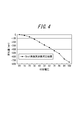
- FIG. 4 is a graph of Table 1, showing the amount of change in oscillation frequency based on the transmission frequency when the DC bias is 0V.
- the horizontal axis indicates the applied voltage (V), and the vertical axis indicates the amount of change (ppm). It has been experimentally confirmed that as the DC bias is increased, the coil inductance value moves in the direction of increasing, and the oscillation frequency is lowered.
- Table 2 shows the inductance value L of the coil calculated from the transmission frequency of the measurement result and the amount of change in the inductance value.
- the inductance value changes although the change amount and the number of digits of the capacitance are different.
- the amount of change in the inductance value is small.
- the coil is wound around the capacitor. This is because it is affected only indirectly.
- a coil may be formed by the internal electrode of the capacitor, and the coil may be built in the capacitor.
- FIG. 5 is a diagram illustrating an example of a configuration of a variable inductor in which a coil is built in a capacitor.
- the multilayer ceramic capacitor 22 includes a coil 21 inside the capacitor.
- a direct voltage (DC bias) is applied to the electrode 23 of the multilayer ceramic capacitor 22.
- FIG. 6 is a diagram showing another example of a configuration of a variable inductor in which a coil is built in a capacitor.
- a plurality of coils 31 are formed in a multilayer pattern inside the multilayer ceramic capacitor 32.
- a direct current voltage (DC bias) is applied to the electrode 33 of the multilayer ceramic capacitor 32.
- a variable inductor having a large inductance value can be formed by connecting the coils 31 in series. Further, a variable inductor having a large current capacity can be formed by connecting the coils 31 in parallel.
- a multilayer ceramic capacitor is used.
- the present invention is not limited to a multilayer ceramic capacitor, and any capacitor can be used as long as the dielectric constant and permeability change depending on the applied voltage. May be.
Landscapes
- Engineering & Computer Science (AREA)
- Power Engineering (AREA)
- Manufacturing & Machinery (AREA)
- Microelectronics & Electronic Packaging (AREA)
- Fixed Capacitors And Capacitor Manufacturing Machines (AREA)
- Coils Or Transformers For Communication (AREA)
Abstract
コイル11は、コイルの内部に、積層セラミックコンデンサ12を備えている。積層セラミックコンデンサ12の電極13には、直流電圧(DCバイアス)が印加される。積層セラミックコンデンサ12は、直流電圧(DCバイアス)が印加されると、誘電率εと透磁率μが変化し、静電容量が変化する。透磁率μが変化することによりコイル11のインダクタンス値も変化する。
Description
本願は、日本国特許出願第2011-066158号(2011年3月24日出願)の優先権の利益を主張し、これらの全内容を参照により本願明細書に取り込むものとする。
本発明は、インダクタンス特性を任意に調整できる可変インダクタに関する。
従来の可変インダクタは、コイルの中に挿入する磁性体コアを出し入れしてインダクタンス特性を任意に可変していた。従来の可変インダクタは、機械的駆動によりコイルの中に磁性体コアを出し入れするために、小型化には不向きである。したがって、現在でも、基本的に可変インダクタは利用されていない。
なお、従来技術として、無線機の送信部とアンテナとの間のインピーダンス整合をとる整合回路素子として用いられる可変インダクタが知られている(例えば、特許文献1参照)。
なお、従来技術として、無線機の送信部とアンテナとの間のインピーダンス整合をとる整合回路素子として用いられる可変インダクタが知られている(例えば、特許文献1参照)。
上述したように、現在でも、基本的には機械的駆動による可変インダクタは利用されていない。そのため、無線機における周波数チューニングでは、固定インダクタと可変コンデンサが用いられているが、固定インダクタと可変コンデンサにより周波数チューニングを行う方法では、小型化には限界があるため、機械的駆動のない小型化が可能な可変インダクタが必要とされている。
本発明は、このような問題点に鑑みてなされたものであり、本発明の目的は、機械的駆動によることなくインダクタンス値を任意に可変できる可変インダクタを提供することにある。
上記目的を達成するため、本発明の第1の態様に係る可変インダクタは、コイル内部に、誘電率および透磁率が変化するコンデンサを備えることを特徴とする。
第1の態様に係る可変インダクタにおいて、前記コンデンサに電圧を印加することにより前記誘電率および透磁率が変化することが好ましい。
第1の態様に係る可変インダクタにおいて、前記コンデンサは、積層セラミックコンデンサであることが好ましい。また、前記積層セラミックコンデンサには、F特性品に相当する誘電体が用いられることが好ましい。
また、本発明の第2の態様に係る可変インダクタは、誘電率および透磁率が変化するコンデンサの内部にコイルを備えることを特徴とする。
第2の態様に係る可変インダクタにおいて、前記コイルを複数有し、前記コイルそれぞれは、直列接続されていることが好ましい。
第2の態様に係る可変インダクタにおいて、前記コイルを複数有し、前記コイルそれぞれは、並列接続されていることが好ましい。
本発明は、積層セラミックコンデンサに印加する電圧を可変することにより、コイル内部の誘電率、透磁率が変化するので、機械的駆動によることなくインダクタンス値を任意に変化させることができる。
本発明の可変インダクタの実施の形態について説明する前に、積層セラミックコンデンサの特性について説明する。図1は、積層セラミックコンデンサの静電容量の変化特性を示す図である。縦軸は静電容量変化率(%)を示しており、横軸は直流電圧(V)を示している。誘電体材料にチタン酸バリウム(BaTiO3)を使う高誘電率系の積層セラミックコンデンサは、図1に示すように、積層セラミックコンデンサに直流電圧(DCバイアス)を印加すると、高容量コンデンサでは、静電容量がそのバイアスと共に変化する性質を有している。例えば、定格電圧が10Vで静電容量が10μFの積層セラミックコンデンサに直流4Vを印加すると、B特性品の場合は静電容量が約20%減少し、F特性品の場合は静電容量が約80%減少する。図1からF特性品が特に静電容量の減少が大きいことが分かる。
積層セラミックコンデンサの静電容量が印加電圧によって変化するのは、バイアス電圧の印加により見かけ上の誘電率εが変化するからである。
静電容量Cは、
C=εS/D
ε:誘電率
S:電極面積
D:電極間距離
で表される。積層セラミックコンデンサに、直流電圧(DCバイアス)を印加することにより、静電容量Cが変化するということは、電極面積Sおよび電極間距離Dは一定であるから、積層セラミックコンデンサ12の見かけ上の誘電率εが変化しているということである。
静電容量Cは、
C=εS/D
ε:誘電率
S:電極面積
D:電極間距離
で表される。積層セラミックコンデンサに、直流電圧(DCバイアス)を印加することにより、静電容量Cが変化するということは、電極面積Sおよび電極間距離Dは一定であるから、積層セラミックコンデンサ12の見かけ上の誘電率εが変化しているということである。
図2は、本発明の実施の形態に係る可変インダクタの構成を示す図である。コイル11は、コイルの内部に、積層セラミックコンデンサ12を備えている。積層セラミックコンデンサ12の電極13には、直流電圧(DCバイアス)が印加される。可変幅を大きくする場合には、積層セラミックコンデンサ12には、静電容量の変動の大きいF特性品に相当する誘電体を用いることが好ましい。
積層セラミックコンデンサ12の電極13に、直流電圧(DCバイアス)が印加され、積層セラミックコンデンサ12の見かけ上の誘電率εが変化すると、誘電率εと透磁率μとの間には、
εμ=1/v2
v:媒質中の光速
の関係があるので、それに伴い見かけ上の透磁率μも変化することになる。したがって、コイル11の内部の積層セラミックコンデンサ12の透磁率μが変化することになり、インダクタンスLは、
L=μSN2/d
S:コイルの断面積
N:コイルの巻数
d:コイルの長さ
で表されるので、透磁率μが変化することによりインダクタンスLも変化することになる。
εμ=1/v2
v:媒質中の光速
の関係があるので、それに伴い見かけ上の透磁率μも変化することになる。したがって、コイル11の内部の積層セラミックコンデンサ12の透磁率μが変化することになり、インダクタンスLは、
L=μSN2/d
S:コイルの断面積
N:コイルの巻数
d:コイルの長さ
で表されるので、透磁率μが変化することによりインダクタンスLも変化することになる。
上述のように、積層セラミックコンデンサ12に印加する直流電圧(DCバイアス)を可変することにより、コイル内部の誘電率、透磁率が変化するので、図2で示した可変インダクタは、機械的駆動によることなくインダクタンス値を任意に変化させることができる。
図3は、積層セラミックコンデンサの電極に印加する直流電圧(DCバイアス)を変化させたときに、積層セラミックコンデンサを内部に備えたコイルのインダクタンス値が、実際に変化することを確認するために用いたコルピッツ型の発振回路を示す図である。図3の回路にて、積層セラミックコンデンサの電極に印加するDCバイアスを1Vずつ増加させたときの、Vout における発振周波数を測定した。表1は、発振周波数の測定結果と発振周波数の変化量を示している。

図4は、表1をグラフ化させたもので、DCバイアスが0Vのときの発信周波数を基準にした発振周波数の変化量を示す図である。横軸が印加電圧(V)を示し、縦軸が変化量(ppm)を示す。DCバイアスを大きくしていくと、コイルのインダクタンス値が大きくなる方向に動き、発振周波数が下がっていることが実験的に確かめられた。
表2は、測定結果の発信周波数から算出したコイルのインダクタンス値Lとインダクタンス値の変化量を示している。
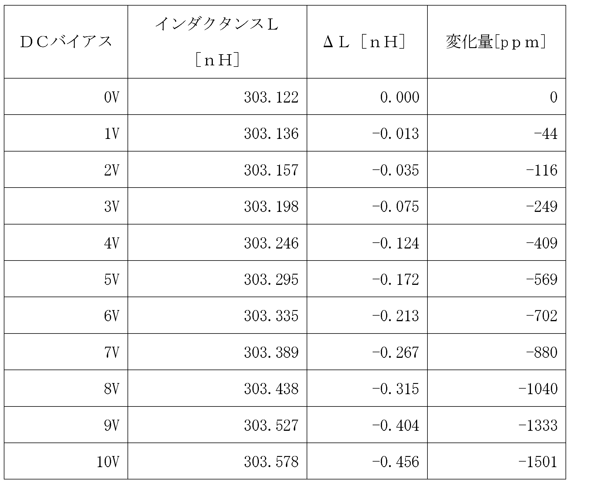
図1に示す積層セラミックコンデンサの静電容量の変化特性と比較すると、静電容量の変化量と桁数が違うが、インダクタンス値が、変化していることが分かる。インダクタンス値の変化量が小さいのは、積層セラミックコンデンサは、印加電圧による電極間誘電率の変化により、容量値が変化しても、コイルは、コンデンサの周囲に巻き回しているため、誘電率変化の影響を間接的にしか受けないためである。
また、DCバイアスを変化させたときに発振周波数の特性のみが変化し、他の特性に影響を与えていないことも確認できた。これにより、積層セラミックコンデンサへ印加するDCバイアスを可変とすることにより、コイルのインダクタンス値のみを可変できることが確認できた。
また、本発明は、コンデンサの内部電極でコイルを形成して、コイルをコンデンサに内蔵するようにしてもよい。図5は、コイルがコンデンサに内蔵された可変インダクタの構成の一例を示す図である。積層セラミックコンデンサ22は、コンデンサの内部に、コイル21を備えている。積層セラミックコンデンサ22の電極23には、直流電圧(DCバイアス)が印加される。
図6は、コイルがコンデンサに内蔵された可変インダクタの構成の他の例を示す図である。積層セラミックコンデンサ32の内部に、多層パターンで複数個のコイル31が形成されている。積層セラミックコンデンサ32の電極33には、直流電圧(DCバイアス)が印加される。コイル31を直列接続することで、大きなインダクタンス値の可変インダクタを形成することができる。また、コイル31を並列接続することで、電流容量の大きな可変インダクタを形成することができる。
なお、上述した実施形態では、積層セラミックコンデンサを用いているが、本発明は、積層セラミックコンデンサに限らず、印加電圧によって誘電率、透磁率が変化するものであれば、どのようなコンデンサを用いてもよい。
11、21、31 コイル
12、22、32 積層セラミックコンデンサ
13、32、33 電極
12、22、32 積層セラミックコンデンサ
13、32、33 電極
Claims (7)
- コイル内部に、誘電率および透磁率が変化するコンデンサを備えることを特徴とする可変インダクタ。
- 前記コンデンサに電圧を印加することにより前記誘電率および透磁率が変化することを特徴とする請求項1に記載の可変インダクタ。
- 前記コンデンサは、積層セラミックコンデンサであることを特徴とする請求項1に記載の可変インダクタ。
- 前記積層セラミックコンデンサには、F特性品に相当する誘電体が用いられていることを特徴とする請求項3に記載の可変インダクタ。
- 誘電率および透磁率が変化するコンデンサの内部にコイルを備えることを特徴とする可変インダクタ。
- 前記コイルを複数有し、
前記コイルそれぞれは、直列接続されていることを特徴とする請求項5に記載の可変インダクタ。 - 前記コイルを複数有し、
前記コイルそれぞれは、並列接続されていることを特徴とする請求項5に記載の可変インダクタ。
Applications Claiming Priority (2)
| Application Number | Priority Date | Filing Date | Title |
|---|---|---|---|
| JP2011066158A JP2012204491A (ja) | 2011-03-24 | 2011-03-24 | 可変インダクタ |
| JP2011-066158 | 2011-03-24 |
Publications (1)
| Publication Number | Publication Date |
|---|---|
| WO2012127875A1 true WO2012127875A1 (ja) | 2012-09-27 |
Family
ID=46879046
Family Applications (1)
| Application Number | Title | Priority Date | Filing Date |
|---|---|---|---|
| PCT/JP2012/002032 Ceased WO2012127875A1 (ja) | 2011-03-24 | 2012-03-23 | 可変インダクタ |
Country Status (2)
| Country | Link |
|---|---|
| JP (1) | JP2012204491A (ja) |
| WO (1) | WO2012127875A1 (ja) |
Cited By (2)
| Publication number | Priority date | Publication date | Assignee | Title |
|---|---|---|---|---|
| WO2014061672A1 (ja) * | 2012-10-18 | 2014-04-24 | 株式会社村田製作所 | コイル部品 |
| CN109786080A (zh) * | 2019-03-11 | 2019-05-21 | 中国计量大学 | 一种光控集成片上电感 |
Families Citing this family (1)
| Publication number | Priority date | Publication date | Assignee | Title |
|---|---|---|---|---|
| KR102325001B1 (ko) * | 2020-10-05 | 2021-11-10 | 김하정 | 투자율 조절장치를 갖는 자기 코어 및 자기 장치 |
Citations (3)
| Publication number | Priority date | Publication date | Assignee | Title |
|---|---|---|---|---|
| JPS61150204A (ja) * | 1984-12-24 | 1986-07-08 | Nec Corp | 電流制御型可変インダクタ |
| JPS62154706A (ja) * | 1985-12-27 | 1987-07-09 | Hitachi Ltd | インダクタ |
| JPH0260220U (ja) * | 1988-10-25 | 1990-05-02 |
-
2011
- 2011-03-24 JP JP2011066158A patent/JP2012204491A/ja active Pending
-
2012
- 2012-03-23 WO PCT/JP2012/002032 patent/WO2012127875A1/ja not_active Ceased
Patent Citations (3)
| Publication number | Priority date | Publication date | Assignee | Title |
|---|---|---|---|---|
| JPS61150204A (ja) * | 1984-12-24 | 1986-07-08 | Nec Corp | 電流制御型可変インダクタ |
| JPS62154706A (ja) * | 1985-12-27 | 1987-07-09 | Hitachi Ltd | インダクタ |
| JPH0260220U (ja) * | 1988-10-25 | 1990-05-02 |
Cited By (2)
| Publication number | Priority date | Publication date | Assignee | Title |
|---|---|---|---|---|
| WO2014061672A1 (ja) * | 2012-10-18 | 2014-04-24 | 株式会社村田製作所 | コイル部品 |
| CN109786080A (zh) * | 2019-03-11 | 2019-05-21 | 中国计量大学 | 一种光控集成片上电感 |
Also Published As
| Publication number | Publication date |
|---|---|
| JP2012204491A (ja) | 2012-10-22 |
Similar Documents
| Publication | Publication Date | Title |
|---|---|---|
| KR101386948B1 (ko) | 적층 콘덴서 및 전자기기 | |
| US9385682B2 (en) | High frequency component and filter component | |
| US9473103B2 (en) | High frequency component | |
| US8884720B2 (en) | Capacitance element and resonance circuit | |
| US10658720B2 (en) | Multilayer electronic component | |
| US9306529B2 (en) | Resonator and band pass filter | |
| US9525396B2 (en) | Tunable resonator | |
| WO2017100230A1 (en) | Voltage tunable multilayer capacitor | |
| JP2012005105A (ja) | 積層型フィルタ | |
| CN111433870B (zh) | 高电容可调多层电容器和阵列 | |
| WO2012127875A1 (ja) | 可変インダクタ | |
| KR101196842B1 (ko) | 나선형 인덕터를 이용한 lc 회로의 제어 장치 | |
| KR101153656B1 (ko) | 적층형 인덕터 | |
| JP6729839B2 (ja) | コイル部品および、これを含むフィルタ回路 | |
| US10284164B2 (en) | Circuit substrate, filter circuit, and capacitance element | |
| JP7706507B2 (ja) | 電圧調整可能な積層キャパシタの制御システムおよび方法 | |
| WO2009096474A1 (ja) | Lc複合部品 | |
| CN105977587A (zh) | 一种微波可调腔体滤波器 | |
| US20220181085A1 (en) | Multilayer capacitor | |
| RU99248U1 (ru) | Полосковый резонатор на двойной подвешенной подложке | |
| JP2010123649A (ja) | 積層デバイス | |
| CN107465396B (zh) | 一种多层非平面式绕线谐振滤波器 | |
| CN207251568U (zh) | 一种多层非平面式绕线谐振滤波器 | |
| TWI730322B (zh) | 電容電感諧振腔裝置及其製造方法 | |
| JP4169760B2 (ja) | 高周波フィルタ |
Legal Events
| Date | Code | Title | Description |
|---|---|---|---|
| 121 | Ep: the epo has been informed by wipo that ep was designated in this application |
Ref document number: 12761371 Country of ref document: EP Kind code of ref document: A1 |
|
| NENP | Non-entry into the national phase |
Ref country code: DE |
|
| 122 | Ep: pct application non-entry in european phase |
Ref document number: 12761371 Country of ref document: EP Kind code of ref document: A1 |