WO2012127841A1 - Optical-electric-field enhancement device, and measurement device provided with same - Google Patents
Optical-electric-field enhancement device, and measurement device provided with same Download PDFInfo
- Publication number
- WO2012127841A1 WO2012127841A1 PCT/JP2012/001866 JP2012001866W WO2012127841A1 WO 2012127841 A1 WO2012127841 A1 WO 2012127841A1 JP 2012001866 W JP2012001866 W JP 2012001866W WO 2012127841 A1 WO2012127841 A1 WO 2012127841A1
- Authority
- WO
- WIPO (PCT)
- Prior art keywords
- convex structure
- fine concavo
- photoelectric field
- structure layer
- metal
- Prior art date
Links
Images


Classifications
-
- H—ELECTRICITY
- H01—ELECTRIC ELEMENTS
- H01S—DEVICES USING THE PROCESS OF LIGHT AMPLIFICATION BY STIMULATED EMISSION OF RADIATION [LASER] TO AMPLIFY OR GENERATE LIGHT; DEVICES USING STIMULATED EMISSION OF ELECTROMAGNETIC RADIATION IN WAVE RANGES OTHER THAN OPTICAL
- H01S3/00—Lasers, i.e. devices using stimulated emission of electromagnetic radiation in the infrared, visible or ultraviolet wave range
- H01S3/30—Lasers, i.e. devices using stimulated emission of electromagnetic radiation in the infrared, visible or ultraviolet wave range using scattering effects, e.g. stimulated Brillouin or Raman effects
-
- B—PERFORMING OPERATIONS; TRANSPORTING
- B82—NANOTECHNOLOGY
- B82Y—SPECIFIC USES OR APPLICATIONS OF NANOSTRUCTURES; MEASUREMENT OR ANALYSIS OF NANOSTRUCTURES; MANUFACTURE OR TREATMENT OF NANOSTRUCTURES
- B82Y20/00—Nanooptics, e.g. quantum optics or photonic crystals
-
- G—PHYSICS
- G01—MEASURING; TESTING
- G01N—INVESTIGATING OR ANALYSING MATERIALS BY DETERMINING THEIR CHEMICAL OR PHYSICAL PROPERTIES
- G01N21/00—Investigating or analysing materials by the use of optical means, i.e. using sub-millimetre waves, infrared, visible or ultraviolet light
- G01N21/17—Systems in which incident light is modified in accordance with the properties of the material investigated
- G01N21/55—Specular reflectivity
- G01N21/552—Attenuated total reflection
- G01N21/553—Attenuated total reflection and using surface plasmons
- G01N21/554—Attenuated total reflection and using surface plasmons detecting the surface plasmon resonance of nanostructured metals, e.g. localised surface plasmon resonance
-
- G—PHYSICS
- G01—MEASURING; TESTING
- G01N—INVESTIGATING OR ANALYSING MATERIALS BY DETERMINING THEIR CHEMICAL OR PHYSICAL PROPERTIES
- G01N21/00—Investigating or analysing materials by the use of optical means, i.e. using sub-millimetre waves, infrared, visible or ultraviolet light
- G01N21/62—Systems in which the material investigated is excited whereby it emits light or causes a change in wavelength of the incident light
- G01N21/63—Systems in which the material investigated is excited whereby it emits light or causes a change in wavelength of the incident light optically excited
- G01N21/64—Fluorescence; Phosphorescence
- G01N21/645—Specially adapted constructive features of fluorimeters
- G01N21/648—Specially adapted constructive features of fluorimeters using evanescent coupling or surface plasmon coupling for the excitation of fluorescence
-
- G—PHYSICS
- G01—MEASURING; TESTING
- G01N—INVESTIGATING OR ANALYSING MATERIALS BY DETERMINING THEIR CHEMICAL OR PHYSICAL PROPERTIES
- G01N21/00—Investigating or analysing materials by the use of optical means, i.e. using sub-millimetre waves, infrared, visible or ultraviolet light
- G01N21/62—Systems in which the material investigated is excited whereby it emits light or causes a change in wavelength of the incident light
- G01N21/63—Systems in which the material investigated is excited whereby it emits light or causes a change in wavelength of the incident light optically excited
- G01N21/65—Raman scattering
- G01N21/658—Raman scattering enhancement Raman, e.g. surface plasmons
Definitions
- the present invention relates to a photoelectric field enhancement device having a fine metal relief structure capable of inducing localized plasmons and a measurement apparatus having a photoelectric field enhancement device.
- Raman spectroscopy is a method of obtaining a spectrum of Raman scattered light (Raman spectrum) by dispersing scattered light obtained by irradiating a substance with single wavelength light, and is used for identification of substances.
- Raman spectroscopy in order to enhance weak Raman scattered light, there is Raman spectroscopy using surface enhanced Raman (SERS: Surface Enhanced Raman Scattering), a photoelectric field enhanced by localized plasmon resonance ( Non-patent document 1).
- SERS Surface Enhanced Raman Scattering
- a photoelectric field enhanced by localized plasmon resonance a photoelectric field enhanced by localized plasmon resonance
- Surface-enhanced Raman spectroscopy can be carried out by using a substrate having a metal concavo-convex structure on the surface as a carrier (substrate) for supporting an object.
- a substrate having a metal fine concavo-convex structure on its surface As a substrate having a metal fine concavo-convex structure on its surface, a substrate in which concavo-convex is provided on the surface of a Si substrate and a metal film is formed on the concavo-convex surface is mainly used (see Patent Documents 1 to 3).
- the surface of the Al substrate is anodized to form a part of the metal oxide layer (Al 2 O 3 ), which is naturally formed inside the metal oxide layer during the anodic oxidation process, and is opened on the surface of the metal oxide layer.
- a substrate in which a plurality of fine holes are filled with metal has also been proposed (see Patent Document 4).
- Patent Documents 1 to 4 and the like have a fine concavo-convex structure formed on an opaque substrate surface such as Si or Al, and a metal film is formed on the surface of the fine concavo-convex structure, or It is the structure which embedded the metal in the recessed part.
- Patent Document 4 gives an example using a transparent substrate such as a glass substrate, but the fine concavo-convex structure itself is made of an opaque material such as silicon or germanium.
- the conventional Raman spectrometer is configured to detect Raman scattered light from the sample surface side.
- the sample when a sample of ⁇ m order or more such as a cell is used as a subject, the sample itself becomes a shield against Raman scattered light, and it is difficult to receive weak Raman light with high S / N.
- the present invention has been made in view of the above circumstances, and an object thereof is to provide a photoelectric field enhancement device capable of detecting Raman scattered light with higher sensitivity and a measurement apparatus including the device.
- the photoelectric field enhancement device of the present invention comprises a transparent substrate having a fine concavo-convex structure on the surface, and a metal fine concavo-convex structure layer formed on the surface of the fine concavo-convex structure,
- the metal fine concavo-convex structure layer has a fine concavo-convex structure in which an interval between adjacent convex portions is smaller than an interval between adjacent convex portions of the fine concavo-convex structure of the transparent substrate corresponding to the adjacent convex portions,
- the light irradiated on the metal fine concavo-convex structure layer generates an enhanced photoelectric field on the surface by the photoelectric field enhancement effect of localized plasmons induced on the surface of the metal fine concavo-convex structure layer. It is characterized by.
- the metal fine uneven structure layer has the same uneven structure as the fine uneven structure of the transparent substrate. Since the interval between the portions is equivalent to the interval between the adjacent convex portions of the fine concavo-convex structure of the substrate corresponding to the adjacent convex portions, the present invention has a uniform metal film on the fine concavo-convex structure of the transparent substrate. What is formed is not included.
- interval between adjacent convex parts is in the half depth of the depth from the vertex of the lower convex part between the convex parts adjacent in cross section to the deepest part of the recessed part between the adjacent convex parts. It is defined by the distance between the adjacent convex portions.
- the cross section can be observed with a scanning electron microscope (SEM) or the like, and the interval between the convex portions can be obtained from the SEM image.
- the metal fine concavo-convex structure layer may partially include a portion where the interval between adjacent convex portions is the same as or larger than the interval between adjacent convex portions of the corresponding fine concavo-convex structure of the substrate.
- the metal fine uneven structure layer has a fine uneven structure capable of generating localized plasmons.
- a fine concavo-convex structure capable of generating localized plasmons generally means that the average size of at least one of the length in the direction perpendicular to the substrate and the length in the horizontal direction of the concavo-convex structure is the excitation light.
- the concavo-convex structure is smaller than the wavelength.
- the fine concavo-convex structure of the metal fine concavo-convex structure layer is on the surface opposite to the transparent substrate of the metal fine concavo-convex structure layer with respect to light irradiated from the transparent substrate side. It is preferable that the photoelectric field is enhanced efficiently.
- the thickness is preferably 400 nm or less for gold and 90 nm or less for silver.
- the thickness in the case of this vapor deposition film formation means having vapor-deposited with the vapor deposition amount which is 400 nm or less or 90 nm or less when a metal (gold
- the fine concavo-convex structure of the metal fine concavo-convex structure layer preferably includes a portion where the distance between adjacent convex portions is 20 nm or less.
- Image processing can be binarized and obtained by statistical processing.
- the term “transparent” means that the transmittance is 50% or more with respect to irradiated light and light generated from a subject by the light. Note that the transmittance of these lights is preferably 75% or more, and more preferably 90% or more.
- the fine concavo-convex structure of the metal fine concavo-convex structure layer is a granular fine structure formed by agglomerating the metal constituting the metal fine concavo-convex structure layer on the surface of the fine concavo-convex structure of the transparent substrate. It is preferable that it consists of.
- metal agglomerates means that when a metal fine concavo-convex structure layer is formed on the fine concavo-convex structure of the substrate, the metal concentrates on the convex portions to form lumps. Is called granular.
- the aspect ratio of the convex part is 0.5 or more (length in the direction perpendicular to the substrate / length in the horizontal direction to the substrate), that is, metal fine
- it is desirable that the length of the convex portion in the direction perpendicular to the substrate is larger than the length in the direction horizontal to the substrate.
- the metal fine concavo-convex structure layer only needs to be made of a metal that generates localized plasmon when irradiated with the light, but gold (Au), silver (Ag), copper (Cu), aluminum (Al), It is preferably made of platinum (Pt) or an alloy containing these as a main component. In particular, Au or Ag is preferable.
- the transparent substrate is a transparent fine concavo-convex structure made of a material different from the transparent substrate main body and the transparent concavo-convex structure provided on the surface of the transparent substrate main body. It can consist of layers.
- the transparent fine concavo-convex structure layer is made of at least one of a metal hydroxide and a metal oxide hydroxide, that is, a metal hydroxide, a metal oxide hydroxide, or both hydroxides thereof. It can form suitably.
- the transparent fine concavo-convex structure layer is composed of at least one of buyer light (Al [OH] 3 ) and boehmite (AlOOH).
- it may be made of a hydroxide of titanium (Ti) or a hydroxide of Ti oxide.
- the transparent substrate may be provided with a second fine concavo-convex structure functioning as an antireflection film on the back surface.
- the second fine concavo-convex structure may be composed of a second transparent fine concavo-convex structure layer made of a material different from that of the transparent substrate, and the second transparent fine concavo-convex structure layer may be It can be suitably formed from at least one of a metal hydroxide and a metal oxide hydroxide, that is, a metal hydroxide, a metal oxide hydroxide, or both hydroxides thereof.
- the second transparent fine concavo-convex structure layer is particularly preferably made of at least one of buyer light (Al [OH] 3 ) or boehmite (AlOOH).
- the photoelectric field enhancing device of the present invention can be a sample cell including a liquid sample holding member for holding a liquid sample on the metal fine concavo-convex structure layer of the transparent substrate.
- the liquid sample holding member may be a flow cell type sample cell having a liquid inflow portion and an outflow portion.
- the measuring apparatus of the present invention comprises the photoelectric field enhancing device of the present invention, An excitation light irradiation unit for irradiating the photoelectric field enhancement device with excitation light; And a light detection unit that detects light generated by the irradiation of the excitation light.
- the photoelectric field enhancement device of the present invention comprises a transparent substrate having a fine concavo-convex structure on the surface, and a metal fine concavo-convex structure layer formed on the surface of the fine concavo-convex structure, and the metal fine concavo-convex structure layer is an adjacent convex portion.
- the metal fine concavo-convex structure has a fine concavo-convex structure whose interval is smaller than the interval between adjacent concavo-convex parts of the fine concavo-convex structure of the transparent substrate corresponding to the adjacent convex parts. Localized plasmons can be effectively induced on the surface of the layer, and a photoelectric field enhancement effect by the localized plasmons can be generated.
- a hot spot can be generated in that region.
- the photoelectric field enhancing device of the present invention By placing the subject on the photoelectric field enhancing device of the present invention and irradiating the region where the subject is placed with light, the light generated from the subject is enhanced by the photoelectric field enhancing effect. It becomes possible to detect light with sensitivity.
- the photoelectric field enhancement device of the present invention uses a transparent substrate, it can irradiate light (excitation light) from either the front surface side of the metal fine concavo-convex structure layer or the back surface side of the transparent substrate, Light (detection light) generated from the subject by this light irradiation can also be detected from either the front surface side of the metal fine concavo-convex structure layer or the back surface side of the transparent substrate. Depending on the type, size, etc. of the specimen, excitation light irradiation and detection light detection can be performed from either the front surface side of the metal fine concavo-convex structure layer or the back surface side of the transparent substrate. You can choose to do it freely. That is, if the photoelectric field enhancement device of the present invention is used, the degree of freedom in measurement is high, and detection can be performed with a higher S / N.
- the fine uneven structure on the surface of the transparent substrate is formed as a transparent fine uneven structure layer from a metal hydroxide or a metal oxide hydroxide
- a transparent fine concavo-convex structure can be produced by a very simple manufacturing method in which high temperature water is reacted. Therefore, the manufacturing cost can be remarkably suppressed as compared with the conventional device.
- substrate SEM image of boehmite layer surface
- Enlarged view of part IVB at the bottom of the side surface of the photoelectric field enhancement substrate 2 shown in FIG. 4A Diagram showing the wavelength dependence of the light reflectivity of the boehmite layer Plan view showing a photoelectric field enhancement sample cell 3 according to a third embodiment of the photoelectric field enhancement device.
- FIG. 6A Schematic diagram showing the configuration of an enhanced Raman spectroscopic device provided with a photoelectric field enhancing substrate 1 Schematic showing an example of design change of an enhanced Raman spectrometer Schematic diagram showing the configuration of an enhanced Raman spectrometer equipped with a photoelectric field enhancing sample cell 3 Graph showing the Raman spectrum distribution obtained for the measurement sample Graph showing the dependence of Raman signal intensity obtained on measurement sample on Au vapor deposition film thickness
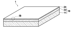
- FIG. 1A is a perspective view showing a photoelectric field enhancement substrate 1 according to the first embodiment of the photoelectric field enhancement device of the present invention
- FIG. 1B is a part of a side surface of the photoelectric field enhancement substrate 1 shown in FIG. 1A. It is an enlarged view of IB.
- the photoelectric field enhancing substrate 1 includes a transparent substrate 10 having a fine uneven structure 23 on the surface, and a metal fine uneven structure layer 24 formed on the surface of the fine uneven structure 23.
- excitation light irradiated to the fine concavo-convex structure 25 of the metal fine concavo-convex structure layer 24, and the metal fine concavo-convex structure layer 24 is induced by this local plasmon resonance. This produces an enhanced photoelectric field on the surface of the film.
- the metal fine concavo-convex structure layer 24 has a fine concavo-convex structure in which the interval between adjacent convex portions is smaller than the interval between adjacent convex portions of the fine concavo-convex structure 23 of the transparent substrate 10 that corresponds between the adjacent convex portions.
- the interval Wm between the convex portion 25a and the convex portion 25b adjacent thereto corresponds to the convex portions 25a and 25b. It suffices if there is a portion that is smaller than the interval Wb between the convex portion 23a and the convex portion 23b of the fine concavo-convex structure 23 of the transparent substrate.
- the interval Wm is half the depth Dm from the apex of the lower convex portion 25b of the adjacent convex portions 25a and 25b to the deepest portion 25c of the concave portion between both convex portions 25a and 25b.
- the interval Wb is half the depth Db from the apex of the lower convex portion 23b of the adjacent convex portions 23a and 23b to the deepest portion 23c of the concave portion between both convex portions 23a and 23b. This is the distance between the convex portions 23a and 23b at the position of the depth Db / 2.
- the convex portions 24a are rounded and the distance between adjacent convex portions is smaller than when the metal is simply formed in a film shape along the fine concavo-convex structure 23 of the transparent substrate 10.
- the fine concavo-convex structure 25 of the metal fine concavo-convex structure layer 24 is such that at least one of the length in the direction perpendicular to the substrate and the length in the direction horizontal to the substrate is shorter than the wavelength of the excitation light. Any fine concavo-convex structure may be used as long as it can generate localized plasmons on the surface of the metal fine concavo-convex structure layer 24.
- the convex portions of the metal fine concavo-convex structure layer 24 are preferably in the form of particles formed by aggregation of metals. It is desirable that the granular convex portions have an aspect ratio (length in the direction perpendicular to the substrate / length in the horizontal direction on the substrate) of 0.5 or more.
- the average depth from the top of the convex portion of the fine concave-convex structure 25 of the metal fine concave-convex structure layer 24 to the bottom of the adjacent concave portion is 200 nm or less, and the average pitch between the vertices of the nearest convex portions separating the concave portions is 200 nm or less. Preferably there is.
- the average thickness of the metal fine concavo-convex structure layer 24 generates an efficiently enhanced photoelectric field on the surface opposite to the transparent substrate of the metal fine concavo-convex structure layer with respect to light irradiated from the transparent substrate side. Thickness is preferred.
- the thickness is preferably 400 nm or less for gold and 90 nm or less for silver. The thickness at this time is not a measured value of the thickness, but means that the thickness is deposited on the flat plate substrate by the deposition amount required for depositing a metal such as gold or silver.
- the distance between all adjacent convex portions of the fine concavo-convex structure in the metal fine concavo-convex structure layer is smaller than the interval between adjacent convex portions of the corresponding fine concavo-convex structure of the substrate.
- the effect of enhancing the photoelectric field becomes more prominent as the number of adjacent convex portions of the metal fine concavo-convex structure layer that is smaller than the interval between adjacent convex portions of the corresponding fine concavo-convex structure of the substrate increases.
- a very strong photoelectric field enhancement field called a hot spot is generated in the gap between the convex portions by light irradiation. For this reason, it is preferable that there are many places where the distance between adjacent convex portions is 20 nm or less. In addition, adjacent convex parts may be contacting partially.
- the metal fine concavo-convex structure layer 24 is particularly preferably a granular convex part formed so that the convex part extends in a granular manner from the surface of the fine concavo-convex structure 23 of the transparent substrate 10. If it is granular, the surface area increases, so the number of analytes attached to the metal surface can be increased, leading to an increase in detection light.
- the metal constituting the metal fine concavo-convex structure layer 24 may be any metal that can generate localized plasmon when irradiated with excitation light.
- Au or Ag is preferable.
- the transparent substrate 10 includes a transparent substrate body 11 made of glass or the like, and a transparent fine substrate made of a material different from the transparent substrate body 11 constituting the fine uneven structure 23 provided on the surface of the transparent substrate 10.
- the concavo-convex structure layer 22 is used.
- the transparent fine concavo-convex structure layer 22 is preferably a boehmite layer, but the transparent fine concavo-convex structure layer 22 may be made of Bayerlite in addition to boehmite. Moreover, you may be comprised from the hydroxide of another metal or the hydroxide of a metal oxide.
- the fine concavo-convex structure 23 is not limited to the one made of a material different from that of the transparent substrate body, but may be made of the same material as the substrate body by processing the surface of the transparent substrate body.
- a glass substrate having a surface with a fine concavo-convex structure formed by dry etching treatment with any of lithography, ion beam lithography, and nanoimprint may be used as the transparent substrate.
- the fine concavo-convex structure 23 is constituted by the boehmite layer 22.
- the transparent fine concavo-convex structure 23 made of a metal such as a boehmite layer or a hydroxide of a metal oxide has various sizes (vertical angle sizes) and orientations, but has a generally serrated cross section. have.
- the transparent fine concavo-convex structure 23 may be any structure as long as the metal fine concavo-convex structure layer 24 can be formed on the transparent fine concavo-convex structure 23.
- the pitch is the distance between the vertices of the nearest adjacent convex portions across the concave portion
- the depth is the distance from the convex vertex to the bottom of the adjacent concave portion.
- a plate-like transparent substrate body 11 is prepared, and the transparent substrate body 11 is washed with acetone and methanol. Thereafter, the aluminum 20 is deposited on the surface of the substrate body 11 by a sputtering method to a thickness of about several tens of nanometers. Thereafter, the transparent substrate body 11 with aluminum 20 is immersed in boiling pure water, and is taken out after several minutes (about 5 minutes). By this boiling treatment (boehmite treatment), the aluminum 20 becomes transparent and becomes a boehmite layer 22 constituting a fine concavo-convex structure. Next, by depositing a metal on the boehmite layer 22, a metal fine concavo-convex structure layer 24 is generated on the boehmite layer 22.
- the photoelectric field enhancing substrate 1 can be manufactured by the above processing.
- FIG. 3A shows a boehmite of a transparent substrate comprising a boehmite layer formed by sputtering a 25 nm aluminum film on a transparent substrate body (BK-7; Corning Eagle 2000) and then boiling it for 5 minutes.
- FIG. 3B to FIG. 3D are SEM images obtained by photographing the surface of the substrate and the substrate surface on which Au was deposited on the boehmite layer by 30 nm, 60 nm, and 150 nm, respectively, with SEM (Hitachi S4100).
- Al is vapor-deposited for 30 nm, 60 nm, and 150 nm” means that it is vapor-deposited with a vapor deposition amount of 30 nm, 60 nm, and 150 nm when vapor-deposited on a flat substrate.
- FIGS. 3A to 3D white portions are observed as convex portions, and gray portions are observed as concave portions.
- the uneven pattern is irregular, it is uniformly formed on the entire surface, and the in-plane uniformity of the fine uneven structure is high.
- the concavo-convex structure is composed of a number of ridge-shaped convex portions.
- the uneven structure cross section of the boehmite layer has a sawtooth shape as schematically shown in FIG. 1B. As shown in FIG.
- the convex portions of the concavo-convex structure formed in the boehmite layer are thick and the convex portion interval is narrow.
- the concave fine concavo-convex structure of the metal fine concavo-convex structure layer shown in FIG. 3B is a concavo-convex structure having a convex portion in which the ridge-like convex structure seen on the surface of the boehmite layer is substantially maintained.
- the convex portions are observed in a granular form, and the interval between the convex portions becomes closer. It is observed as an uneven structure different from the uneven structure on the boehmite layer surface.
- FIG. 3E is an SEM image of a cross section of a metal fine concavo-convex structure layer obtained by depositing 150 nm of Au on the boehmite layer. From the image of this cross section, the convex portion extends upward from the boehmite side and has a larger aspect ratio, and the metal fine concavo-convex structure is a granular fine structure in which a large number of granular convex portions are formed. I understand that. In addition, a large number of regions in which the intervals between the granular convex portions are very close are formed.
- FIG. 4A is a perspective view showing the photoelectric field enhancement substrate 2 of the present embodiment
- FIG. 4B is an enlarged view of a part IVB at the lower side of the photoelectric field enhancement substrate 2 shown in FIG. 4A.
- the photoelectric field enhancement substrate 2 of the present embodiment includes a second transparent fine concavo-convex structure layer 28 on the back side of the photoelectric field enhancement substrate 1 of the first embodiment.
- the second transparent fine concavo-convex structure layer 28 is the same as the first fine concavo-convex structure layer 22 provided on the surface side of the transparent substrate 10, and can be composed of a boehmite layer.
- the fine uneven structure layer 28 on the back side functions as an antireflection film when irradiated with light.
- the photoelectric field enhancement substrate 2 of the present embodiment is formed by depositing aluminum not only on the front surface but also on the back surface of the transparent substrate body 11 in the method for producing the photoelectric field enhancement substrate 1 of the first embodiment, and then boiled. Can be obtained. By boiling in pure water, the front and back aluminum becomes boehmite, and the same transparent fine uneven structure layers 22 and 28 can be provided on the front and back surfaces.
- FIG. 5 shows a boehmite layer formed on a substrate having a boehmite layer formed by sputtering for 5 minutes after sputtering 50 nm aluminum on a transparent substrate (BK-7; Corning Eagle 2000). It shows the reflectance when light is incident from the surface side from the direction perpendicular to the surface. In the case of this example, a reflectance of about 0.1% is achieved for a wavelength near 650 nm. The wavelength with the lowest reflectivity can be adjusted by controlling the interference by changing the thickness of the aluminum that is first sputtered.
- FIG. 6A is a plan view showing the photoelectric field enhancing sample cell 3 of the third embodiment
- FIG. 6B is a sectional view taken along the line VIB-VIB of the photoelectric field enhancing sample cell 3 shown in FIG. 6A.
- the photoelectric field enhancing sample cell 3 of this embodiment includes a transparent substrate main body 31, a transparent fine uneven structure layer 32 provided on the surface thereof, and a metal fine uneven structure layer 34 provided on the fine uneven structure layer 32. And a liquid sample holding member 35 for holding a liquid sample on the metal fine concavo-convex structure layer 34.
- the photoelectric field enhancement substrate 30 has substantially the same configuration as the photoelectric field enhancement substrate 1 of the first embodiment. That is, the transparent fine uneven structure layer 32 and the metal fine uneven structure layer 34 are the same as the transparent fine uneven structure layer 22 and the metal fine uneven structure layer 24 of the first photoelectric field enhancement device 1 shown in FIG. 1B. The constituent materials and the forming method are also the same.
- the liquid sample holding member 35 holds, for example, a liquid sample on the metal fine concavo-convex structure layer 34 and forms a liquid sample flow path 36a, an inlet (inlet) 38a for injecting the sample, and a flow
- a transparent upper plate 38 such as a glass plate provided with a discharge port (outlet) 38b for discharging the liquid sample flowing down the path 36a can be used.
- the photoelectric field enhancing sample cell 3 of the present embodiment can be obtained by fabricating the photoelectric field enhancing substrate 30 by the same method as that of the substrate 1 of the first embodiment and then bonding the spacer portion 36 and the upper plate 38. it can.
- the spacer portion 36 and the upper plate 38 may be integrally formed.
- the spacer part 36 may be formed integrally with the transparent substrate body 31.
- the flow channel sample cell (flow cell) type photoelectric field enhancement device provided with an inlet and an outlet has been described. It is good also as a photoelectric field enhancement sample cell which hold
- a second transparent functioning as an antireflection film is provided on the back surface of the region where the metal fine concavo-convex structure layer 34 of the photoelectric field enhancement substrate 30 is provided, like the photoelectric field enhancement substrate 2 of the second embodiment. You may make it provide a fine fine uneven
- the photoelectric field enhancement device of the present invention described in each of the above embodiments has a subject placed on the metal fine concavo-convex structure layer of the device, irradiated with excitation light to the place where the subject is placed, and the excitation light. It can be suitably used for a measurement method and apparatus for detecting light generated from a subject by irradiation of. For example, it can be applied to enhanced Raman spectroscopy, fluorescence detection method, etc., can be used as a Raman enhancement device in enhanced Raman spectroscopy, and can be used as a fluorescence enhancement device in fluorescence detection method.
- the photoelectric field enhancement device of the present invention is used not only for detection of Raman scattered light and fluorescence, but also for detection of Rayleigh scattered light, Mie scattered light, second harmonics, and the like generated from an object irradiated with excitation light.
- enhanced light can be detected by the enhanced photoelectric field associated with localized plasmon resonance.
- FIG. 7 is a schematic diagram showing a configuration of an enhanced Raman spectroscopic device including the photoelectric field enhancing substrate 1 according to the first embodiment described above.
- the Raman spectroscopic device 100 includes the above-described photoelectric field enhancement substrate 1, the excitation light irradiation unit 140 that irradiates the photoelectric field enhancement substrate 1 with the excitation light L1, and the photoelectric field enhancement emitted from the subject S. And a light detection unit 150 for detecting Raman scattered light L2 enhanced by the action of the substrate.
- the excitation light irradiation unit 140 includes a semiconductor laser 141 that emits the excitation light L1, a mirror 142 that reflects the light L1 emitted from the semiconductor laser 141 toward the substrate 1, and the excitation light L1 reflected by the mirror 142. Transmitted through the half mirror 144 and the half mirror 144 that reflects light from the substrate 1 side including the enhanced Raman scattered light L2 generated from the subject S by irradiation of the excitation light L1 to the light detection unit 150 side And a lens 146 that condenses the excitation light L1 in a region of the photoelectric field enhancement substrate 1 on which the subject S is placed.
- the light detection unit 150 absorbs the excitation light L1 out of the light reflected by the half mirror 144 and transmits the other light, and a pin provided with a pinhole 152 for removing noise light.
- a lens 154 for condensing the enhanced Raman scattered light L2 emitted from the Hall plate 153, the subject S, and transmitted through the lens 146 and the notch filter 151 to the pinhole 152, and the Raman scattered light passing through the pinhole 152 Is provided with a lens 156 for collimating light and a spectroscope 158 for detecting enhanced Raman scattered light.
- Excitation light L1 is emitted from the semiconductor laser 141 of the light irradiation unit 140, the excitation light L1 is reflected to the substrate 1 side by the mirror 142, passes through the half mirror 144 and is collected by the lens 146, and the photoelectric field enhancement substrate 1 Irradiated on top.
- the irradiation of the excitation light L1 induces localized plasmon resonance in the metal fine concavo-convex structure layer 24 of the photoelectric field enhancing substrate 1, and an enhanced photoelectric field is generated on the surface of the metal fine concavo-convex structure layer 24.
- the Raman scattered light L2 emitted from the subject S enhanced by the enhanced photoelectric field passes through the lens 146 and is reflected by the half mirror 144 toward the spectroscope 158 side. At this time, the excitation light L1 reflected by the photoelectric field enhancement substrate 1 is also reflected by the half mirror 144 and reflected to the spectroscope 158 side, but the excitation light L1 is cut by the notch filter 151.
- the wavelength of Rayleigh scattered light (or Mie scattered light) is the same as that of the excitation light L 1, so that it is cut by the notch filter 151 and does not enter the spectroscope 158.
- the Raman scattered light L2 enters the spectroscope 158 and is subjected to Raman spectrum measurement.
- the Raman spectroscopic device 100 of the present embodiment is configured using the photoelectric field enhancement substrate 1 of the above embodiment, and since the Raman enhancement is effectively performed, the data reliability is high and the data reproducibility is high. Good high-precision Raman spectroscopic measurement can be performed. Since the in-plane uniformity of the surface concavo-convex structure of the photoelectric field enhancing substrate 1 is high, data with good reproducibility can be obtained even if the same sample is measured by changing the light irradiation location. Therefore, it is possible to obtain a plurality of data by changing the light irradiation location for the same sample, thereby improving the reliability of the data.
- the metal fine concavo-convex structure layer and the subject can be detected from the back side of the transparent substrate without being shielded by the subject itself.
- the present inventors confirmed that the enhanced Raman scattering light can be detected from the back side of the transparent substrate without being affected by the metal fine uneven structure layer if the metal fine uneven structure layer has a certain thickness. (See Examples below).
- the Raman spectroscopic apparatus 100 is configured so that excitation light is incident from the side opposite to the sample holding surface (front surface) of the photoelectric field enhancing device 1 (back surface of the device) and Raman scattered light is detected.
- the excitation light L1 is incident from the surface side (sample holding surface) of the metal fine concavo-convex structure layer 24 and the Raman scattering is performed as in the conventional device. You may comprise so that the light L2 may be detected.
- either the excitation light irradiation part or the light detection part may be arranged on the surface side of the metal fine concavo-convex structure layer 24 and the other may be arranged on the back side of the substrate 1.
- the photoelectric field enhancement device of the present invention uses a transparent substrate, light can be irradiated from either the surface side of the metal fine concavo-convex structure layer or the back side of the transparent substrate, Light generated from the sample by this light irradiation can also be detected from either the surface side of the metal fine concavo-convex structure layer or the back side of the transparent substrate. Therefore, depending on the type, size, etc. of the subject, irradiation of excitation light and detection of detection light can be performed from either the front surface side of the metal fine concavo-convex structure layer or the back surface side of the transparent substrate. The degree is high, and it becomes possible to detect at a higher S / N.
- FIG. 9 is a schematic diagram illustrating a schematic configuration of a Raman spectroscopic device 120 including a flow cell that is the photoelectric field enhancement device 3 of the above-described third embodiment.
- the Raman spectroscopic device 120 shown in FIG. 9 differs from the Raman spectroscopic device 100 shown in FIG. 7 in that a flow cell type photoelectric field enhancing sample cell 3 is provided instead of the photoelectric field enhancing substrate 1.
- a flow cell type photoelectric field enhancement device Raman spectroscopy can be measured while flowing a liquid sample as an object.
- the measurement of the flow cell type device 3 may be configured such that excitation light is incident from the surface side of the metal fine concavo-convex structure layer and Raman scattered light is detected from the surface side of the metal fine concavo-convex structure layer.
- the transmittance and the absorptance of the liquid sample with respect to the Raman scattered light may vary with the movement of the liquid sample. As shown in FIG. 4, it is preferable that the Raman scattered light is detected from the back side of the substrate 30.
- the photoelectric field enhancement device of the present invention can be applied to a plasmon enhanced fluorescence detection apparatus.
- the subject may be placed on the metal fine concavo-convex structure layer of the photoelectric field enhancing device, and excitation light may be irradiated from the subject side to detect the enhanced fluorescence from the subject side.
- the excitation light may be irradiated from the back side of the transparent substrate, and the fluorescence may be detected from the back side.
- you may irradiate excitation light from the subject side and you may comprise so that fluorescence may be detected from the transparent substrate back surface side.
- Method for producing photoelectric field enhancement substrate As the transparent substrate body 11, a glass substrate (BK-7; Eagle 2000 manufactured by Corning) was used. After ultrasonic cleaning (45 kHz) for 5 minutes with acetone and 5 minutes with methanol, 25 nm of aluminum 20 was laminated on the glass substrate 11 using a sputtering apparatus (manufactured by Canon Anelva). In addition, the aluminum thickness was measured using the surface shape measuring device (made by TENCOR), and it confirmed that thickness was 25 nm (+/- 10%).
- Raman scattered light was detected using a microscopic Raman spectroscope (HR800).
- HR800 Raman spectroscope
- laser light having a peak wavelength of 785 nm was used and observed at a magnification of 20 times.
- FIG. 10 is a graph showing a Raman shift spectrum distribution obtained by detecting Raman scattered light from the front and back of a substrate using a sample (Example 2) in which Au is deposited by 60 nm.
- the measurement from the surface of the substrate is a method in which excitation light is irradiated from the dye surface side on the metal fine concavo-convex structure layer, and Raman scattered light is detected from the dye surface side on the metal fine concavo-convex structure layer.
- the measurement from the back side is the one that irradiates excitation light from the transparent fine concavo-convex structure side under the metal fine concavo-convex structure layer (irradiates excitation light from the back side of the substrate) and detects Raman scattered light from the back side of the substrate. is there.
- FIG. 10 shows that the Raman shift signal can be detected with the same intensity at almost the same location on the front and back of the substrate.
- Raman measurement there was no example of detecting a Raman signal from the back side of the substrate, but according to the Raman measurement using the photoelectric field enhancement device of the present invention, the Raman signal was detected from the back side of the substrate. It is clear that it can be detected.
- the dye used as a specimen in the measurement sample was dried and fixed, and the thickness of the specimen was very thin. Therefore, the signal intensity from the front and back surfaces was the same level.
- Raman spectroscopy when performing Raman spectroscopy on a sample having a thickness of the order of 1 ⁇ m such as a cell, it is better to detect the signal near the interface between the metal fine concavo-convex structure layer and the sample with a high enhancement effect from the back side. It is considered advantageous.
- FIG. 11 shows the peak intensity of 1360 cm ⁇ 1 after the removal of white noise and the Au deposited film thickness using the Raman shift spectrum distribution obtained by detecting the Raman scattered light from the surface of the substrate for each sample of Examples 1 to 3. Is a graph plotted with the horizontal axis.
- the deposition film thickness of Au increases, the Au becomes granular as shown in the SEM images of FIGS. 3B to 3D, and further, the surface area of the metal fine concavo-convex structure increases and the metal protrusions. It is considered that the signal strength increases because a large number of hot spots are generated due to a decrease in the distance between them.
Abstract
[Problem] To provide an optical-electric-field enhancement device which can detect Raman-scattered light with greater sensitivity. [Solution] A device provided with a transparent substrate (10) having a micro-relief structure (23) on the surface thereof, and a metallic micro-relief structure layer (24) formed on the surface of the micro-relief structure (23); therein, the metallic micro-relief structure layer (24) has a micro-relief structure (25) in which the gap (Wm) between adjacent convex sections is smaller than the gap (Wb) between the corresponding adjacent convex sections in the micro-relief structure (23) of the transparent substrate (10).
Description
本発明は、局在プラズモンを誘起しうる微細な金属凹凸構造を備えた光電場増強デバイスおよび光電場増強デバイスを備えた測定装置に関するものである。
The present invention relates to a photoelectric field enhancement device having a fine metal relief structure capable of inducing localized plasmons and a measurement apparatus having a photoelectric field enhancement device.
金属表面における局在プラズモン共鳴現象による電場増強効果を利用したセンサデバイスやラマン分光用デバイス等の電場増強デバイスが知られている。ラマン分光法は、物質に単波長光を照射して得られる散乱光を分光して、ラマン散乱光のスペクトル(ラマンスペクトル)を得る方法であり、物質の同定等に利用されている。
An electric field enhancement device such as a sensor device or a Raman spectroscopic device using an electric field enhancement effect by a localized plasmon resonance phenomenon on a metal surface is known. Raman spectroscopy is a method of obtaining a spectrum of Raman scattered light (Raman spectrum) by dispersing scattered light obtained by irradiating a substance with single wavelength light, and is used for identification of substances.
ラマン分光法には、微弱なラマン散乱光を増強するために、表面増強ラマン(SERS: Surface Enhanced Raman Scattering)と呼ばれる、局在プラズモン共鳴によって増強された光電場を利用したラマン分光法がある(非特許文献1参照)。これは、金属体、特に表面にナノオーダの凹凸を有する金属体に物質を接触させた状態で光を照射すると、局在プラズモン共鳴による光電場増強が生じ、金属体表面に接触された試料のラマン散乱光強度が増強されるという原理を利用するものである。被検体を担持する担体(基板)として、表面に金属凹凸構造を備えた基板を用いることにより表面増強ラマン分光法を実施することができる。
In Raman spectroscopy, in order to enhance weak Raman scattered light, there is Raman spectroscopy using surface enhanced Raman (SERS: Surface Enhanced Raman Scattering), a photoelectric field enhanced by localized plasmon resonance ( Non-patent document 1). This is because, when light is applied to a metal body, particularly a metal body having nano-order irregularities on the surface, the photoelectric field is enhanced by localized plasmon resonance, and the Raman of the sample in contact with the surface of the metal body is generated. This utilizes the principle that the scattered light intensity is enhanced. Surface-enhanced Raman spectroscopy can be carried out by using a substrate having a metal concavo-convex structure on the surface as a carrier (substrate) for supporting an object.
表面に金属微細凹凸構造を備えた基板としては、Si基板の表面に凹凸を設け、その凹凸面に金属膜を形成した基板が主に用いられている(特許文献1から3参照)。
As a substrate having a metal fine concavo-convex structure on its surface, a substrate in which concavo-convex is provided on the surface of a Si substrate and a metal film is formed on the concavo-convex surface is mainly used (see Patent Documents 1 to 3).
また、Al基板の表面を陽極酸化して一部を金属酸化物層(Al2O3)とし、陽極酸化の過程で金属酸化物層内部に自然形成され、金属酸化物層の表面において開口した複数の微細孔内に、金属が充填された基板も提案されている(特許文献4参照)。
In addition, the surface of the Al substrate is anodized to form a part of the metal oxide layer (Al 2 O 3 ), which is naturally formed inside the metal oxide layer during the anodic oxidation process, and is opened on the surface of the metal oxide layer. A substrate in which a plurality of fine holes are filled with metal has also been proposed (see Patent Document 4).
特許文献1~4等に開示されている従来の光電場増強基板は、SiあるいはAlなどの不透明な基板表面に微細凹凸構造を形成し、その微細凹凸構造表面に金属膜を形成した、あるいは、凹部に金属を埋め込んだ構成である。また、特許文献4にはガラス基板のような透明基板を用いる例が挙げられているが、微細凹凸構造自体はシリコンあるいはゲルマニウムなどの不透明な材料から構成されている。
Conventional photoelectric field enhancement substrates disclosed in Patent Documents 1 to 4 and the like have a fine concavo-convex structure formed on an opaque substrate surface such as Si or Al, and a metal film is formed on the surface of the fine concavo-convex structure, or It is the structure which embedded the metal in the recessed part. Patent Document 4 gives an example using a transparent substrate such as a glass substrate, but the fine concavo-convex structure itself is made of an opaque material such as silicon or germanium.
従来のラマン分光装置においては、サンプル表面側からラマン散乱光を検出するよう構成されている。しかしながら、細胞などのμmオーダー以上のサンプルを被検体とする場合、サンプル自身がラマン散乱光に対する遮蔽体となり、微弱なラマン光を高いS/Nで受光するのは困難であった。
The conventional Raman spectrometer is configured to detect Raman scattered light from the sample surface side. However, when a sample of μm order or more such as a cell is used as a subject, the sample itself becomes a shield against Raman scattered light, and it is difficult to receive weak Raman light with high S / N.
本発明は、上記事情に鑑みてなされたものであって、ラマン散乱光をより高い感度で検出し得る光電場増強デバイスおよび該デバイスを備えた測定装置を提供することを目的とする。
The present invention has been made in view of the above circumstances, and an object thereof is to provide a photoelectric field enhancement device capable of detecting Raman scattered light with higher sensitivity and a measurement apparatus including the device.
本発明の光電場増強デバイスは、表面に微細凹凸構造を備えてなる透明基板と、該微細凹凸構造の表面に形成された金属微細凹凸構造層とを備え、
該金属微細凹凸構造層が、隣接凸部間の間隔が該隣接凸部間に対応する前記透明基板の微細凹凸構造の隣接凸部間の間隔よりも小さい微細凹凸構造を有するものであり、
前記金属微細凹凸構造層に照射された光により、該金属微細凹凸構造層の表面に誘起された局在プラズモンの光電場増強効果によって、該表面に増強された光電場を生ぜしめるものであることを特徴とするものである。 The photoelectric field enhancement device of the present invention comprises a transparent substrate having a fine concavo-convex structure on the surface, and a metal fine concavo-convex structure layer formed on the surface of the fine concavo-convex structure,
The metal fine concavo-convex structure layer has a fine concavo-convex structure in which an interval between adjacent convex portions is smaller than an interval between adjacent convex portions of the fine concavo-convex structure of the transparent substrate corresponding to the adjacent convex portions,
The light irradiated on the metal fine concavo-convex structure layer generates an enhanced photoelectric field on the surface by the photoelectric field enhancement effect of localized plasmons induced on the surface of the metal fine concavo-convex structure layer. It is characterized by.
また、透明基板の微細凹凸構造に沿ってほぼ均一に金属膜が形成された場合、金属微細凹凸構造層は透明基板の微細凹凸構造と同じ凹凸構造を有するため、金属微細凹凸構造層における隣接凸部間の間隔は、その隣接凸部間に対応する基板の微細凹凸構造の隣接凸部間の間隔と同等となるため、本発明には、透明基板の微細凹凸構造上に均一な金属膜が形成されているものは含まれない。
In addition, when the metal film is formed almost uniformly along the fine uneven structure of the transparent substrate, the metal fine uneven structure layer has the same uneven structure as the fine uneven structure of the transparent substrate. Since the interval between the portions is equivalent to the interval between the adjacent convex portions of the fine concavo-convex structure of the substrate corresponding to the adjacent convex portions, the present invention has a uniform metal film on the fine concavo-convex structure of the transparent substrate. What is formed is not included.
なお、隣接凸部間の間隔は、断面視において隣接する凸部同士のうち低い方の凸部の頂点から該隣接する凸部間の凹部の最も深い部分までの深さの半分の深さにおける該隣接する凸部間の距離で定義するものとする。断面は、走査型電子顕微鏡(SEM)等により観察することができ、凸部同士の間隔はSEM像から得ることができる。
In addition, the space | interval between adjacent convex parts is in the half depth of the depth from the vertex of the lower convex part between the convex parts adjacent in cross section to the deepest part of the recessed part between the adjacent convex parts. It is defined by the distance between the adjacent convex portions. The cross section can be observed with a scanning electron microscope (SEM) or the like, and the interval between the convex portions can be obtained from the SEM image.
また、金属微細凹凸構造層における微細凹凸構造は、必ずしも全ての隣接凸部間が、対応する基板の微細凹凸構造の隣接凸部間の間隔よりも小さいものである必要はない。すなわち、金属微細凹凸構造層は、部分的に隣接凸部間の間隔が、対応する基板の微細凹凸構造の隣接凸部間の間隔と同一あるいは大きくなる部分を含んでいてもよい。
Further, in the fine concavo-convex structure in the metal fine concavo-convex structure layer, it is not always necessary that the distance between all adjacent convex portions is smaller than the interval between adjacent convex portions of the corresponding fine concavo-convex structure of the substrate. That is, the metal fine concavo-convex structure layer may partially include a portion where the interval between adjacent convex portions is the same as or larger than the interval between adjacent convex portions of the corresponding fine concavo-convex structure of the substrate.
なお、ここで、金属微細凹凸構造層は、局在プラズモンを生じうる微細凹凸構造を有するものである。なお、局在プラズモンを生じうる微細凹凸構造とは、一般に、凹凸構造をなす凸部の基板に垂直な方向の長さおよび水平な方向の長さの少なくとも一方の平均的な大きさが励起光の波長よりも小さい凹凸構造である。
Here, the metal fine uneven structure layer has a fine uneven structure capable of generating localized plasmons. Note that a fine concavo-convex structure capable of generating localized plasmons generally means that the average size of at least one of the length in the direction perpendicular to the substrate and the length in the horizontal direction of the concavo-convex structure is the excitation light. The concavo-convex structure is smaller than the wavelength.
本発明の光電場増強デバイスにおいては、前記金属微細凹凸構造層の微細凹凸構造が、前記透明基板側から照射される光に対し、該金属微細凹凸構造層の該透明基板とは反対の表面に、効率よく増強された光電場を生ぜしめるものであることが好ましい。具体的には、金属微細凹凸構造層を構成する金属を蒸着成膜した場合の厚みが金では400nm以下、銀では90nm以下が好ましい。なお、この蒸着製膜した場合の厚みとは、平板基板上に金属(金あるいは銀)を蒸着した際に400nm以下、あるいは90nm以下となる蒸着量で蒸着したものであることを意味する。
In the photoelectric field enhancement device of the present invention, the fine concavo-convex structure of the metal fine concavo-convex structure layer is on the surface opposite to the transparent substrate of the metal fine concavo-convex structure layer with respect to light irradiated from the transparent substrate side. It is preferable that the photoelectric field is enhanced efficiently. Specifically, when the metal constituting the fine metal concavo-convex structure layer is deposited, the thickness is preferably 400 nm or less for gold and 90 nm or less for silver. In addition, the thickness in the case of this vapor deposition film formation means having vapor-deposited with the vapor deposition amount which is 400 nm or less or 90 nm or less when a metal (gold | metal | money or silver) is vapor-deposited on a flat substrate.
金属微細凹凸構造層の微細凹凸構造は、隣接凸部間の距離が20nm以下である部分を含んでいることが好ましい。
The fine concavo-convex structure of the metal fine concavo-convex structure layer preferably includes a portion where the distance between adjacent convex portions is 20 nm or less.
なお、隣接凸部間の平均的な距離および凸部の基板に垂直な方向の長さおよび水平な方向の長さの平均的な大きさは、SEMで微細凹凸構造の断面画像を撮影し、画像処理をして2値化し、統計的処理によって求めることができる。
Note that the average distance between adjacent convex portions, the length in the direction perpendicular to the substrate of the convex portions, and the average size in the horizontal direction are taken by a cross-sectional image of the fine concavo-convex structure with an SEM, Image processing can be binarized and obtained by statistical processing.
本明細書において、透明とは、照射される光、および該光により被検体から生じる光に対し、透過率が50%以上であることをいうものとする。なお、これらの光に対して、透過率は75%以上、さらには90%以上であることが好ましい。
In this specification, the term “transparent” means that the transmittance is 50% or more with respect to irradiated light and light generated from a subject by the light. Note that the transmittance of these lights is preferably 75% or more, and more preferably 90% or more.
本発明の光電場増強デバイスにおいて、前記金属微細凹凸構造層の微細凹凸構造は、前記透明基板の微細凹凸構造の表面上に該金属微細凹凸構造層を構成する金属が凝集してなる粒状微細構造からなるものであることが好ましい。
In the photoelectric field enhancing device of the present invention, the fine concavo-convex structure of the metal fine concavo-convex structure layer is a granular fine structure formed by agglomerating the metal constituting the metal fine concavo-convex structure layer on the surface of the fine concavo-convex structure of the transparent substrate. It is preferable that it consists of.
ここで、「金属が凝集する」とは、基板の微細凹凸構造上に金属微細凹凸構造層を形成する場合に凸部に金属が集中して塊をなすことを意味し、ここでは、この塊を粒状と称する。
なお、ここで粒状微細構造においては、その凸部(粒状部)のアスペクト比が0.5以上(基板に垂直方向の長さ/基板に水平方向の長さ)であること、すなわち、金属微細凹凸構造層の断面において、凸部の基板に垂直な方向の長さが基板に水平な方向の長さよりも大きいものであることが望ましい。 Here, “metal agglomerates” means that when a metal fine concavo-convex structure layer is formed on the fine concavo-convex structure of the substrate, the metal concentrates on the convex portions to form lumps. Is called granular.
Here, in the granular fine structure, the aspect ratio of the convex part (granular part) is 0.5 or more (length in the direction perpendicular to the substrate / length in the horizontal direction to the substrate), that is, metal fine In the cross section of the concavo-convex structure layer, it is desirable that the length of the convex portion in the direction perpendicular to the substrate is larger than the length in the direction horizontal to the substrate.
前記金属微細凹凸構造層は、前記光の照射を受けて局在プラズモンを生じる金属からなるものであればよいが、金(Au)、銀(Ag)、銅(Cu)、アルミニウム(Al)、プラチナ(Pt)、またはこれらを主成分とする合金からなるものであることが好ましい。特には、AuあるいはAgが好ましい。
The metal fine concavo-convex structure layer only needs to be made of a metal that generates localized plasmon when irradiated with the light, but gold (Au), silver (Ag), copper (Cu), aluminum (Al), It is preferably made of platinum (Pt) or an alloy containing these as a main component. In particular, Au or Ag is preferable.
本発明の光電場増強デバイスにおいて、前記透明基板は、透明基板本体と、該透明基板本体の表面に備えられた前記微細凹凸構造を構成する該透明基板本体とは異なる物質からなる透明微細凹凸構造層とからなるものとすることができる。
In the photoelectric field enhancing device of the present invention, the transparent substrate is a transparent fine concavo-convex structure made of a material different from the transparent substrate main body and the transparent concavo-convex structure provided on the surface of the transparent substrate main body. It can consist of layers.
特に、前記透明微細凹凸構造層は、金属の水酸化物および金属酸化物の水酸化物の少なくとも一方、すなわち、金属の水酸化物、金属酸化物の水酸化物またはそれらの両水酸化物により好適に形成することができる。
In particular, the transparent fine concavo-convex structure layer is made of at least one of a metal hydroxide and a metal oxide hydroxide, that is, a metal hydroxide, a metal oxide hydroxide, or both hydroxides thereof. It can form suitably.
前記透明微細凹凸構造層は、バイヤーライト(Al[OH]3)およびベーマイト(AlOOH)のすくなくとも一方からなるものとすることが特に好ましい。
その他、チタン(Ti)の水酸化物、あるいはTi酸化物の水酸化物などからなるものとすることもできる。 It is particularly preferable that the transparent fine concavo-convex structure layer is composed of at least one of buyer light (Al [OH] 3 ) and boehmite (AlOOH).
In addition, it may be made of a hydroxide of titanium (Ti) or a hydroxide of Ti oxide.
前記透明基板が、裏面に反射防止膜として機能する第2の微細凹凸構造を備えてなるものとすることができる。
The transparent substrate may be provided with a second fine concavo-convex structure functioning as an antireflection film on the back surface.
このとき、前記第2の微細凹凸構造は、前記透明基板とは異なる物質により構成された第2の透明微細凹凸構造層からなるものとすることができ、該第2の透明微細凹凸構造層は、金属の水酸化物および金属酸化物の水酸化物の少なくとも一方、すなわち、金属の水酸化物、金属酸化物の水酸化物またはそれらの両水酸化物により好適に形成することができる。
At this time, the second fine concavo-convex structure may be composed of a second transparent fine concavo-convex structure layer made of a material different from that of the transparent substrate, and the second transparent fine concavo-convex structure layer may be It can be suitably formed from at least one of a metal hydroxide and a metal oxide hydroxide, that is, a metal hydroxide, a metal oxide hydroxide, or both hydroxides thereof.
第2の透明微細凹凸構造層は、バイヤーライト(Al[OH]3)またはベーマイト(AlOOH)の少なくとも一方からなるものとすることが特に好ましい。
The second transparent fine concavo-convex structure layer is particularly preferably made of at least one of buyer light (Al [OH] 3 ) or boehmite (AlOOH).
本発明の光電場増強デバイスは、前記透明基板の前記金属微細凹凸構造層上に液体試料を保持するための液体試料保持部材を備えた試料セルとすることができる。
The photoelectric field enhancing device of the present invention can be a sample cell including a liquid sample holding member for holding a liquid sample on the metal fine concavo-convex structure layer of the transparent substrate.
また、さらには、前記液体試料保持部材が、液体の流入部および流出部を備えてなるフローセル型の試料セルとしてもよい。
Furthermore, the liquid sample holding member may be a flow cell type sample cell having a liquid inflow portion and an outflow portion.
本発明の測定装置は、本発明の光電場増強デバイスと、
該光電場増強デバイスに対して励起光を照射する励起光照射部と、
前記励起光の照射により生じた光を検出する光検出部とを備えたことを特徴とするものである。 The measuring apparatus of the present invention comprises the photoelectric field enhancing device of the present invention,
An excitation light irradiation unit for irradiating the photoelectric field enhancement device with excitation light;
And a light detection unit that detects light generated by the irradiation of the excitation light.
本発明の光電場増強デバイスは、表面に微細凹凸構造を備えてなる透明基板と、微細凹凸構造の表面に形成された金属微細凹凸構造層とを備え、金属微細凹凸構造層が、隣接凸部間の間隔が該隣接凸部間に対応する前記透明基板の微細凹凸構造の隣接凸部間の間隔よりも小さい微細凹凸構造を有するものであり、光が照射されたときに、金属微細凹凸構造層表面に局在プラズモンを効果的に誘起することができ、この局在プラズモンによる光電場増強効果を生じさせることができる。
The photoelectric field enhancement device of the present invention comprises a transparent substrate having a fine concavo-convex structure on the surface, and a metal fine concavo-convex structure layer formed on the surface of the fine concavo-convex structure, and the metal fine concavo-convex structure layer is an adjacent convex portion. The metal fine concavo-convex structure has a fine concavo-convex structure whose interval is smaller than the interval between adjacent concavo-convex parts of the fine concavo-convex structure of the transparent substrate corresponding to the adjacent convex parts. Localized plasmons can be effectively induced on the surface of the layer, and a photoelectric field enhancement effect by the localized plasmons can be generated.
下地層となる透明基板の微細凹凸構造の対応する隣接凸部間よりも隣接凸部間距離が小さくなっている部分を備えているので、局在プラズモンによる光電場増強効果の向上が見込まれる。
Since there is a portion in which the distance between adjacent convex portions is smaller than the corresponding distance between adjacent convex portions of the fine concavo-convex structure of the transparent substrate serving as the base layer, the enhancement of the photoelectric field enhancement effect by the localized plasmon is expected.
特に、隣接凸部間の距離が20nm以下となるような箇所があれば、その領域にはホットスポットと呼ばれる非常に強い光電場増強場を生成することができる。
In particular, if there is a location where the distance between adjacent convex portions is 20 nm or less, a very strong photoelectric field enhancement field called a hot spot can be generated in that region.
本発明の光電場増強デバイス上に被検体を配置して、該被検体が配置された領域に光が照射されることにより被検体から生じる光は光電場増強効果により増強されたものとなり、高感度に光を検出することが可能となる。
By placing the subject on the photoelectric field enhancing device of the present invention and irradiating the region where the subject is placed with light, the light generated from the subject is enhanced by the photoelectric field enhancing effect. It becomes possible to detect light with sensitivity.
本発明の光電場増強デバイスは、透明基板を用いているので、金属微細凹凸構造層の表面側、あるいは透明基板の裏面側のいずれからでも光(励起光)を照射することができ、また、この光の照射により被検体から生じた光(検出光)についても、金属微細凹凸構造層の表面側、あるいは透明基板の裏面側のいずれからでも検出することができる。被検体の種類、サイズなどに応じて、より感度よく検出することがきるように、励起光の照射、検出光の検出を金属微細凹凸構造層の表面側、あるいは透明基板の裏面側のいずれから行うか自由に選択することができる。すなわち、本発明の光電場増強デバイスを用いれば、測定における自由度が高く、より高いS/Nで検出することが可能となる。
Since the photoelectric field enhancement device of the present invention uses a transparent substrate, it can irradiate light (excitation light) from either the front surface side of the metal fine concavo-convex structure layer or the back surface side of the transparent substrate, Light (detection light) generated from the subject by this light irradiation can also be detected from either the front surface side of the metal fine concavo-convex structure layer or the back surface side of the transparent substrate. Depending on the type, size, etc. of the specimen, excitation light irradiation and detection light detection can be performed from either the front surface side of the metal fine concavo-convex structure layer or the back surface side of the transparent substrate. You can choose to do it freely. That is, if the photoelectric field enhancement device of the present invention is used, the degree of freedom in measurement is high, and detection can be performed with a higher S / N.
また、本発明の光電場増強デバイスにおいて、透明基板表面の微細凹凸構造を透明な微細凹凸構造層として、金属水酸化物あるいは金属酸化物の水酸化物により形成するものとすれば、金属蒸着基板を高温の水を反応させるだけの非常に簡単な製造方法で透明な微細凹凸構造を作製することができる。そのため、製造コストを従来のデバイスと比較して格段に抑制することができる。
Further, in the photoelectric field enhancing device of the present invention, if the fine uneven structure on the surface of the transparent substrate is formed as a transparent fine uneven structure layer from a metal hydroxide or a metal oxide hydroxide, A transparent fine concavo-convex structure can be produced by a very simple manufacturing method in which high temperature water is reacted. Therefore, the manufacturing cost can be remarkably suppressed as compared with the conventional device.
以下、図面を参照して本発明の光電場増強デバイスの実施形態について説明する。なお、視認しやすくするため、図面中の各構成要素の縮尺等は実際のものとは適宜異ならせてある。
Hereinafter, embodiments of the photoelectric field enhancement device of the present invention will be described with reference to the drawings. In addition, for easy visual recognition, the scale of each component in the drawings is appropriately changed from the actual one.
(第1の実施形態)
図1Aは、本発明の光電場増強デバイスの第1の実施形態に係る光電場増強基板1を示す斜視図であり、図1Bは、図1Aに示した光電場増強基板1の側面の一部IBの拡大図である。 (First embodiment)
FIG. 1A is a perspective view showing a photoelectricfield enhancement substrate 1 according to the first embodiment of the photoelectric field enhancement device of the present invention, and FIG. 1B is a part of a side surface of the photoelectric field enhancement substrate 1 shown in FIG. 1A. It is an enlarged view of IB.
図1Aは、本発明の光電場増強デバイスの第1の実施形態に係る光電場増強基板1を示す斜視図であり、図1Bは、図1Aに示した光電場増強基板1の側面の一部IBの拡大図である。 (First embodiment)
FIG. 1A is a perspective view showing a photoelectric
図1Aおよび図1Bに示すように、光電場増強基板1は、表面に微細凹凸構造23を備えた透明基板10と、その微細凹凸構造23の表面に形成された金属微細凹凸構造層24とからなり、金属微細凹凸構造層24の微細凹凸構造25に照射された光(以下において、励起光とする。)により、局在プラズモン共鳴が誘起され、この局在プラズモン共鳴により金属微細凹凸構造層24の表面に増強された光電場を生じさせるものである。
As shown in FIGS. 1A and 1B, the photoelectric field enhancing substrate 1 includes a transparent substrate 10 having a fine uneven structure 23 on the surface, and a metal fine uneven structure layer 24 formed on the surface of the fine uneven structure 23. Thus, localized plasmon resonance is induced by light (hereinafter referred to as excitation light) irradiated to the fine concavo-convex structure 25 of the metal fine concavo-convex structure layer 24, and the metal fine concavo-convex structure layer 24 is induced by this local plasmon resonance. This produces an enhanced photoelectric field on the surface of the film.
金属微細凹凸構造層24は、隣接凸部間の間隔がその隣接凸部間に対応する透明基板10の微細凹凸構造23の隣接凸部間の間隔よりも小さい微細凹凸構造を有するものである。
The metal fine concavo-convex structure layer 24 has a fine concavo-convex structure in which the interval between adjacent convex portions is smaller than the interval between adjacent convex portions of the fine concavo-convex structure 23 of the transparent substrate 10 that corresponds between the adjacent convex portions.
具体的には、金属微細凹凸構造層24の微細凹凸構造25に、図1Bに示すように、凸部25aとそれに隣接する凸部25bとの間隔Wmが、これらの凸部25a、25bに対応する透明基板の微細凹凸構造23の凸部23aと凸部23bとの間隔Wbよりも小さくなっている部分があればよい。ここで、間隔Wmは、隣接する凸部25aと凸部25bのうち低い方の凸部25bの頂点から両凸部25a、25b間の凹部の最も深い部分25cまでの深さDmの半分の深さDm/2の位置での凸部25a、25b間の距離である。また、同様に間隔Wbは、隣接する凸部23aと凸部23bのうち低い方の凸部23bの頂点から両凸部23a、23b間の凹部の最も深い部分23cまでの深さDbの半分の深さDb/2の位置での凸部23a、23b間の距離である。
Specifically, in the fine concavo-convex structure 25 of the metal fine concavo-convex structure layer 24, as shown in FIG. 1B, the interval Wm between the convex portion 25a and the convex portion 25b adjacent thereto corresponds to the convex portions 25a and 25b. It suffices if there is a portion that is smaller than the interval Wb between the convex portion 23a and the convex portion 23b of the fine concavo-convex structure 23 of the transparent substrate. Here, the interval Wm is half the depth Dm from the apex of the lower convex portion 25b of the adjacent convex portions 25a and 25b to the deepest portion 25c of the concave portion between both convex portions 25a and 25b. This is the distance between the convex portions 25a and 25b at the position of Dm / 2. Similarly, the interval Wb is half the depth Db from the apex of the lower convex portion 23b of the adjacent convex portions 23a and 23b to the deepest portion 23c of the concave portion between both convex portions 23a and 23b. This is the distance between the convex portions 23a and 23b at the position of the depth Db / 2.
金属微細凹凸構造層24は、透明基板10の微細凹凸構造23に沿って単に金属を膜状に形成した場合よりも凸部24aが丸みを帯び、隣接凸部間の距離が小さくなっている。
In the metal fine concavo-convex structure layer 24, the convex portions 24a are rounded and the distance between adjacent convex portions is smaller than when the metal is simply formed in a film shape along the fine concavo-convex structure 23 of the transparent substrate 10.
金属微細凹凸構造層24の微細凹凸構造25は、その凹凸の凸部の基板に垂直な方向の長さおよび基板に水平な方向の長さの少なくとも一方が励起光の波長より短いものとなる程度の微細な凹凸構造であり、金属微細凹凸構造層24の表面に局在プラズモンを生じうるものであればよい。
The fine concavo-convex structure 25 of the metal fine concavo-convex structure layer 24 is such that at least one of the length in the direction perpendicular to the substrate and the length in the direction horizontal to the substrate is shorter than the wavelength of the excitation light. Any fine concavo-convex structure may be used as long as it can generate localized plasmons on the surface of the metal fine concavo-convex structure layer 24.
金属微細凹凸構造層24の凸部は金属が凝集してなる粒子状であることが望ましい。粒状の凸部は、アスペクト比(基板に垂直方向の長さ/基板に水平方向の長さ)が0.5以上であることが望ましい。
The convex portions of the metal fine concavo-convex structure layer 24 are preferably in the form of particles formed by aggregation of metals. It is desirable that the granular convex portions have an aspect ratio (length in the direction perpendicular to the substrate / length in the horizontal direction on the substrate) of 0.5 or more.
なお、金属微細凹凸構造層24の微細凹凸構造25の凸部頂点から隣接する凹部の底部までの平均深さが200nm以下、凹部を隔てた最隣接凸部の頂点同士の平均ピッチが200nm以下であることが好ましい。
Note that the average depth from the top of the convex portion of the fine concave-convex structure 25 of the metal fine concave-convex structure layer 24 to the bottom of the adjacent concave portion is 200 nm or less, and the average pitch between the vertices of the nearest convex portions separating the concave portions is 200 nm or less. Preferably there is.
さらには、金属微細凹凸構造層24の平均厚みが、透明基板側から照射される光に対し、金属微細凹凸構造層の透明基板とは反対の表面に、効率よく増強された光電場を生ぜしめる厚みであることが好ましい。基板の凹凸構造上に蒸着により金属微細凹凸構造を形成する場合、金では400nm以下、銀では90nm以下の厚みとすることが好ましい。このときの厚みは、厚みの測定値ではなく、平板基板上にその厚みだけ金あるいは銀などの金属を蒸着させるときに要する蒸着量で蒸着しているものであることを意味する。
Furthermore, the average thickness of the metal fine concavo-convex structure layer 24 generates an efficiently enhanced photoelectric field on the surface opposite to the transparent substrate of the metal fine concavo-convex structure layer with respect to light irradiated from the transparent substrate side. Thickness is preferred. When a metal fine concavo-convex structure is formed on the concavo-convex structure of the substrate by vapor deposition, the thickness is preferably 400 nm or less for gold and 90 nm or less for silver. The thickness at this time is not a measured value of the thickness, but means that the thickness is deposited on the flat plate substrate by the deposition amount required for depositing a metal such as gold or silver.
なお、金属微細凹凸構造層における微細凹凸構造の全ての隣接凸部間が、対応する基板の微細凹凸構造の隣接凸部間の間隔よりも小さいものである必要はない。一方で、対応する基板の微細凹凸構造の隣接凸部間の間隔よりも小さい金属微細凹凸構造層の隣接凸部間が多いほど、光電場増強の効果は顕著なものとなる。
特に、金属微細凹凸構造25の隣接凸部同士が間隔が20nm以下で近接している場合、光の照射によりこの凸部間の隙間においてホットスポットと呼ばれる非常に強い光電場増強場が生成されるため、隣接凸部間の距離が20nm以下の箇所が多数存在することが好ましい。
なお、隣接凸部同士は部分的に接触していてもよい。 In addition, it is not necessary that the distance between all adjacent convex portions of the fine concavo-convex structure in the metal fine concavo-convex structure layer is smaller than the interval between adjacent convex portions of the corresponding fine concavo-convex structure of the substrate. On the other hand, the effect of enhancing the photoelectric field becomes more prominent as the number of adjacent convex portions of the metal fine concavo-convex structure layer that is smaller than the interval between adjacent convex portions of the corresponding fine concavo-convex structure of the substrate increases.
In particular, when adjacent convex portions of the metal fine concavo-convex structure 25 are close to each other with a distance of 20 nm or less, a very strong photoelectric field enhancement field called a hot spot is generated in the gap between the convex portions by light irradiation. For this reason, it is preferable that there are many places where the distance between adjacent convex portions is 20 nm or less.
In addition, adjacent convex parts may be contacting partially.
特に、金属微細凹凸構造25の隣接凸部同士が間隔が20nm以下で近接している場合、光の照射によりこの凸部間の隙間においてホットスポットと呼ばれる非常に強い光電場増強場が生成されるため、隣接凸部間の距離が20nm以下の箇所が多数存在することが好ましい。
なお、隣接凸部同士は部分的に接触していてもよい。 In addition, it is not necessary that the distance between all adjacent convex portions of the fine concavo-convex structure in the metal fine concavo-convex structure layer is smaller than the interval between adjacent convex portions of the corresponding fine concavo-convex structure of the substrate. On the other hand, the effect of enhancing the photoelectric field becomes more prominent as the number of adjacent convex portions of the metal fine concavo-convex structure layer that is smaller than the interval between adjacent convex portions of the corresponding fine concavo-convex structure of the substrate increases.
In particular, when adjacent convex portions of the metal fine concavo-
In addition, adjacent convex parts may be contacting partially.
また、金属微細凹凸構造層24は、その凸部が透明基板10の微細凹凸構造23の表面から粒状に伸びるように形成されてなる粒状の凸部であることが特に好ましい。粒状であれば表面積が大きくなることから、金属表面に付着する被検体数を増加させることができ、検出光の増加に繋がる。
The metal fine concavo-convex structure layer 24 is particularly preferably a granular convex part formed so that the convex part extends in a granular manner from the surface of the fine concavo-convex structure 23 of the transparent substrate 10. If it is granular, the surface area increases, so the number of analytes attached to the metal surface can be increased, leading to an increase in detection light.
金属微細凹凸構造層24を構成する金属は、励起光の照射を受けて局在プラズモンを生じうる金属であればよいが、例えば、Au、Ag、Cu、Al、Pt、またはこれらを主成分とする合金である。特には、AuあるいはAgが好ましい。
The metal constituting the metal fine concavo-convex structure layer 24 may be any metal that can generate localized plasmon when irradiated with excitation light. For example, Au, Ag, Cu, Al, Pt, or these as a main component Alloy. In particular, Au or Ag is preferable.
本実施の形態においては、透明基板10はガラス等からなる透明基板本体11と、透明基板10の表面に備えられた微細凹凸構造23を構成する、透明基板本体11とは異なる物質からなる透明微細凹凸構造層22とからなるものとしている。透明微細凹凸構造層22はベーマイト層であることが好ましいが、透明微細凹凸構造層22は、ベーマイト以外に、バイヤーライトからなるものであってもよい。また、他の金属の水酸化物また金属酸化物の水酸化物から構成されていてもよい。
In the present embodiment, the transparent substrate 10 includes a transparent substrate body 11 made of glass or the like, and a transparent fine substrate made of a material different from the transparent substrate body 11 constituting the fine uneven structure 23 provided on the surface of the transparent substrate 10. The concavo-convex structure layer 22 is used. The transparent fine concavo-convex structure layer 22 is preferably a boehmite layer, but the transparent fine concavo-convex structure layer 22 may be made of Bayerlite in addition to boehmite. Moreover, you may be comprised from the hydroxide of another metal or the hydroxide of a metal oxide.
また、微細凹凸構造23は透明基板本体と異なる物質により構成されたもののみならず、透明基板本体の表面を加工することにより基板本体と同一の物質により構成されていてもよい。例えば、ガラス基板の表面をリソグラフィー、イオンビームリソグラフィーおよびナノインプリントのいずれかとドライエッチング処理することとにより、表面に微細凹凸構造を形成したものを透明基板として用いてもよい。
Further, the fine concavo-convex structure 23 is not limited to the one made of a material different from that of the transparent substrate body, but may be made of the same material as the substrate body by processing the surface of the transparent substrate body. For example, a glass substrate having a surface with a fine concavo-convex structure formed by dry etching treatment with any of lithography, ion beam lithography, and nanoimprint may be used as the transparent substrate.
なお、形成方法が容易であることから、微細凹凸構造23はベーマイト層22により構成することが最も好ましい。
In addition, since the formation method is easy, it is most preferable that the fine concavo-convex structure 23 is constituted by the boehmite layer 22.
ベーマイト層などの金属または金属酸化物の水酸化物からなる透明微細凹凸構造23は、図1Bに示すように、大きさ(頂角の大きさ)や向きはさまざまであるが概ね鋸歯状の断面を有している。この透明微細凹凸構造23は、この上に金属微細凹凸構造層24が形成可能なものであればよいが、平均ピッチおよび深さが概ね励起光の波長以下とする。なおここで、透明微細凹凸構造23において、ピッチは凹部を隔てた最隣接凸部の頂点同士の距離であり、深さは凸部頂点から隣接する凹部の底部までの距離である。
As shown in FIG. 1B, the transparent fine concavo-convex structure 23 made of a metal such as a boehmite layer or a hydroxide of a metal oxide has various sizes (vertical angle sizes) and orientations, but has a generally serrated cross section. have. The transparent fine concavo-convex structure 23 may be any structure as long as the metal fine concavo-convex structure layer 24 can be formed on the transparent fine concavo-convex structure 23. Here, in the transparent fine concavo-convex structure 23, the pitch is the distance between the vertices of the nearest adjacent convex portions across the concave portion, and the depth is the distance from the convex vertex to the bottom of the adjacent concave portion.
図2を用いて、本実施形態に係る光電場増強基板1の作製方法について説明する。
A method for producing the photoelectric field enhancement substrate 1 according to the present embodiment will be described with reference to FIG.
板状の透明基板本体11を用意し、透明基板本体11をアセトンおよびメタノールで洗浄する。その後、基板本体11の表面にスパッタ法によりアルミニウム20を数十nm程度成膜する。
その後、沸騰させた純水の中に、アルミニウム20付き透明基板本体11を浸水させ、数分(5分程度)後に取り出す。この煮沸処理(ベーマイト処理)により、アルミニウム20は透明化し、微細凹凸構造を構成するベーマイト層22となる。
次に、このベーマイト層22上に金属を蒸着することにより、ベーマイト層22上に金属微細凹凸構造層24が生成される。
以上の処理により光電場増強基板1を作製することができる。 A plate-liketransparent substrate body 11 is prepared, and the transparent substrate body 11 is washed with acetone and methanol. Thereafter, the aluminum 20 is deposited on the surface of the substrate body 11 by a sputtering method to a thickness of about several tens of nanometers.
Thereafter, thetransparent substrate body 11 with aluminum 20 is immersed in boiling pure water, and is taken out after several minutes (about 5 minutes). By this boiling treatment (boehmite treatment), the aluminum 20 becomes transparent and becomes a boehmite layer 22 constituting a fine concavo-convex structure.
Next, by depositing a metal on theboehmite layer 22, a metal fine concavo-convex structure layer 24 is generated on the boehmite layer 22.
The photoelectricfield enhancing substrate 1 can be manufactured by the above processing.
その後、沸騰させた純水の中に、アルミニウム20付き透明基板本体11を浸水させ、数分(5分程度)後に取り出す。この煮沸処理(ベーマイト処理)により、アルミニウム20は透明化し、微細凹凸構造を構成するベーマイト層22となる。
次に、このベーマイト層22上に金属を蒸着することにより、ベーマイト層22上に金属微細凹凸構造層24が生成される。
以上の処理により光電場増強基板1を作製することができる。 A plate-like
Thereafter, the
Next, by depositing a metal on the
The photoelectric
なお、図3Aは、透明基板本体(BK-7;コーニング社製Eagle2000)上に25nmのアルミニウムをスパッタ成膜した後に、5分間煮沸処理して形成されたベーマイト層を備えてなる透明基板のベーマイト層表面、および図3Bから図3Dはそれぞれベーマイト層上にAuを30nm、60nm、150nm分蒸着した基板表面をSEM(日立製S4100)にて撮影したSEM画像である。ここで、「Auを30nm、60nm、150nm分蒸着した」とは、平面基板上に蒸着した場合に30nm、60nm、150nmの厚みとなる蒸着量で蒸着したことを意味する。
FIG. 3A shows a boehmite of a transparent substrate comprising a boehmite layer formed by sputtering a 25 nm aluminum film on a transparent substrate body (BK-7; Corning Eagle 2000) and then boiling it for 5 minutes. FIG. 3B to FIG. 3D are SEM images obtained by photographing the surface of the substrate and the substrate surface on which Au was deposited on the boehmite layer by 30 nm, 60 nm, and 150 nm, respectively, with SEM (Hitachi S4100). Here, “Au is vapor-deposited for 30 nm, 60 nm, and 150 nm” means that it is vapor-deposited with a vapor deposition amount of 30 nm, 60 nm, and 150 nm when vapor-deposited on a flat substrate.
図3A~図3D中に白く観察されるのが凸部、灰色に観察されるのが凹部である。凹凸のパターンは不規則であるが、全面に一様に形成されており、微細凹凸構造の面内均一性は高い。図3Aに示すベーマイト層表面の写真から、凹凸構造は、多数の峰状の凸部から構成されていることが分かる。なお、このベーマイト層の凹凸構造断面は図1Bに模式的に示しているように鋸歯状である。図3Bに示すように、Au30nm蒸着の場合、ベーマイト層に形成されている凹凸構造の凸部が太くなり凸部間隔が狭くなっている様子が認められる。一方で、図3Bに示す金属微細凹凸構造層の凹微細凹凸構造は、ベーマイト層表面に見られた峰状の凸部構造が概ね維持された凸部を有する凹凸構造となっている。一方、図3C、図3Dに示すように、Au60nm蒸着、150nm蒸着と厚みが厚くなるにつれ、凸部が粒状に観察されるようになり、凸部間の間隔はより近接したものとなると共に、ベーマイト層表面の凹凸構造とは異なる凹凸構造として観察される。
In FIGS. 3A to 3D, white portions are observed as convex portions, and gray portions are observed as concave portions. Although the uneven pattern is irregular, it is uniformly formed on the entire surface, and the in-plane uniformity of the fine uneven structure is high. From the photograph of the boehmite layer surface shown in FIG. 3A, it can be seen that the concavo-convex structure is composed of a number of ridge-shaped convex portions. The uneven structure cross section of the boehmite layer has a sawtooth shape as schematically shown in FIG. 1B. As shown in FIG. 3B, in the case of Au 30 nm deposition, it can be seen that the convex portions of the concavo-convex structure formed in the boehmite layer are thick and the convex portion interval is narrow. On the other hand, the concave fine concavo-convex structure of the metal fine concavo-convex structure layer shown in FIG. 3B is a concavo-convex structure having a convex portion in which the ridge-like convex structure seen on the surface of the boehmite layer is substantially maintained. On the other hand, as shown in FIG. 3C and FIG. 3D, as the thickness increases with Au 60 nm deposition and 150 nm deposition, the convex portions are observed in a granular form, and the interval between the convex portions becomes closer. It is observed as an uneven structure different from the uneven structure on the boehmite layer surface.
図3Eは、ベーマイト層上にAuが150nm分蒸着されてなる金属微細凹凸構造層の断面のSEM画像である。この断面の画像から、凸部がベーマイト側から上方に伸びたアスペクト比がより大きい粒状となっており、金属の微細凹凸構造は粒状の凸部が多数形成されてなる粒状微細構造となっていることがわかる。また粒状の凸部間隔が非常に近接した領域が多数形成されている。なお、粒状の凸部の既述の通り、凸部間隔が概ね20nm以下である箇所に光が照射されると、「ホットスポット」と呼ばれる非常に強い光電場増強場が生成される。また、柱状に形成されることにより表面積が増加する分、金属表面に付着する被検体数が増加し、その分検出光も増加する。このように金属を150nm分程度蒸着することにより、凸部の間隔が20nm以下となる領域を容易に多数形成することができる。
FIG. 3E is an SEM image of a cross section of a metal fine concavo-convex structure layer obtained by depositing 150 nm of Au on the boehmite layer. From the image of this cross section, the convex portion extends upward from the boehmite side and has a larger aspect ratio, and the metal fine concavo-convex structure is a granular fine structure in which a large number of granular convex portions are formed. I understand that. In addition, a large number of regions in which the intervals between the granular convex portions are very close are formed. Note that, as described above for the granular convex portions, when light is irradiated to a portion where the convex portion interval is approximately 20 nm or less, a very strong photoelectric field enhancement field called “hot spot” is generated. Further, the number of analytes attached to the metal surface increases as the surface area increases due to the columnar formation, and the detection light increases accordingly. In this way, by depositing a metal for about 150 nm, a large number of regions where the distance between the convex portions is 20 nm or less can be easily formed.
(第2の実施形態)
本発明の光電場増強デバイスの第2の実施形態に係る光電場増強基板について説明する。図4Aは、本実施形態の光電場増強基板2を示す斜視図であり、図4Bは、図4Aに示した光電場増強基板2の側面下部の一部IVBの拡大図である。 (Second Embodiment)
A photoelectric field enhancement substrate according to a second embodiment of the photoelectric field enhancement device of the present invention will be described. 4A is a perspective view showing the photoelectricfield enhancement substrate 2 of the present embodiment, and FIG. 4B is an enlarged view of a part IVB at the lower side of the photoelectric field enhancement substrate 2 shown in FIG. 4A.
本発明の光電場増強デバイスの第2の実施形態に係る光電場増強基板について説明する。図4Aは、本実施形態の光電場増強基板2を示す斜視図であり、図4Bは、図4Aに示した光電場増強基板2の側面下部の一部IVBの拡大図である。 (Second Embodiment)
A photoelectric field enhancement substrate according to a second embodiment of the photoelectric field enhancement device of the present invention will be described. 4A is a perspective view showing the photoelectric
本実施形態の光電場増強基板2は、第1の実施形態の光電場増強基板1の裏面側に、第2の透明な微細凹凸構造層28を備えたものである。
The photoelectric field enhancement substrate 2 of the present embodiment includes a second transparent fine concavo-convex structure layer 28 on the back side of the photoelectric field enhancement substrate 1 of the first embodiment.
この第2の透明な微細凹凸構造層28は、透明基板10の表面側に設けられた第1の微細凹凸構造層22と同様であり、ベーマイト層により構成することができる。この裏面側の微細凹凸構造層28は、光が照射された際に反射防止膜として機能する。
The second transparent fine concavo-convex structure layer 28 is the same as the first fine concavo-convex structure layer 22 provided on the surface side of the transparent substrate 10, and can be composed of a boehmite layer. The fine uneven structure layer 28 on the back side functions as an antireflection film when irradiated with light.
本実施形態の光電場増強基板2は、第1の実施形態光電場増強基板1の作製方法において、透明基板本体11の表面のみならず裏面にもアルミニウムを成膜し、その後、煮沸処理することにより得ることができる。純水中での煮沸処理により表裏のアルミニウムがベーマイトとなり、表裏面に同様の透明な微細凹凸構造層22、28を有するものとすることができる。
The photoelectric field enhancement substrate 2 of the present embodiment is formed by depositing aluminum not only on the front surface but also on the back surface of the transparent substrate body 11 in the method for producing the photoelectric field enhancement substrate 1 of the first embodiment, and then boiled. Can be obtained. By boiling in pure water, the front and back aluminum becomes boehmite, and the same transparent fine uneven structure layers 22 and 28 can be provided on the front and back surfaces.
なお、図5は、透明基板(BK-7;コーニング社製Eagle2000)上に50nmのアルミニウムをスパッタ成膜した後に、5分間煮沸処理して形成されたベーマイト層を備えた基板に対してベーマイト層表面側から、表面に垂直な方向から光を入射した場合の反射率を示したものである。本例の場合では650nm近傍の波長に対し、0.1%程度の反射率を達成している。最も反射率の低くなる波長は、例えば、最初にスパッタ形成するアルミニウムの厚みを変化させることにより干渉を制御することで調整することができる。
FIG. 5 shows a boehmite layer formed on a substrate having a boehmite layer formed by sputtering for 5 minutes after sputtering 50 nm aluminum on a transparent substrate (BK-7; Corning Eagle 2000). It shows the reflectance when light is incident from the surface side from the direction perpendicular to the surface. In the case of this example, a reflectance of about 0.1% is achieved for a wavelength near 650 nm. The wavelength with the lowest reflectivity can be adjusted by controlling the interference by changing the thickness of the aluminum that is first sputtered.
(第3の実施形態)
本発明の光電場増強デバイスの第3の実施形態係る試料セルについて説明する。図6Aは、第3の実施形態の光電場増強試料セル3を示す平面図、図6Bは、図6Aに示した光電場増強試料セル3のVIB-VIB断面図である。 (Third embodiment)
A sample cell according to a third embodiment of the photoelectric field enhancement device of the present invention will be described. FIG. 6A is a plan view showing the photoelectric field enhancingsample cell 3 of the third embodiment, and FIG. 6B is a sectional view taken along the line VIB-VIB of the photoelectric field enhancing sample cell 3 shown in FIG. 6A.
本発明の光電場増強デバイスの第3の実施形態係る試料セルについて説明する。図6Aは、第3の実施形態の光電場増強試料セル3を示す平面図、図6Bは、図6Aに示した光電場増強試料セル3のVIB-VIB断面図である。 (Third embodiment)
A sample cell according to a third embodiment of the photoelectric field enhancement device of the present invention will be described. FIG. 6A is a plan view showing the photoelectric field enhancing
本実施形態の光電場増強試料セル3は、透明基板本体31とその表面に設けられた透明な微細凹凸構造層32と、該微細凹凸構造層32上に設けられた金属微細凹凸構造層34とからなる光電場増強基板30と、その金属微細凹凸構造層34上に液体試料を保持する液体試料保持部材35を備えている。
The photoelectric field enhancing sample cell 3 of this embodiment includes a transparent substrate main body 31, a transparent fine uneven structure layer 32 provided on the surface thereof, and a metal fine uneven structure layer 34 provided on the fine uneven structure layer 32. And a liquid sample holding member 35 for holding a liquid sample on the metal fine concavo-convex structure layer 34.
光電場増強基板30は、第1の実施形態の光電場増強基板1とほぼ同様の構成をしている。すなわち、透明な微細凹凸構造層32および金属微細凹凸構造層34は、図1Bに示されている第1の光電場増強デバイス1の透明な微細凹凸構造層22および金属微細凹凸構造層24と同様であり、その構成物質および形成方法も同様である。
The photoelectric field enhancement substrate 30 has substantially the same configuration as the photoelectric field enhancement substrate 1 of the first embodiment. That is, the transparent fine uneven structure layer 32 and the metal fine uneven structure layer 34 are the same as the transparent fine uneven structure layer 22 and the metal fine uneven structure layer 24 of the first photoelectric field enhancement device 1 shown in FIG. 1B. The constituent materials and the forming method are also the same.
液体試料保持部材35は、例えば、金属微細凹凸構造層34上に液体試料を保持し、液体試料の流路36aを形成するスペーサ部36と、試料を注入する注入口(流入口)38aおよび流路36aを流下した液体試料を排出する排出口(流出口)38bを備えたガラス板などの透明な上板38とから構成することができる。
The liquid sample holding member 35 holds, for example, a liquid sample on the metal fine concavo-convex structure layer 34 and forms a liquid sample flow path 36a, an inlet (inlet) 38a for injecting the sample, and a flow A transparent upper plate 38 such as a glass plate provided with a discharge port (outlet) 38b for discharging the liquid sample flowing down the path 36a can be used.
本実施形態の光電場増強試料セル3は、光電場増強基板30を第1の実施形態の基板1と同様の方法で作製した後に、スペーサ部36および上板38を接着することにより得ることができる。
The photoelectric field enhancing sample cell 3 of the present embodiment can be obtained by fabricating the photoelectric field enhancing substrate 30 by the same method as that of the substrate 1 of the first embodiment and then bonding the spacer portion 36 and the upper plate 38. it can.
なお、スペーサ部36と上板38は一体的に成型されてなるものであってもよい。あるいは、スペーサ部36は透明基板本体31と一体的に成型されてなるものであってもよい。
The spacer portion 36 and the upper plate 38 may be integrally formed. Alternatively, the spacer part 36 may be formed integrally with the transparent substrate body 31.
上記実施形態においては、流入口および流出口を備えた流路状の試料セル(フローセル)型の光電場増強デバイスについて説明したが、液体を流入出させることができるセルではなく、単に金属微細凹凸構造層上に液体試料を保持するだけの光電場増強試料セルとしてもよい。
In the above embodiment, the flow channel sample cell (flow cell) type photoelectric field enhancement device provided with an inlet and an outlet has been described. It is good also as a photoelectric field enhancement sample cell which hold | maintains a liquid sample on a structure layer.
また、光電場増強基板30の金属微細凹凸構造層34が設けられている領域の裏面には、第2の実施形態の光電場増強基板2と同様に、反射防止膜として機能する第2の透明な微細凹凸構造層を備えるようにしてもよい。
Further, on the back surface of the region where the metal fine concavo-convex structure layer 34 of the photoelectric field enhancement substrate 30 is provided, like the photoelectric field enhancement substrate 2 of the second embodiment, a second transparent functioning as an antireflection film is provided. You may make it provide a fine fine uneven | corrugated structure layer.
上記各実施形態で説明した本発明の光電場増強デバイスは、該デバイスの金属微細凹凸構造層上に被検体を配置し、該被検体の配置箇所に対して励起光を照射し、その励起光の照射により被検体から生じた光を検出する測定方法および装置に好適に用いることができる。例えば、増強ラマン分光法、蛍光検出法などに適応することができ、増強ラマン分光法におけるラマン増強デバイスとして用いることができ、蛍光検出法における蛍光増強デバイスとして用いることができる。また、ラマン散乱光、蛍光のみならず、励起光の照射を受けた被検体から生じるレーリー散乱光、ミー散乱光、あるいは第2高調波などの検出においても、本発明の光電場増強デバイスを用いることにより、局在プラズモン共鳴に伴う増強された光電場により、増強された光を検出することができる。
The photoelectric field enhancement device of the present invention described in each of the above embodiments has a subject placed on the metal fine concavo-convex structure layer of the device, irradiated with excitation light to the place where the subject is placed, and the excitation light. It can be suitably used for a measurement method and apparatus for detecting light generated from a subject by irradiation of. For example, it can be applied to enhanced Raman spectroscopy, fluorescence detection method, etc., can be used as a Raman enhancement device in enhanced Raman spectroscopy, and can be used as a fluorescence enhancement device in fluorescence detection method. The photoelectric field enhancement device of the present invention is used not only for detection of Raman scattered light and fluorescence, but also for detection of Rayleigh scattered light, Mie scattered light, second harmonics, and the like generated from an object irradiated with excitation light. Thus, enhanced light can be detected by the enhanced photoelectric field associated with localized plasmon resonance.
(ラマン分光法およびラマン分光装置)
以下に、上述の本発明の光電場増強基板1を用いた測定方法の例として、ラマン分光法およびラマン分光装置について説明する。 (Raman spectroscopy and Raman spectrometer)
Below, a Raman spectroscopy and a Raman spectroscopy apparatus are demonstrated as an example of the measuring method using the above-mentioned photoelectric field enhancement board |substrate 1 of this invention.
以下に、上述の本発明の光電場増強基板1を用いた測定方法の例として、ラマン分光法およびラマン分光装置について説明する。 (Raman spectroscopy and Raman spectrometer)
Below, a Raman spectroscopy and a Raman spectroscopy apparatus are demonstrated as an example of the measuring method using the above-mentioned photoelectric field enhancement board |
図7は、上述の第1の実施形態に係る光電場増強基板1を備えた増強ラマン分光装置の構成を示す概略図である。
FIG. 7 is a schematic diagram showing a configuration of an enhanced Raman spectroscopic device including the photoelectric field enhancing substrate 1 according to the first embodiment described above.
図7に示すように、ラマン分光装置100は、上述の光電場増強基板1と、励起光L1を光電場増強基板1へ照射する励起光照射部140と、被検体Sから発せられ光電場増強基板の作用により増強されたラマン散乱光L2を検出するための光検出部150とを備えている。
As shown in FIG. 7, the Raman spectroscopic device 100 includes the above-described photoelectric field enhancement substrate 1, the excitation light irradiation unit 140 that irradiates the photoelectric field enhancement substrate 1 with the excitation light L1, and the photoelectric field enhancement emitted from the subject S. And a light detection unit 150 for detecting Raman scattered light L2 enhanced by the action of the substrate.
励起光照射部140は、励起光L1を射出する半導体レーザ141と、この半導体レーザ141から射出された光L1を基板1側へ反射するミラー142と、該ミラー142により反射された励起光L1を透過し、該励起光L1の照射により被検体Sから生じ増強されたラマン散乱光L2を含む基板1側からの光を光検出部150側へ反射するハーフミラー144と、ハーフミラー144を透過した励起光L1を光電場増強基板1の被検体Sが載置された領域に集光するレンズ146とを備えている。
The excitation light irradiation unit 140 includes a semiconductor laser 141 that emits the excitation light L1, a mirror 142 that reflects the light L1 emitted from the semiconductor laser 141 toward the substrate 1, and the excitation light L1 reflected by the mirror 142. Transmitted through the half mirror 144 and the half mirror 144 that reflects light from the substrate 1 side including the enhanced Raman scattered light L2 generated from the subject S by irradiation of the excitation light L1 to the light detection unit 150 side And a lens 146 that condenses the excitation light L1 in a region of the photoelectric field enhancement substrate 1 on which the subject S is placed.
光検出部150は、ハーフミラー144により反射されてきた光のうち励起光L1を吸収し、それ以外の光を透過するノッチフィルタ151と、ノイズ光を除去するためのピンホール152を備えたピンホール板153と、被検体Sから発せられ、レンズ146およびノッチフィルタ151を透過した増強ラマン散乱光L2を、ピンホール152へ集光するためのレンズ154と、ピンホール152を通ったラマン散乱光を平行光化するレンズ156と、増強ラマン散乱光を検出する分光器158とを備えている。
The light detection unit 150 absorbs the excitation light L1 out of the light reflected by the half mirror 144 and transmits the other light, and a pin provided with a pinhole 152 for removing noise light. A lens 154 for condensing the enhanced Raman scattered light L2 emitted from the Hall plate 153, the subject S, and transmitted through the lens 146 and the notch filter 151 to the pinhole 152, and the Raman scattered light passing through the pinhole 152 Is provided with a lens 156 for collimating light and a spectroscope 158 for detecting enhanced Raman scattered light.
上述のラマン分光装置100を用いて、被検体Sのラマンスペクトルを測定するラマン分光方法について説明する。
A Raman spectroscopy method for measuring the Raman spectrum of the subject S using the above-described Raman spectrometer 100 will be described.
光照射部140の半導体レーザ141から励起光L1が射出され、励起光L1はミラー142で基板1側に反射され、ハーフミラー144を透過してレンズ146で集光されて、光電場増強基板1上に照射される。
Excitation light L1 is emitted from the semiconductor laser 141 of the light irradiation unit 140, the excitation light L1 is reflected to the substrate 1 side by the mirror 142, passes through the half mirror 144 and is collected by the lens 146, and the photoelectric field enhancement substrate 1 Irradiated on top.
励起光L1の照射により、光電場増強基板1の金属微細凹凸構造層24に局在プラズモン共鳴が誘起され、金属微細凹凸構造層24表面に増強された光電場が生じる。この増強光電場により増強された、被検体Sから発せられたラマン散乱光L2は、レンズ146を透過して、ハーフミラー144で分光器158側に反射される。なお、このとき、光電場増強基板1で反射された励起光L1もハーフミラー144により反射されて分光器158側に反射されるが、励起光L1はノッチフィルタ151でカットされる。一方、励起光とは波長が異なる光はノッチフィルタ151を透過し、レンズ154で集光され、ピンホール152を通り、再度レンズ156により平行光化され、分光器158へ入射する。なお、ラマン分光装置においては、レーリー散乱光(あるいはミー散乱光)などは、その波長が励起光L1と同じであるため、ノッチフィルタ151でカットされ、分光器158へ入射することはない。ラマン散乱光L2は、分光器158に入射してラマンスペクトル測定がなされる。
The irradiation of the excitation light L1 induces localized plasmon resonance in the metal fine concavo-convex structure layer 24 of the photoelectric field enhancing substrate 1, and an enhanced photoelectric field is generated on the surface of the metal fine concavo-convex structure layer 24. The Raman scattered light L2 emitted from the subject S enhanced by the enhanced photoelectric field passes through the lens 146 and is reflected by the half mirror 144 toward the spectroscope 158 side. At this time, the excitation light L1 reflected by the photoelectric field enhancement substrate 1 is also reflected by the half mirror 144 and reflected to the spectroscope 158 side, but the excitation light L1 is cut by the notch filter 151. On the other hand, light having a wavelength different from that of the excitation light passes through the notch filter 151, is condensed by the lens 154, passes through the pinhole 152, is collimated again by the lens 156, and enters the spectroscope 158. In the Raman spectroscopic device, the wavelength of Rayleigh scattered light (or Mie scattered light) is the same as that of the excitation light L 1, so that it is cut by the notch filter 151 and does not enter the spectroscope 158. The Raman scattered light L2 enters the spectroscope 158 and is subjected to Raman spectrum measurement.
本実施形態のラマン分光装置100は、上記実施形態の光電場増強基板1を用いて構成されたものであり、効果的にラマン増強が行われているのでデータ信頼性が高く、データ再現性が良好な高精度のラマン分光測定を実施できる。光電場増強基板1の表面凹凸構造の面内均一性が高いので、同一試料に対して、光照射箇所を変えて測定を実施しても、再現性のよいデータが得られる。したがって、同一試料に対して、光照射箇所を変えて複数のデータを取り、データの信頼性を上げることも可能である。
The Raman spectroscopic device 100 of the present embodiment is configured using the photoelectric field enhancement substrate 1 of the above embodiment, and since the Raman enhancement is effectively performed, the data reliability is high and the data reproducibility is high. Good high-precision Raman spectroscopic measurement can be performed. Since the in-plane uniformity of the surface concavo-convex structure of the photoelectric field enhancing substrate 1 is high, data with good reproducibility can be obtained even if the same sample is measured by changing the light irradiation location. Therefore, it is possible to obtain a plurality of data by changing the light irradiation location for the same sample, thereby improving the reliability of the data.
本実施形態のラマン分光装置100のように、光電場増強基板1の裏面から検出する構成とすることにより、被検体が細胞のような大きなサンプルである場合に、金属微細凹凸構造層と被検体との界面で最も強く生じる増強ラマン散乱光が被検体自身により遮蔽されることなく透明基板の裏面側から検出することができる。なお、本発明者らは、ある程度までの厚みの金属微細凹凸構造層であれば、透明基板の裏面側から増強ラマン散乱光を金属微細凹凸構造層による影響なく検出することができることを確認している(後記実施例参照。)。
By adopting a configuration in which detection is performed from the back surface of the photoelectric field enhancement substrate 1 as in the Raman spectroscopic device 100 of the present embodiment, when the subject is a large sample such as a cell, the metal fine concavo-convex structure layer and the subject Can be detected from the back side of the transparent substrate without being shielded by the subject itself. In addition, the present inventors confirmed that the enhanced Raman scattering light can be detected from the back side of the transparent substrate without being affected by the metal fine uneven structure layer if the metal fine uneven structure layer has a certain thickness. (See Examples below).
上述の実施形態のラマン分光装置100は、光電場増強デバイス1の試料保持面(表面)とは逆側(デバイスの裏面)から励起光を入射すると共にラマン散乱光を検出するよう構成されているが、図8に設計変更例のラマン分光装置110を示すように、従来の装置と同様に、金属微細凹凸構造層24の表面側(試料保持面)から励起光L1を入射し、かつラマン散乱光L2を検出するように構成してもよい。
The Raman spectroscopic apparatus 100 according to the above-described embodiment is configured so that excitation light is incident from the side opposite to the sample holding surface (front surface) of the photoelectric field enhancing device 1 (back surface of the device) and Raman scattered light is detected. However, as shown in the Raman spectroscopic device 110 of the design change example in FIG. 8, the excitation light L1 is incident from the surface side (sample holding surface) of the metal fine concavo-convex structure layer 24 and the Raman scattering is performed as in the conventional device. You may comprise so that the light L2 may be detected.
さらには、励起光照射部と、光検出部とのいずれか一方を金属微細凹凸構造層24の表面側に配置し、他方を基板1の裏面側に配置する構成としてもよい。
Furthermore, either the excitation light irradiation part or the light detection part may be arranged on the surface side of the metal fine concavo-convex structure layer 24 and the other may be arranged on the back side of the substrate 1.
このように、本発明の光電場増強デバイスは、透明基板を用いているので、金属微細凹凸構造層の表面側、あるいは透明基板の裏面側のいずれからでも光を照射することができ、また、この光の照射により試料から生じた光についても、金属微細凹凸構造層の表面側あるいは透明基板の裏面側のいずれからでも検出することができる。そのため、被検体の種類、サイズ等に応じて、励起光の照射、検出光の検出を金属微細凹凸構造層の表面側あるいは透明基板の裏面側のいずれからでも行うことができるので、測定における自由度が高く、より高いS/Nで検出することが可能となる。
Thus, since the photoelectric field enhancement device of the present invention uses a transparent substrate, light can be irradiated from either the surface side of the metal fine concavo-convex structure layer or the back side of the transparent substrate, Light generated from the sample by this light irradiation can also be detected from either the surface side of the metal fine concavo-convex structure layer or the back side of the transparent substrate. Therefore, depending on the type, size, etc. of the subject, irradiation of excitation light and detection of detection light can be performed from either the front surface side of the metal fine concavo-convex structure layer or the back surface side of the transparent substrate. The degree is high, and it becomes possible to detect at a higher S / N.
図9は、上述の第3の実施形態の光電場増強デバイス3であるフローセルを備えたラマン分光装置120の概略構成を示す模式図である。
FIG. 9 is a schematic diagram illustrating a schematic configuration of a Raman spectroscopic device 120 including a flow cell that is the photoelectric field enhancement device 3 of the above-described third embodiment.
図9に示すラマン分光装置120は、光電場増強基板1に代えてフローセル型の光電場増強試料セル3を備えた点で図7に示すラマン分光装置100と異なる。このようなフローセル型の光電場増強デバイスを備えることにより、被検体として液体試料を流下させつつラマン分光を測定することができる。
The Raman spectroscopic device 120 shown in FIG. 9 differs from the Raman spectroscopic device 100 shown in FIG. 7 in that a flow cell type photoelectric field enhancing sample cell 3 is provided instead of the photoelectric field enhancing substrate 1. By providing such a flow cell type photoelectric field enhancement device, Raman spectroscopy can be measured while flowing a liquid sample as an object.
なお、フローセル型のデバイス3の測定においても、金属微細凹凸構造層の表面側から励起光を入射し、金属微細凹凸構造層の表面側からラマン散乱光を検出する構成としてもよい。しかしながら、液体試料を流下させつつラマン散乱光を測定する際には、液体試料のラマン散乱光に対する透過率および吸収率が、液体試料の移動に伴い変動してしまう恐れがあることから、図9に示すように、基板30の裏面側からラマン散乱光を検出する構成とすることが好ましい。
It should be noted that the measurement of the flow cell type device 3 may be configured such that excitation light is incident from the surface side of the metal fine concavo-convex structure layer and Raman scattered light is detected from the surface side of the metal fine concavo-convex structure layer. However, when measuring the Raman scattered light while flowing down the liquid sample, the transmittance and the absorptance of the liquid sample with respect to the Raman scattered light may vary with the movement of the liquid sample. As shown in FIG. 4, it is preferable that the Raman scattered light is detected from the back side of the substrate 30.
既述の通り、本発明の光電場増強デバイスは、プラズモン増強蛍光検出装置に適用することができる。その場合にも、光電場増強デバイスの金属微細凹凸構造層上に被検体を載置し、この被検体側から励起光を照射し、被検体側から増強された蛍光を検出してもよいし、透明基板裏面側から励起光を照射し、該裏面側から蛍光を検出するようにしてもよい。あるいは被検体側から励起光を照射し、透明基板裏面側から蛍光を検出するよう構成してもよい。
As described above, the photoelectric field enhancement device of the present invention can be applied to a plasmon enhanced fluorescence detection apparatus. Even in such a case, the subject may be placed on the metal fine concavo-convex structure layer of the photoelectric field enhancing device, and excitation light may be irradiated from the subject side to detect the enhanced fluorescence from the subject side. The excitation light may be irradiated from the back side of the transparent substrate, and the fluorescence may be detected from the back side. Or you may irradiate excitation light from the subject side, and you may comprise so that fluorescence may be detected from the transparent substrate back surface side.
以下、本発明の光電場増強デバイスの第1の実施形態である光電場増強基板1の具体的な作製例および測定用サンプルを用いてラマン分光測定を行った結果を説明する。
Hereinafter, the result of performing Raman spectroscopic measurement using a specific production example of the photoelectric field enhancement substrate 1 which is the first embodiment of the photoelectric field enhancement device of the present invention and a measurement sample will be described.
「光電場増強基板の作製方法」
透明基板本体11として、ガラス基板(BK-7;コーニング社製Eagle2000)を用いた。
アセトン5分、メタノール5分の超音波洗浄(45kHz)を行った後、ガラス基板11にスパッタ装置(キャノンアネルバ社製)を用いてアルミニウム20を25nm積層した。なお、表面形状測定器(TENCOR社製)を用いて、アルミニウム厚みを測定し、厚みは25nm(±10%)であることを確認した。 "Method for producing photoelectric field enhancement substrate"
As thetransparent substrate body 11, a glass substrate (BK-7; Eagle 2000 manufactured by Corning) was used.
After ultrasonic cleaning (45 kHz) for 5 minutes with acetone and 5 minutes with methanol, 25 nm ofaluminum 20 was laminated on the glass substrate 11 using a sputtering apparatus (manufactured by Canon Anelva). In addition, the aluminum thickness was measured using the surface shape measuring device (made by TENCOR), and it confirmed that thickness was 25 nm (+/- 10%).
透明基板本体11として、ガラス基板(BK-7;コーニング社製Eagle2000)を用いた。
アセトン5分、メタノール5分の超音波洗浄(45kHz)を行った後、ガラス基板11にスパッタ装置(キャノンアネルバ社製)を用いてアルミニウム20を25nm積層した。なお、表面形状測定器(TENCOR社製)を用いて、アルミニウム厚みを測定し、厚みは25nm(±10%)であることを確認した。 "Method for producing photoelectric field enhancement substrate"
As the
After ultrasonic cleaning (45 kHz) for 5 minutes with acetone and 5 minutes with methanol, 25 nm of
その後、ウォーターバス(西精機株式会社)の中に純水を用意して、沸騰させた。
沸騰水の中にアルミニウム20付きガラス基板11を浸水させて、5分間経過後に取り出した。この際、アルミニウム20付きガラス基板11を沸騰水に浸水させて1-2分程度でアルミニウムが透明化したことを確認した。この煮沸処理(ベーマイト処理)により、アルミニウム20はベーマイト層22となった。このベーマイト層22の表面を、SEM(日立製S4100)にて観察した結果は既述の図3Aに示した通りである。 Thereafter, pure water was prepared in a water bath (Nishi Seiki Co., Ltd.) and boiled.
Theglass substrate 11 with aluminum 20 was submerged in boiling water and taken out after 5 minutes. At this time, the glass substrate 11 with aluminum 20 was immersed in boiling water, and it was confirmed that the aluminum became transparent in about 1-2 minutes. The aluminum 20 became a boehmite layer 22 by this boiling treatment (boehmite treatment). The result of observing the surface of the boehmite layer 22 with SEM (Hitachi S4100) is as shown in FIG. 3A described above.
沸騰水の中にアルミニウム20付きガラス基板11を浸水させて、5分間経過後に取り出した。この際、アルミニウム20付きガラス基板11を沸騰水に浸水させて1-2分程度でアルミニウムが透明化したことを確認した。この煮沸処理(ベーマイト処理)により、アルミニウム20はベーマイト層22となった。このベーマイト層22の表面を、SEM(日立製S4100)にて観察した結果は既述の図3Aに示した通りである。 Thereafter, pure water was prepared in a water bath (Nishi Seiki Co., Ltd.) and boiled.
The
最後に、ベーマイト層22の表面にAuを30nm分蒸着して金属微細凹凸構造層を形成した(実施例1)。なお、同様にしてベーマイト層の表面にAuを60nm、150nm分それぞれ蒸着したサンプル(実施例2、3)も作製した。各サンプル表面のSEM画像は既述の図3B~図3Dに示した通りである。
Finally, 30 nm of Au was deposited on the surface of the boehmite layer 22 to form a metal fine concavo-convex structure layer (Example 1). In the same manner, samples (Examples 2 and 3) in which Au was deposited on the surface of the boehmite layer for 60 nm and 150 nm, respectively, were also produced. The SEM images of the surface of each sample are as shown in FIGS. 3B to 3D described above.
(ラマン散乱光の測定)
上記方法で作製した光電場増強基板の各サンプル(実施例1~3)上にそれぞれ被検体としてエタノールにローダミン6Gを溶かした溶液100μMを滴下し、乾燥させた測定サンプルを用い、ラマン散乱光を測定した。 (Measurement of Raman scattered light)
On each sample (Examples 1 to 3) of the photoelectric field enhancement substrate prepared by the above method, 100 μM of a solution of rhodamine 6G dissolved in ethanol was dropped as an analyte, and the measurement sample was dried and Raman scattered light was emitted. It was measured.
ラマン散乱光は、顕微ラマン分光装置(HR800)を用いて検出した。励起光としては、ピーク波長785nmのレーザ光を用い、倍率20倍で観測した。
Raman scattered light was detected using a microscopic Raman spectroscope (HR800). As the excitation light, laser light having a peak wavelength of 785 nm was used and observed at a magnification of 20 times.
図10は、Auを60nm蒸着したサンプル(実施例2)を用い、基板の表裏からのラマン散乱光を検出して得られたラマンシフトスペクトル分布を示すグラフである。
基板の表面からの測定とは、金属微細凹凸構造層上の色素表面側から励起光を照射し、該金属微細凹凸構造層上の色素表面側からラマン散乱光を検出したものであり、基板の裏面からの測定とは、金属微細凹凸構造層下の透明微細凹凸構造側から励起光を照射し(基板の裏面から励起光を照射し)、基板の裏面側からラマン散乱光を検出したものである。 FIG. 10 is a graph showing a Raman shift spectrum distribution obtained by detecting Raman scattered light from the front and back of a substrate using a sample (Example 2) in which Au is deposited by 60 nm.
The measurement from the surface of the substrate is a method in which excitation light is irradiated from the dye surface side on the metal fine concavo-convex structure layer, and Raman scattered light is detected from the dye surface side on the metal fine concavo-convex structure layer. The measurement from the back side is the one that irradiates excitation light from the transparent fine concavo-convex structure side under the metal fine concavo-convex structure layer (irradiates excitation light from the back side of the substrate) and detects Raman scattered light from the back side of the substrate. is there.
図10から、ラマンシフト信号は、基板の表裏でほぼ同様箇所に同等の強度で検出できることが明らかになった。従来、ラマン測定において、基板の裏面側からラマン信号を検出した例は皆無であったが、本発明の光電場増強デバイスを用いた上記のラマン測定によれば、基板の裏面側からラマン信号を検出することができることが明らかである。
FIG. 10 shows that the Raman shift signal can be detected with the same intensity at almost the same location on the front and back of the substrate. Conventionally, in Raman measurement, there was no example of detecting a Raman signal from the back side of the substrate, but according to the Raman measurement using the photoelectric field enhancement device of the present invention, the Raman signal was detected from the back side of the substrate. It is clear that it can be detected.
なお、本実施例においては、測定用サンプルにおいて被検体として乾燥して固着させた色素を用いており、被検体の厚みが非常に薄いものであったため、表裏面からの信号強度が同レベルであったが、細胞のような1μmオーダーの厚みを有する試料についてのラマン分光を行う場合などは、増強効果の高い金属微細凹凸構造層と試料との界面近傍における信号を裏面側から検出した方が有利であると考えられる。
In this example, the dye used as a specimen in the measurement sample was dried and fixed, and the thickness of the specimen was very thin. Therefore, the signal intensity from the front and back surfaces was the same level. However, when performing Raman spectroscopy on a sample having a thickness of the order of 1 μm such as a cell, it is better to detect the signal near the interface between the metal fine concavo-convex structure layer and the sample with a high enhancement effect from the back side. It is considered advantageous.
図11は、実施例1~3の各サンプルについて基板の表面からのラマン散乱光を検出して取得したラマンシフトスペクトル分布を用い、ホワイトノイズ除去後の1360cm-1のピーク強度をAu蒸着膜厚を横軸としてプロットしたグラフである。
FIG. 11 shows the peak intensity of 1360 cm −1 after the removal of white noise and the Au deposited film thickness using the Raman shift spectrum distribution obtained by detecting the Raman scattered light from the surface of the substrate for each sample of Examples 1 to 3. Is a graph plotted with the horizontal axis.
図11に示すように、Au蒸着膜厚が厚いほど大きい信号強度が得られた。Auの蒸着膜厚を厚くしていくと、図3B~図3DのSEM画像から明らかなようにAuが粒状化し、さらには柱状化して金属の微細凹凸構造の表面積が増加すると共に、金属凸部間の距離が小さくなることによりホットスポットが多数発生することから、信号強度が増加するものと考えられる。
As shown in FIG. 11, the larger the Au deposition film thickness, the greater the signal intensity. As the deposition film thickness of Au increases, the Au becomes granular as shown in the SEM images of FIGS. 3B to 3D, and further, the surface area of the metal fine concavo-convex structure increases and the metal protrusions. It is considered that the signal strength increases because a large number of hot spots are generated due to a decrease in the distance between them.
Claims (12)
- 表面に微細凹凸構造を備えてなる透明基板と、該微細凹凸構造の表面に形成された金属微細凹凸構造層とを備え、
該金属微細凹凸構造層が、隣接凸部間の間隔が該隣接凸部間に対応する前記透明基板の微細凹凸構造の隣接凸部間の間隔よりも小さい微細凹凸構造を有するものであり、
前記金属微細凹凸構造層に照射された光により、該金属微細凹凸構造層の表面に誘起された局在プラズモンの光電場増強効果によって、該表面に増強された光電場を生ぜしめるものであることを特徴とする光電場増強デバイス。 A transparent substrate having a fine concavo-convex structure on the surface, and a metal fine concavo-convex structure layer formed on the surface of the fine concavo-convex structure,
The metal fine concavo-convex structure layer has a fine concavo-convex structure in which an interval between adjacent convex portions is smaller than an interval between adjacent convex portions of the fine concavo-convex structure of the transparent substrate corresponding to the adjacent convex portions,
The light irradiated on the metal fine concavo-convex structure layer generates an enhanced photoelectric field on the surface by the photoelectric field enhancement effect of localized plasmons induced on the surface of the metal fine concavo-convex structure layer. Photoelectric field enhancement device characterized by. - 前記金属微細凹凸構造層の微細凹凸構造が、前記透明基板の微細凹凸構造の表面上に該金属微細凹凸構造層を構成する金属が凝集してなる粒状微細構造からなるものであることを特徴とする請求項1記載の光電場増強デバイス。 The fine concavo-convex structure of the metal fine concavo-convex structure layer is composed of a granular fine structure formed by agglomerating the metal constituting the metal fine concavo-convex structure layer on the surface of the fine concavo-convex structure of the transparent substrate. The photoelectric field enhancing device according to claim 1.
- 前記金属微細構造層を構成する金属が、金、銀、銅、アルミニウムまたはプラチナであることを特徴とする請求項1または2記載の光電場増強デバイス。 The photoelectric field enhancement device according to claim 1 or 2, wherein the metal constituting the metal microstructure layer is gold, silver, copper, aluminum, or platinum.
- 前記透明基板が、透明基板本体と、該透明基板本体の表面に備えられた前記微細凹凸構造を構成する該透明基板本体とは異なる物質からなる透明微細凹凸構造層とからなるものであることを特徴とする請求項1から3いずれか1項記載の光電場増強デバイス。 The transparent substrate is composed of a transparent substrate main body and a transparent fine concavo-convex structure layer made of a material different from the transparent substrate main body constituting the fine concavo-convex structure provided on the surface of the transparent substrate main body. The photoelectric field enhancement device according to any one of claims 1 to 3, wherein
- 前記透明微細凹凸構造層が、金属の水酸化物および金属酸化物の水酸化物の少なくとも一方からなることを特徴とする請求項4記載の光電場増強デバイス。 The photoelectric field enhancement device according to claim 4, wherein the transparent fine concavo-convex structure layer comprises at least one of a metal hydroxide and a metal oxide hydroxide.
- 前記透明微細凹凸構造層が、バイヤーライトおよびベーマイトの少なくとも一方からなることを特徴とする請求項4記載の光電場増強デバイス。 The photoelectric field enhancement device according to claim 4, wherein the transparent fine concavo-convex structure layer comprises at least one of buyer light and boehmite.
- 前記透明基板が、裏面に反射防止膜として機能する第2の微細凹凸構造を備えてなることを特徴とする請求項1から6いずれか1項記載の光電場増強デバイス。 The photoelectric field enhancement device according to any one of claims 1 to 6, wherein the transparent substrate is provided with a second fine uneven structure functioning as an antireflection film on the back surface.
- 前記第2の微細凹凸構造が、前記透明基板とは異なる物質により構成された第2の透明微細凹凸構造層からなり、該第2の透明微細凹凸構造層が金属の水酸化物および金属酸化物の水酸化物の少なくとも一方からなることを特徴とする請求項7記載の光電場増強デバイス。 The second fine concavo-convex structure is composed of a second transparent fine concavo-convex structure layer made of a material different from that of the transparent substrate, and the second transparent fine concavo-convex structure layer is composed of a metal hydroxide and a metal oxide. The photoelectric field enhancement device according to claim 7, comprising at least one of the following hydroxides.
- 前記第2の透明微細凹凸構造層がバイヤーライトまたはベーマイトの少なくとも一方からなることを特徴とする請求項8記載の光電場増強デバイス。 The photoelectric field enhancement device according to claim 8, wherein the second transparent fine concavo-convex structure layer comprises at least one of buyer light or boehmite.
- 前記透明基板の前記金属微細凹凸構造層上に液体試料を保持するための液体試料保持部材を備えたことを特徴とする請求項1から9いずれか1項記載の光電場増強デバイス。 10. The photoelectric field enhancing device according to claim 1, further comprising a liquid sample holding member for holding a liquid sample on the metal fine concavo-convex structure layer of the transparent substrate.
- 前記液体試料保持部材が、液体の流入部および流出部を備えてなることを特徴とする請求項10記載の光電場増強デバイス。 11. The photoelectric field enhancement device according to claim 10, wherein the liquid sample holding member includes a liquid inflow portion and an outflow portion.
- 請求項1から11いずれか1項記載の光電場増強デバイスと、
該光電場増強デバイスに対して励起光を照射する励起光照射部と、
前記励起光の照射により生じた光を検出する光検出部とを備えたことを特徴とする測定装置。 The photoelectric field enhancing device according to any one of claims 1 to 11,
An excitation light irradiation unit for irradiating the photoelectric field enhancement device with excitation light;
A measurement apparatus comprising: a light detection unit that detects light generated by the irradiation of the excitation light.
Priority Applications (3)
| Application Number | Priority Date | Filing Date | Title |
|---|---|---|---|
| CN201280014387.5A CN103430012B (en) | 2011-03-22 | 2012-03-16 | Optical electric field intensifier and the measurement device equipped with this device |
| EP12760569.9A EP2690427B1 (en) | 2011-03-22 | 2012-03-16 | Optical-electric-field enhancement device, and measurement device provided with same |
| US14/033,127 US9059568B2 (en) | 2011-03-22 | 2013-09-20 | Optical electrical field enhancing device and measuring apparatus equipped with the device |
Applications Claiming Priority (2)
| Application Number | Priority Date | Filing Date | Title |
|---|---|---|---|
| JP2011-062091 | 2011-03-22 | ||
| JP2011062091A JP5848013B2 (en) | 2011-03-22 | 2011-03-22 | Photoelectric field enhancement device and measuring apparatus equipped with the device |
Related Child Applications (1)
| Application Number | Title | Priority Date | Filing Date |
|---|---|---|---|
| US14/033,127 Continuation US9059568B2 (en) | 2011-03-22 | 2013-09-20 | Optical electrical field enhancing device and measuring apparatus equipped with the device |
Publications (1)
| Publication Number | Publication Date |
|---|---|
| WO2012127841A1 true WO2012127841A1 (en) | 2012-09-27 |
Family
ID=46879021
Family Applications (1)
| Application Number | Title | Priority Date | Filing Date |
|---|---|---|---|
| PCT/JP2012/001866 WO2012127841A1 (en) | 2011-03-22 | 2012-03-16 | Optical-electric-field enhancement device, and measurement device provided with same |
Country Status (5)
| Country | Link |
|---|---|
| US (1) | US9059568B2 (en) |
| EP (1) | EP2690427B1 (en) |
| JP (1) | JP5848013B2 (en) |
| CN (1) | CN103430012B (en) |
| WO (1) | WO2012127841A1 (en) |
Cited By (2)
| Publication number | Priority date | Publication date | Assignee | Title |
|---|---|---|---|---|
| WO2014156088A1 (en) * | 2013-03-27 | 2014-10-02 | 富士フイルム株式会社 | Photo-electric-field enhancement device and manufacturing method therefor |
| JPWO2016031140A1 (en) * | 2014-08-27 | 2017-05-25 | 富士フイルム株式会社 | Photoelectric field enhancement device |
Families Citing this family (10)
| Publication number | Priority date | Publication date | Assignee | Title |
|---|---|---|---|---|
| JP2012242167A (en) * | 2011-05-17 | 2012-12-10 | Fujifilm Corp | Raman spectroscopic method and apparatus |
| WO2015009737A1 (en) * | 2013-07-18 | 2015-01-22 | Optokey, Inc. | Surface enhanced raman spectroscopy resonator structures and methods of making same |
| US20150049332A1 (en) * | 2013-07-30 | 2015-02-19 | The Curators Of The University Of Missouri | Gold nanoisland arrays |
| JP6634217B2 (en) * | 2014-04-08 | 2020-01-22 | 地方独立行政法人東京都立産業技術研究センター | Localized surface plasmon resonance sensor, gas sensor and manufacturing method |
| JP6549598B2 (en) * | 2014-09-30 | 2019-07-24 | 富士フイルム株式会社 | Photoelectric field enhancement device for carbon dioxide gas sensing |
| US10072984B2 (en) * | 2014-10-02 | 2018-09-11 | Mks Technology, Inc. | Spectrometer |
| JP6780607B2 (en) * | 2017-08-10 | 2020-11-04 | 王子ホールディングス株式会社 | Analytical substrate and its manufacturing method |
| CN112041666A (en) * | 2018-08-24 | 2020-12-04 | 松下知识产权经营株式会社 | Metal microstructure and detection device |
| JP7442781B2 (en) | 2019-10-29 | 2024-03-05 | 国立研究開発法人産業技術総合研究所 | Components for plasmonic sensors and their manufacturing method |
| KR20230095630A (en) * | 2021-12-22 | 2023-06-29 | 한국재료연구원 | Rapid and sensitive detection device of pathogen and analyzing method of pathogen using the same |
Citations (12)
| Publication number | Priority date | Publication date | Assignee | Title |
|---|---|---|---|---|
| JPS6148124B2 (en) * | 1977-02-18 | 1986-10-22 | Minnesota Mining & Mfg | |
| JP2004279364A (en) * | 2003-03-19 | 2004-10-07 | Fuji Photo Film Co Ltd | Sensor chip, manufacturing method for sensor chip, and sensor using sensor chip |
| JP2005172569A (en) | 2003-12-10 | 2005-06-30 | Fuji Photo Film Co Ltd | Fine structure, method for creating fine structure, and raman spectroscopy and spectroscope |
| WO2005078415A1 (en) * | 2004-02-13 | 2005-08-25 | Omron Corporation | Surface plasmon resonance sensor |
| JP2006514286A (en) | 2003-02-18 | 2006-04-27 | インテル・コーポレーション | Metal-coated nanocrystalline silicon as a substrate for active surface enhanced Raman spectroscopy (SERS) |
| JP2006145230A (en) | 2004-11-16 | 2006-06-08 | Canon Inc | Specimen carrier and its manufacturing method |
| JP2008216055A (en) * | 2007-03-05 | 2008-09-18 | Omron Corp | Surface plasmon resonance sensor and chip therefor |
| JP2009236830A (en) * | 2008-03-28 | 2009-10-15 | Sumitomo Precision Prod Co Ltd | Analyte carrier and its manufacturing method |
| JP4347801B2 (en) | 2002-06-12 | 2009-10-21 | インテル・コーポレーション | Metal-coated nanocrystalline silicon as an active surface enhanced Raman spectroscopy (SERS) substrate |
| JP2010203900A (en) * | 2009-03-03 | 2010-09-16 | Konica Minolta Holdings Inc | Surface plasmon intensifying fluorescence sensor and chip structure used for the same |
| JP2012063294A (en) * | 2010-09-17 | 2012-03-29 | Fujifilm Corp | Light measuring method and light measuring apparatus using optical electric-field enhancement device |
| JP2012063293A (en) * | 2010-09-17 | 2012-03-29 | Fujifilm Corp | Optical electric-field enhancement device |
Family Cites Families (7)
| Publication number | Priority date | Publication date | Assignee | Title |
|---|---|---|---|---|
| JPS6148124A (en) | 1984-08-14 | 1986-03-08 | Fuji Photo Film Co Ltd | Magnetic recording medium |
| JPH09202649A (en) * | 1996-01-24 | 1997-08-05 | Central Glass Co Ltd | Flower pedal-like transparent alumina membrane and its formation |
| US7358079B2 (en) * | 1999-12-17 | 2008-04-15 | Bayer Technology Services Gmbh | Flow cell array and the utilization thereof for multianalyte determination |
| EP1445601A3 (en) * | 2003-01-30 | 2004-09-22 | Fuji Photo Film Co., Ltd. | Localized surface plasmon sensor chips, processes for producing the same, and sensors using the same |
| US7911693B2 (en) * | 2006-03-20 | 2011-03-22 | Hewlett-Packard Development Company, L.P. | Ambient light absorbing screen |
| JP4762801B2 (en) * | 2006-06-27 | 2011-08-31 | 富士フイルム株式会社 | Sensor, sensing device |
| JP2009109395A (en) * | 2007-10-31 | 2009-05-21 | Fujifilm Corp | Method of manufacturing fine structure, fine structure, device for raman spectrum, raman spectrometer, analyzing device, detection device and mass spectrometer |
-
2011
- 2011-03-22 JP JP2011062091A patent/JP5848013B2/en not_active Expired - Fee Related
-
2012
- 2012-03-16 CN CN201280014387.5A patent/CN103430012B/en not_active Expired - Fee Related
- 2012-03-16 WO PCT/JP2012/001866 patent/WO2012127841A1/en active Application Filing
- 2012-03-16 EP EP12760569.9A patent/EP2690427B1/en not_active Not-in-force
-
2013
- 2013-09-20 US US14/033,127 patent/US9059568B2/en not_active Expired - Fee Related
Patent Citations (12)
| Publication number | Priority date | Publication date | Assignee | Title |
|---|---|---|---|---|
| JPS6148124B2 (en) * | 1977-02-18 | 1986-10-22 | Minnesota Mining & Mfg | |
| JP4347801B2 (en) | 2002-06-12 | 2009-10-21 | インテル・コーポレーション | Metal-coated nanocrystalline silicon as an active surface enhanced Raman spectroscopy (SERS) substrate |
| JP2006514286A (en) | 2003-02-18 | 2006-04-27 | インテル・コーポレーション | Metal-coated nanocrystalline silicon as a substrate for active surface enhanced Raman spectroscopy (SERS) |
| JP2004279364A (en) * | 2003-03-19 | 2004-10-07 | Fuji Photo Film Co Ltd | Sensor chip, manufacturing method for sensor chip, and sensor using sensor chip |
| JP2005172569A (en) | 2003-12-10 | 2005-06-30 | Fuji Photo Film Co Ltd | Fine structure, method for creating fine structure, and raman spectroscopy and spectroscope |
| WO2005078415A1 (en) * | 2004-02-13 | 2005-08-25 | Omron Corporation | Surface plasmon resonance sensor |
| JP2006145230A (en) | 2004-11-16 | 2006-06-08 | Canon Inc | Specimen carrier and its manufacturing method |
| JP2008216055A (en) * | 2007-03-05 | 2008-09-18 | Omron Corp | Surface plasmon resonance sensor and chip therefor |
| JP2009236830A (en) * | 2008-03-28 | 2009-10-15 | Sumitomo Precision Prod Co Ltd | Analyte carrier and its manufacturing method |
| JP2010203900A (en) * | 2009-03-03 | 2010-09-16 | Konica Minolta Holdings Inc | Surface plasmon intensifying fluorescence sensor and chip structure used for the same |
| JP2012063294A (en) * | 2010-09-17 | 2012-03-29 | Fujifilm Corp | Light measuring method and light measuring apparatus using optical electric-field enhancement device |
| JP2012063293A (en) * | 2010-09-17 | 2012-03-29 | Fujifilm Corp | Optical electric-field enhancement device |
Non-Patent Citations (2)
| Title |
|---|
| OPTICS EXPRESS, vol. 17, no. 21, pages 18556 |
| See also references of EP2690427A4 |
Cited By (4)
| Publication number | Priority date | Publication date | Assignee | Title |
|---|---|---|---|---|
| WO2014156088A1 (en) * | 2013-03-27 | 2014-10-02 | 富士フイルム株式会社 | Photo-electric-field enhancement device and manufacturing method therefor |
| JP2014190834A (en) * | 2013-03-27 | 2014-10-06 | Fujifilm Corp | Optical field enhancement device and method for manufacturing the same |
| US10094956B2 (en) | 2013-03-27 | 2018-10-09 | Fujifilm Corporation | Optical field enhancement device and manufacturing method of the same |
| JPWO2016031140A1 (en) * | 2014-08-27 | 2017-05-25 | 富士フイルム株式会社 | Photoelectric field enhancement device |
Also Published As
| Publication number | Publication date |
|---|---|
| JP2012198090A (en) | 2012-10-18 |
| US20140016127A1 (en) | 2014-01-16 |
| US9059568B2 (en) | 2015-06-16 |
| EP2690427A4 (en) | 2014-09-03 |
| CN103430012A (en) | 2013-12-04 |
| JP5848013B2 (en) | 2016-01-27 |
| EP2690427A1 (en) | 2014-01-29 |
| CN103430012B (en) | 2016-06-22 |
| EP2690427B1 (en) | 2017-03-01 |
Similar Documents
| Publication | Publication Date | Title |
|---|---|---|
| JP5848013B2 (en) | Photoelectric field enhancement device and measuring apparatus equipped with the device | |
| JP5552007B2 (en) | Photoelectric field enhancement device | |
| JP5553717B2 (en) | Light measuring method and measuring apparatus using photoelectric field enhancement device | |
| JP5801587B2 (en) | Method for manufacturing photoelectric field enhancing device | |
| JP2008002943A (en) | Sensor, sensing device, and sensing method | |
| JP6337127B2 (en) | Photoelectric field enhancement device and method for producing photoelectric field enhancement device | |
| WO2014156088A1 (en) | Photo-electric-field enhancement device and manufacturing method therefor | |
| WO2015146036A1 (en) | Enhanced raman spectroscopy device | |
| JP2014016221A (en) | Optical field amplifying device and method of manufacturing the same | |
| JP5947182B2 (en) | Measuring device using photoelectric field enhancement device | |
| JP5988239B2 (en) | Fluorescence measurement substrate | |
| WO2016051666A1 (en) | Optical-electric field strengthening device for sensing carbon dioxide gas | |
| Jing | REALIZATION OF PLASMONIC 2D & 3D NANOSTRUCTURES FOR SURFACE ENHANCED RAMAN SCATTERING DETECTION. |
Legal Events
| Date | Code | Title | Description |
|---|---|---|---|
| 121 | Ep: the epo has been informed by wipo that ep was designated in this application |
Ref document number: 12760569 Country of ref document: EP Kind code of ref document: A1 |
|
| NENP | Non-entry into the national phase |
Ref country code: DE |
|
| REEP | Request for entry into the european phase |
Ref document number: 2012760569 Country of ref document: EP |
|
| WWE | Wipo information: entry into national phase |
Ref document number: 2012760569 Country of ref document: EP |