WO2012124516A1 - ノイズ低減処理装置及び表示装置 - Google Patents
ノイズ低減処理装置及び表示装置 Download PDFInfo
- Publication number
- WO2012124516A1 WO2012124516A1 PCT/JP2012/055539 JP2012055539W WO2012124516A1 WO 2012124516 A1 WO2012124516 A1 WO 2012124516A1 JP 2012055539 W JP2012055539 W JP 2012055539W WO 2012124516 A1 WO2012124516 A1 WO 2012124516A1
- Authority
- WO
- WIPO (PCT)
- Prior art keywords
- noise
- pixel
- noise reduction
- circuit
- processing
- Prior art date
- Legal status (The legal status is an assumption and is not a legal conclusion. Google has not performed a legal analysis and makes no representation as to the accuracy of the status listed.)
- Ceased
Links
Images






















Classifications
-
- H—ELECTRICITY
- H04—ELECTRIC COMMUNICATION TECHNIQUE
- H04N—PICTORIAL COMMUNICATION, e.g. TELEVISION
- H04N5/00—Details of television systems
- H04N5/14—Picture signal circuitry for video frequency region
- H04N5/21—Circuitry for suppressing or minimising disturbance, e.g. moiré or halo
Definitions
- the present invention relates to a noise reduction technology using a digital image processing system, and more particularly to a noise reduction processing device and a display device using a noise reduction technology for moving images such as a television.
- FIG. 48 to 50 are explanatory diagrams of the adaptive low-pass filter disclosed in Patent Document 1.
- FIG. 48 to 50 are explanatory diagrams of the adaptive low-pass filter disclosed in Patent Document 1.
- FIG. 48 to 50 are explanatory diagrams of the adaptive low-pass filter disclosed in Patent Document 1.
- the value E1 of the processing pixel from the delay circuit 12 is compared with the output E2 of the 3-tap median filter 13 (see FIG. 49), and the value of the processing pixel is compared.
- E1 is larger than the output E2 of the 3-tap median filter 13
- the noise amount E3 output from the noise level detection circuit 14 is subtracted from the value E1 of the processing pixel.
- the noise amount E3 is added to the value E1 of the processing pixel.
- the processing pixel value E1 is equal to the output E2 of the 3-tap median filter 13, the processing pixel value E1 is output as it is.
- the noise level E3 is detected from the noise component of the line portion having no image signal in the vertical blanking period using the noise level detection circuit 14.
- Japanese Patent Publication Japanese Patent Laid-Open No. 7-250264 (published on September 26, 1995)”
- the present invention has been made in view of the above-described problems, and an object thereof is to provide a noise reduction processing device and a display device that are more effective in reducing noise than the means of the above-mentioned Patent Document 1 and are less likely to produce an image. That is.
- the noise reduction processing device of the present invention performs noise reduction processing on a video signal input to pixels arranged in a matrix according to the pixel value of the pixel.
- a processing device wherein when the positive and negative polarities of the values obtained by subtracting the pixel values of a plurality of comparison pixels of the target pixel are the same from the pixel value of the target pixel, pixels of comparison pixels existing on both sides of the target pixel When the difference between the obtained pixel values is less than or equal to a preset value, noise reduction processing is performed on the target pixel, and the obtained pixel value difference is greater than a preset value.
- a noise processing circuit that does not perform noise reduction processing on the pixel of interest is provided.
- the comparison pixel for which the positive / negative polarity of the pixel value is determined may be the same as or different from the comparison pixel for obtaining the difference between the pixel values.
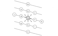
- the above pixels are arranged in a matrix. Accordingly, there are a large number of pixels in the upper, lower, left, and right diagonal directions around the processing target pixel (target pixel). Two or more comparison pixels are selected from pixels existing in the upper, lower, left, and right diagonal directions of these processing target pixels. For example, it is conceivable to select a pixel separated by one pixel on the left and three pixels on the right. When the pixel value of the target pixel is larger than the pixel value of the comparison pixel, noise reduction processing is usually performed assuming that the target pixel contains noise.
- the absolute value obtained by subtracting the pixel value of the comparison pixel from the pixel value of the target pixel is larger than a preset value. In such a case, if noise reduction processing is performed, an image with a blurred edge is obtained.
- the noise reduction processing device of the present invention is a noise reduction processing device that performs noise reduction processing on a video signal input to pixels arranged in a matrix according to the pixel value of the pixel,
- a noise amount calculating means for calculating a noise amount of the target pixel from an absolute value of a difference between the pixel value and an average value of the pixel values of a plurality of comparison pixels arranged in an arbitrary direction around the target pixel;
- the absolute value of the difference between the pixel value of the pixel of interest and the pixel values of a plurality of peripheral pixels arranged around the pixel of interest is a value corresponding to the noise amount calculated by the noise amount calculation means.
- At least one noise processing circuit having a counting means for counting the number of smaller peripheral pixels, and the number of peripheral pixels counted by the counting means is less than or equal to a preset number It performs noise reduction processing on the target pixel, when the number of the counted peripheral pixel is greater than the number set in advance, and characterized in that it does not perform the noise reduction process on the pixel of interest.
- the absolute value of the difference from the peripheral pixel is obtained, and the noise amount of the target pixel is calculated from the absolute value. Is calculated. Then, the absolute value of the difference between the pixel value of the pixel of interest and the pixel values of a plurality of peripheral pixels arranged around the pixel of interest is obtained from a value corresponding to the noise amount calculated by the noise amount calculation unit. If the number of smaller neighboring pixels is counted and the number of neighboring pixels counted is equal to or smaller than a preset number, the noise reduction processing is performed on the pixel of interest, and the pixel is on the pixel. After accurately determining whether or not the noise is a peak at a pixel in the edge portion of the video, noise reduction processing is performed on the pixel of interest.
- the noise reduction processing device of the present invention is a noise reduction processing device that performs noise reduction processing on a video signal input to pixels arranged in a matrix, and includes a pixel value of a target pixel to be processed and the target attention.
- a first difference calculation circuit for obtaining a difference from pixel values of peripheral pixels arranged around the pixel, and a difference obtained by the first difference calculation circuit for the number of peripheral pixels arranged around the pixel of interest. Is used as a unit, and when the determination pattern formed from the difference of one unit matches a determination reference pattern that is a determination reference for determining whether or not to perform the noise reduction processing, it is input to the target pixel.
- Noise reduction processing is performed on the video signal, and the determination pattern does not match the determination reference pattern, the video signal input to the target pixel It is characterized in that a first noise processing circuit is not executed noise reduction processing.
- the difference between the pixel value of the target pixel to be processed and the pixel values of the peripheral pixels arranged around the target pixel is equal to the number of peripheral pixels arranged around the target pixel.
- the determination pattern formed from the difference of one unit matches a determination reference pattern that is a determination reference for determining whether or not to perform the noise reduction processing, it is input to the target pixel.
- the noise reduction process is performed on the video signal and the determination pattern does not match the determination reference pattern, the noise reduction process is not performed on the video signal input to the target pixel.
- the determination reference pattern is set to a pattern that is highly likely to be determined as noise, the ability to discriminate between noise and video can be improved, so that the cause of noise can be determined appropriately. It becomes possible. That is, unnecessary noise reduction processing can be eliminated.
- noise reduction processing is performed using an adaptive low-pass filter
- the peak of the input waveform in the original video signal can be suppressed by unnecessary noise reduction processing, and noise can be reduced.
- the video after the reduction process is lost. That is, there is an effect that it is possible to provide a noise reduction processing apparatus that is more effective in reducing noise than the means of Patent Document 1 and that is less likely to produce a video.
- the present invention is a noise reduction processing device that performs noise reduction processing on a video signal input to pixels arranged in a matrix according to the pixel value of the pixel, and from the pixel value of the pixel of interest,
- the comparison pixels existing on both sides of the target pixel are not necessarily the same as the comparison pixel. If the difference between the obtained pixel values is less than or equal to a preset value, noise reduction processing is performed on the pixel of interest, and the obtained pixel value difference is greater than the preset value.
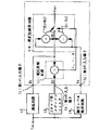
- FIG. 2 is a schematic configuration block diagram of an NR circuit in an image processing engine provided in the liquid crystal display device shown in FIG. 1.
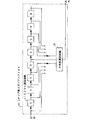
- FIG. 4 is a schematic configuration block diagram of the NR circuit shown in FIG. 3.
- FIG. 5 is a schematic block diagram showing details of the noise processing unit with the noise amount detection unit omitted in the NR circuit shown in FIG. 4. It is a graph for demonstrating the effect of this invention.
- FIG. 6 is a diagram showing an original image for explaining an effect in the first embodiment.
- FIG. 10 is a diagram illustrating a noise reduction process after illustrating an effect in the first embodiment. It is a figure which shows after the noise reduction process by the prior art as a comparative example for demonstrating the effect in Embodiment 1.
- FIG. It is a figure which shows the difference in the image after the noise reduction process by Embodiment 1 and the prior art as a comparative example.
- FIG. 6 is a block diagram schematically illustrating a configuration of an interdot noise processing circuit in an NR circuit according to a second embodiment.
- FIG. 6 is a block diagram of a schematic configuration of an inter-line noise processing circuit in an NR circuit according to a second embodiment. It is a figure which shows after the noise reduction process for demonstrating the effect in Embodiment 2.
- FIG. 6 is a block diagram schematically illustrating a configuration of an interdot noise processing circuit in an NR circuit according to a second embodiment.
- FIG. 6 is a block diagram of a schematic configuration of an inter-line noise processing circuit in an
- FIG. 17 is a schematic configuration block diagram of an NR circuit in an image processing engine provided in the liquid crystal display device shown in FIG. 16.
- (A)-(c) is a figure explaining the outline
- FIG. 25 is a diagram illustrating an outline of noise reduction processing in the NR circuit shown in FIG. 24.
- FIG. It is a figure which shows after the noise reduction process for demonstrating the effect in Embodiment 6.
- FIG. It is a figure which shows the noise reduction process after the prior art as a comparative example for demonstrating the effect in Embodiment 6.
- FIG. It is a figure which shows the difference in the image after the noise reduction process by Embodiment 6 and the prior art as a comparative example.
- (A) (b) is a figure for demonstrating the principle of the noise reduction process of this invention. It is a figure which shows the pattern for determination criteria used as the determination criterion which determines whether the noise reduction process used by the noise reduction process of this invention is performed.
- FIG. 30 is a block diagram schematically illustrating a configuration of an NR circuit in an image processing engine provided in the liquid crystal display device illustrated in FIG. 29.
- FIG. 33 is a schematic configuration block diagram of an NR arithmetic circuit included in the NR circuit shown in FIG. 32. It is a figure which shows the original image for demonstrating the effect in Embodiment 8.
- FIG. It is a figure which shows the result of having performed the noise reduction process only to the horizontal direction with the conventional method with respect to the original image shown in FIG.
- FIG. 35 is a diagram showing a result of noise reduction processing performed on the original image shown in FIG. 34 by the NR circuit shown in FIG. 32. It is a schematic block diagram of the NR circuit concerning Embodiment 9 of this invention.
- FIG. 33 is a schematic configuration block diagram of an NR arithmetic circuit included in the NR circuit shown in FIG. 32. It is a figure which shows the original image for demonstrating the effect in Embodiment 8.
- FIG. It is
- FIG. 38 is a schematic configuration block diagram of an NRBI circuit included in the NR circuit shown in FIG. 37.
- FIG. 39 is a block diagram of a schematic configuration of an NR interpolation arithmetic circuit included in the NRBI circuit shown in FIG. 38. It is a figure which shows an example of the interpolation filter used with the NR interpolation calculation circuit shown in FIG. It is a figure which shows the result of having applied the noise reduction process to the horizontal direction and the vertical direction with the conventional method with respect to the original image shown in FIG.
- FIG. 37 is a diagram illustrating a result of noise reduction processing performed on the original image illustrated in FIG. 34 by the NR circuit illustrated in FIG. It is a schematic block diagram of the NR circuit concerning Embodiment 10 of this invention.
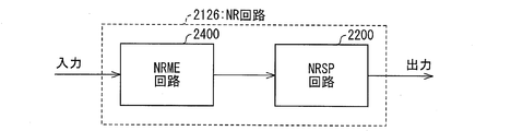
- FIG. 44 is a schematic configuration block diagram of an NRME circuit included in the NR circuit shown in FIG. 43.
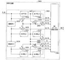
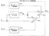
- FIG. FIG. 45 is a block diagram of a schematic configuration of an NR median arithmetic circuit included in the NRME circuit shown in FIG. 44. It is a figure which shows the pixel arrangement
- FIG. 1 is a block diagram showing the overall configuration of a liquid crystal display device 101 as a display device to which the noise reduction processing apparatus of the present invention is applied.
- the liquid crystal display device 101 includes a liquid crystal module 102 for displaying an image, an image processing engine 103 for supplying a video signal for display to the liquid crystal module 102, and the image processing engine 103. It has a configuration including at least a tuner 104 for detecting the supplied RF signal (video signal).
- a broadcast wave as the video signal.
- the broadcast wave signal system is an interlaced signal such as NTSC system or PAL system.
- the image processing engine 103 includes a Y / C separation circuit 105, an NR circuit (noise reduction processing device) 106, and an I / P conversion circuit 107, and performs predetermined processing on the detected RF signal (video signal). Then, it is sent to the subsequent liquid crystal module (display device) 102.
- the liquid crystal display device 101 detects an RF signal received from an antenna or a cable with the tuner 104 and sends a CVBS (composite video signal) to the image processing engine 103.
- the CVBS is separated into a luminance signal Y and a color signal C by the Y / C separation circuit 105.
- the NR circuit 106 removes noise from the YC signal and outputs it to the I / P conversion circuit 107.
- the I / P conversion circuit 107 converts the resolution of the input video in accordance with the resolution of the liquid crystal and outputs it to the liquid crystal module 102.
- the input video signal is received by a TCON (timing controller) 108, converted into a signal and timing according to the specifications of the LCD (liquid crystal panel) 109, and displayed on the LCD 109.
- the LCD 109 is a display panel (display unit) arranged in a matrix and having pixels corresponding to input image data.
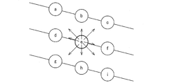
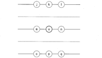
- comparison pixels are selected from the pixels existing in the upper, lower, left, and right diagonal directions of these processing target pixels, and will be described below as comparison pixels. Note that FIG. 2 seems to select a comparison pixel from eight pixels around the pixel of interest, but another pixel may be sandwiched between them.
- whether or not noise is present on the processing target pixel e is determined by whether or not the processing target pixel e has a peak compared to the comparison pixels a to d and f to i.
- the processing target pixel e It is determined that noise is present on e, and noise reduction processing is performed. For this reason, the part that is originally displayed as the edge of the video is blurred by the noise reduction processing, and the entire video is made to feel lost.
- whether or not noise is present on the processing target pixel e is determined based on whether the processing target pixel e has a peak compared to the comparison pixels a to d and f to i. Judgment is also made using the relationship.
- the NR circuit 106 when the absolute value of the difference between the pixel value of the processing target pixel e and the pixel values of the comparison pixels a to d and f to i is larger than a preset value, It is determined that the pixel value of the pixel e has a peak compared to the pixel values of the comparison pixels a to d and f to i. Then, the following determination is further performed while satisfying this condition.
- the pixels d and f are used as the comparison target pixels of the processing target pixel e, it is also checked whether or not the absolute value of the difference between the pixel values of the pixels d and f is larger than a preset value. It may be checked whether the absolute value of the difference between the pixel values of the pixels b and h is larger than a preset value.
- the pixel e When the difference between the pixel values of the pixels d and f is larger than a preset value, the pixel e has a peak (greater than or smaller than either of the pixels d and f) with respect to the pixels d and f. In this case, the noise reduction processing is not performed and the data is output to the subsequent I / P conversion circuit 107 as it is.
- noise reduction processing is performed if the pixel e has a peak with respect to the pixels d and f.
- the NR circuit 106 for executing the noise reduction processing has a configuration in which at least three types of noise processing circuits are connected in series.
- the inter-frame noise processing circuit 210 the inter-dot noise processing circuit 220, in order from the input side (in) to the output side (out),
- the inter-line noise processing circuit 230 is connected in series.
- the inter-frame noise processing circuit 210 includes a noise processing unit 211, a frame memory (FDL) 212, a frame memory (FDL) 213, and a noise amount detection unit 214, and performs noise removal by correlation between frames. ing.
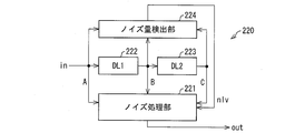
- the inter-dot noise processing circuit 220 includes a noise processing unit 221, a latch (DL1) 222, a latch (DL2) 223, and a noise amount detection unit 224, and performs noise removal by correlation between dots in the horizontal direction. It has become.
- the number of latches in the latch (DL1) 222 and the latch (DL2) 223 is variable in the range of about 1 to 5 latches, there is no problem in terms of function. Therefore, the number of latches in the latch (DL1) 222 and the latch (DL2) 223, that is, the number of stages may not be the same.
- the inter-line noise processing circuit 230 includes a noise processing unit 231, a line memory (HDL1) 232, a line memory (HDL2) 233, and a noise amount detection unit 234, and performs noise removal by correlation between lines in the vertical direction. It is like that.
- the number of lines in the line memory (HDL1) 232 and the line memory (HDL2) 233 is variable in the range of about 1 to 5 lines, there is no problem in terms of function. For this reason, the number of lines in the line memory (HDL1) 232 and the line memory (HDL2) 233, that is, the number of stages may not be the same.
- multistage noise processing is performed using three types of noise processing circuits. For example, it is possible to reduce only noise with a high probability and eliminate unnecessary noise reduction processing for the video.
- the noise between the frames of the video is removed by the inter-frame noise processing circuit 210, and the horizontal direction of the video subjected to the inter-frame noise processing by the inter-dot noise processing circuit 220.
- noise is removed by the correlation between dots, and noise is removed by the correlation between lines in the vertical direction of the image subjected to the inter-dot noise processing by the inter-line noise processing circuit 230. It becomes multifaceted, and it is possible to more reliably determine whether it is video or noise.
- noise amount detection units 214, 224, and 234 provided in each noise processing circuit.
- FIG. 4 shows a schematic block diagram of the interdot noise processing circuit 220.
- the noise amount detection unit 224 aggregates the absolute value distribution of the difference between the average values of the processing target pixel B and the comparison target pixels A and C over one frame period. The difference where the frequency is maximum is detected as the amount of noise.
- the noise amount detected by the noise amount detection unit 224 is sent to the noise processing unit 221 as nlv.
- FIG. 5 shows a schematic block diagram of the inter-dot noise processing circuit 220 shown in FIG. 4 with the noise amount detection unit 224 omitted.
- the video signal input from in is input to the latch (DL1) 222 and the latch (DL2) 223 as two delay circuits, Input to the noise processing unit 221.
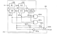
- the noise processing unit 221 includes a pixel value comparison unit for comparing pixel values, three comparison circuits 221a, 221b, and 221c as pixel value calculation units for calculating pixel values, and two as determination units. AND circuits 221d and 221e, an adder 221f, a subtractor 221g, and two switches 221h and 221i are provided.
- the comparison circuit 221a determines whether or not the pixel value of the processing target pixel B and the pixel value of the comparison pixel A have a relationship of A ⁇ B.
- a ⁇ B a high level signal is sent to each of the AND circuits 221d and 221f
- a ⁇ B a low level signal is sent to each of the AND circuits 221d and 221f.
- the comparison circuit 221b determines whether or not the pixel value of the processing target pixel B and the pixel value of the comparison target pixel C have a relationship of B ⁇ C.
- B ⁇ C a high level signal is sent to each of the AND circuits 221d and 221f, while when B ⁇ C, a low level signal is sent to each of the AND circuits 221d and 221f.
- the comparison circuit 221c determines whether the relationship between the pixel values of the comparison target pixels A and C adjacent to both sides of the processing target pixel B is C ⁇ A or C >> A. That is, it is determined whether the difference between the pixel values of the comparison target pixels A and C is large, that is, whether the absolute value of the difference is larger than a preset value. If C ⁇ A or C >> A, a high-level signal is sent to each of the AND circuits 221d and 221f, while C ⁇ A or C >> A is not satisfied. Sends a low level signal to each of the AND circuits 221d and 221f.
- the video signal output from the latch (DL1) 222 is sent to the wiring connected to the adder 221f and the subtracter 221g, and is connected to the wiring not connected to either the adder 221f or the subtracter 221g. And is output as an output signal (out) from any of the wirings.
- the above-described wiring switching is performed by switching the above-described switches 221h and 221i. Normally, the switches 221h and 221i are in a position for conducting a wire to which neither the adder 221f nor the subtracter 221g is connected.
- the switch 221h switches to the wiring connected to the subtracter 221g.
- the switch 221i switches to the wiring connected to the adder 221f when the signal output from the AND circuit 221e is at a high level.
- the AND circuit 221d receives a high level signal (a signal indicating A ⁇ B) from the comparison circuit 221a, a low level signal (a signal indicating B ⁇ C) from the comparison circuit 221b, and a low level signal from the comparison circuit 221c. Only when a signal (a signal indicating that neither C ⁇ A nor C >> A) is input, a high-level signal is output.
- the pixel value of the processing target pixel B is larger than the pixel value of the comparison target pixel A, but is equal to or larger than the pixel value of the comparison target pixel C, and the absolute value of the difference between the pixel values of the comparison target pixels A and C Is smaller than a preset value. That is, since it can be determined that a positive amount of noise is on the processing target pixel B, the noise amount nlv detected by the noise amount detection unit 224 is subtracted from the pixel value of the processing target pixel B.
- the AND circuit 221e receives a low level signal (a signal indicating A ⁇ B) from the comparison circuit 221a, and a high level signal (a signal indicating B ⁇ C) from the comparison circuit 221b from the comparison circuit 221c.
- a high-level signal is output only when a low-level signal (a signal indicating that neither C ⁇ A nor C >> A) is input.
- the pixel value of the processing target pixel B is the same as or smaller than the pixel value of the comparison target pixel A, smaller than the pixel value of the comparison target pixel C, and the absolute value of the difference between the pixel values of the comparison target pixels A and C is It indicates that the value is smaller than a preset value. That is, since it can be determined that a negative amount of noise is on the processing target pixel B, the noise amount nlv detected by the noise amount detection unit 224 is added to the pixel value of the processing target pixel B.
- the noise processing unit 221 configured as described above, if the signal from the comparison circuit 221c is at a high level, the signals output from the AND circuits 221d and 221e are related to the signals from the other comparison circuits 221a and 221b. Therefore, even if it is determined that noise is present on the processing target pixel B, it is determined that the noise indicates an edge portion, and noise reduction processing is performed on the video signal. It is designed to output as it is without being applied.
- the inter-dot noise processing circuit 220 including the noise processing unit 221 having the above configuration even when the processing target pixel B has a peak (maximum or minimum) with respect to the comparison target pixels A and C, If there is a large difference between the processing target pixels A and C, the noise reduction processing is not performed, so the situation where the noise reduction processing is erroneously performed on the pixels placed on the edge of the video and the video is lost Can be avoided.
- FIG. 6 shows the original signal (video signal with noise), the result of applying noise reduction processing to the original signal by the conventional method (conventional example), and the noise reduction processing of the present invention for the original signal. It is a graph which shows as a result (this invention) which gave.
- the line of the present invention shows the result when the noise reduction processing is not performed when the difference between the pixel values of the pixels A and C exceeds three times the noise amount nlv.
- the line of the conventional example does not depend on the difference between the processing target pixels A and C, and the noise reduction processing is performed when the processing target pixel B has a peak with respect to the comparison target pixels A and C. The result of having performed is shown.
- the noise reduction processing is not performed in the present invention, but the noise reduction processing is performed in the conventional example.
- the noise amount detected by the noise amount detection unit 224 described above is about 8/256, and the difference between the pixel values of the pixels A and C is about 6 to 10 in the drawing. Looks like there ’s no big difference.
- the above processing is sequentially performed in three directions, ie, the frame direction, the horizontal direction, and the vertical direction as in the NR circuit 106 shown in FIG.
- FIG. 7 shows a video (original image) with noise.
- FIG. 10 shows a video obtained by taking a difference between the video shown in FIG. 8 and the video shown in FIG.
- the edge portion is not determined to be noise and noise reduction processing is not performed, and in FIG. 9, the edge portion is determined to be noise and noise reduction processing is performed. I understand that.
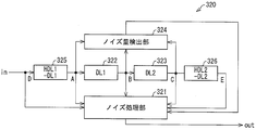
- a first noise reduction processing device in which the interdot noise processing circuit 220 of the NR circuit 106 shown in FIG. 3 of the first embodiment is replaced with the interdot noise processing circuit 320 shown in FIG.
- a second noise reduction processing apparatus in which the inter-line noise processing circuit 230 of the NR circuit 106 is replaced with the inter-line noise processing circuit 330 shown in FIG. 12 will be described.
- the inter-dot noise processing circuit 320 includes a noise processing unit 321, a latch (DL 1) 322, a latch (DL 2) 323, and a noise amount detection unit 324, and further includes an inter-dot dot differencer 325, a line
- the inter-dot difference unit 326 is included.
- the latch (DL1) 322, the latch (DL2) 323, and the noise amount detection unit 324 are the same as the respective units of the inter-dot noise processing circuit 220 of the NR circuit 106 shown in FIG. 3 of the first embodiment. Omitted.
- the line dot difference units 325 and 326 output data delayed by a predetermined number of lines to the noise processing unit 321, respectively.
- the latch (DL1) 322 and the latch (DL2) 323 output data delayed by a predetermined number of dots to the noise predetermined unit 321.
- the noise processing unit 321 uses a difference between lines (vertical direction) even when performing noise processing between dots (horizontal direction).
- the processing target pixel B has a peak with respect to the comparison target pixels A and C, if there is a large difference between the pixel values of the comparison target pixels A and C, the noise reduction processing is not performed. Furthermore, if there is a large difference between the pixel values of the inter-line pixels D and E, the noise reduction process is not performed.
- the inter-line noise processing circuit 330 includes a noise processing unit 331, a latch (DL1) 332, a latch (DL2) 333, and a noise amount detection unit 334, and further includes an inter-line dot differencer 335, a line
- the inter-dot difference unit 336 is provided.
- the latch (DL1) 332 and the line dot differencer 335 constitute a line memory HDL1
- the latch (DL2) 333 and the line dot differencer 336 constitute a line memory HDL2.
- the line-dot difference units 335 and 336 output data delayed by a predetermined number of lines to the noise processing unit 331, respectively. Further, the latch (DL1) 332 and the latch (DL2) 333 output data delayed by a predetermined number of dots to the noise processing unit 331.
- the noise processing unit 331 uses a difference between dots (horizontal direction) even when performing noise processing between lines (vertical direction).
- the noise reduction processing is not performed if there is a large difference between the comparison target pixels D and E. Furthermore, if there is a large difference between the pixels A and C between the lines, the noise reduction process is not performed.
- FIG. 13 shows the result of applying the noise reduction processing described in the second embodiment to the video (original image) in which noise in FIG. 7 is placed.
- FIG. 14 shows the difference between the image shown in FIG. 13 and the image subjected to the conventional noise reduction processing of FIG. Also from the video shown in FIG. 14, it can be seen that the video shown in FIG. 13 is a video in which noise is reduced and the detail is not reduced as compared with the video that has been subjected to the conventional noise reduction processing. .
- the video shown in FIG. 13 is clearer than the video shown in FIG. 8 showing the result of the first embodiment.
- the noise reduction processing of the second embodiment has reduced the video detail more than the noise reduction processing of the first embodiment.
- the inter-frame noise processing circuit 210, the inter-dot noise processing circuit 220 (320), and the inter-line noise processing circuit 230 (330) are arranged in this order from the input side to the output side. Connected in series.
- the order of connection is not limited, and the interframe noise processing circuit 210, the interdot noise processing circuit 220 (320), and the interline noise processing circuit 230 (330) may be connected in series in any order. Further, any processing circuit may be missing, or only one processing circuit may be provided.
- the inter-frame noise processing circuit 210, the inter-dot noise processing circuit 220 (320), and the inter-line noise processing circuit 230 (330) is changed.
- the arrangement of the inter-frame noise processing circuit 210, the inter-dot noise processing circuit 220 (320), and the inter-line noise processing circuit 230 (330) constituting the NR circuit 106 in the first and second embodiments is changed. The case will be described.
- the inter-line noise processing circuit 230 (330) is arranged last, the horizontal line is less noticeable and the vertical line is more noticeable.
- the inter-line noise processing circuit 230 (330) at the end, the horizontal lines in the video are less noticeable and the vertical lines are more noticeable, which is effective in the case where noise is present on the horizontal lines of the video. It is. In analog broadcasting, since noise is generated continuously for a certain period of time, it tends to be horizontal noise.
- the inter-dot noise processing circuit 220 (320) is arranged last, the vertical line is less noticeable and the horizontal line is more noticeable.
- the inter-dot noise processing circuit 220 (320) at the end, the vertical lines in the video are less noticeable and the horizontal lines are more noticeable, which is effective when there are originally many horizontal lines in the video.
- the inter-frame noise processing circuit 210 does not cause any particular problems even if it is arranged last like the inter-line noise processing circuit 230 (330) or the inter-dot noise processing circuit 220 (320). However, since flicker does not occur when noise between frames is first reduced, it is preferable that the inter-frame noise processing circuit 210 is arranged first.
- the inter-frame noise processing circuit 210 when performing inter-dot noise processing and inter-line noise processing in the subsequent stage, it can be performed on an image without flicker. It is possible to more accurately determine whether or not it is placed.
- the inter-frame noise processing circuit 210 is first arranged, and the arrangement positions of the remaining noise processing circuits may be appropriately determined in accordance with the noise tendency of the video signal.
- the noise processing circuit may have the following circuit configuration.
- the noise processing circuit includes a pixel value comparison unit that compares a pixel value of a target pixel and a pixel value of a comparison pixel that is present in an oblique direction of the target pixel, and a comparison result by the pixel value comparison unit indicates that the target pixel
- a pixel value calculation unit that obtains a difference between pixel values of both sides of the target pixel when the pixel value of the target pixel is larger or smaller than any of the pixel values of the plurality of comparison pixels of the target pixel
- a determination unit that determines whether or not to perform noise reduction processing on the pixel of interest from a calculation result by the pixel value calculation unit, wherein the determination unit sets a difference in pixel value between the pixels on both sides in advance. If the difference between the obtained pixel values is larger than a preset value, the noise reduction process is not performed on the target pixel. In the configuration to judge That.
- a noise amount detection circuit that detects a noise amount generated in the target pixel from the pixel value of the target pixel and the pixel value of the comparison pixel of the target pixel is provided, and the noise processing circuit includes: When it is determined that noise reduction processing is performed on the target pixel, it is preferable to add or subtract the noise amount detected by the noise amount detection circuit from the pixel value of the target pixel.
- the detected amount of noise for the pixel value of the target pixel is calculated.
- Noise reduction processing can be performed simply by adding and subtracting.
- the noise reduction processing device of the present invention is a noise reduction processing device that performs noise reduction processing on a video signal input to pixels arranged in a matrix according to the pixel value of the pixel, An inter-frame noise processing circuit that performs noise processing for each frame, an inter-dot noise processing circuit that performs noise processing in the horizontal direction of the video signal, and an inter-line noise processing circuit that performs noise processing in the vertical direction of the video signal,
- the noise processing circuit of the noise reduction processing device according to any one of claims 1 to 3, wherein the inter-frame noise processing circuit, the inter-dot noise processing circuit, and the inter-line noise processing circuit are connected in series. It is characterized by that.
- noise processing such as the inter-frame noise processing circuit, the inter-dot noise processing circuit, and the inter-line noise processing circuit are sequentially performed.
- the inter-frame noise processing circuit the inter-dot noise processing circuit
- the inter-line noise processing circuit the inter-line noise processing circuit
- the inter-dot noise processing circuit determines whether to perform the noise processing in the horizontal direction using the difference between the comparison pixels between the lines arranged in the vertical direction.
- the inter-dot noise processing circuit determines whether to perform noise processing by determining whether to perform horizontal noise processing using the difference between lines arranged in the vertical direction.
- the determination uses not only the difference between the dots but also the difference between the lines arranged in the vertical direction.
- the inter-line noise processing circuit determines whether to perform noise processing in the vertical direction using a difference between inter-dot comparison pixels arranged in the horizontal direction.
- the inter-line noise processing circuit determines whether to perform noise processing by determining whether to perform noise processing in the vertical direction using a difference between dots arranged in the horizontal direction.
- the determination uses not only the difference between lines but also the difference between dots arranged in the horizontal direction.
- the unnecessary noise reduction process for the target pixel is not performed by checking the difference between the dots.
- the target pixel is B, the pixels D and E between the dots, and the pixels A and C between the lines, if the target pixel B has a peak with respect to the pixels D and E, However, when the absolute value of the difference between the pixel values of the pixels A and C is larger than a preset value, the target pixel B is not noise, and Noise reduction processing is not performed.
- inter-frame noise processing circuit inter-dot noise processing circuit
- inter-line noise processing circuit it is preferable that the inter-line noise processing circuit is connected last.
- the horizontal lines in the video are less noticeable and the vertical lines are more noticeable, which is effective in the case where noise is placed on the horizontal lines of the video.
- the inter-dot noise processing circuit is preferably connected last.
- the vertical lines in the video are less noticeable and the horizontal lines are more noticeable, which is effective when there are originally many horizontal lines in the video.
- inter-frame noise processing circuit As the above-mentioned inter-frame noise processing circuit, inter-dot noise processing circuit, and inter-line noise processing circuit, it is preferable that the inter-frame noise processing circuit is connected first.
- the display device of the present invention includes pixels arranged in a matrix, and displays a video based on a supplied video signal, and the pixel value of the pixel with respect to the video signal input to the pixel And a noise reduction processing device that performs noise reduction processing in accordance with the noise reduction processing device having the above configuration as the noise reduction processing device, the display device has less noise. In addition, it is possible to display an image with high display quality with little loss.
- FIG. 16 is a block diagram showing the overall configuration of a liquid crystal display device 1101 as a display device to which the noise reduction processing apparatus of the present invention is applied.
- the liquid crystal display device 1101 includes a liquid crystal module 1102 for displaying an image, an image processing engine 1103 for supplying a video signal for display to the liquid crystal module 1102, and the image processing engine 1103. It has a configuration including at least a tuner 1104 for detecting a supplied RF signal (video signal).
- a broadcast wave as the video signal.
- the broadcast wave signal system is an interlaced signal such as NTSC system or PAL system.
- the image processing engine 1103 includes a Y / C separation circuit 1105, an NR circuit (noise reduction processing device) 1106, and an I / P conversion circuit 1107, and performs predetermined processing on the detected RF signal (video signal). And sent to the liquid crystal module (display device) 1102 in the subsequent stage.
- the liquid crystal display device 1101 detects an RF signal received from an antenna or a cable with the tuner 1104 and sends a CVBS (composite video signal) to the image processing engine 1103.
- the CVBS is separated into a luminance signal Y and a color signal C by a Y / C separation circuit 1105.
- the NR circuit 1106 removes noise from the YC signal and outputs it to the I / P conversion circuit 1107.
- the I / P conversion circuit 1107 converts the resolution of the input video in accordance with the resolution of the liquid crystal and outputs it to the liquid crystal module 1102.
- the input video signal is received by a TCON (timing controller) 1108, converted into a signal and timing conforming to the specification of the LCD (liquid crystal panel) 1109, and displayed on the LCD 1109.
- the LCD 1109 is a display panel (display unit) arranged in a matrix and having pixels corresponding to input image data.
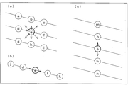
- peripheral pixels As peripheral pixels of the processing target pixel e, eight pixels a to d, f to i adjacent to the processing target pixel e, and four pixels j, k, m, n.
- whether or not noise is present in the processing target pixel e is determined by whether or not the processing target pixel e has a peak compared to the neighboring peripheral pixels a to d and f to i.
- the noise reduction processing for the processing target pixel e cannot be performed appropriately.
- the treatment target pixel e is a pixel at the edge portion of the video, it naturally has a peak compared to the surrounding pixels.
- noise reduction processing is performed on the pixels of the edge portion of the video that originally does not require noise reduction processing, and the entire video feels lost.
- the processing target pixel e it is examined by the following method whether or not the reason why the processing target pixel e has a peak compared to the peripheral pixels a to d, f to i, j, k, m, and n is due to noise alone. .
- the image signal Ex of the eight peripheral pixels should have a difference of about the noise amount Nd from the image signal E9 of the processing target pixel e. That is, if the absolute values Fx of the eight differences are all about the noise amount Nd, it can be said that noise is the only cause of the processing target pixel e having a peak.
- the absolute value Fx of the eight differences is less than the Y value (Y is an integer of 1 to 3) that is smaller than the noise amount Nd, it is determined that the processing target pixel e has noise. Then, noise reduction processing is performed on the processing target pixel e.
- the absolute value Fx of the eight differences has a value smaller than the noise amount Nd larger than the preset Y values (Y is an integer of 1 to 3), it is determined that no noise is placed on the processing target pixel e. However, noise reduction processing is not performed on the processing target pixel e.
- the noise reduction processing performed in the present invention is performed by comparing the processing target pixel e with a set of horizontal peripheral pixels j and k centered on the processing target pixel e or a set of horizontal peripheral pixels d and f. If the processing target pixel e has a peak, the noise amount Nd is adjusted from the processing target pixel e. In addition, the processing target pixel e has a peak compared with the set of the peripheral pixels m and n in the vertical direction around the processing target pixel e or the set of the peripheral pixels b and h in the vertical direction. If so, the noise amount Nd is adjusted from the processing target pixel e.
- the noise reduction processing that hardly crushes the contour is realized by the addition / subtraction processing of the noise amount Nd.
- ⁇ Noise reduction processing device> The noise reduction process is realized by the NR circuit 1106 shown in FIG.
- FIG. 18 is a schematic configuration block diagram of the NR circuit 1106.
- the NR circuit 1106 includes a pixel value of a processing target pixel (target pixel) and a plurality of comparison target pixels (horizontal pixels centered on the processing target pixel among peripheral pixels).
- the horizontal NR processing circuit (horizontal noise processing circuit) 1210 that performs noise reduction processing in the horizontal direction of the processing target pixel from the comparison with the pixel value of the comparison pixel) and the horizontal NR processing circuit 1210 Pixel value of a processing target pixel that has been subjected to noise reduction processing in the direction or processing target pixel that has not been subjected to noise reduction processing, and pixel values of a plurality of comparison pixels that are arranged in the vertical direction centering on the processing target pixel From the comparison, a vertical NR processing circuit (vertical noise processing circuit) 1220 for performing noise reduction processing in the vertical direction of the pixel to be processed is provided.
- the horizontal NR processing circuit 1210 includes a first histogram processing unit (first noise amount calculation unit) 1211, a first count unit (first count unit) 1212, and a first addition / subtraction unit (first noise processing unit) 1213. Yes.
- the first histogram processing unit 1211 includes an image signal (pixel value) of the processing target pixel e and a plurality of pixels (comparison pixels ((b) in FIG. 19) arranged in the horizontal direction centering on the processing target pixel e.
- the absolute value of the difference is histogrammed over one frame, and the mode value is used as the noise amount Nd.
- the first count unit 1212 includes an image signal of the processing target pixel e, and a plurality of peripheral pixels (pixels a to d and f to i shown in FIG. 19A) arranged around the processing target pixel e.
- the first counting unit 1212 determines that the processing target pixel e is subjected to noise reduction processing.
- the first addition / subtraction unit 1213 is informed of the target pixel, that is, A ⁇ Y.
- the first addition / subtraction unit 1213 performs the following noise reduction processing when A ⁇ Y, but does not perform noise reduction processing when A> Y. That is, in this case, the noise reduction processing for the processing target pixel e in the horizontal NR processing circuit 1210 is not performed.
- the first addition / subtraction unit 1213 compares the processing target pixel e with the comparison pixels (pixels d, f, j, k), and uses the image signals of all the comparison pixels compared with the image signals of the processing target pixel e. Is larger, the value corresponding to the noise amount Nd calculated by the first histogram processing unit 1211 is subtracted from the image signal of the processing target pixel e, and all the image signals of the processing target pixel e are compared. When it is smaller than the image signal of the comparison pixel, a process of adding a value corresponding to the noise amount Nd calculated by the first histogram processing unit 1211 from the image signal of the processing target pixel e is performed. Further, when the above condition is not satisfied and when A> Y, noise reduction processing is not performed.
- the vertical NR processing circuit 1220 includes a second histogram processing unit (second noise amount calculation unit) 1221, a second count unit (second count unit) 1222, and a second addition / subtraction unit (second noise processing unit) 1223. I have.
- the second histogram processing unit 1221 includes an image signal (pixel value) of the processing target pixel e and a plurality of pixels (comparison pixels ((c) in FIG. 19) arranged in the vertical direction centering on the processing target pixel e.
- the absolute value of the difference is histogrammed over one frame, and the mode value is set as the noise amount Nh.
- the second count unit 1222 includes the image signal of the processing target pixel e and a plurality of peripheral pixels (pixels a to d and f to i shown in FIG. 19A) arranged around the processing target pixel e. ) Counts the number B of peripheral pixels in which the absolute value of the difference from the image signal is smaller than the value corresponding to the noise amount Nh calculated by the second histogram processing unit 1221.
- the second count unit 1222 determines that the processing target pixel e is subjected to noise reduction processing.
- the second addition / subtraction unit 1223 is informed of the target pixel, that is, B ⁇ Y.
- the second addition / subtraction unit 1223 performs the following noise reduction processing when B ⁇ Y, but does not perform noise reduction processing when B> Y. That is, in this case, the noise reduction processing for the processing target pixel e in the vertical NR processing circuit 1220 is not performed.
- the second addition / subtraction unit 1223 compares the processing target pixel e with the comparison pixels (pixels b, h, m, n shown in (c) of FIG. 19), When the image signal of the processing target pixel e is larger than the image signals of all the comparison pixels compared, this corresponds to the noise amount Nh calculated by the second histogram processing unit 1221 from the image signal of the processing target pixel e. When the value is subtracted and the image signal of the processing target pixel e is smaller than the image signals of all the comparison pixels compared, the second histogram processing unit 1221 calculates the image signal of the processing target pixel e. A process of adding a value corresponding to the noise amount Nh is performed. Further, when the above condition is not satisfied and when B> Y, noise reduction processing is not performed.
- the NR circuit 1106 performs processing by the horizontal NR processing circuit 1210 as the first step, and performs processing by the vertical NR processing circuit 1220 as the second step.
- the absolute value F9 of the difference between the average value of the image signals E4 and E5 of the pixels d and f and the image signal E9 of the processing target pixel e is obtained.
- the absolute value F9 of this difference is histogrammed over one frame, and the mode value is set as the noise amount Nd.
- the set of pixels and the processing target pixel e are compared.
- pixels d and f that are one pixel apart in the horizontal direction from the processing target pixel e correspond to pixels j and k that are two pixels apart.
- the amount of noise Nd is added from the image signal E9.
- noise reduction processing vertical NR processing circuit
- the noise amount Nh is determined based on the average value of the image signals E2 and E7 of the pixels b and h arranged in the vertical direction around the processing target pixel e and the processing target pixel e. It is obtained from the absolute value F10 of the difference from the image signal E9.
- FIG. 20 shows a video (original image) with noise.
- FIG. 23 shows an image showing the result of multiplying the difference between the image shown in FIG. 21 and the image shown in FIG. 22 by eight times.
- the arrangement of the horizontal NR processing circuit 1210 and the vertical NR processing circuit 1220 shown in FIG. 18 is reversed, and the pixel value of the processing target pixel (target pixel) and the peripheral pixels
- the noise reduction processing in the vertical direction of the processing target pixel is performed by comparing with the pixel values of a plurality of comparison target pixels (hereinafter referred to as comparison pixels) arranged in the vertical direction around the processing target pixel.
- a horizontal NR processing circuit 121 that performs noise reduction processing in the horizontal direction of the processing target pixel based on comparison with pixel values of a plurality of comparison pixels arranged in the center in the horizontal direction. It will be provided with a door.
- one of the noise processing circuits may be arranged in the preceding stage according to the type of image (video) that each noise processing circuit is good at.
- the image signals of the pixels in the horizontal direction and the vertical direction are used.
- the present invention is not limited to this, and the pixels in the time axis direction are used. These image signals may be used.
- Embodiment 6 an example of a noise reduction processing device that performs noise reduction processing using an image signal of a pixel in the time axis direction will be described.
- time NR processing circuit time-axis direction noise processing circuit 1230 shown in FIG. 24 is further provided in the NR circuit 1106 shown in FIG. 18 of the fourth embodiment.
- time NR processing circuit 1230 is provided before the horizontal NR processing circuit 1210 and the vertical NR processing circuit 1220 described in the fourth embodiment. In this embodiment, an example in which the time NR processing circuit 1230 is provided in the preceding stage of the horizontal NR processing circuit 1210 will be described.
- time NR processing circuit 1230 will be described below with reference to FIGS.
- the time NR processing circuit 1230 includes a third histogram processing unit (third noise amount calculation unit) 1231, a third count unit (third count unit) 1232, and a third addition / subtraction unit (third noise processing). Means) 1233.
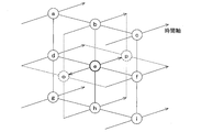
- the third histogram processing unit 1231 includes an image signal of the processing target pixel e and a plurality of pixels (comparison pixels: pixels shown in FIG. 25) arranged one frame apart in the time axis direction centering on the processing target pixel e.
- the absolute value of the difference between the average value of the pixel signals o, p) and the image signal of the processing target pixel e is converted into a histogram to calculate the amount of noise.
- the absolute value of the difference is histogrammed over one frame, and the mode value is used as the noise amount Nf.
- the third count unit 1232 includes the pixel value of the processing target pixel e and the image signals of a plurality of peripheral pixels (pixels a to d and f to i shown in FIG. 25) arranged around the processing target pixel e.
- the number C of neighboring pixels in which the absolute value of the difference between the two is smaller than the value corresponding to the noise amount Nf calculated by the third histogram processing unit 1231 is counted.
- the third counting unit 1232 determines that the processing target pixel e is subjected to noise reduction processing.
- the third addition / subtraction unit 1233 is informed of the target pixel, that is, C ⁇ Y.
- the third addition / subtraction unit 1233 performs the following noise reduction processing when C ⁇ Y, but does not perform noise reduction processing when C> Y. That is, in this case, the noise reduction processing for the processing target pixel e in the time NR processing circuit 1230 is not performed.
- the third addition / subtraction unit 1233 compares the processing target pixel e with the comparison pixels (pixels o and p shown in FIG. 25), and based on the image signals of all the comparison pixels compared with the image signal of the processing target pixel e. Is larger, the value corresponding to the noise amount Nf calculated by the third histogram processing unit 1231 is subtracted from the image signal of the processing target pixel e, and all the image signals of the processing target pixel e are compared. When the image signal is smaller than the image signal of the comparison pixel, a process of adding a value corresponding to the noise amount Nf calculated by the third histogram processing unit 1231 from the image signal of the processing target pixel e is performed. Further, when the above condition is not satisfied and when C> Y, the noise reduction process is not performed.
- the processing target pixel e and the pixels o and p in the time axis direction not only the processing target pixel e and the pixels o and p in the time axis direction but also the processing target pixel e and the peripheral pixels a to d and f to i are compared. Also do.
- the absolute value F11 of the difference between the average value of the image signals E11 and E12 of the pixels o and p, which is the frame data before and after the position of the processing target pixel e, and the image signal E9 of the processing target pixel e is obtained.
- the absolute value F11 of the difference is histogrammed over one frame, and the mode value is set as the noise amount Nf.
- the noise amount Nf is subtracted from the image signal E9 of the processing target pixel e.
- the noise amount Nf is added from the image signal E9 of the processing target pixel e.
- horizontal NR processing by the horizontal NR processing circuit 1210 and vertical NR processing by the vertical NR processing circuit 1220 shown in the fourth embodiment are performed.
- FIG. 26 shows a result of applying the noise reduction processing described in the second embodiment to the video (original image) in which noise of FIG. 20 used in the description of the fourth embodiment is present. .
- FIG. 27 shows the result of performing noise reduction processing in the time axis direction, horizontal direction, and vertical direction by conventional noise reduction processing, as in the sixth embodiment.
- FIG. 28 shows an image showing the result of multiplying the difference between the image shown in FIG. 26 and the image shown in FIG. 27 by eight times.
- the time NR processing circuit 1230 by providing the time NR processing circuit 1230, it is possible to perform noise reduction processing in consideration of the pixel value of the processing target pixel e that changes in units of frames.
- the time NR processing circuit 1230 since the result of the noise processing in the time axis direction by the time NR processing circuit 1230 is most difficult to produce, for example, in the case of a still image, the position of the edge does not change much in the time direction, and images of the same edge can be compared. Therefore, it becomes difficult to crush the edges, and as a result, blurring is less likely to occur.
- the time NR processing circuit 1230 is provided in the preceding stage of the horizontal NR processing circuit 1210 .
- the present invention is not limited to this example, and the vertical NR processing circuit 1230 is not limited thereto.
- the time NR processing circuit 1230 may be provided in the preceding stage of the vertical NR processing circuit 1220.
- an example in which a time NR processing circuit 1230 is provided in the preceding stage of the vertical NR processing circuit 1220 when processing is performed in the order of the vertical NR processing circuit 1220 and the horizontal NR processing circuit 1210 will be described.
- the time NR processing circuit 1230 precedes the vertical NR processing circuit 1220 with respect to the arrangement direction of the vertical NR processing circuit 1220 and the horizontal NR processing circuit 1210 in the fifth embodiment. Is arranged. Accordingly, the vertical NR processing circuit 1220 uses the pixel value output from the time NR processing circuit 1230 as the pixel value of the processing target pixel.
- the vertical NR processing circuit 1220 is arranged in the preceding stage of the horizontal NR processing circuit 1210, and the time NR processing circuit 1230 is arranged in the preceding stage of the vertical NR processing circuit 1220, so that the same effect as in the sixth embodiment is obtained. Can be played.
- time NR processing circuit 1230 is preferably arranged in front of the horizontal NR processing circuit 1210 and the vertical NR processing circuit 1220 in order to eliminate edge blurring because it is difficult to crush edges.
- only the horizontal NR processing circuit 1210, only the vertical NR processing circuit 1220, or only the time NR processing circuit 1230 may be used after the noise reduction processing as compared with the prior art. Don't make money.
- a horizontal NR processing circuit 1210 As a configuration that hardly causes edge blurring, as in the sixth and seventh embodiments, there are three types of noise processing circuits: a horizontal NR processing circuit 1210, a vertical NR processing circuit 1220, and a time NR processing circuit 1230. This is the case.
- a horizontal NR processing circuit 1210 and a vertical NR processing circuit 1220 may be used in order to suppress costs and prevent a certain amount of edge blurring.
- the noise reduction process in the noise processing circuit compares the target pixel with a plurality of comparison pixels arranged in an arbitrary direction, and the pixel value of the target pixel is larger than the pixel values of all the comparison pixels
- this is a process of adding a value corresponding to the noise amount calculated by the noise amount calculating means from the pixel value of the target pixel.
- the noise amount is positive or negative, and the noise amount is adjusted to positive or negative.
- appropriate noise reduction processing can be performed simply by adding and subtracting the noise amount.
- a horizontal direction, a vertical direction, or a time axis direction centering on the target pixel can be considered.
- the noise amount calculation means calculates the noise of the target pixel from the absolute value of the difference between the pixel value of the target pixel and the average value of the pixel values of a plurality of comparison pixels arranged in the horizontal direction around the target pixel. It is preferred to calculate the amount.
- the noise amount calculation means calculates the noise of the target pixel from the absolute value of the difference between the pixel value of the target pixel and the average value of the pixel values of a plurality of comparison pixels arranged in the vertical direction around the target pixel. It is preferred to calculate the amount.
- the noise amount calculating means calculates an absolute value of the target pixel from an absolute value of a difference between a pixel value of the target pixel and an average value of pixel values of a plurality of comparison pixels arranged in the time axis direction around the target pixel. It is preferable to calculate the amount of noise.
- the noise processing circuit includes two noise processing circuits, and one noise processing circuit serves as the noise amount calculation unit, the pixel value of the target pixel and a plurality of comparison pixels arranged in the horizontal direction around the target pixel.
- a first noise amount calculating means for calculating a noise amount of the target pixel from an absolute value of a difference from an average value of the values, and a pixel value of the target pixel and the periphery of the target pixel as the counting means.
- a first counting unit that counts the number of peripheral pixels in which an absolute value of a difference from pixel values of a plurality of peripheral pixels is smaller than a value corresponding to a noise amount calculated by the noise amount calculating unit.
- the noise processing is a horizontal noise processing circuit that does not perform noise reduction processing on the target pixel, and the other noise processing circuit uses the pixel value of the target pixel and the target pixel as the noise amount calculation unit.
- a second noise amount calculating means for calculating a noise amount of the target pixel from an absolute value of a difference from an average value of pixel values of a plurality of comparison pixels arranged in a vertical direction around the pixel; and the counting means
- the absolute value of the difference between the pixel value of the pixel of interest and the pixel values of a plurality of peripheral pixels arranged around the pixel of interest is a value corresponding to the noise amount calculated by the noise amount calculation means.
- the horizontal noise processing circuit and the vertical noise processing circuit perform processing in this order, the pixel of the comparison pixel arranged in the horizontal direction with respect to the target pixel by the horizontal noise processing circuit.
- Noise reduction processing is performed in consideration of the value, and further, for a target pixel that has been subjected to noise reduction processing by the horizontal noise processing circuit or that has not been subjected to noise reduction processing by the vertical noise processing circuit.
- Noise reduction processing is performed in consideration of the pixel values of the comparison pixels arranged in the vertical direction.
- the horizontal noise processing circuit determines whether or not to perform noise reduction processing on the target pixel based on a comparison with the pixel values of a plurality of comparison pixels arranged in the horizontal direction around the target pixel.
- the vertical noise processing circuit is unnecessary by determining whether or not to perform noise reduction processing on the target pixel based on a comparison with the pixel values of a plurality of comparison pixels arranged in the vertical direction around the target pixel. Noise reduction processing is not performed.
- the noise reduction processing apparatus that has an effect of reducing the noise than the means of Patent Document 1 and is difficult to produce an image can be provided.
- the noise reduction process is not limited to the order of the horizontal noise process and the vertical noise process, but the vertical noise process may be performed first and the horizontal noise process may be performed later.
- the order of the above processing is preferably determined in consideration of the image (video) to be processed.
- the first noise amount calculation means includes a pixel value of a target pixel and an average value of pixel values of a plurality of comparison pixels arranged in the horizontal direction around the target pixel.
- the absolute value of the difference between the video signals is histogrammed for one frame of the video signal, the mode value is calculated as the amount of noise, and the first counting means is arranged around the pixel value of the pixel of interest and the periphery of the pixel of interest.
- the number of peripheral pixels in which the absolute value of the difference from the pixel values of the plurality of peripheral pixels is smaller than the value corresponding to the noise amount calculated by the first noise amount calculating means is counted, and the first count
- the number of surrounding pixels counted by the means is equal to or smaller than a preset number
- noise reduction processing is performed on the target pixel, and the counted number of neighboring pixels is larger than the preset number.
- the noise reduction processing is not performed on the target pixel, and the vertical noise processing circuit has the second noise amount calculation unit arranged in the vertical direction centering on the pixel value of the target pixel and the target pixel.
- the absolute value of the difference from the average value of the pixel values of the plurality of comparison pixels is histogrammed for one frame of the video signal, and the mode value is calculated as the amount of noise.
- a pixel value of a target pixel that has been subjected to noise reduction processing by the horizontal noise processing circuit or a target pixel that has not been subjected to noise reduction processing, and pixel values of a plurality of peripheral pixels arranged around the target pixel The number of neighboring pixels whose absolute value of the difference is smaller than the value corresponding to the noise amount calculated by the second noise amount calculating means is counted, and the second counting means counts the number of surrounding pixels. If the number of surrounding pixels is less than or equal to a preset number, noise reduction processing is performed on the target pixel. If the number of counted peripheral pixels is greater than the preset number, It is preferable not to perform noise reduction processing.
- the noise reduction processing in the horizontal noise processing circuit compares the target pixel and the comparison pixel, and if the pixel value of the target pixel is larger than the pixel values of all the comparison pixels compared, When the value corresponding to the noise amount calculated by the first noise amount calculation means is subtracted from the pixel value, and the pixel values of the target pixel are smaller than the pixel values of all the comparison pixels compared, the target pixel The value corresponding to the amount of noise calculated by the first noise amount calculation means is added from the pixel value of the pixel value, and the noise reduction processing in the vertical noise processing circuit compares the target pixel with the comparison pixel.
- the noise calculated by the second noise amount calculation unit is calculated from the pixel values of the target pixel.
- the second noise amount calculation unit calculates the pixel value of the target pixel. A process of adding a value corresponding to the amount of noise is preferable.
- noise reduction processing in the time axis direction of the pixel of interest is performed.
- a time axis direction noise processing circuit to be performed is provided in front of the horizontal direction noise processing circuit or the vertical direction noise processing circuit, and a pixel value output from the time axis direction noise processing circuit is set in the time axis direction noise processing circuit. It is preferable to set the pixel value of the target pixel to be subjected to noise reduction processing in either one of the subsequent noise processing circuits of the horizontal noise processing circuit and the vertical noise processing circuit.
- the result of noise processing in the time axis direction is the least likely to make money.
- the position of the edge does not change much in the time direction, and images of the same edge can be compared with each other, so that it becomes difficult to crush the edge, and as a result, blurring is less likely to occur.
- the specific configuration of the time axis direction noise processing circuit is, for example, as follows.
- the time-axis direction noise processing circuit calculates the absolute value of the difference between the pixel value of the target pixel and the average value of the pixel values of a plurality of comparison pixels arranged in the time-axis direction around the target pixel.
- a third noise amount calculating means for generating a histogram for one frame of the video signal and calculating a mode value as a noise amount; a pixel value of the target pixel; and a plurality of peripheral pixels arranged around the target pixel 3rd counting means for counting the number of peripheral pixels whose absolute value of the difference from the pixel value is smaller than a value corresponding to the noise amount calculated by the third noise amount calculating means,
- noise reduction processing is performed on the target pixel, and the counted number of surrounding pixels is greater than the preset number. If no, it is preferable not to perform noise reduction processing on the target pixel.
- the noise reduction processing in the time-axis direction noise processing circuit compares the target pixel and the comparison pixel, and if the pixel value of the target pixel is larger than the pixel values of all the comparison pixels compared, the target pixel If the value corresponding to the noise amount calculated by the third noise amount calculation means is subtracted from the pixel value of the pixel value, and the pixel values of the target pixel are smaller than the pixel values of all the comparison pixels compared, the target value It is preferable to add the value corresponding to the noise amount calculated by the third noise amount calculating means from the pixel value of the pixel.
- the display device of the present invention includes pixels arranged in a matrix, and displays a video based on a supplied video signal, and the pixel value of the pixel with respect to the video signal input to the pixel And a noise reduction processing device that performs noise reduction processing in accordance with the noise reduction processing device having the above configuration as the noise reduction processing device, the display device has less noise. In addition, it is possible to display an image with high display quality with little loss.
- FIG. 29 is a block diagram showing the overall configuration of a liquid crystal display device 2101 as a display device to which the noise reduction processing apparatus of the present invention is applied.
- the liquid crystal display device 2101 includes a liquid crystal module 2102 for displaying an image, an image processing engine 2103 for supplying a video signal for display to the liquid crystal module 2102, and the image processing engine 2103. It is configured to include at least a tuner 2104 for detecting the supplied RF signal (video signal).
- a broadcast wave as the video signal.
- the broadcast wave signal system is an interlaced signal such as NTSC system or PAL system.
- the image processing engine 2103 includes a Y / C separation circuit 2105, an NR circuit (noise reduction processing device) 2106, and an I / P conversion circuit 2107, and performs predetermined processing on the detected RF signal (video signal). Then, it is sent to the subsequent liquid crystal module (display device) 2102.
- the liquid crystal display device 2101 detects an RF signal received from an antenna or a cable with the tuner 2104 and sends a CVBS (composite video signal) to the image processing engine 2103.
- the CVBS is separated into the luminance signal Y and the color signal C by the Y / C separation circuit 2105.
- the NR circuit 2106 removes noise from the YC signal and outputs it to the I / P conversion circuit 2107.
- the I / P conversion circuit 2107 converts the resolution of the input video in accordance with the resolution of the liquid crystal and outputs it to the liquid crystal module 2102.
- the input video signal is received by a TCON (timing controller) 2108, converted into a signal and timing conforming to the specifications of the LCD (liquid crystal panel) 2109, and displayed on the LCD 2109.
- the LCD 2109 is a display panel (display unit) arranged in a matrix and having pixels corresponding to input image data.
- pixels are arranged in a matrix. Therefore, there are a large number of pixels in the diagonally up, down, left, and right directions around the pixel to be processed for noise reduction (processing target pixel (target pixel)). Pixels that exist in the upper, lower, left, and right diagonal directions of these processing target pixels are referred to as peripheral pixels.
- FIG. 30A eight pixels a to d and f to i adjacent to the processing target pixel e are shown as peripheral pixels of the processing target pixel e.
- adjacent pixels a to c and g to i in the same field are pixels separated by two lines after I / P conversion.
- whether or not noise is present in the processing target pixel e is determined by whether or not the processing target pixel e has a peak compared to the neighboring peripheral pixels a to d and f to i.
- the noise reduction processing for the processing target pixel e cannot be performed appropriately.
- the treatment target pixel e is a pixel at the edge portion of the video, it often has a peak compared to the surrounding pixels.
- noise reduction processing is performed on the pixels of the edge portion of the video that originally does not require noise reduction processing, and the entire video feels lost.
- the image signal (pixel value) E9 of the processing target pixel e shown in (a) of FIG. 30 and the image signals (pixel values) Ex (x 1 to 8) of the peripheral 8 pixels (peripheral pixels) a to d and f to i. And “1” is assigned when the peripheral pixel is larger by k ⁇ E or more, and “0” is assigned otherwise (k is a fixed value in the range of 0 to 1 given from the outside). In this way, the number of peripheral pixels (here, 8) is taken as one unit, and a determination pattern (FIG. 30B) to which 0 or 1 is assigned is formed from the difference of this unit.
- FIG. 31 shows a determination reference pattern serving as a determination reference for determining whether or not to perform noise reduction processing.
- 13 types of determination reference patterns (2) to (14) are set in advance based on 8-bit data corresponding to peripheral 8 pixels a to d and f to i.
- peripheral pixels are all smaller than the processing target pixel as shown in (2) in FIG. 31, when only one of the peripheral pixels is larger than the processing target pixel as shown in (3) to (10), As in (11) to (14), noise reduction processing is performed when two of the surrounding pixels are larger than the processing target pixel but are difficult to appear as an image.
- This processing is realized by a first pattern comparison circuit 2211 provided in an NR arithmetic circuit 2201 described later.
- the noise reduction processing is performed by dealing with noise when the pixel e of the processing target pixel has a pixel value larger than that of the surrounding pixels.
- Noise reduction processing is performed by dealing with noise when the pixel e has a smaller pixel value than the surrounding pixels.
- matching is performed using the 13 types of determination reference patterns (2) to (14) shown in FIG. 31, and it is determined whether or not noise reduction processing is performed.
- This processing is realized by a second pattern comparison circuit 2212 provided in an NR arithmetic circuit 2201 described later.
- the determination pattern when the determination pattern matches the determination reference pattern serving as a determination reference for determining whether or not to perform the noise reduction process, the determination pattern is input to the processing target pixel that is the target pixel.
- noise reduction processing is performed on the video signal and the determination pattern does not match the determination reference pattern, noise reduction processing is not performed on the video signal input to the processing target pixel that is the target pixel. Therefore, it is possible to eliminate the noise reduction process from being performed on the pixels at the edge portion of the video that originally does not require the noise reduction process. Therefore, there is an effect that a feeling of loss can be suppressed with respect to the displayed image.
- ⁇ Noise reduction processing device> The noise reduction process is realized by the NR circuit 2106 shown in FIG.
- FIG. 32 is a schematic block diagram of the NR circuit 2106.
- the NR circuit 2106 includes an NRSP circuit 2200 including an NR operation circuit (first noise processing circuit) 2201, a noise amount detection circuit 2202, and a difference operation circuit (first difference operation circuit) 2203, as shown in FIG. Yes.
- NRSP circuit 2200 including an NR operation circuit (first noise processing circuit) 2201, a noise amount detection circuit 2202, and a difference operation circuit (first difference operation circuit) 2203, as shown in FIG. Yes.
- the NR calculation circuit 2201 uses the difference obtained by the difference calculation circuit 2203 as a unit for the number of peripheral pixels arranged around the pixel to be processed, and a determination pattern ( When (b) in FIG. 30 matches a determination reference pattern ((2) to (14) in FIG. 31) serving as a determination reference for determining whether or not to perform noise reduction processing, the processing target pixel If noise determination processing is performed on the video signal input to the image signal and the determination pattern does not match the determination reference pattern, noise reduction processing is not performed on the video signal input to the processing target pixel. It is like that.
- the noise amount detection circuit 2202 includes the processing target pixel by comparing the pixel value of the processing target pixel with the pixel values of a plurality of peripheral pixels arranged around the processing target pixel. The amount of noise generated is detected.
- the noise amount detection circuit 2202 uses the signal values (pixel values) E4 and E5 of the peripheral pixels d and f and the signal value (pixel value) E9 of the processing target pixel e shown in FIG. If E9 is the maximum or minimum, the average value of E4 + E5 and the absolute value of the difference between E9 are obtained to create a histogram. A value having a peak in this histogram is defined as a noise amount Nd.
- the noise amount detection circuit 2202 compares the signal values (pixel values) E2 and E7 of the peripheral pixels b and h with the signal value (pixel value) E9 of the processing pixel e, and if E9 is the maximum or minimum, E2 + E7 The difference between the average value of E9 and E9 is obtained to create a histogram. A value having a peak in this histogram is defined as a noise amount Nh.
- the difference calculation circuit 2203 includes three sets of first horizontal latch 2231 and second horizontal latch 2232, one set of first vertical latch 2233 and second vertical latch 2234, and a plurality of difference circuits 2235. The difference between the value and the pixel value of the peripheral pixel arranged around the processing target pixel is obtained. Note that the circuit configuration of the difference calculation circuit 2203 is not limited to the circuit configuration illustrated in FIG.
- FIG. 33 shows a schematic block diagram of the NR operation circuit 2201.
- the NR calculation circuit 2201 includes a first pattern comparison circuit 2211, a second pattern comparison circuit 2212, a noise amount calculation unit 2213, a switching element 2214, a switching element 2215, a subtraction unit 2216, and an addition unit 2217. Contains.
- the first pattern comparison circuit 2211 forms a determination pattern (FIG. 30 (b)) by X8 to X1 obtained by the difference calculation circuit 2203, and this determination pattern is shown in FIG. It is compared whether or not any of the determination reference patterns in (14) is met, and a signal corresponding to the comparison result is output to the switching element 2214.
- the switching element 2214 turns on the terminal (a) and indicates that the signal does not match the comparison result.
- the terminal (b) is driven to be in a conductive state.
- the second pattern comparison circuit 2212 forms a determination pattern (FIG. 30B) based on Y8 to Y1 obtained by the difference calculation circuit 2203. This determination pattern is shown in FIG. ) To (14) are compared with each other to determine whether the pattern matches the determination reference pattern, and a signal corresponding to the comparison result is output to the switching element 2215.
- the switching element 2215 sets the terminal (b) in a conductive state and indicates that the signal does not match the comparison result.
- the terminal (a) is driven to be in a conductive state.
- the noise amount calculation unit 2213 outputs the average value ((Nd + Nh) / 2) of the input noises Nd and Nh to the subtraction unit 2216 and the addition unit 2217 as a noise amount to be added to or subtracted from the video signal B.
- video signal B is also output to the subtraction unit 2216 and the addition unit 2217.
- the determination pattern formed from the input X8 to X1 is one of the patterns (2) to (14) in FIG. 31 (in this case, for noise amount subtraction).
- the switching element 2214 makes the terminal (a) conductive, and the subtractor 2216 outputs the result of subtracting the noise amount (Nd + Nh) / 2 from the input video signal B.
- the determination pattern formed from the input Y8 to Y1 is one of the patterns (2) to (14) in FIG.
- the switching element 2215 makes the terminal (b) conductive, and the addition unit 2217 outputs the result of adding the noise amount (Nd + Nh) / 2 to the input video signal B.
- the input video signal B is Output as is.
- noise amount addition / subtraction processing is performed using two types of determination reference patterns, ie, a noise amount addition pattern and a noise amount subtraction pattern, as determination reference patterns. It is carried out.
- FIG. 34 shows a video (original image) with noise.
- the NR circuit 2106 According to the NR circuit 2106 according to the present embodiment, it is possible to realize a noise reduction process in which an image is not easily generated even if noise is reduced.
- the NR circuit 2106 having the above-described configuration, it is possible to freely adjust the discrimination capability between noise and video depending on what pattern is used as the determination reference pattern, which is a reference for performing noise reduction processing. Is possible.
- the determination reference pattern is set to a pattern that is highly likely to be determined as noise, the ability to discriminate between noise and video can be improved, so that the cause of noise can be determined appropriately. It becomes possible. That is, unnecessary noise reduction processing can be eliminated.
- noise can be reduced as in the case where noise reduction processing is performed using an adaptive low-pass filter
- the peak of the input waveform in the original video signal can be suppressed by unnecessary noise reduction processing, and noise can be reduced.
- the problem that the image after the reduction process is lost is unlikely to occur. That is, there is an effect that it is possible to realize a noise reduction processing device that has an effect of reducing noise compared to the noise reduction processing in the prior art and that is difficult to produce an image.
- the NRBI circuit 2300 is similar to the circuit configuration of the NRSP circuit 2200 shown in FIG. 32, except that a circuit for detecting the amount of noise (noise amount detection circuit 2202) is not provided. is there.
- the NRBI circuit 2300 includes an NR interpolation operation circuit (second noise processing circuit) 2301 and a difference operation circuit (second difference operation circuit) 2303 as shown in FIG.
- the NR interpolation calculation circuit 2301 uses the difference obtained by the difference calculation circuit 2303 as a unit for the number of peripheral pixels arranged around the pixel to be processed, and a determination pattern formed from the difference of one unit.
- a determination reference pattern ((2) to (14) in FIG. 31) serving as a determination reference for determining whether or not to perform noise reduction processing
- the above processing target When noise reduction processing is performed on the video signal input to the pixel and the determination pattern does not match the determination reference pattern, noise reduction processing is performed on the video signal input to the processing target pixel. It is supposed not to.
- the difference calculation circuit 2303 has the same configuration as the difference calculation circuit 2203 of the eighth embodiment, that is, three sets of first horizontal latch 2331 and second horizontal latch 2332, one set of first vertical latch 2333 and second set.
- a vertical latch 2334 and a plurality of difference circuits 2335 are configured to obtain a difference between the pixel value of the processing target pixel and the pixel values of the peripheral pixels arranged around the processing target pixel. Note that the circuit configuration of the difference calculation circuit 2303 is not limited to the circuit configuration illustrated in FIG.
- FIG. 39 shows a schematic block diagram of the NR interpolation operation circuit 2301.
- the NR interpolation operation circuit 2301 includes a first pattern comparison circuit 2311, a second pattern comparison circuit 2312, an NR interpolation circuit (interpolation processing unit) 2313, a switching element 2314, and a switching element 2315. .
- the first pattern comparison circuit 2311 forms a determination pattern (FIG. 30 (b)) based on X8 to X1 obtained by the difference calculation circuit 2303, and this determination pattern is shown in FIGS. It is compared whether or not any of the determination reference patterns in (14) is matched, and a signal corresponding to the comparison result is output to the switching element 2314.
- the switching element 2314 places the terminal (a) in a conductive state and indicates that the signal does not match the comparison result.
- the terminal (b) is driven to be in a conductive state.
- the second pattern comparison circuit 2312 forms a determination pattern (FIG. 30B) by Y8 to Y1 obtained by the difference calculation circuit 2303, and this determination pattern is shown in FIG. ) To (14) are compared with each other to determine whether the pattern matches the determination reference pattern, and a signal corresponding to the comparison result is output to the switching element 2315.
- the switching element 2315 sets the terminal (a) in a conductive state and indicates that the signal does not match the comparison result.
- the terminal (b) is driven to be in a conductive state.
- the NR interpolation circuit 2313 performs noise reduction processing on the video signal B using an interpolation filter and outputs an interpolation signal BI.
- a two-dimensional interpolation filter as shown in FIG. 40 is used as the interpolation filter.
- the interpolation filter is not limited to the interpolation filter shown in FIG.
- the NR interpolation arithmetic circuit 2301 having the above configuration, when the determination pattern formed from the input X8 to X1 is any one of the patterns (2) to (14) in FIG. (A) is turned on, and the interpolation signal BI from the NR interpolation circuit 2313 is output to the subsequent NRSP circuit 2200 (first noise reduction circuit) as a video signal subjected to noise reduction processing.
- the NR interpolation arithmetic circuit 2301 having the above configuration, when the determination pattern formed from the input Y8 to Y1 is any one of the patterns (2) to (14) in FIG. (A) is turned on, and the interpolation signal BI from the NR interpolation circuit 2313 is output to the subsequent NRSP circuit 2200 (first noise reduction circuit) as a video signal subjected to noise reduction processing.
- the input video signal B is directly used in the subsequent stage.
- Output to the NRSP circuit 2200 first noise reduction circuit.
- FIG. 41 shows the result of performing the conventional noise reduction processing in the horizontal and vertical directions with respect to the original image.
- a two-dimensional interpolation filter is used as an interpolation filter, but a one-dimensional interpolation filter may be used.
- interpolation processing by the NR interpolation circuit 2313 is effective for any interpolation filter.
- noise reduction processing is further performed on a video signal that has been subjected to noise reduction processing using an interpolation filter, so that noise can be further reduced and noise can be reduced. There is an effect that the blur is less noticeable in the video after the reduction processing.
- a value that should be at the position of the target pixel that is the processing target pixel is obtained from the surrounding pixels by the interpolation filter, and further, a process that averages the value of the processing target pixel is performed. Reduces the amount of noise. Since the value obtained by this interpolation filter is a value of a lost impression, adding the value of the pixel to be processed suppresses the blur. Then, a video signal in which the amount of noise is reduced while suppressing this blur is output to the NRSP circuit 2200, and noise reduction processing is further performed in the NRSP circuit 2200. As a result, the noise can be further suppressed as compared with the case where the noise reduction process is directly performed by the NRSP circuit 2200 without using the NRBI circuit 2300.
- 44 shows a schematic block diagram of the NRME circuit 2400.
- the NRME circuit 2400 includes an NR median arithmetic circuit (third noise processing circuit) 2401 and a differential arithmetic circuit (third differential arithmetic circuit) 2403.
- the NR median calculation circuit 2401 uses the difference obtained by the difference calculation circuit 2403 as a unit of the number of peripheral pixels arranged around the pixel to be processed, and a determination pattern formed from the difference of one unit.
- a determination reference pattern ((2) to (14) in FIG. 31) serving as a determination reference for determining whether or not to perform noise reduction processing
- the above processing target When noise reduction processing is performed on the video signal input to the pixel and the determination pattern does not match the determination reference pattern, noise reduction processing is performed on the video signal input to the processing target pixel. It is supposed not to.
- the difference calculation circuit 2403 has the same configuration as the difference calculation circuit 2203 of the eighth embodiment, that is, three sets of first horizontal latch 2431 and second horizontal latch 2432, one set of first vertical latch 2433 and second set.
- a vertical latch 2434 and a plurality of difference circuits 2435 are used to obtain the difference between the pixel value of the processing target pixel and the pixel values of the peripheral pixels arranged around the processing target pixel.
- the circuit configuration of the difference calculation circuit 2403 is not limited to the circuit configuration illustrated in FIG.
- FIG. 45 shows a schematic block diagram of the NR median arithmetic circuit 2401.
- the NR median arithmetic circuit 2401 includes a first pattern comparison circuit 2411, a second pattern comparison circuit 2412, a median filter (median value calculation unit) 2413, a switching element 2414, and a switching element 2415. .
- the first pattern comparison circuit 2411 forms a determination pattern (FIG. 30B) by X8 to X1 obtained by the difference calculation circuit 2403, and this determination pattern is shown in FIGS. It is compared whether or not any of the determination reference patterns in (14) is met, and a signal corresponding to the comparison result is output to the switching element 2414.
- the switching element 2414 sets the terminal (a) in a conductive state and indicates that the signal does not match the comparison result.
- the terminal (b) is driven to be in a conductive state.
- the second pattern comparison circuit 2412 forms a determination pattern (FIG. 30B) by Y8 to Y1 obtained by the difference calculation circuit 2403, and this determination pattern is shown in FIG. ) To (14) are compared with each other to determine whether the pattern matches the determination reference pattern, and a signal corresponding to the comparison result is output to the switching element 2415.
- the switching element 2415 sets the terminal (a) in a conductive state and indicates that the signal does not match the comparison result.
- the terminal (b) is driven to be in a conductive state.
- the median filter 2413 outputs the median value BM of the video signal B from the pixel values of the processing target pixel and the peripheral pixels examined in advance.
- the pixel value of the processing target pixel e and the peripheral pixels j to q shown in FIG. 46 are examined, and the median value BM is obtained.
- the NR median arithmetic circuit 2401 configured as described above has the switching element 2414 connected to the terminal when the determination pattern formed from the input X8 to X1 is any one of the patterns (2) to (14) in FIG. (A) is turned on, and the median value BM from the median filter 2413 is output to the subsequent NRSP circuit 2200 (first noise reduction circuit) as a video signal subjected to noise reduction processing.
- the NR median arithmetic circuit 2401 having the above configuration, when the determination pattern formed from the input Y8 to Y1 is any one of the patterns (2) to (14) in FIG. (A) is turned on, and the median value BM from the median filter 2413 is output to the subsequent NRSP circuit 2200 (first noise reduction circuit) as a video signal subjected to noise reduction processing.
- the input video signal B is directly used in the subsequent stage.
- Output to the NRSP circuit 2200 first noise reduction circuit.
- FIG. 34 shows a result of performing the noise reduction processing described in the tenth embodiment on the original image shown in FIG. 34.
- an image as shown in FIG. 47 is obtained.
- FIG. 35 shows a result of performing the conventional noise reduction processing in the horizontal direction and the vertical direction with respect to the original image.
- the noise reduction process is further performed on the video signal that has been subjected to the noise reduction process that is the median value obtained by the median filter as the median value calculation unit.
- a value that should be at the position of the target pixel that is the processing target pixel is obtained from the surrounding pixels by the median filter, and further, a process that averages the value of the processing target pixel is performed. Reduces the amount of noise. Since the value obtained by this median filter is the value of the impression that the edge is jagged, the jagged shape is suppressed by adding the value of the pixel to be processed. Then, a video signal in which the amount of noise is reduced while suppressing this jagged shape is output to the NRSP circuit 2200, and the NRSP circuit 2200 performs noise reduction processing. As a result, the noise can be further suppressed as compared with the case where the noise reduction process is directly performed by the NRSP circuit 2200 without using the NRBI circuit 2300.
- an NRBI circuit 2300 using an interpolation filter is provided before the NRSP circuit 2200.
- an NRME circuit using a median filter is provided before the NRSP circuit 2200. 2400 is provided.
- the median filter brings in the intermediate values of the surrounding pixels, so the edges tend to be jagged.
- the interpolation filter obtains a value that should be at the position of the processing target pixel from the peripheral pixels, and takes the average of the value and the value of the peripheral pixels, so that the edge becomes smooth.
- a video that has been subjected to noise reduction processing by an interpolation filter has a bright impression
- a video that has undergone noise reduction processing by a median filter has a clear impression
- the liquid crystal display device 2101 includes two types of NR circuits 2116 (Embodiment 9) and an NR circuit 2126 (Embodiment 10), and which NR circuit the user uses as needed. It only has to be made selectable.
- the above-described three types of noise reduction processing circuits may be connected in series to form an NRSP circuit 2200 + NRBI circuit 2300 + NRME circuit 2400.
- the noise reduction process is performed one more step, thereby reducing the video noise. Injury becomes bigger.
- the amount of noise included in the target pixel is detected by comparing the pixel value of the target pixel to be processed with the pixel values of a plurality of peripheral pixels arranged around the target pixel.
- a noise amount detection circuit configured to detect the noise amount with respect to the video signal input to the target pixel when the determination pattern matches the determination reference pattern. It is preferable to add or subtract the amount of noise detected by the detection circuit.
- the case where the determination pattern matches the determination reference pattern is a case where the peak of the target pixel has already been appropriately determined to be noise.
- Appropriate noise and noise reduction processing can be performed by adding and subtracting the amount of noise included in the target pixel detected by the noise amount detection circuit to the video signal input to.
- the amount of noise is added to or subtracted from the video signal input to the target pixel according to the following case classification.
- the determination reference pattern when the determination reference pattern is two types of determination reference patterns, that is, a noise amount addition pattern and a noise amount subtraction pattern, the determination reference pattern matches the determination pattern.
- the noise amount addition pattern the noise amount detected by the noise amount detection circuit is added to the video signal input to the target pixel, and the determination reference pattern matched with the determination pattern is noise.
- the amount subtraction pattern the noise amount detected by the noise amount detection circuit is subtracted from the video signal input to the target pixel.
- the noise reduction apparatus having the above configuration, when further noise reduction is performed, it is conceivable to repeatedly perform noise reduction processing on the same video signal.
- the noise can be further reduced by repeatedly performing the noise reduction process, but the image after the noise reduction process is likely to be blurred.
- the interpolation filter is applied to the input video signal before the noise reduction processing with the above configuration.
- a method of performing noise reduction processing by using a noise reduction method and a method of performing noise reduction processing by using a median filter are conceivable.
- a circuit including the first difference arithmetic circuit and the first noise processing circuit is a first noise reduction circuit
- a video signal input to the first noise reduction circuit is placed before the first noise reduction circuit.
- a second noise reduction circuit that performs noise reduction processing is provided, and the second noise reduction circuit includes a pixel value of a target pixel to be processed and a pixel value of the peripheral pixel disposed around the target pixel.
- the difference obtained by the second difference calculation circuit and the second difference calculation circuit obtained from the second difference calculation circuit is formed from the difference of one unit with the number of peripheral pixels arranged around the pixel of interest as one unit.
- noise reduction processing is performed on the video signal input to the target pixel.
- the performed video signal is output to the first noise reduction circuit, and when the determination pattern does not match the determination reference pattern, the video signal input to the target pixel is output to the first noise reduction circuit as it is.
- a second noise processing circuit, and the second noise processing circuit includes an interpolation processing unit that performs a noise reduction process using an interpolation filter on the video signal input to the target pixel, and the determination pattern is the above-described pattern.
- the noise reduction process is further performed on the video signal that has been subjected to the noise reduction process using the interpolation filter, the noise can be further reduced, and after the noise reduction process. There is an effect that the image is less noticeable.
- the value that should be at the position of the target pixel, which is the processing target pixel, is calculated from the surrounding pixels by the interpolation filter, and further, the noise on the processing target pixel is obtained by performing processing that averages the value of the processing target pixel.
- the amount is reduced. Since the value obtained by this interpolation filter is a value of a lost impression, adding the value of the pixel to be processed suppresses the blur. Then, an image signal in which the amount of noise is reduced while suppressing this blur is output to the first noise reduction circuit, and further, noise reduction processing is performed in the first noise reduction circuit, thereby using an interpolation filter. There is an effect that noise can be suppressed more than when the noise reduction processing is directly performed by the first noise reduction circuit without suppressing the amount of noise.
- a third noise reduction circuit that performs processing includes: A third difference calculation circuit for obtaining a difference between a pixel value of a target pixel to be processed and a pixel value of the peripheral pixel disposed around the target pixel; and a difference obtained by the third difference calculation circuit,
- the number of peripheral pixels arranged around the pixel of interest is taken as one unit, and the determination pattern formed from the difference of one unit is a determination criterion that is a criterion for determining whether or not to perform noise reduction processing.
- the image signal obtained by performing noise reduction processing on the image signal input to the target pixel is output to the first noise reduction circuit, and the determination pattern matches the determination reference pattern.
- a third noise processing circuit that outputs the video signal input to the target pixel as it is to the first noise reduction circuit is provided.
- a median calculation unit that obtains a median value from pixel values of prime and surrounding pixels, and when the determination pattern matches the determination reference pattern, the median value calculated by the median value calculation unit is subjected to noise reduction processing; The video signal is output to the first noise reduction circuit.
- noise reduction processing is further performed on the video signal that has been subjected to noise reduction processing that is the median value obtained by the median value calculation unit, noise can be further reduced, and In addition, there is an effect that blur is not conspicuous in the image after the noise reduction processing.
- the processing target pixel is obtained by obtaining a value that should be at the position of the target pixel that is the processing target pixel from the peripheral pixels by the median filter as the median value calculation unit, and further performing processing that averages the value of the processing target pixel Reduces the amount of noise on the screen. Since the value obtained by the median filter is a value of a jagged impression, the jaggedness is suppressed by adding the value of the pixel to be processed. Then, the video signal with the noise amount reduced while suppressing the jaggedness is output to the first noise reduction circuit, and further the noise reduction processing is performed by the first noise reduction circuit, so that the noise is reduced using the median filter. There is an effect that noise can be suppressed more than when the noise reduction processing is directly performed by the first noise reduction circuit without suppressing the amount.
- the display device of the present invention includes pixels arranged in a matrix, and displays a video based on a supplied video signal, and the pixel value of the pixel with respect to the video signal input to the pixel And a noise reduction processing device that performs noise reduction processing in accordance with the noise reduction processing device having the above configuration as the noise reduction processing device, the display device has less noise. In addition, it is possible to display an image with high display quality with little loss.
- the present invention relates to noise reduction processing and is not limited to the above-described embodiments, and is effective for all display devices such as liquid crystal display devices and plasma display devices.
- display devices such as liquid crystal display devices and plasma display devices.
- Various modifications can be made within the scope of the claims, and embodiments obtained by appropriately combining technical means disclosed in different embodiments are also included in the technical scope of the present invention.
- the present invention can be applied to an apparatus that processes an image signal and an audio signal.
- the present invention can be suitably applied to a display device that displays a still image or a moving image.
Landscapes
- Engineering & Computer Science (AREA)
- Multimedia (AREA)
- Signal Processing (AREA)
- Picture Signal Circuits (AREA)
Abstract
NR回路(106)は、注目画素の画素値から、当該注目画素の複数比較画素の画素値を減算した値の正負極性が同じときに求めた、当該注目画素を挟んで両側に存在する比較画素同士の画素値の差が設定値以下の場合、上記注目画素に対してノイズ低減処理を行い、求めた画素値の差が予め設定した値よりも大きい場合、上記注目画素に対してノイズ低減処理を行わないノイズ処理回路(210)、(220)、(230)を備えている。
Description
本発明は、デジタル画像処理システムを用いたノイズ低減技術に関し、特にテレビなどの動画像のノイズ低減技術を用いたノイズ低減処理装置及び表示装置に関する。
日本では2011年にアナログ放送が停波する。先進各国でもアナログ放送が終わり、デジタル放送へ切り替わろうとしている。このため、2011年頃まで先進各国でテレビ買い換え需要が盛り上がることが見込める。
しかし、2012年以降の先進各国のテレビ需要は低迷するものと思われる。一方、アジアや南米の新興国では高い経済成長率を背景に、2012年以降もテレビ需要が盛り上がることが期待されている。このため、2012年以降のテレビ市場は新興国市場が中心になるものと思われる。
しかしながら、新興国では放送環境が劣悪なため、アナログ放送では電界が弱くノイズの多い映像信号となる。また、デジタル放送でも過去に録画したアナログ映像をデジタル化し再放送することも多く、ノイズの多い映像信号となる。このため、新興国で必要とされるテレビには、ノイズ低減技術が不可欠である。
このノイズ低減技術としてローパスフィルタが知られているが、ローパスフィルタを用いるとノイズを低減させることができるものの、映像が暈けるという課題がある。
そこでメディアンフィルタを用いた適応型ローパスフィルタが提案されている。図48~図50は、特許文献1に示された適応型ローパスフィルタの説明図である。
特許文献1に開示された技術では、図48に示すように、遅延回路12からの処理画素の値E1と3タップメディアンフィルタ13(図49参照)の出力E2を比較し、上記処
理画素の値E1が3タップメディアンフィルタ13の出力E2より大きい場合には、処理画素の値E1から、雑音レベル検出回路14から出力されるノイズ量E3を引く。処理画素の値E1が3タップメディアンフィルタ13の出力E2より小さい場合には、処理画素の値E1に対して上記ノイズ量E3を加える。処理画素の値E1が3タップメディアンフィルタ13の出力E2と等しい場合には、処理画素の値E1をそのまま出力する。
理画素の値E1が3タップメディアンフィルタ13の出力E2より大きい場合には、処理画素の値E1から、雑音レベル検出回路14から出力されるノイズ量E3を引く。処理画素の値E1が3タップメディアンフィルタ13の出力E2より小さい場合には、処理画素の値E1に対して上記ノイズ量E3を加える。処理画素の値E1が3タップメディアンフィルタ13の出力E2と等しい場合には、処理画素の値E1をそのまま出力する。
ノイズ量E3は雑音レベル検出回路14を用い、垂直ブランキング期間の画像信号の無いライン部分の雑音成分から検出する。
この結果、図50の(a)に示されるような雑音が載った映像から、ピークが抑えられた図50の(b)のような映像が得られる。
しかしながら、特許文献1に開示されているような適合型ローパスフィルタを用いても、図50の(a)のピークが生じた原因がノイズによるものか、本来の映像信号なのか、適切に判断することは困難である。
このため、本来の映像信号における入力波形のピークも抑えられ、ノイズ低減処理後の映像が暈けてしまうという問題が生じる。
本発明は、上記の問題点に鑑みなされたものであり、その目的は、上記特許文献1の手段よりノイズを落とす効果があり、かつ映像が暈けにくいノイズ低減処理装置及び表示装置を提供することである。
本発明のノイズ低減処理装置は、上記の課題を解決するために、マトリックス状に配置された画素に入力される映像信号に対して、当該画素の画素値に応じてノイズ低減処理を施すノイズ低減処理装置であって、注目画素の画素値から、当該注目画素の複数比較画素の画素値を減算した値の正負極性が同じときに、当該注目画素を挟んで両側に存在する比較画素同士の画素値の差を求めて、求めた画素値の差が予め設定した値以下の場合、上記注目画素に対してノイズ低減処理を行い、求めた画素値の差が予め設定した値よりも大きい場合、上記注目画素に対してノイズ低減処理を行わないノイズ処理回路を備えていることを特徴としている。なお、上記画素値の正負極性を判断した比較画素と、画素値の差を求めるための比較画素は、同じであってもよいし、異なっていてもよい。
上記画素は、マトリックス状に配置されているものとする。従って、処理対象画素(注目画素)の周囲には、上下左右斜め方向に多数の画素が存在している。これらの処理対象画素の上下左右斜め方向に存在する画素から2画素以上の比較画素を選ぶ。例えば左に1画素、右に3画素離れた画素を選択することが考えられる。そして、注目画素の画素値が、比較画素の画素値よりも大きい場合、通常、その注目画素にはノイズが載っているとして、ノイズ低減処理が施される。しかしながら、例えば映像のエッジ部上の画素が注目画素である場合、注目画素の画素値から比較画素の画素値を減算した絶対値は、予め設定した値よりも大きくなる。このような場合に、ノイズ低減処理を施せば、エッジ部が暈けた映像となる。
そこで、上記の構成のように、注目画素の画素値から、当該注目画素の複数比較画素の画素値を減算した値の正負極性が同じときに、当該注目画素を挟んで両側に存在する比較画素同士の画素値の差を求めて、求めた画素値の差が予め設定した値以下の場合、上記注目画素に対してノイズ低減処理を行い、求めた画素値の差が予め設定した値よりも大きい場合、上記注目画素に対してノイズ低減処理を行わないようにすることで、不要なノイズ低減処理を行わずに済む。つまり、注目画素の両側の画素同士で極端に画素値の値が違う映像のエッジ部分に対して、ノイズ低減処理が行われることを回避することができる。
これにより、ノイズ低減処理によって、本来の映像信号における入力波形のピークが抑えられる事態を回避することができるので、ノイズ低減処理後の映像が暈けてしまうという問題は生じない。
従って、ノイズ低減処理の対象となる画素を的確に判断し、ノイズ低減処理を施すことができるので、ノイズ低減処理後であっても、映像が暈けにくいノイズ低減処理装置を提供することができるという効果を奏する。
本発明のノイズ低減処理装置は、マトリックス状に配置された画素に入力される映像信号に対して、当該画素の画素値に応じてノイズ低減処理を施すノイズ低減処理装置であって、注目画素の画素値と、当該注目画素を中心に任意の方向に配置された複数個の比較画素の画素値の平均値との差分の絶対値から、当該注目画素のノイズ量を算出するノイズ量算出手段と、上記注目画素の画素値と、当該注目画素の周辺に配置された複数個の周辺画素の画素値との差分の絶対値が、上記ノイズ量算出手段によって算出されたノイズ量に相当する値よりも小さい周辺画素の個数をカウントするカウント手段とを備えたノイズ処理回路を少なくとも一つ有し、上記カウント手段によってカウントされた周辺画素の個数が予め設定した個数以下の場合、上記注目画素に対してノイズ低減処理を行い、上記カウントされた周辺画素の個数が予め設定した個数より多い場合、上記注目画素に対してノイズ低減処理を行わないことを特徴としている。
上記の構成によれば、処理対象画素としての注目画素の画素値を周辺画素の画素値と比較する前に、周辺画素との差分の絶対値を求めて、この絶対値から注目画素のノイズ量を算出している。そして、注目画素の画素値と、当該注目画素の周辺に配置された複数個の周辺画素の画素値との差分の絶対値が、上記ノイズ量算出手段によって算出されたノイズ量に相当する値よりも小さい周辺画素の個数をカウントして、カウントされた周辺画素の個数が予め設定した個数以下の場合、上記注目画素に対してノイズ低減処理を行うことにしていることで、画素に乗っているノイズが、映像のエッジ部分の画素におけるピークであるか否かを正確に判断したうえで、当該注目画素に対してノイズ低減処理を行うようになっている。
これにより、ノイズの原因を適切に判断することで、上記特許文献1の手段よりノイズを落とす効果があり、かつ映像が暈けにくいノイズ低減処理装置を提供できるという効果を奏する。
本発明のノイズ低減処理装置は、マトリックス状に配置された画素に入力される映像信号に対してノイズ低減処理を施すノイズ低減処理装置であって、処理対象となる注目画素の画素値と当該注目画素の周辺に配置された周辺画素の画素値との差分を求める第1差分演算回路と、上記第1差分演算回路によって求めた差分を、上記注目画素の周囲に配置された周辺画素の個数分を一単位とし、この一単位の差分から形成される判定用パターンが、ノイズ低減処理を実行するか否かを判定する判定基準となる判定基準用パターンにマッチングする場合、上記注目画素に入力される映像信号に対してノイズ低減処理を実行し、上記判定用パターンが上記判定基準用パターンにマッチングしない場合、上記注目画素に入力される映像信号に対してノイズ低減処理を実行しない第1ノイズ処理回路とを備えていることを特徴としている。
上記の構成によれば、処理対象となる注目画素の画素値と当該注目画素の周辺に配置された周辺画素の画素値との差分を、上記注目画素の周囲に配置された周辺画素の個数分を一単位とし、この一単位の差分から形成される判定用パターンが、ノイズ低減処理を実行するか否かを判定する判定基準となる判定基準用パターンにマッチングする場合、上記注目画素に入力される映像信号に対してノイズ低減処理を実行し、上記判定用パターンが上記判定基準用パターンにマッチングしない場合、上記注目画素に入力される映像信号に対してノイズ低減処理を実行しないことで、上記判定基準用パターンをどのようなパターンに設定するかによって、ノイズと映像との識別能力を自由に調整することが可能となる。
これにより、判定基準用パターンを、ノイズであると判定できる可能性の高いパターンに設定すれば、ノイズと映像との識別能力を向上させることができるので、ノイズの原因を適切に判断することが可能となる。つまり、不要なノイズ低減処理を無くすことが可能となる。
従って、適応型ローパスフィルタを用いてノイズ低減処理を行った場合のように、ノイズを低減させることができるものの、不要なノイズ低減処理によって、本来の映像信号における入力波形のピークも抑えられ、ノイズ低減処理後の映像が暈けてしまうという問題は生じない。つまり、特許文献1の手段よりノイズを落とす効果があり、かつ映像が暈けにくいノイズ低減処理装置を提供できるという効果を奏する。
本発明は、マトリックス状に配置された画素に入力される映像信号に対して、当該画素の画素値に応じてノイズ低減処理を施すノイズ低減処理装置であって、注目画素の画素値から、当該注目画素の上下左右斜め方向に存在する複数比較画素の画素値を減算した値の正負極性が同じときに、当該注目画素を挟んで両側に存在する比較画素同士(上記比較画素と同じとは限らない)の画素値の差を求めて、求めた画素値の差が予め設定した値以下の場合、上記注目画素に対してノイズ低減処理を行い、求めた画素値の差が予め設定した値よりも大きい場合、上記注目画素に対してノイズ低減処理を行わないノイズ処理回路を備えていることで、ノイズ低減処理の対象となる画素を的確に判断し、ノイズ低減処理を施すことができるので、ノイズ低減処理後であっても、映像が暈けにくいノイズ低減処理装置を提供することができるという効果を奏する。
〔実施の形態1〕
<液晶表示装置全体>
本発明の一実施の形態について説明すれば、以下の通りである。
<液晶表示装置全体>
本発明の一実施の形態について説明すれば、以下の通りである。
図1は、本発明のノイズ低減処理装置を適用した表示装置としての液晶表示装置101の全体構成ブロック図を示す。
上記液晶表示装置101は、図1に示すように、画像を表示するための液晶モジュール102、上記液晶モジュール102に表示用の映像信号を供給するための画像処理エンジン103、上記画像処理エンジン103に供給されるRF信号(映像信号)を検波するチューナー104を少なくとも含んだ構成となっている。ここでは、映像信号として、放送波を想定して説明する。放送波の信号方式としては、NTSC方式、PAL方式等のインターレース信号とする。
上記画像処理エンジン103は、Y/C分離回路105、NR回路(ノイズ低減処理装置)106、I/P変換回路107を備えて、検波後のRF信号(映像信号)に対して所定の処理を施して、後段の液晶モジュール(表示装置)102に送る。
すなわち、上記液晶表示装置101は、アンテナやケーブルから届くRF信号をチューナー104で検波し、CVBS(コンポジットビデオ信号)を画像処理エンジン103に送る。画像処理エンジン103において、CVBSをY/C分離回路105で輝度信号Yと色信号Cに分離する。NR回路106では、YC信号からノイズを落としI/P変換回路107に出力する。I/P変換回路107では、液晶の解像度に合わせて入力映像を解像度変換し、液晶モジュール102へ出力する。
液晶モジュール102では、入力された映像信号をTCON(タイミングコントローラ)108で受けて、LCD(液晶パネル)109の仕様に合わせた信号とタイミングに変換し、LCD109に表示させる。このLCD109は、マトリックス状に配置され、入力される画像データに対応する画素を有する表示パネル(表示部)である。
<本願のノイズ低減処理の原理説明>
ここで、本発明のノイズ低減処理の原理について、図2を参照しながら以下に説明する。
ここで、本発明のノイズ低減処理の原理について、図2を参照しながら以下に説明する。
画素は、マトリックス状に配置されているものとする。従って、処理対象画素(注目画素)の周囲には、上下左右斜め方向に多数の画素が存在している。これらの処理対象画素の上下左右斜め方向に存在する画素から2画素以上の比較画素を選び比較画素として以下説明する。なお、図2は注目画素の周辺8画素から比較画素を選ぶように見えるが、その間に別の画素が挟まっている場合もある。
通常、処理対象画素eにノイズが載っているか否かは、処理対象画素eが比較画素a~d,f~iと比べピークを持っているか否かによって判断する。しかしながら、この判断では、処理対象画素eが映像のエッジ部に存在している場合にも、比較画素a~d,f~iと比べピークを持っていると判断されれば、当該処理対象画素eにノイズが載っていると判断され、ノイズ低減処理が施される。このため、本来、映像のエッジとして表示される部分がノイズ低減処理により暈されてしまい、映像全体が暈けた感じとなる。
そこで、本発明では、処理対象画素eにノイズが載っているか否かを、処理対象画素eが比較画素a~d,f~iと比べピークを持っているか否かの他に、比較画素同士の関係も用いて判断する。
具体的には、NR回路106において、処理対象画素eの画素値と、比較画素a~d,f~iの画素値との差の絶対値が予め設定した値よりも大きい場合を、処理対象画素eの画素値が比較画素a~d,f~iの画素値に比べピークを持っていると判断する。そして、この条件を満たしている状態で、以下の判断を更に行う。
処理対象画素eの比較対象画素として画素d,fを用いる場合、画素d,fの画素値の差の絶対値が予め設定した値よりも大きいか否も調べる。なお、画素b,hの画素値の差の絶対値が予め設定した値よりも大きいか否も調べても良い。
そして、画素d,fの画素値の差が予め設定した値よりも大きい場合、画素eが画素d,fに対してピーク(画素d,fの何れよりも大きい又は何れよりも小さい)を持っていてもノイズ低減処理を行わず、そのまま後段のI/P変換回路107に出力する。
また、画素d,fの画素値の差が予め設定した値以下の場合、画素eが画素d,fに対してピークを持っていればノイズ低減処理を行う。
この結果、不要なノイズ低減処理、すなわち映像のエッジにノイズが載った場合のノイズ低減処理が行われなくなり、エッジを保持できるので、表示される映像に対して暈け感が抑えられるといった効果を奏する。
<ノイズ低減処理装置>
上記のノイズ低減処理を実行するためのNR回路106は、少なくとも3種類のノイズ処理回路が直列に接続された構成となっている。
上記のノイズ低減処理を実行するためのNR回路106は、少なくとも3種類のノイズ処理回路が直列に接続された構成となっている。
本実施の形態に係るNR回路106では、図3に示すように、入力側(in)から出力側(out)に向かって、順番に、フレーム間ノイズ処理回路210、ドット間ノイズ処理回路220、ライン間ノイズ処理回路230が直列に接続された構成となっている。
上記フレーム間ノイズ処理回路210は、ノイズ処理部211、フレームメモリ(FDL)212、フレームメモリ(FDL)213、ノイズ量検出部214を備えており、フレーム間の相関でノイズ除去を行うようになっている。
上記ドット間ノイズ処理回路220は、ノイズ処理部221、ラッチ(DL1)222、ラッチ(DL2)223、ノイズ量検出部224を備えており、水平方向のドット間の相関でノイズ除去を行うようになっている。
ここで、ラッチ(DL1)222、ラッチ(DL2)223におけるラッチ数は、1~5ラッチ程度の範囲で可変であっても、機能面で問題はない。このため、ラッチ(DL1)222、ラッチ(DL2)223におけるラッチ数、すなわち段数は同じでなくてもよい。
上記ライン間ノイズ処理回路230は、ノイズ処理部231、ラインメモリ(HDL1)232、ラインメモリ(HDL2)233、ノイズ量検出部234を備えており、垂直方向のライン間の相関でノイズ除去を行うようになっている。
ここで、ラインメモリ(HDL1)232、ラインメモリ(HDL2)233におけるライン数は、1~5ライン程度の範囲で可変であっても機能面で問題はない。このため、ラインメモリ(HDL1)232、ラインメモリ(HDL2)233におけるライン数、すなわち段数は同じでなくてもよい。
以上のように、上記構成のNR回路106によれば、ノイズ低減処理対象の画素が、映像かノイズか判然としない場合であっても、3種類のノイズ処理回路による多段階のノイズ処理を行えば、高い確率でノイズのみを低減し、映像に対する不要なノイズ低減処理を施すことを無くすことが可能となる。
つまり、上記構成のNR回路106によれば、フレーム間ノイズ処理回路210によって、映像のフレーム間の相関でノイズを除去し、ドット間ノイズ処理回路220によって、フレーム間ノイズ処理された映像の水平方向のドット間の相関でノイズを除去し、さらに、ライン間ノイズ処理回路230によって、ドット間ノイズ処理された映像の垂直方向のライン間の相関でノイズを除去するので、映像かノイズかの判断を多面的に行うことになり、より確実に映像かノイズかを判断することが可能となる。
ここで、各ノイズ処理回路においては、ノイズ処理部においてノイズ除去を行うと判断した際に、処理対象画素にどの程度のノイズが載っているか否かを検出する必要がある。このノイズが載っている量(以下、ノイズ量と称する)を検出するための回路が、各ノイズ処理回路に設けられたノイズ量検出部214,224,234である。
<ノイズ量検出回路>
上記ノイズ量検出部214,224,234は、同じ回路構成であるので、ここでは、代表して、ドット間ノイズ処理回路220におけるノイズ量検出部224によるノイズ量検出について説明する。
上記ノイズ量検出部214,224,234は、同じ回路構成であるので、ここでは、代表して、ドット間ノイズ処理回路220におけるノイズ量検出部224によるノイズ量検出について説明する。
図4は、ドット間ノイズ処理回路220の概略構成ブロック図を示している。
上記ドット間ノイズ処理回路220において、ノイズ量検出部224は、図4に示すように、処理対象画素Bと比較対象画素A,Cの平均値の差の絶対値の分布を1フレーム期間集計し、頻度が最大となったところの差をノイズ量として検出するようになっている。
上記ノイズ量検出部224によって検出されたノイズ量は、nlvとしてノイズ処理部221に送られる。
<ノイズ処理部>
次に、ノイズ処理部221におけるノイズ処理について説明する。
次に、ノイズ処理部221におけるノイズ処理について説明する。
図5は、図4に示すドット間ノイズ処理回路220にいて、ノイズ量検出部224を省略した状態の概略構成ブロック図を示している。
上記ドット間ノイズ処理回路220では、図5に示すように、inより入力された映像信号に対して、2つの遅延回路としてのラッチ(DL1)222、ラッチ(DL2)223に入力される一方、ノイズ処理部221に入力される。
上記ノイズ処理部221は、画素値を比較するための画素値比較部と、画素値を演算するための画素値演算部としての3つの比較回路221a,221b,221cと、判断部としての2つのAND回路221d、221eと、加算器221f、減算器221g、2つのスイッチ221h、221iを備えている。
比較回路221aでは、処理対象画素Bの画素値と比較対照画素Aの画素値がA<Bの関係になっているか否かを判断している。ここで、A<Bである場合には、ハイレベルの信号をAND回路221d,221fそれぞれに送る一方、A≧Bである場合には、ローレベルの信号を上記AND回路221d,221fそれぞれに送る。
同様に、比較回路221bでは、処理対象画素Bの画素値と比較対象画素Cの画素値がB<Cの関係になっているか否かを判断している。B<Cである場合には、ハイレベルの信号をAND回路221d,221fそれぞれに送る一方、B≧Cである場合には、ローレベルの信号を上記AND回路221d,221fそれぞれに送る。
また、比較回路221cでは、処理対象画素Bの両側に隣接する比較対象画素A,Cの画素値の関係が、C<<A、または、C>>Aである否かを判断している。つまり、比較対象画素A,Cの各画素値の差が大きい、すなわち、差の絶対値が予め設定した値よりも大きいか否かを判断している。そして、上記のC<<A、または、C>>Aである場合には、ハイレベルの信号をAND回路221d,221fそれぞれに送る一方、C<<A、または、C>>Aでない場合には、ローレベルの信号をAND回路221d,221fそれぞれに送る。
一方、ラッチ(DL1)222から出力される映像信号は、加算器221f、減算器221gに接続された配線にそれぞれ送られると共に、加算器221f、減算器221gの何れにも接続されていない配線にも送られ、何れかの配線から出力信号(out)として出力される。
上記の配線の切り替えは、上述したスイッチ221h、221iを切り替えることで行う。なお、通常、スイッチ221h、221iは、加算器221f、減算器221gの何れも接続されていない配線を導通する位置にある。
従って、上記スイッチ221hは、上記AND回路221dから出力される信号がハイレベルのとき、減算器221gに接続された配線に切り替える。一方、上記スイッチ221iは、上記AND回路221eから出力される信号がハイレベルのとき、加算器221fに接続された配線に切り替える。
上記AND回路221dには、比較回路221aからハイレベルの信号(A<Bを示す信号)が、比較回路221bからローレベルの信号(B≧Cを示す信号)が、比較回路221cからローレベルの信号(C<<Aでもなく、C>>Aでもないことを示す信号)が入力された場合だけ、ハイレベルの信号を出力している。
ここで、処理対象画素Bの画素値は、比較対象画素Aの画素値よりも大きいが、比較対象画素Cの画素値と同じか大きく、比較対象画素A,Cの画素値の差の絶対値が予め設定した値よりも小さいことを示している。つまり、プラスの量のノイズが処理対象画素Bに載っていると判断できるので、ノイズ量検出部224によって検出されたノイズ量nlvを、当該処理対象画素Bの画素値から減算することになる。
一方、上記AND回路221eには、比較回路221aからロ-レベルの信号(A≧Bを示す信号)が、比較回路221bからハイレベルの信号(B<Cを示す信号)が、比較回路221cからローレベルの信号(C<<Aでもなく、C>>Aでもないことを示す信号)が入力された場合だけ、ハイレベルの信号を出力している。
ここで、処理対象画素Bの画素値は、比較対象画素Aの画素値と同じか小さく、比較対象画素Cの画素値よりも小さく、比較対象画素A,Cの画素値の差の絶対値が予め設定した値よりも小さいことを示している。つまり、マイナスの量のノイズが処理対象画素Bに載っていると判断できるので、ノイズ量検出部224によって検出されたノイズ量nlvを、当該処理対象画素Bの画素値に加算することになる。
つまり、上記構成のノイズ処理部221では、上記比較回路221cからの信号がハイレベルであれば、上記AND回路221d、221eから出力される信号は、他の比較回路221a,221bからの信号に関わらず、常にローレベルであるので、処理対象画素Bにノイズが載っていると判断されていようとも、そのノイズはエッジ部を示すものであると判断して、映像信号に対してノイズ低減処理を施さずにそのままの状態で出力するようになっている。
従って、上記構成のノイズ処理部221を備えたドット間ノイズ処理回路220では、処理対象画素Bが比較対象画素A,Cに対してピークを持つ(最大または最小となる)場合であっても、処理対象画素A,Cの間に大きな違いがあればノイズ低減処理を行わないので、誤って、映像のエッジに載っている画素に対してノイズ低減処理を施して、映像を暈けさせるという事態を回避することができる。
<ノイズ低減処理結果>
ここで、本実施の形態におけるノイズ低減処理結果について説明する。
ここで、本実施の形態におけるノイズ低減処理結果について説明する。
図6は、原信号(ノイズが載った映像信号)と、この原信号に対して従来の方式によりノイズ低減処理を施した結果(従来例)と、原信号に対して本発明のノイズ低減処理を施した結果(本発明)と示すグラフである。
図6に示すグラフにおいて、本発明の線は画素A,Cの画素値の差がノイズ量nlvの3倍を超えるときノイズ低減処理を行わない場合の結果を示している。
一方、図6に示すグラフにおいて、従来例の線は処理対象画素A,Cの間の差に依らず、処理対象画素Bが比較対象画素A,Cに対してピークを持つ場合、ノイズ低減処理を行った結果を示している。
ここで、エッジ部で画素Bが画素A,Cに対してピークを持っている場合、本発明ではノイズ低減処理を行っていないが、従来例ではノイズ低減処理を行っている。但し、上述したノイズ量検出部224によって検出したノイズ量は8/256程度であり、画素A,Cの画素値の差がその6~10程度あると本図面では従来例も本発明も結果に大差がないように見えてしまう。
しかしながら、ノイズ量の3倍近い変化がある領域では、本発明と従来例との間に差があることが良く判る。具体的には、本発明では、原信号と従来例の何れかを取り、従来例より原信号に波形が残るようになる。このため、本来の映像を残しやすいというメリットがある。
なお、本発明に於いては、上記の処理を、図3に示したNR回路106のように、フレーム方向、水平方向、垂直方向の3方向で順番に行う。
<ノイズ低減処理による効果説明>
以下に、本実施の形態1によるノイズ低減処理の効果について、図7~図10を参照しながら説明する。
以下に、本実施の形態1によるノイズ低減処理の効果について、図7~図10を参照しながら説明する。
図7は、ノイズが載っている状態の映像(原画像)を示す。
図7に示す原画像に対して、本実施の形態1で説明したノイズ低減処理を施した結果、図8に示すような映像が得られた。
また、図7に示す原画像に対して、従来のノイズ低減処理(エッジ部の判定無し)を施した結果、図9に示すような映像が得られた。
図9に示す映像は、明らかに図8に示す映像よりも暈けた映像となっていることが判る。
すなわち、図8と図9を比べれば、本発明の方がセーターのデテールが残っていることが判る。
また、図7の原画像のタートルネックにあるノイズは、図8でも図9でも消えていることが判る。
さらに、図8に示す映像と図9に示す映像との差分を取った映像を図10に示す。
図10に示す映像から、図8では、エッジ部をノイズと判断せずにノイズ低減処理を施していないこと、そして、図9では、エッジ部をノイズと判断してノイズ低減処理を施していることがよく判る。
〔実施の形態2〕
<ノイズ低減回路の変形例>
本発明の他の実施の形態について説明すれば、以下の通りである。
<ノイズ低減回路の変形例>
本発明の他の実施の形態について説明すれば、以下の通りである。
本実施の形態では、前記実施の形態1の図3に示したNR回路106のドット間ノイズ処理回路220を、図11に示すドット間ノイズ処理回路320に置き換えた第1ノイズ低減処理装置と、上記NR回路106のライン間ノイズ処理回路230を、図12に示すライン間ノイズ処理回路330に置き換えた第2ノイズ低減処理装置について説明する。
まず、上記第1ノイズ低減処理装置について図11を参照しながら以下に説明する。
ドット間ノイズ処理回路320は、図11に示すように、ノイズ処理部321、ラッチ(DL1)322、ラッチ(DL2)323、ノイズ量検出部324を備え、さらに、ラインドット間差分器325、ラインドット間差分器326を有する構成となっている。
上記ラッチ(DL1)322、ラッチ(DL2)323、ノイズ量検出部324は、前記実施の形態1の図3に示すNR回路106のドット間ノイズ処理回路220の各部と同じなので、詳細な説明は省略する。
上記ラインドット間差分器325、326は、それぞれ所定のライン数遅延したデータを上記ノイズ処理部321に出力するようになっている。また、ラッチ(DL1)322、ラッチ(DL2)323は所定のドット数遅延したデータを上記ノイズ所定部321に出力するようになっている。
従って、上記ノイズ処理部321では、ドット間(水平方向)ノイズ処理を行う場合にも、ライン間(垂直方向)の差分も利用するようになっている。
すなわち、処理対象画素Bが比較対象画素A,Cに対してピークを持つ場合であっても、比較対象画素A,Cの画素値の間に大きな違いがあればノイズ低減処理を行わない。更らに、ライン間画素D,Eの画素値の間に大きな違いがあればノイズ低減処理を行わない。
ここで、比較対象画素A,Cの画素値の差の絶対値が予め設定した値よりも大きいときに、画素A,Cの画素値の間に大きな違いがあると判断する。また、ライン間画素D,Eの画素値の差の絶対値が予め設定した値よりも大きいときに、画素D,Eの画素値の間に大きな違いがあると判断する。両者の予め設定した値は、任意の値とする。
次に、上記第2ノイズ低減処理装置について図12を参照しながら以下に説明する。
ライン間ノイズ処理回路330は、図12に示すように、ノイズ処理部331、ラッチ(DL1)332、ラッチ(DL2)333、ノイズ量検出部334を備え、さらに、ラインドット間差分器335、ラインドット間差分器336を有する構成となっている。
上記ラッチ(DL1)332とラインドット間差分器335でラインメモリHDL1を構成し、ラッチ(DL2)333とラインドット間差分器336でラインメモリHDL2を構成する。
これらラインメモリHDL1、HDL2とノイズ量検出部334は、前記実施の形態1の図3に示すNR回路106のライン間ノイズ処理回路230の各部と同じなので、詳細な説明は省略する。
上記ラインドット間差分器335、336は、それぞれ所定のライン数遅延したデータを上記ノイズ処理部331に出力するようになっている。また、ラッチ(DL1)332、ラッチ(DL2)333は所定のドット数遅延したデータを上記ノイズ処理部331に出力するようになっている。
従って、上記ノイズ処理部331は、ライン間(垂直方向)ノイズ処理を行う場合にも、ドット間(水平方向)の差分も利用するようになっている。
すなわち、処理対象画素Bが比較対象画素A,Cに対してピークを持つ場合であっても、比較対象画素D,Eの間に大きな違いがあればノイズ低減処理を行わない。更らに、ライン間画素A,Cの間に大きな違いがあれば雑音低減処理を行わない。
ここで、比較対象画素D,Eの画素値の差の絶対値が予め設定した値よりも大きいときに、画素D,Eの画素値の間に大きな違いがあると判断する。また、ライン間画素A,Cの画素値の差の絶対値が予め設定した値よりも大きいときに、画素A,Cの画素値の間に大きな違いがあると判断する。両者の予め設定した値は、任意の値とする。
<ノイズ低減処理による効果説明>
以下に、本実施の形態2によるノイズ低減処理の効果について、図13~図15を参照しながら説明する。
以下に、本実施の形態2によるノイズ低減処理の効果について、図13~図15を参照しながら説明する。
図13は、図7のノイズが載っている状態の映像(原画像)に対して、本実施の形態2で説明したノイズ低減処理を施した結果を示す。
図14は、図13に示す映像と図9の従来のノイズ低減処理を施した映像との差分を示す。この図14に示す映像からも、図13に示した映像は、従来のノイズ低減処理を施した映像に比べて、ノイズが低減され、且つ、デテールが落ちていない映像となっていることが判る。
また、図13に示す映像は、前記実施の形態1による結果を示す図8に示す映像に比べてクッキリしていることが判る。つまり、実施の形態2のノイズ低減処理の方が、前記実施の形態1のノイズ低減処理よりも映像のデテールを落としていることが判る。
しかしながら、図15に示す実施の形態2の結果と実施の形態1の結果との差分を見れば、実施の形態2は、実施の形態1に比べて若干ノイズが目立つことが判る。
上記の各実施の形態における、NR回路106では、フレーム間ノイズ処理回路210、ドット間ノイズ処理回路220(320)、ライン間ノイズ処理回路230(330)の順番で入力側から出力側に向かって直列に接続されている。この接続順に限定されるものではなく、フレーム間ノイズ処理回路210、ドット間ノイズ処理回路220(320)、ライン間ノイズ処理回路230(330)は、順不同で直列に接続されていてもよい。更に、何れかの処理回路が欠落していてもよく、何れかの処理回路1つだけでもよい。以下の実施の形態3では、フレーム間ノイズ処理回路210、ドット間ノイズ処理回路220(320)、ライン間ノイズ処理回路230(330)の並びを変更した例について説明する。
〔実施の形態3〕
<ノイズ低減回路全体>
本発明のさらに他の実施の形態について説明すれば、以下の通りである。
<ノイズ低減回路全体>
本発明のさらに他の実施の形態について説明すれば、以下の通りである。
本実施の形態では、前記実施の形態1、2におけるNR回路106を構成するフレーム間ノイズ処理回路210、ドット間ノイズ処理回路220(320)、ライン間ノイズ処理回路230(330)の並びを変更した場合について説明する。
フレーム間ノイズ処理回路210、ドット間ノイズ処理回路220(320)、ライン間ノイズ処理回路230(330)の並びを変更する場合、最後に処理する方向で線が残りやすい傾向がある。
従って、ライン間ノイズ処理回路230(330)を最後に配置すると横線が目立ちにくくなり、縦線が目立ち易くなる。
このように、ライン間ノイズ処理回路230(330)を最後に設けることにより、映像における横線が目立ちにくくなり、縦線が目立ち易くなるので、映像の横線にノイズが載っているような場合に有効である。そして、アナログ放送では、ノイズはある程度の時間継続して発生するので、横線ノイズに成りやすい。
また、ドット間ノイズ処理回路220(320)を最後に配置すると縦線が目立ちにくくなり、横線が目立ち易くなる。
このように、ドット間ノイズ処理回路220(320)を最後に設けることにより、映像における縦線が目立ちにくくなり、横線が目立ち易くなるので、映像に元々横線が多いような場合に有効である。
なお、フレーム間ノイズ処理回路210には、ライン間ノイズ処理回路230(330)やドット間ノイズ処理回路220(320)のように、最後に配置しても特に問題は生じない。しかしながら、最初にフレーム間のノイズを落とすと、フリッカしなくなるので、フレーム間ノイズ処理回路210は、最初に配置するのが好ましい。
このように、フレーム間ノイズ処理回路210を最初に配置した場合、後段のドット間ノイズ処理、ライン間ノイズ処理を行う際に、フリッカの無い映像に対して行うことができるので、画素にノイズが載っているか否かの判断をより正確に行うことができる。
従って、不要なノイズ低減処理を避けて、ノイズ低減処理の対象となる画素を的確に判断し、ノイズ低減処理を施すことができるので、ノイズ低減処理後であっても、映像が暈けにくいノイズ低減処理装置を提供することができるという効果を奏する。
以上のことから、NR回路106では、フレーム間ノイズ処理回路210を最初に配置し、残りのノイズ処理回路については、映像信号のノイズの傾向に合わせて配置位置を適宜決めればよい。
上記ノイズ処理回路は、具体的には、以下の回路構成であってもよい。
上記ノイズ処理回路は、注目画素の画素値と当該注目画素の上下左右斜め方向に存在する比較画素の画素値とを比較する画素値比較部と、上記画素値比較部による比較結果が、注目画素の画素値が当該注目画素の複数比較画素の画素値の何れよりも大きいまたは小さいことを示している場合に、当該注目画素を挟んで両側の画素の画素値の差を求める画素値演算部と、上記画素値演算部による演算結果から、注目画素に対してノイズ低減処理を施すか否かを判断する判断部とを備え、上記判断部は、上記両側画素同士の画素値の差が予め設定した値以下の場合、上記注目画素に対してノイズ低減処理を行うと判断し、求めた画素値の差が予め設定した値よりも大きい場合、上記注目画素に対してノイズ低減処理を行わないと判断する構成である。
さらに、注目画素の画素値と、当該注目画素の比較画素の画素値とから、当該注目画素に生じているノイズ量を検出するノイズ量検出回路を備え、上記ノイズ処理回路は、上記判断部が注目画素に対してノイズ低減処理を施すと判断したとき、上記ノイズ量検出回路により検出されたノイズ量を、注目画素の画素値から加減算することが好ましい。
上記構成によれば、注目画素におけるノイズ量が予め検出されるので、当該注目画素に対してノイズ低減処理を施すと判断された場合に、当該注目画素の画素値に対して検出したノイズ量を加減算するだけでノイズ低減処理を行うことができる。
本発明のノイズ低減処理装置は、マトリックス状に配置された画素に入力される映像信号に対して、当該画素の画素値に応じてノイズ低減処理を施すノイズ低減処理装置であって、映像信号のフレーム毎にノイズ処理を行うフレーム間ノイズ処理回路と、映像信号の水平方向のノイズ処理を行うドット間ノイズ処理回路と、映像信号の垂直方向のノイズ処理を行うライン間ノイズ処理回路とを備え、上記フレーム間ノイズ処理回路、ドット間ノイズ処理回路、ライン間ノイズ処理回路は、直列に接続されると共に、請求項1~3の何れか1項に記載のノイズ低減処理装置のノイズ処理回路であることを特徴としている。
上記の構成によれば、フレーム間ノイズ処理回路、ドット間ノイズ処理回路、ライン間ノイズ処理回路といった3種類のノイズ処理を順番に行うことになる。このように、異なるノイズ処理を段階的に行うことで、映像かノイズかをより明確に特定できるようになるので、ノイズ低減をより効果的に行うことができ、不要なノイズ低減処理を行わずに済む。つまり、注目画素の両側の画素同士で極端に画素値の値が違う映像のエッジ部分に対して、ノイズ低減処理が行われることを回避することができる。
これにより、ノイズ低減処理によって、本来の映像信号における入力波形のピークが抑えられる事態を回避することができるので、ノイズ低減処理後の映像が暈けてしまうという問題は生じない。
従って、ノイズ低減処理の対象となる画素を的確に判断し、ノイズ低減処理を施すことができるので、ノイズ低減処理後であっても、映像が暈けにくいノイズ低減処理装置を提供することができるという効果を奏する。
上記ドット間ノイズ処理回路は、垂直方向に配置されたライン間比較画素の差分を用いて、水平方向のノイズ処理を行うかの判断をすることが好ましい。
上記構成によれば、ドット間ノイズ処理回路は、垂直方向に配置されたライン間の差分を用いて、水平方向のノイズ処理を行うかの判断をすることで、ノイズ処理を行うか否かの判断をドット間の差分だけでなく、垂直方向に配置されたライン間の差分を用いることになる。
これにより、ドット間の差分により、注目画素のノイズ低減処理を行うことを判断した場合であっても、ライン間の差分を確認することで、注目画素に対する不要なノイズ低減処理を行わずに済む。例えば、注目画素をB、ドット間の画素A,C、ライン間の画素D,Eとしたとき、注目画像Bが画素A,Cに対してピークを持つ場合、通常でれば、注目画素Bに対してノイズ低減処理が施されるが、画素D,Eの画素値の差の絶対値が予め設定した値よりも大きい場合、当該注目画素Bはノイズではないことになり、注目画素Bに対するノイズ低減処理が行われない。
従って、不要なノイズ低減処理を防ぐことができるので、ノイズ低減処理の対象となる画素を的確に判断し、ノイズ低減処理を施すことができ、この結果、ノイズ低減処理後であっても、映像が暈けにくいノイズ低減処理装置を提供することができるという効果を奏する。
上記ライン間ノイズ処理回路は、水平方向に配置されたドット間比較画素の差分を用いて、垂直方向のノイズ処理を行うかの判断をすることが好ましい。
上記構成によれば、ライン間ノイズ処理回路は、水平方向に配置されたドット間の差分を用いて、垂直方向のノイズ処理を行うかの判断をすることで、ノイズ処理を行うか否かの判断をライン間の差分だけでなく、水平方向に配置されたドット間の差分を用いることになる。
これにより、ライン間の差分により、注目画素のノイズ低減処理を行うことを判断した場合であっても、ドット間の差分を確認することで、注目画素に対する不要なノイズ低減処理を行わずに済む。例えば、注目画素をB、ドット間の画素D,E、ライン間の画素A,Cとしたとき、注目画素Bが画素D,Eに対してピークを持つ場合、通常でれば、注目画素Bに対してノイズ低減処理が施されるが、画素A,Cの画素値の差の絶対値が予め設定した値よりも大きい場合、当該注目画素Bはノイズではないことになり、注目画素Bに対するノイズ低減処理が行われない。
従って、不要なノイズ低減処理を防ぐことができるので、ノイズ低減処理の対象となる画素を的確に判断し、ノイズ低減処理を施すことができ、この結果、ノイズ低減処理後であっても、映像が暈けにくいノイズ低減処理装置を提供することができるという効果を奏する。
上記フレーム間ノイズ処理回路、ドット間ノイズ処理回路、ライン間ノイズ処理回路のうち、ライン間ノイズ処理回路が最後に接続されていることが好ましい。
上記構成のように、ライン間ノイズ処理を最後にすると、映像における横線が目立ちにくくなり、縦線が目立ち易くなるので、映像の横線にノイズが載っているような場合に有効である。
上記フレーム間ノイズ処理回路、ドット間ノイズ処理回路、ライン間ノイズ処理回路のうち、ドット間ノイズ処理回路が最後に接続されていることが好ましい。
上記構成のように、ドット間ノイズ処理を最後にすると、映像における縦線が目立ちにくくなり、横線が目立ち易くなるので、映像に元々横線が多いような場合に有効である。
上記フレーム間ノイズ処理回路、ドット間ノイズ処理回路、ライン間ノイズ処理回路のうち、フレーム間ノイズ処理回路が最初に接続されていることが好ましい。
上記構成のように、フレーム間ノイズ処理を最初に行うことで、最初にフレーム間のノイズを落とすことができるので、フリッカしなくなる。このため、後段のドット間ノイズ処理、ライン間ノイズ処理を行う際に、フリッカの無い映像に対して行うことができるので、画素にノイズが載っているか否かの判断をより正確に行うことができる。
従って、不要なノイズ低減処理を避けて、ノイズ低減処理の対象となる画素を的確に判断し、ノイズ低減処理を施すことができるので、ノイズ低減処理後であっても、映像が暈けにくいノイズ低減処理装置を提供することができるという効果を奏する。
本発明の表示装置は、マトリックス状に配置された画素からなり、供給される映像信号に基づいて映像を表示する表示部と、上記画素に入力される映像信号に対して、当該画素の画素値に応じてノイズ低減処理を施すノイズ低減処理装置とを備えた表示装置であって、上記ノイズ低減処理装置として、上記構成の各ノイズ低減処理装置を用いることで、当該表示装置は、ノイズが少なく、且つ暈けの少ない表示品位の高い映像を表示することが可能となる。
〔実施の形態4〕
<液晶表示装置全体>
本発明のさらに他の実施の形態について説明すれば、以下の通りである。
<液晶表示装置全体>
本発明のさらに他の実施の形態について説明すれば、以下の通りである。
図16は、本発明のノイズ低減処理装置を適用した表示装置としての液晶表示装置1101の全体構成ブロック図を示す。
上記液晶表示装置1101は、図16に示すように、画像を表示するための液晶モジュール1102、上記液晶モジュール1102に表示用の映像信号を供給するための画像処理エンジン1103、上記画像処理エンジン1103に供給されるRF信号(映像信号)を検波するチューナー1104を少なくとも含んだ構成となっている。ここでは、映像信号として、放送波を想定して説明する。放送波の信号方式としては、NTSC方式、PAL方式等のインターレース信号とする。
上記画像処理エンジン1103は、Y/C分離回路1105、NR回路(ノイズ低減処理装置)1106、I/P変換回路1107を備えて、検波後のRF信号(映像信号)に対して所定の処理を施して、後段の液晶モジュール(表示装置)1102に送る。
すなわち、上記液晶表示装置1101は、アンテナやケーブルから届くRF信号をチューナー1104で検波し、CVBS(コンポジットビデオ信号)を画像処理エンジン1103に送る。画像処理エンジン1103において、CVBSをY/C分離回路1105で輝度信号Yと色信号Cに分離する。NR回路1106では、YC信号からノイズを落としI/P変換回路1107に出力する。I/P変換回路1107では、液晶の解像度に合わせて入力映像を解像度変換し、液晶モジュール1102へ出力する。
液晶モジュール1102では、入力された映像信号をTCON(タイミングコントローラ)1108で受けて、LCD(液晶パネル)1109の仕様に合わせた信号とタイミングに変換し、LCD1109に表示させる。このLCD1109は、マトリックス状に配置され、入力される画像データに対応する画素を有する表示パネル(表示部)である。
<本願のノイズ低減処理の原理説明>
ここで、本発明のノイズ低減処理の原理について、図17を参照しながら以下に説明する。
ここで、本発明のノイズ低減処理の原理について、図17を参照しながら以下に説明する。
画素は、マトリックス状に配置されているものとする。従って、ノイズ低減処理対象の画素(処理対象画素(注目画素))の周囲には、上下左右斜め方向に多数の画素が存在している。これらの処理対象画素の上下左右斜め方向に存在する画素を周辺画素と称する。図17では、処理対象画素eの周辺画素として、当該処理対象画素eに隣接する8個の画素a~d、f~iと、これら隣接画素の外側の4個の画素j、k、m、nとを記している。
通常、処理対象画素eにノイズが載っているか否かは、処理対象画素eが隣接する周辺画素a~d,f~iと比べピークを持っているか否かによって判断する。しかしながら、このピークを持つ理由がノイズだけによるものか否かを正確に判断しないと、処理対象画素eに対するノイズ低減処理を適切に行うことができない。例えば、処置対象画素eが、映像のエッジ部分の画素である場合、当然、周辺画素と比べてピークを持っていることになる。このような場合、これまでの技術であれば、処理対象画素eにノイズが載っていると判断され、ノイズ低減処理が施される。このため、本来、ノイズ低減処理の必要のない映像のエッジ部分の画素に対してノイズ低減処理が施されてしまい、映像全体が暈けた感じとなる。
そこで、本発明では、処理対象画素eが周辺画素a~d、f~i、j、k、m、nに比べてピークを持つ理由が、ノイズだけによるものか否かを以下の方法で調べる。
まず、処理対象画素eの画像信号(画素値)E9と8個の周辺画素a~d,f~iの画像信号Ex(x=1~8)との差分の絶対値Fx(x=1~8)を求める。
この処理対象画素eがピークを持つ原因がノイズだけであれば、8個の周辺画素の画像信号Exは処理対象画素eの画像信号E9とノイズ量Nd程度の差があるはずである。即ち、8個の差分の絶対値Fxが総てノイズ量Nd程度であれば、処理対象画素eがピークを持つ原因はノイズだけと言える。
但し、ノイズの発生頻度によっては、8個の周辺画素にもノイズが載っている可能性がある。この場合、差分の絶対値Fxのうち幾つかはノイズ量Ndより小さくなると考えられる。
そこで、8個の差分の絶対値Fxのうちノイズ量Ndより小さい値が予め設定したY個(Yは1~3の整数)以下であれば、処理対象画素eにノイズが載っていると判断し、当該処理対象画素eに対してノイズ低減処理を行う。
一方、8個の差分の絶対値Fxのうちノイズ量Ndより小さい値が予め設定したY個(Yは1~3の整数)よりも多ければ、処理対象画素eにノイズが載っていないと判断し、当該処理対象画素eに対してノイズ低減処理は行わない。
本発明で行うノイズ低減処理は、処理対象画素eと、当該処理対象画素eを中心とする水平方向の周辺画素j,kの組、または水平方向の周辺画素d,fの組と比較し、処理対象画素eがピークを持てば、当該処理対象画素eからノイズ量Ndを加減する。また、処理対象画素eと、当該処理対象画素eを中心とする垂直方向の周辺画素m,nの組、または垂直方向の周辺画素b,hの組と比較し、処理対象画素eがピークを持てば、処理対象画素eからノイズ量Ndを加減する。
このノイズ量Ndの加減算処理により、輪郭を潰しにくいノイズ低減処理を実現している。
なお、上記差分の絶対値Fxの分布を一フレーム間求め、最頻値をノイズ量Ndとしている。
以上の結果、本来、ノイズ低減処理の必要のない映像のエッジ部分の画素に対してノイズ低減処理が施されてしまうことを無くすことができるので、表示される映像に対して暈け感が抑えられるといった効果を奏する。
<ノイズ低減処理装置>
上記のノイズ低減処理は、図16に示すNR回路1106によって実現される。
上記のノイズ低減処理は、図16に示すNR回路1106によって実現される。
図18は、NR回路1106の概略構成ブロック図である。
上記NR回路1106は、図18に示すように、処理対象画素(注目画素)の画素値と、周辺画素のうち、当該処理対象画素を中心に水平方向に配置された複数個の比較対象画素(以下、比較画素と称する)の画素値との比較から、当該処理対象画素の水平方向のノイズ低減処理を行う水平NR処理回路(水平方向ノイズ処理回路)1210と、上記水平NR処理回路1210による水平方向のノイズ低減処理が施された処理対象画素またはノイズ低減処理が施されていない処理対象画素の画素値と、当該処理対象画素を中心に垂直方向に配置された複数個の比較画素の画素値との比較から、当該処理対象画素の垂直方向のノイズ低減処理を行う垂直NR処理回路(垂直方向ノイズ処理回路)1220とを備えている。
上記水平NR処理回路1210は、第1ヒストグラム処理部(第1ノイズ量算出手段)1211、第1カウント部(第1カウント手段)1212、第1加減算部(第1ノイズ処理手段)1213を備えている。
上記第1ヒストグラム処理部1211は、処理対象画素eの画像信号(画素値)と、当該処理対象画素eを中心とする水平方向に配置された複数の画素(比較画素(図19の(b)に示す画素d、f、j、k))の画素信号の平均値と処理対処画素eの画像信号との差分の絶対値をヒストグラム化し、ノイズ量を算出するようになっている。ここでは、上記差分の絶対値を一フレーム間にわたりヒストグラム化し、その最頻値をノイズ量Ndとしている。
上記第1カウント部1212は、処理対象画素eの画像信号と、当該処理対象画素eの周辺に配置された複数個の周辺画素(図19の(a)に示す画素a~d、f~i)の画像信号との差分の絶対値が、上記第1ヒストグラム処理部1211によって算出されたノイズ量Ndに相当する値よりも小さい周辺画素の個数Aをカウントする。
ここで、第1カウント部1212は、カウントした周辺画素の個数Aが予め設定した個数Y(本実施の形態では、Y=2とする)以下の場合、上記処理対象画素eがノイズ低減処理の対象画素であること、すなわちA≦Yを第1加減算部1213に知らせる。
上記第1加減算部1213は、A≦Yであるとき以下のノイズ低減処理を行うが、A>Yであるときはノイズ低減処理を行わない。つまり、この場合、水平NR処理回路1210における上記処理対象画素eに対するノイズ低減処理は行われない。
上記第1加減算部1213は、処理対象画素eと比較画素(画素d、f、j、k)とを比較して、当該処理対象画素eの画像信号が比較した全ての比較画素の画像信号よりも大きい場合には、当該処理対象画素eの画像信号から上記第1ヒストグラム処理部1211によって算出されたノイズ量Ndに相当する値を減算し、当該処理対象画素eの画像信号が比較した全ての比較画素の画像信号よりも小さい場合には、当該処理対象画素eの画像信号から上記第1ヒストグラム処理部1211によって算出されたノイズ量Ndに相当する値を加算する処理を行う。また、上記条件を満たさない場合、及びA>Yであるときはノイズ低減処理を行わない。
また、上記垂直NR処理回路1220は、第2ヒストグラム処理部(第2ノイズ量算出手段)1221、第2カウント部(第2カウント手段)1222、第2加減算部(第2ノイズ処理手段)1223を備えている。
上記第2ヒストグラム処理部1221は、処理対象画素eの画像信号(画素値)と、当該処理対象画素eを中心とする垂直方向に配置された複数の画素(比較画素(図19の(c)に示す画素b、h、m、n))の画素信号の平均値と処理対処画素eの画像信号との差分の絶対値をヒストグラム化し、ノイズ量を算出するようになっている。ここでは、上記差分の絶対値を一フレーム間にわたりヒストグラム化し、その最頻値をノイズ量Nhとしている。
上記第2カウント部1222は、処理対象画素eの画像信号と、当該処理対象画素eの周辺に配置された複数個の周辺画素(図19の(a)に示す画素a~d、f~i)の画像信号との差分の絶対値が、上記第2ヒストグラム処理部1221によって算出されたノイズ量Nhに相当する値よりも小さい周辺画素の個数Bをカウントする。
ここで、第2カウント部1222は、カウントした周辺画素の個数Bが予め設定した個数Y(本実施の形態では、Y=2とする)以下の場合、上記処理対象画素eがノイズ低減処理の対象画素であること、すなわちB≦Yを第2加減算部1223に知らせる。
上記第2加減算部1223は、B≦Yであるとき以下のノイズ低減処理を行うが、B>Yであるときはノイズ低減処理を行わない。つまり、この場合、垂直NR処理回路1220における上記処理対象画素eに対するノイズ低減処理は行われない。
上記第2加減算部1223は、上記第1加減算部1213と同様に、処理対象画素eと比較画素(図19の(c)に示す画素b、h、m、n)とを比較して、当該処理対象画素eの画像信号が比較した全ての比較画素の画像信号よりも大きい場合には、当該処理対象画素eの画像信号から上記第2ヒストグラム処理部1221によって算出されたノイズ量Nhに相当する値を減算し、当該処理対象画素eの画像信号が比較した全ての比較画素の画像信号よりも小さい場合には、当該処理対象画素eの画像信号から上記第2ヒストグラム処理部1221によって算出されたノイズ量Nhに相当する値を加算する処理を行う。また、上記条件を満たさない場合、及びB>Yであるときはノイズ低減処理を行わない。
上記処理について具体的に説明すると以下のようになる。
上記NR回路1106は、第1ステップとして、水平NR処理回路1210による処理を行い、第2ステップとして、垂直NR処理回路1220による処理を行う。
すなわち、水平NR処理回路1210において、処理対象画素eの画像信号E9と周辺画素a~d,f~iの画像信号Ex(x=1~8)の差の絶対値Fxを求める(但し、周辺画素は隣接画素とは限らず、処理画素から数画素離れた画素の場合もある)。
並行して、画素d,fの画像信号E4,E5の平均値と処理対象画素eの画像信号E9の差の絶対値F9を求める。この差の絶対値F9を一フレーム間に渡りヒストグラム化し、その最頻値をノイズ量Ndとする。
上記差の絶対値F1~F8がこの(前フレームから求めた)ノイズ量Nd未満となった画素数Aをカウントする。
この画素数AがY以下(本実施の形態ではY=2とする)の場合、NR処理対象として、処理対象画素eから水平方向にN画素(本実施の形態ではN=1、3)離れた画素の組と処理対象画素eを比較する。図19の(b)に示すように、処理対象画素eから水平方向に1画素離れた画素d、f、2画素離れた画素j、kが相当する。
処理対象画素eがN=1の2画素、N=3の2画素、何れかの組と比較し、何れかの組に対して最大となれば、処理対象画素eの画像信号E9からノイズ量Ndを引く。
処理対象画素eがN=1の2画素、N=2の2画素、N=3の2画素、何れかの組と比較し、何れかの組に対して最小となれば、処理対象画素eの画像信号E9からノイズ量Ndを加える。
画素数AがYを超えていれば、NR処理対象とせず、処理画素eに何もしない。
次のステップでは、水平NR処理回路1210においてノイズ低減処理された処理済の映像または、水平NR処理回路1210においてノイズ低減処理されなかった映像に対して、垂直方向に対するノイズ低減処理(垂直NR処理回路1220による処理)を行う。但し、ノイズ量Nhは、図19の(c)に示すように、処理対象画素eを中心として垂直方向に配置された画素b,hの画像信号E2,E7の平均値と処理対象画素eの画像信号E9との差の絶対値F10から求める。
そして、処理対象画素eと周辺画素a~d,f~iを比較し、その差がNh未満である画素数BがY以下(本実施の形態ではY=2とする)の場合、NR処理対象として、処理対象画素eから垂直方向にH画素(本実施の形態ではH=2,4)離れた画素の組と比較するNR処理を行う。
上記条件を満たさない場合、及び画素数BがYを超えれば、NR処理対象とせず、処理画素eに何もしない。
<ノイズ低減処理による効果説明>
以下に、本実施の形態4によるノイズ低減処理の効果について、図20~図23を参照しながら説明する。
以下に、本実施の形態4によるノイズ低減処理の効果について、図20~図23を参照しながら説明する。
図20は、ノイズが載っている状態の映像(原画像)を示す。
図20に示す原画像に対して、本実施の形態4で説明したノイズ低減処理を施した結果、図21に示すような映像が得られた。
また、図20に示す原画像に対して、従来のノイズ低減処理(エッジ部の判定無し)を施した結果、図22に示すような映像が得られた。
図22に示す映像は、明らかに図21に示す映像よりも暈けた映像となっていることが判る。すなわち、図21と図22を比べれば、本発明の方がセーターの模様が潰れていないことが判る。
さらに、図21に示す映像と図22に示す映像との差を8倍にした結果を示す映像を図23に示す。
図23に示す映像から、図21では、映像のエッジ部をノイズと判断せずにノイズ低減処理を施していないこと、そして、図22では、映像のエッジ部をノイズと判断してノイズ低減処理を施していることがよく判る。
〔実施の形態5〕
本実施の形態では、前記実施の形態4と異なり、NR回路1106における前段に垂直NR処理回路1220、後段に水平NR処理回路1210を配置した例について説明する。
本実施の形態では、前記実施の形態4と異なり、NR回路1106における前段に垂直NR処理回路1220、後段に水平NR処理回路1210を配置した例について説明する。
すなわち、本実施の形態に係るNR回路1106では、図18に示す水平NR処理回路1210と垂直NR処理回路1220との並びを逆にして、処理対象画素(注目画素)の画素値と、周辺画素のうち、当該処理対象画素を中心に垂直方向に配置された複数個の比較対象画素(以下、比較画素と称する)の画素値との比較から、当該処理対象画素の垂直方向のノイズ低減処理を行う垂直NR処理回路1220と、上記垂直NR処理回路1220による垂直方向のノイズ低減処理が施された処理対象画素またはノイズ低減処理が施されていない処理対象画素の画素値と、当該処理対象画素を中心に水平方向に配置された複数個の比較画素の画素値との比較から、当該処理対象画素の水平方向のノイズ低減処理を行う水平NR処理回路1210とを備えることになる。
このように、NR回路1106において、水平NR処理回路1210と垂直NR処理回路1220との配置を変えても、前記実施の形態4と奏する効果はほとんど変わらない。
しかしながら、映像によっては、垂直NR処理回路1220によるノイズ低減処理をして、続いて、水平NR処理回路1210によるノイズ低減処理を行うほうがノイズ低減処理効果とエッジの暈けの低減効果とを奏する場合がある。また、この逆の場合もある。従って、各ノイズ処理回路が得意な画像(映像)の種類に応じて、どちらかのノイズ処理回路を前段に配置するようにすればよい。
なお、本実施の形態4、5では、ノイズ低減処理を行う際に、水平方向、垂直方向の画素の画像信号を利用していたが、これに限定されるものではなく、時間軸方向の画素の画像信号を利用してもよい。以下の実施の形態6において、時間軸方向の画素の画像信号を利用したノイズ低減処理を行うノイズ低減処理装置の例について説明する。
〔実施の形態6〕
<ノイズ低減処理装置の他の例>
本発明の他の実施の形態について説明すれば、以下の通りである。
<ノイズ低減処理装置の他の例>
本発明の他の実施の形態について説明すれば、以下の通りである。
本実施の形態では、前記実施の形態4の図18に示したNR回路1106に、さらに、図24に示す時間NR処理回路(時間軸方向ノイズ処理回路)1230を設けた例について説明する。
なお、上記時間NR処理回路1230は、実施の形態4で説明した水平NR処理回路1210、垂直NR処理回路1220よりも前段に設けられている。本実施の形態では、時間NR処理回路1230を、水平NR処理回路1210の前段に設けた例について説明する。
まず、上記時間NR処理回路1230について図24及び図25を参照しながら以下に説明する。
時間NR処理回路1230は、図24に示すように、第3ヒストグラム処理部(第3ノイズ量算出手段)1231、第3カウント部(第3カウント手段)1232、第3加減算部(第3ノイズ処理手段)1233を備えている。
上記第3ヒストグラム処理部1231は、処理対象画素eの画像信号と、当該処理対象画素eを中心とする時間軸方向に一フレーム離れて配置された複数の画素(比較画素:図25に示す画素o、p)の画素信号の平均値と処理対処画素eの画像信号との差分の絶対値をヒストグラム化し、ノイズ量を算出するようになっている。ここでは、上記差分の絶対値を一フレーム間にわたりヒストグラム化し、その最頻値をノイズ量Nfとしている。
上記第3カウント部1232は、処理対象画素eの画素値と、当該処理対象画素eの周辺に配置された複数個の周辺画素(図25に示す画素a~d、f~i)の画像信号との差分の絶対値が、上記第3ヒストグラム処理部1231によって算出されたノイズ量Nfに相当する値よりも小さい周辺画素の個数Cをカウントする。
ここで、第3カウント部1232は、カウントした周辺画素の個数Cが予め設定した個数Y(本実施の形態では、Y=2とする)以下の場合、上記処理対象画素eがノイズ低減処理の対象画素であること、すなわちC≦Yを第3加減算部1233に知らせる。
上記第3加減算部1233は、C≦Yであるとき以下のノイズ低減処理を行うが、C>Yであるときはノイズ低減処理を行わない。つまり、この場合、時間NR処理回路1230における上記処理対象画素eに対するノイズ低減処理は行われない。
上記第3加減算部1233は、処理対象画素eと比較画素(図25に示す画素o、p)とを比較して、当該処理対象画素eの画像信号が比較した全ての比較画素の画像信号よりも大きい場合には、当該処理対象画素eの画像信号から上記第3ヒストグラム処理部1231によって算出されたノイズ量Nfに相当する値を減算し、当該処理対象画素eの画像信号が比較した全ての比較画素の画像信号よりも小さい場合には、当該処理対象画素eの画像信号から上記第3ヒストグラム処理部1231によって算出されたノイズ量Nfに相当する値を加算する処理を行う。また、上記条件を満たさない場合、及びC>Yであるときはノイズ低減処理を行わない。
上記処理について具体的に説明すると以下のようになる。
上記時間NR処理回路1230では、上述したように、処理対象画素eと時間軸方向の画素o、pとの比較だけでなく、処理対象画素eと周辺画素a~d,f~iとの比較も行う。
即ち、処理対象画素eの画像信号E9と周辺画素a~d,f~iの画像信号Ex(x=1~8)の差の絶対値Fxを求める。
並行して、処理対象画素eの位置の前後フレームデータである画素o、pの画像信号E11,E12の平均値と処理対象画素eの画像信号E9の差分の絶対値F11を求める。この差分の絶対値F11を一フレーム間に渡りヒストグラム化し、その最頻値をノイズ量Nfとする。
上記差分の絶対値F1~F8がこの(前フレームから求めた)ノイズ量Nf未満となった画素数Cをカウントする。
この画素数CがY以下(本実施例ではY=2とする)の場合、NR処理対象として、処理対象画素eから時間軸方向に各一フレーム離れた画素o,pの組と処理対象画素eを比較する。
処理対象画素eが画素o,pと比較し、最大となれば、処理対象画素eの画像信号E9からノイズ量Nfを引く。
処理対象画素eが画素o,pと比較し、最小となれば、処理対象画素eの画像信号E9からノイズ量Nfを加える。
上記条件を満たさない場合、及び画素数CがYを超えていれば、NR処理対象とせず、処理対象画素eに何もしない。
その後、実施の形態4で示した水平NR処理回路1210による水平NR処理と垂直NR処理回路1220による垂直NR処理を行う。
<ノイズ低減処理による効果説明>
以下に、本実施の形態6によるノイズ低減処理の効果について、図26~図28を参照しながら説明する。
以下に、本実施の形態6によるノイズ低減処理の効果について、図26~図28を参照しながら説明する。
図26は、実施の形態4での説明に使用した図20のノイズが載っている状態の映像(原画像)に対して、本実施の形態2で説明したノイズ低減処理を施した結果を示す。
図27は、従来のノイズ低減処理によって本実施の形態6と同様に、時間軸方向、水平方向、垂直方向のノイズ低減処理を施した結果を示す。
すなわち、図26と図27を比べれば、本発明の方がセーターの模様が潰れていないことが判る。
さらに、図26に示す映像と図27に示す映像との差を8倍にした結果を示す映像を図28に示す。
図28に示す映像から、図26では、映像のエッジ部をノイズと判断せずにノイズ低減処理を施していないこと、そして、図27では、映像のエッジ部をノイズと判断してノイズ低減処理を施していることがよく判る。
本実施の形態のように、上記時間NR処理回路1230を設けることで、フレーム単位で変化する処理対象画素eの画素値を考慮したノイズ低減処理を行うことができる。
これにより、時間による動きのある映像に対するノイズ低減処理を適切に行うことができる。
しかも、時間NR処理回路1230による時間軸方向のノイズ処理の結果が最も暈けが生じにくいので、例えば静止画像であれば、時間方向でエッジの位置は余り変わらず、同じエッジの画像同士を比較できるので、エッジを潰しにくくなり、この結果、ボゲが生じにくくなっている。
従って、本実施の形態のように、時間NR処理回路1230を、水平NR処理回路1210の前段に設けることで、暈けが生じにくいノイズ低減処理を行うことが可能となる。
なお、本実施の形態6では、時間NR処理回路1230を水平NR処理回路1210の前段に設けた例について説明したが、これに限定されるものではなく、前記実施の形態5のように、垂直NR処理回路1220、水平NR処理回路1210の順に処理が行われる場合、時間NR処理回路1230を、垂直NR処理回路1220の前段に設けてもよい。以下の実施の形態7では、垂直NR処理回路1220、水平NR処理回路1210の順に処理を行う場合に、垂直NR処理回路1220の前段に時間NR処理回路1230を設けた例について説明する。
〔実施の形態7〕
<ノイズ処理回路全体>
本発明のさらに他の実施の形態について説明すれば、以下の通りである。
<ノイズ処理回路全体>
本発明のさらに他の実施の形態について説明すれば、以下の通りである。
本実施の形態では、NR回路1106において、時間NR処理回路1230、垂直NR処理回路1220、水平NR処理回路1210の順に処理が行われる場合について説明する。
すなわち、本実施の形態に係るNR回路1106では、前記実施の形態5における垂直NR処理回路1220と水平NR処理回路1210の並び方向に対して、垂直NR処理回路1220の前段に時間NR処理回路1230が配置されている。従って、垂直NR処理回路1220は、時間NR処理回路1230から出力される画素値を、処理対象画素の画素値として用いることになる。
このように、垂直NR処理回路1220を水平NR処理回路1210の前段に配置し、さらに、時間NR処理回路1230を垂直NR処理回路1220の前段に配置することで、前記実施の形態6と同じ効果を奏することができる。
なお、時間NR処理回路1230は、エッジを潰しにくいという理由から、エッジの暈けを無くすには、水平NR処理回路1210や垂直NR処理回路1220よりも前段に配置されていることが好ましい。
なお、上記の実施の形態4~7においては、いずれもNR回路1106内には、2つ以上のノイズ処理回路が配置された例について説明しているが、本願発明はこれに限定されるものではなく、NR回路1106内に一つのノイズ処理回路を設けても、十分に従来技術よりもエッジ暈けをなくすることができる。
すなわち、NR回路1106において、水平NR処理回路1210のみでもよく、また、垂直NR処理回路1220のみでもよく、さらに、時間NR処理回路1230のみであっても、従来技術よりもノイズ低減処理後においてエッジ暈けを生じさせない。
また、エッジ暈けを一番生じさせない構成としては、前記実施の形態6、7のように、水平NR処理回路1210、垂直NR処理回路1220、時間NR処理回路1230の3種類のノイズ処理回路を併用した場合である。
但し、時間NR処理回路1230は、フレームメモリを2個使用するので、コスト高になるという問題が生じる。従って、コストを抑えて、ある程度のエッジ暈けを生じさせないようにするには、水平NR処理回路1210、垂直NR処理回路1220の2つのノイズ処理回路を用いればよい。
上記ノイズ処理回路におけるノイズ低減処理は、注目画素と任意の方向に配置された複数個の比較画素とを比較して、当該注目画素の画素値が全ての上記比較画素の画素値よりも大きい場合には、当該注目画素の画素値から上記ノイズ量算出手段によって算出されたノイズ量に相当する値を減算し、当該注目画素の画素値が全ての上記比較画素の画素値よりも小さい場合には、当該注目画素の画素値から上記ノイズ量算出手段によって算出されたノイズ量に相当する値を加算する処理であることが好ましい。
上記構成によれば、既に、注目画素のピークがノイズであることを適切に判断されているので、後は、ノイズ量が正であるか負であるかを判断し、ノイズ量の正負にあわせてノイズ量を加減算するだけで、適切なノイズ低減処理を行うことができる。
比較画素の配置方向としては、注目画素を中心とする水平方向、垂直方向、あるいは時間軸方向が考えられる。
上記ノイズ量算出手段は、注目画素の画素値と、当該注目画素を中心に水平方向に配置された複数個の比較画素の画素値の平均値との差分の絶対値から、当該注目画素のノイズ量を算出することが好ましい。
上記ノイズ量算出手段は、注目画素の画素値と、当該注目画素を中心に垂直方向に配置された複数個の比較画素の画素値の平均値との差分の絶対値から、当該注目画素のノイズ量を算出することが好ましい。
上記ノイズ量算出手段は、注目画素の画素値と、当該注目画素を中心に時間軸方向に配置された複数個の比較画素の画素値の平均値との差分の絶対値から、当該注目画素のノイズ量を算出することが好ましい。
上記ノイズ処理回路を2つ有し、一方のノイズ処理回路は、上記ノイズ量算出手段として、注目画素の画素値と、当該注目画素を中心に水平方向に配置された複数個の比較画素の画素値の平均値との差分の絶対値から、当該注目画素のノイズ量を算出する第1ノイズ量算出手段と、上記カウント手段として、上記注目画素の画素値と、当該注目画素の周辺に配置された複数個の周辺画素の画素値との差分の絶対値が、上記ノイズ量算出手段によって算出されたノイズ量に相当する値よりも小さい周辺画素の個数をカウントする第1カウント手段とを有し、上記第1カウント手段によってカウントされた周辺画素の個数が予め設定した個数以下の場合、上記注目画素に対してノイズ低減処理を行い、上記カウントされた周辺画素の個数が予め設定した個数より多い場合、上記注目画素に対してノイズ低減処理を行わない水平方向ノイズ処理回路であり、他方のノイズ処理回路は、上記ノイズ量算出手段として、注目画素の画素値と、当該注目画素を中心に垂直方向に配置された複数個の比較画素の画素値の平均値との差分の絶対値から、当該注目画素のノイズ量を算出する第2ノイズ量算出手段と、上記カウント手段として、上記注目画素の画素値と、当該注目画素の周辺に配置された複数個の周辺画素の画素値との差分の絶対値が、上記ノイズ量算出手段によって算出されたノイズ量に相当する値よりも小さい周辺画素の個数をカウントする第2カウント手段とを備え、上記第2カウント手段によってカウントされた周辺画素の個数が予め設定した個数以下の場合、上記注目画素に対してノイズ低減処理を行い、上記カウントされた周辺画素の個数が予め設定した個数より多い場合、上記注目画素に対してノイズ低減処理を行わない垂直方向ノイズ処理回路であり、上記水平方向ノイズ処理回路または上記垂直方向ノイズ処理回路の何れかは一方のノイズ処理回路から出力された画素値を、他方のノイズ処理回路におけるノイズ低減処理対象の注目画素の画素値とすることが好ましい。
上記の構成によれば、水平方向ノイズ処理回路と垂直方向ノイズ処理回路とがこの順番で処理を行う場合、水平方向ノイズ処理回路により、注目画素に対して水平方向に配置された比較画素の画素値を考慮してノイズ低減処理が施され、さらに、垂直方向ノイズ処理回路により、水平方向ノイズ処理回路によってノイズ低減処理が施された注目画素またはノイズ低減処理が施されていない注目画素に対して垂直方向に配置された比較画素の画素値を考慮してノイズ低減処理が施される。
しかも、水平方向ノイズ処理回路は、注目画素を中心に水平方向に配置された複数個の比較画素の画素値との比較から、当該注目画素に対するノイズ低減処理を行うか否かを判断し、上記垂直方向ノイズ処理回路は、注目画素を中心に垂直方向に配置された複数個の比較画素の画素値との比較から、当該注目画素に対するノイズ低減処理を行うか否かを判断することで、不要なノイズ低減処理が行われない。
従って、ノイズの原因を適切に判断することで、上記特許文献1の手段よりノイズを落とす効果があり、かつ映像が暈けにくいノイズ低減処理装置を提供できるという効果を奏する。
また、水平方向ノイズ処理、垂直方向ノイズ処理の順番でノイズ低減処理を行うことに限定されず、先に垂直方向ノイズ処理を行い、あとで水平方向ノイズ処理を行うようにしてもよい。
上記の処理の順番については、処理対象の画像(映像)を考慮して決定するのが好ましい。
注目画素に対するノイズ低減処理を施すか否かの判断は、具体的には以下のようにするのが好ましい。
すなわち、上記水平方向ノイズ処理回路は、上記第1ノイズ量算出手段が、注目画素の画素値と、当該注目画素を中心に水平方向に配置された複数個の比較画素の画素値の平均値との差分の絶対値を、上記映像信号の一フレーム間、ヒストグラム化し、最頻値をノイズ量として算出し、上記第1カウント手段が、上記注目画素の画素値と、当該注目画素の周辺に配置された複数個の周辺画素の画素値との差分の絶対値が、上記第1ノイズ量算出手段によって算出されたノイズ量に相当する値よりも小さい周辺画素の個数をカウントし、上記第1カウント手段によってカウントされた周辺画素の個数が予め設定した個数以下の場合、上記注目画素に対してノイズ低減処理を行い、上記カウントされた周辺画素の個数が予め設定した個数より多い場合、上記注目画素に対してノイズ低減処理を行わないとともに、上記垂直方向ノイズ処理回路は、上記第2ノイズ量算出手段が、注目画素の画素値と、当該注目画素を中心に垂直方向に配置された複数個の比較画素の画素値の平均値との差分の絶対値を、上記映像信号の一フレーム間、ヒストグラム化し、最頻値をノイズ量として算出し、上記第2カウント手段が、上記水平方向ノイズ処理回路によってノイズ低減処理が施された注目画素またはノイズ低減処理が施されていない注目画素の画素値と、当該注目画素の周辺に配置された複数個の周辺画素の画素値との差分の絶対値が、上記第2ノイズ量算出手段によって算出されたノイズ量に相当する値よりも小さい周辺画素の個数をカウントし、上記第2カウント手段によってカウントされた周辺画素の個数が予め設定した個数以下の場合、上記注目画素に対してノイズ低減処理を行い、上記カウントされた周辺画素の個数が予め設定した個数より多い場合、上記注目画素に対してノイズ低減処理を行わないことが好ましい。
上記水平方向ノイズ処理回路におけるノイズ低減処理は、注目画素と比較画素とを比較して、当該注目画素の画素値が比較した全ての比較画素の画素値よりも大きい場合には、当該注目画素の画素値から上記第1ノイズ量算出手段によって算出されたノイズ量に相当する値を減算し、当該注目画素の画素値が比較した全ての比較画素の画素値よりも小さい場合には、当該注目画素の画素値から上記第1ノイズ量算出手段によって算出されたノイズ量に相当する値を加算する処理であり、上記垂直方向ノイズ処理回路におけるノイズ低減処理は、注目画素と比較画素とを比較して、当該注目画素の画素値が比較した全ての比較画素の画素値よりも大きい場合には、当該注目画素の画素値から上記第2ノイズ量算出手段によって算出されたノイズ量に相当する値を減算し、当該注目画素の画素値が比較した全ての比較画素の画素値よりも小さい場合には、当該注目画素の画素値から上記第2ノイズ量算出手段によって算出されたノイズ量に相当する値を加算する処理であることが好ましい。
注目画素の画素値と、当該注目画素を中心に時間軸方向に配置された複数の比較画素の画素値の平均値との差分の絶対値から、当該注目画素の時間軸方向のノイズ低減処理を行う時間軸方向ノイズ処理回路を、上記水平方向ノイズ処理回路または上記垂直方向ノイズ処理回路の前段に設け、上記時間軸方向ノイズ処理回路から出力された画素値を、当該時間軸方向ノイズ処理回路の後段の上記水平方向ノイズ処理回路または上記垂直方向ノイズ処理回路の何れか一方のノイズ処理回路におけるノイズ低減処理対象の注目画素の画素値とすることが好ましい。
上記構成において、時間軸方向ノイズ処理回路を備えることで、フレーム単位で変化する注目画素の画素値を考慮したノイズ低減処理を行うことができる。
これにより、時間による動きのある映像に対するノイズ低減処理を適切に行うことができる。
なお、時間軸方向のノイズ処理の結果が最も暈けが生じにくい。例えば静止画像であれば、時間方向でエッジの位置は余り変わらず、同じエッジの画像同士を比較できるので、エッジを潰しにくくなり、この結果、ボゲが生じにくくなっている。
従って、上記のように、時間軸方向ノイズ処理回路を、水平方向ノイズ処理回路または垂直方向ノイズ処理回路の前段に設けることで、暈けが生じにくいノイズ低減処理を行うことが可能となる。
上記時間軸方向ノイズ処理回路の具体的な構成は例えば以下の通りである。
すなわち、上記時間軸方向ノイズ処理回路は、注目画素の画素値と、当該注目画素を中心に時間軸方向に配置された複数個の比較画素の画素値の平均値との差分の絶対値を、上記映像信号の一フレーム間、ヒストグラム化し、最頻値をノイズ量として算出する第3ノイズ量算出手段と、上記注目画素の画素値と、当該注目画素の周辺に配置された複数個の周辺画素の画素値との差分の絶対値が、上記第3ノイズ量算出手段によって算出されたノイズ量に相当する値よりも小さい周辺画素の個数をカウントする第3カウント手段とを備え、上記第3カウント手段によってカウントされた周辺画素の個数が予め設定した個数以下の場合、上記注目画素に対してノイズ低減処理を行い、上記カウントされた周辺画素の個数が予め設定した個数より多い場合、上記注目画素に対してノイズ低減処理を行わないことが好ましい。
上記時間軸方向ノイズ処理回路におけるノイズ低減処理は、注目画素と比較画素とを比較して、当該注目画素の画素値が比較した全ての比較画素の画素値よりも大きい場合には、当該注目画素の画素値から上記第3ノイズ量算出手段によって算出されたノイズ量に相当する値を減算し、当該注目画素の画素値が比較した全ての比較画素の画素値よりも小さい場合には、当該注目画素の画素値から上記第3ノイズ量算出手段によって算出されたノイズ量に相当する値を加算する処理であることが好ましい。
本発明の表示装置は、マトリックス状に配置された画素からなり、供給される映像信号に基づいて映像を表示する表示部と、上記画素に入力される映像信号に対して、当該画素の画素値に応じてノイズ低減処理を施すノイズ低減処理装置とを備えた表示装置であって、上記ノイズ低減処理装置として、上記構成の各ノイズ低減処理装置を用いることで、当該表示装置は、ノイズが少なく、且つ暈けの少ない表示品位の高い映像を表示することが可能となる。
〔実施の形態8〕
<液晶表示装置全体>
本発明の一実施の形態について説明すれば、以下の通りである。
<液晶表示装置全体>
本発明の一実施の形態について説明すれば、以下の通りである。
図29は、本発明のノイズ低減処理装置を適用した表示装置としての液晶表示装置2101の全体構成ブロック図を示す。
上記液晶表示装置2101は、図29に示すように、画像を表示するための液晶モジュール2102、上記液晶モジュール2102に表示用の映像信号を供給するための画像処理エンジン2103、上記画像処理エンジン2103に供給されるRF信号(映像信号)を検波するチューナー2104を少なくとも含んだ構成となっている。ここでは、映像信号として、放送波を想定して説明する。放送波の信号方式としては、NTSC方式、PAL方式等のインターレース信号とする。
上記画像処理エンジン2103は、Y/C分離回路2105、NR回路(ノイズ低減処理装置)2106、I/P変換回路2107を備えて、検波後のRF信号(映像信号)に対して所定の処理を施して、後段の液晶モジュール(表示装置)2102に送る。
すなわち、上記液晶表示装置2101は、アンテナやケーブルから届くRF信号をチューナー2104で検波し、CVBS(コンポジットビデオ信号)を画像処理エンジン2103に送る。画像処理エンジン2103において、CVBSをY/C分離回路2105で輝度信号Yと色信号Cに分離する。NR回路2106では、YC信号からノイズを落としI/P変換回路2107に出力する。I/P変換回路2107では、液晶の解像度に合わせて入力映像を解像度変換し、液晶モジュール2102へ出力する。
液晶モジュール2102では、入力された映像信号をTCON(タイミングコントローラ)2108で受けて、LCD(液晶パネル)2109の仕様に合わせた信号とタイミングに変換し、LCD2109に表示させる。このLCD2109は、マトリックス状に配置され、入力される画像データに対応する画素を有する表示パネル(表示部)である。
<本願のノイズ低減処理の原理説明>
ここで、本発明のノイズ低減処理の原理について、図30の(a)(b)を参照しながら以下に説明する。
ここで、本発明のノイズ低減処理の原理について、図30の(a)(b)を参照しながら以下に説明する。
画素は、マトリックス状に配置されているものとする。従って、ノイズ低減処理対象の画素(処理対象画素(注目画素))の周囲には、上下左右斜め方向に多数の画素が存在している。これらの処理対象画素の上下左右斜め方向に存在する画素を周辺画素と称する。図30の(a)では、処理対象画素eの周辺画素として、当該処理対象画素eに隣接する8個の画素a~d、f~iを記している。なお、インターレース信号では同一フィールドの隣接画素a~c、g~iは、I/P変換後では2ライン離れた画素となる。
通常、処理対象画素eにノイズが載っているか否かは、処理対象画素eが隣接する周辺画素a~d,f~iと比べピークを持っているか否かによって判断する。しかしながら、このピークを持つ理由がノイズだけによるものか否かを正確に判断しないと、処理対象画素eに対するノイズ低減処理を適切に行うことができない。例えば、処置対象画素eが、映像のエッジ部分の画素である場合、周辺画素と比べてピークを持っていることが多い。このような場合、これまでの技術であれば、処理対象画素eにノイズが載っていると判断され、ノイズ低減処理が施される。このため、本来、ノイズ低減処理の必要のない映像のエッジ部分の画素に対してノイズ低減処理が施されてしまい、映像全体が暈けた感じとなる。
そこで、本発明では、処理対象画素eが周辺画素a~d、f~iに比べてピークを持つ理由が、ノイズだけによるものか否かを以下の方法で調べる。
図30の(a)に示す処理対象画素eの画像信号(画素値)E9と周辺8画素(周辺画素)a~d,f~iの画像信号(画素値)Ex(x=1~8)との差分を求め、周辺画素の方がk×E以上大きいとき「1」を割り当て、それ以外の時「0」を割り当てる(kは外部から与えられる0~1の範囲の固定値)。このようにして、周辺画素の個数分(ここでは8個)を一単位とし、この一単位の差分から、0または1が割り当てられた判定用パターン(図30の(b))を形成する。
図31は、ノイズ低減処理を実行するか否かを判定する判定基準となる判定基準用パターンを示している。本実施の形態では、周辺8画素a~d,f~iに対応した8bitのデータを基に(2)~(14)までの13種類の判定基準用パターンを予め設定してある。
つまり、上記判定用パターンが、13種類の判定基準用パターンの何れかと合致(マッチング)しているか否かによって、ノイズ低減処理を行うか否かを決める。
即ち、図31に示す(2)のように、周辺画素が総て処理対象画素より小さいとき、(3)~(10)のように周辺画素のうち1つだけが処理対象画素より大きいとき、(11)~(14)のように周辺画素のうち2つが処理対象画素より大きいが、映像として現れにくい形の時、などにノイズ低減処理を行う。
この処理を実現するのが、後述するNR演算回路2201に備えられた第1パターン比較回路2211である。
また、逆に、処理対象画素eの画像信号E9と周辺8画素a~d,f~iの画像信号Ex(x=1~8)との差分を求め、周辺画素の方がk×E以上小さいとき「1」を割り当て、それ以外の時「0」を割り当てる。
つまり、第1パターン比較回路2211では、処理対象画素eが周辺画素よりも画素値が大きい場合のノイズを対処にしてノイズ低減処理を行っているのに対して、ここでは、逆に、処理対象画素eが周辺画素よりも画素値が小さい場合のノイズを対処にしてノイズ低減処理を行っている。
この場合も、本実施の形態では、図31に示す(2)~(14)までの13種類の判定基準用パターンを用いて、マッチングを行い、ノイズ低減処理を行うか否かを決める。
この処理を実現するのが、後述するNR演算回路2201に備えられた第2パターン比較回路2212である。
このように、本発明では、判定用パターンが、ノイズ低減処理を実行するか否かを判定する判定基準となる判定基準用パターンにマッチングする場合、上記注目画素である処理対象画素に入力される映像信号に対してノイズ低減処理を実行し、上記判定用パターンが上記判定基準用パターンにマッチングしない場合、上記注目画素である処理対象画素に入力される映像信号に対してノイズ低減処理を実行しないので、本来、ノイズ低減処理の必要のない映像のエッジ部分の画素に対してノイズ低減処理が施されてしまうことを無くすことができる。従って、表示される映像に対して暈け感が抑えられるといった効果を奏する。
<ノイズ低減処理装置>
上記のノイズ低減処理は、図29に示すNR回路2106によって実現される。
上記のノイズ低減処理は、図29に示すNR回路2106によって実現される。
図32は、NR回路2106の概略構成ブロック図である。
上記NR回路2106は、図32に示すように、NR演算回路(第1ノイズ処理回路)2201、ノイズ量検出回路2202、差分演算回路(第1差分演算回路)2203を含むNRSP回路2200を備えている。
上記NR演算回路2201は、上記差分演算回路2203によって求めた差分を、処理対象画素の周囲に配置された周辺画素の個数分を一単位とし、この一単位の差分から形成される判定用パターン(図30の(b))が、ノイズ低減処理を実行するか否かを判定する判定基準となる判定基準用パターン(図31の(2)~(14))にマッチングする場合、上記処理対象画素に入力される映像信号に対してノイズ低減処理を実行し、上記判定用パターンが上記判定基準用パターンにマッチングしない場合、上記処理対象画素に入力される映像信号に対してノイズ低減処理を実行しないようになっている。
なお、上記NR演算回路2201の具体的な回路構成については後述する。
上記ノイズ量検出回路2202は、処理対象画素の画素値と、当該処理対象画素を中心にして周囲に配置された複数個の周辺画素の画素値とを比較することにより、当該処理対処画素に含まれるノイズ量を検出するようになっている。
具体的には、上記ノイズ量検出回路2202は、図30の(a)に示す周辺画素d,fの信号値(画素値)E4,E5と処理対象画素eの信号値(画素値)E9を比較し、E9が最大または最小であれば、E4+E5の平均値とE9の差の絶対値を求めヒストグラムを作る。このヒストグラムがピークを持つ値をノイズ量Ndとする。
また、ノイズ量検出回路2202は、周辺画素b,hの信号値(画素値)E2,E7と処理画素eの信号値(画素値)E9を比較し、E9が最大または最小であれば、E2+E7の平均値とE9の差を求めヒストグラムを作る。このヒストグラムがピークを持つ値をノイズ量Nhとする。
上記差分演算回路2203は、3組の第1水平ラッチ2231および第2水平ラッチ2232、1組の第1垂直ラッチ2233および第2垂直ラッチ2234、複数の差分回路2235からなり、処理対象画素の画素値と当該処理対象画素の周辺に配置された周辺画素の画素値との差分を求めるようになっている。なお、差分演算回路2203の回路構成は、図32に示す回路構成に限定されるものではない。
具体的には、上記差分演算回路2203は、処理対象画素eの画像信号E9と周辺8画素a~d,f~iの画像信号Ex(x=1~8)との差分を求める。
ここで、求めた差分から、周辺画素の方がk×E以上大きいとき「1」を割り当て、それ以外の時「0」を割り当てた結果をX8~X1とする。
また、周辺画素の方がk×E以上小さいとき「1」を割り当て、それ以外の時「0」を割り当てた結果がY8~Y1とする。
これら差分X8~X1,Y8~Y1とノイズ量Nd,Nh,映像信号BをNR演算回路201へ入力する。ここで、映像信号Bは、処理対象画素eの位置にある値を示す。
図33は、NR演算回路2201の概略構成ブロック図を示している。
上記NR演算回路2201は、図33に示すように、第1パターン比較回路2211、第2パターン比較回路2212、ノイズ量演算部2213、スイッチング素子2214、スイッチング素子2215、減算部2216、加算部2217を含んでいる。
上記第1パターン比較回路2211は、差分演算回路2203によって求められたX8~X1によって判定用パターン(図30の(b))を形成し、この判定用パターンが、図31に示す(2)~(14)の何れかの判定基準用パターンに合致するか否かを比較し、比較結果に応じた信号をスイッチング素子2214に出力する。
上記スイッチング素子2214は、比較結果に応じた信号が、比較結果に合致することを示す信号である場合に、端子(a)を導通状態にし、比較結果に合致しないことを示す信号である場合に、端子(b)を導通状態にするように駆動する。
一方、上記第2パターン比較回路2212は、差分演算回路2203によって求められたY8~Y1によって判定用パターン(図30の(b))を形成し、この判定用パターンが、図31に示す(2)~(14)の何れかの判定基準用パターンに合致するか否かを比較し、比較結果に応じた信号をスイッチング素子2215に出力する。
上記スイッチング素子2215は、比較結果に応じた信号が、比較結果に合致することを示す信号である場合に、端子(b)を導通状態にし、比較結果に合致しないことを示す信号である場合に、端子(a)を導通状態にするように駆動する。
また、ノイズ量演算部2213は、入力されたノイズNd,Nhの平均値((Nd+Nh)/2)を映像信号Bに加減算するノイズ量として、減算部2216、加算部2217に出力する。
なお、映像信号Bも、減算部2216および加算部2217に出力される。
従って、上記構成のNR演算回路2201は、入力されたX8~X1から形成される判定用パターンが図31の(2)~(14)の何れかのパターン(この場合には、ノイズ量減算用パターンとなる)であるとき、スイッチング素子2214が端子(a)を導通状態して、減算部2216によって、入力された映像信号Bから、ノイズ量(Nd+Nh)/2を引いた結果を出力する。
一方、上記構成のNR演算回路2201は、入力されたY8~Y1から形成される判定用パターンが図31の(2)~(14)の何れかのパターン(この場合には、ノイズ量加算用パターンとなる)であるとき、スイッチング素子2215が端子(b)を導通状態して、加算部2217によって、入力された映像信号Bに、ノイズ量(Nd+Nh)/2を加えた結果を出力する。
また、第1パターン比較回路2211及び第2パターン比較回路2212において、判定用パターンが図31の(2)~(14)の何れのパターンでもないと判定されたときには、入力された映像信号Bをそのまま出力する。
このように、本実施の形態におけるNR演算回路2201では、判定基準用パターンとして、ノイズ量加算用パターンとノイズ量減算用パターンとの2種類の判定基準用パターンを用いて、ノイズ量の加減算処理を行っている。
<ノイズ低減処理による効果説明>
以下に、本実施の形態8によるノイズ低減処理の効果について、図34~図36を参照しながら説明する。
以下に、本実施の形態8によるノイズ低減処理の効果について、図34~図36を参照しながら説明する。
図34は、ノイズが載っている状態の映像(原画像)を示す。
図34に示す原画像に対して、従来のノイズ低減処理(エッジ部の判定無し)を施した結果、図35に示すような映像が得られた。
図34に示す原画像に対して、本実施の形態1で説明したノイズ低減処理を施した結果、図36に示すような映像が得られた。
図36に示す映像のほうが、図35の従来例より背景のノイズが減っていることが判る。
また、画像の暈け方も図35の従来例と大差ないことが判る。
このように、本実施の形態にかかるNR回路2106によれば、ノイズを落としても映像が暈けにくいノイズ低減処理を実現できる。
しかも、上記の構成のNR回路2106を用いれば、ノイズ低減処理を行う基準となる上記判定基準用パターンをどのようなパターンに設定するかによって、ノイズと映像との識別能力を自由に調整することが可能となる。
これにより、判定基準用パターンを、ノイズであると判定できる可能性の高いパターンに設定すれば、ノイズと映像との識別能力を向上させることができるので、ノイズの原因を適切に判断することが可能となる。つまり、不要なノイズ低減処理を無くすことが可能となる。
従って、適応型ローパスフィルタを用いてノイズ低減処理を行った場合のように、ノイズを低減させることができるものの、不要なノイズ低減処理によって、本来の映像信号における入力波形のピークも抑えられ、ノイズ低減処理後の映像が暈けてしまうという問題は生じ難い。つまり、従来技術におけるノイズ低減処理よりノイズを落とす効果があり、かつ映像が暈けにくいノイズ低減処理装置を実現することが可能になるという効果を奏する。
〔実施の形態9〕
本発明の他の実施の形態について説明すれば、以下の通りである。
本発明の他の実施の形態について説明すれば、以下の通りである。
本実施の形態では、前記実施の形態8と異なり、図37に示すように、NRSP回路(第1ノイズ低減回路)2200の前段にNRBI回路(第2ノイズ低減回路)2300を配置したNR回路2116について説明する。
上記NRBI回路2300は、図38に示すように、図32に示すNRSP回路2200の回路構成と類似し、異なるのはノイズ量を検出する回路(ノイズ量検出回路2202)が設けられていない点である。
上記NRBI回路2300は、図38に示すように、NR補間演算回路(第2ノイズ処理回路)2301、差分演算回路(第2差分演算回路)2303を含んでいる。
上記NR補間演算回路2301は、上記差分演算回路2303によって求めた差分を、処理対象画素の周囲に配置された周辺画素の個数分を一単位とし、この一単位の差分から形成される判定用パターン(図30の(b))が、ノイズ低減処理を実行するか否かを判定する判定基準となる判定基準用パターン(図31の(2)~(14))にマッチングする場合、上記処理対象画素に入力される映像信号に対してノイズ低減処理を実行し、上記判定用パターンが上記判定基準用パターンにマッチングしない場合、上記処理対象画素に入力される映像信号に対してノイズ低減処理を実行しないようになっている。
なお、上記NR補間演算回路2301の具体的な回路構成については後述する。
上記差分演算回路2303は、前記実施の形態8の差分演算回路2203と同じ構成である、すなわち3組の第1水平ラッチ2331および第2水平ラッチ2332、1組の第1垂直ラッチ2333および第2垂直ラッチ2334、複数の差分回路2335からなり、処理対象画素の画素値と当該処理対象画素の周辺に配置された周辺画素の画素値との差分を求めるようになっている。なお、差分演算回路2303の回路構成は、図38に示す回路構成に限定されるものではない。
具体的には、上記差分演算回路2303は、処理対象画素eの画像信号E9と周辺8画素a~d,f~iの画像信号Ex(x=1~8)との差分を求める。
ここで、求めた差分から、周辺画素の方がk×E以上大きいとき「1」を割り当て、それ以外の時「0」を割り当てた結果をX8~X1とする。
また、周辺画素の方がk×E以上小さいとき「1」を割り当て、それ以外の時「0」を割り当てた結果がY8~Y1とする。
これら差分X8~X1,Y8~Y1とノイズ量Nd,Nh,映像信号BをNR演算回路2201へ入力する。ここで、映像信号Bは、処理対象画素eの位置にある値を示す。
図39は、NR補間演算回路2301の概略構成ブロック図を示している。
上記NR補間演算回路2301は、図39に示すように、第1パターン比較回路2311、第2パターン比較回路2312、NR補間回路(補間処理部)2313、スイッチング素子2314、スイッチング素子2315を含んでいる。
上記第1パターン比較回路2311は、差分演算回路2303によって求められたX8~X1によって判定用パターン(図30の(b))を形成し、この判定用パターンが、図31に示す(2)~(14)の何れかの判定基準用パターンに合致するか否かを比較し、比較結果に応じた信号をスイッチング素子2314に出力する。
上記スイッチング素子2314は、比較結果に応じた信号が、比較結果に合致することを示す信号である場合に、端子(a)を導通状態にし、比較結果に合致しないことを示す信号である場合に、端子(b)を導通状態にするように駆動する。
一方、上記第2パターン比較回路2312は、差分演算回路2303によって求められたY8~Y1によって判定用パターン(図30の(b))を形成し、この判定用パターンが、図31に示す(2)~(14)の何れかの判定基準用パターンに合致するか否かを比較し、比較結果に応じた信号をスイッチング素子2315に出力する。
上記スイッチング素子2315は、比較結果に応じた信号が、比較結果に合致することを示す信号である場合に、端子(a)を導通状態にし、比較結果に合致しないことを示す信号である場合に、端子(b)を導通状態にするように駆動する。
また、NR補間回路2313は、映像信号Bに対して補間フィルタを用いてノイズ低減処理を行って補間信号BIを出力する。
上記補間フィルタは、例えば図40に示すような2次元補間フィルタを使用する。なお、補間フィルタについては、図40に示した補間フィルタに限定されるものではない。
従って、上記構成のNR補間演算回路2301は、入力されたX8~X1から形成される判定用パターンが図31の(2)~(14)の何れかのパターンであるとき、スイッチング素子2314が端子(a)を導通状態して、NR補間回路2313からの補間信号BIを、ノイズ低減処理を施した映像信号として、後段のNRSP回路2200(第1ノイズ低減回路)に出力する。
一方、上記構成のNR補間演算回路2301は、入力されたY8~Y1から形成される判定用パターンが図31の(2)~(14)の何れかのパターンであるとき、スイッチング素子2315が端子(a)を導通状態して、NR補間回路2313からの補間信号BIを、ノイズ低減処理を施した映像信号として、後段のNRSP回路2200(第1ノイズ低減回路)に出力する。
また、第1パターン比較回路2311及び第2パターン比較回路2312において、判定用パターンが図31の(2)~(14)の何れのパターンでもないときには、入力された映像信号Bを、そのまま後段のNRSP回路2200(第1ノイズ低減回路)に出力する。
<ノイズ低減処理による効果説明>
以下に、本実施の形態9によるノイズ低減処理の効果について、図41、図42を参照しながら説明する。
以下に、本実施の形態9によるノイズ低減処理の効果について、図41、図42を参照しながら説明する。
図34に示す原画像に対して、従来のノイズ低減処理(エッジ部の判定無し)を繰り返して施した結果、図41に示すような映像が得られた。なお、図41は、従来のノイズ低減処理を原画像に対して水平方向及び垂直方向に行った結果を示している。
図34に示す原画像に対して、本実施の形態9で説明したノイズ低減処理を施した結果、図42に示すような映像が得られた。
図41に示す映像では、ノイズはかなり消えているがセーターのヒダが暈けていることが判る。
一方、図42の本発明の手段を用いた結果では、ノイズが落ちているのは図41と同様であるが、セーターのヒダがクッキリしていることが判る。
このように、本発明の手段によればノイズを落とすために、ノイズ低減処理を繰り返しても、映像が暈けにくいノイズ低減処理装置を提供することができる。
なお、本実施例では補間フィルタとして、2次元補間フィルタを使ったが、1次元補間フィルタを用いても良い。
また、補間フィルタはBicube,Lanczosなど色々あるが、本実施の形態において、NR補間回路2313による補間処理は如何なる補間フィルタにおいても有効である。
上記の構成のNR回路2116によれば、補間フィルタを用いてノイズ低減処理を行った映像信号に対して、さらに、ノイズ低減処理を行うことになるので、さらにノイズの低減が図れ、且つ、ノイズ低減処理後の映像に暈けが目立ちにくくいという効果を奏する。
つまり、NRBI回路2300において、周辺画素から処理対象画素である注目画素の位置にあるべき値を補間フィルタで求め、さらに、処理対象画素の値と平均をとる処理を行うことで、処理対象画素にのっているノイズ量が低減する。この補間フィルタで求めた値は、暈けた印象の値となるので、処理対象画素の値を加えることで、暈けを抑える。そして、この暈けを抑えながらノイズ量を低減した映像信号を、NRSP回路2200に出力して、さらに、NRSP回路2200でノイズ低減処理が施される。このことによって、NRBI回路2300を用いずに直接NRSP回路2200によるノイズ低減処理を施した場合よりもノイズをより抑えることができるという効果を奏する。
〔実施の形態10〕
本発明のさらに他の実施の形態について説明すれば、以下の通りである。
本発明のさらに他の実施の形態について説明すれば、以下の通りである。
本実施の形態では、前記実施の形態8と異なり、図43に示すように、NRSP回路(第1ノイズ低減回路)2200の前段にNRME回路(第3ノイズ低減回路)2400を配置したNR回路2126について説明する。
図44は、NRME回路2400の概略構成ブロック図を示している。
上記NRME回路2400は、図44に示すように、NRメディアン演算回路(第3ノイズ処理回路)2401、差分演算回路(第3差分演算回路)2403を含んでいる。
上記NRメディアン演算回路2401は、上記差分演算回路2403によって求めた差分を、処理対象画素の周囲に配置された周辺画素の個数分を一単位とし、この一単位の差分から形成される判定用パターン(図30の(b))が、ノイズ低減処理を実行するか否かを判定する判定基準となる判定基準用パターン(図31の(2)~(14))にマッチングする場合、上記処理対象画素に入力される映像信号に対してノイズ低減処理を実行し、上記判定用パターンが上記判定基準用パターンにマッチングしない場合、上記処理対象画素に入力される映像信号に対してノイズ低減処理を実行しないようになっている。
なお、上記NRメディアン演算回路2401の具体的な回路構成については後述する。
上記差分演算回路2403は、前記実施の形態8の差分演算回路2203と同じ構成である、すなわち3組の第1水平ラッチ2431および第2水平ラッチ2432、1組の第1垂直ラッチ2433および第2垂直ラッチ2434、複数の差分回路2435からなり、処理対象画素の画素値と当該処理対象画素の周辺に配置された周辺画素の画素値との差分を求めるようになっている。なお、差分演算回路2403の回路構成は、図44に示す回路構成に限定されるものではない。
具体的には、上記差分演算回路2403は、処理対象画素eの画像信号E9と周辺8画素a~d,f~iの画像信号Ex(x=1~8)との差分を求める。
ここで、求めた差分から、周辺画素の方がk×E以上大きいとき「1」を割り当て、それ以外の時「0」を割り当てた結果をX8~X1とする。
また、周辺画素の方がk×E以上小さいとき「1」を割り当て、それ以外の時「0」を割り当てた結果がY8~Y1とする。
これら差分X8~X1,Y8~Y1とノイズ量Nd,Nh,映像信号BをNR演算回路2201へ入力する。ここで、映像信号Bは、処理対象画素eの位置にある値を示す。
図45は、NRメディアン演算回路2401の概略構成ブロック図を示している。
上記NRメディアン演算回路2401は、図45に示すように、第1パターン比較回路2411、第2パターン比較回路2412、メディアンフィルタ(中央値演算部)2413、スイッチング素子2414、スイッチング素子2415を含んでいる。
上記第1パターン比較回路2411は、差分演算回路2403によって求められたX8~X1によって判定用パターン(図30の(b))を形成し、この判定用パターンが、図31に示す(2)~(14)の何れかの判定基準用パターンに合致するか否かを比較し、比較結果に応じた信号をスイッチング素子2414に出力する。
上記スイッチング素子2414は、比較結果に応じた信号が、比較結果に合致することを示す信号である場合に、端子(a)を導通状態にし、比較結果に合致しないことを示す信号である場合に、端子(b)を導通状態にするように駆動する。
一方、上記第2パターン比較回路2412は、差分演算回路2403によって求められたY8~Y1によって判定用パターン(図30の(b))を形成し、この判定用パターンが、図31に示す(2)~(14)の何れかの判定基準用パターンに合致するか否かを比較し、比較結果に応じた信号をスイッチング素子2415に出力する。
上記スイッチング素子2415は、比較結果に応じた信号が、比較結果に合致することを示す信号である場合に、端子(a)を導通状態にし、比較結果に合致しないことを示す信号である場合に、端子(b)を導通状態にするように駆動する。
また、メディアンフィルタ2413は、予め調べた処理対象画素および周辺画素の画素値から映像信号Bの中央値BMを出力する。ここでは、処理対象画素eと、図46に示す周辺画素j~qの画素値を調べ、その中央値BMを求める。
従って、上記構成のNRメディアン演算回路2401は、入力されたX8~X1から形成される判定用パターンが図31の(2)~(14)の何れかのパターンであるとき、スイッチング素子2414が端子(a)を導通状態して、メディアンフィルタ2413からの中央値BMを、ノイズ低減処理を施した映像信号として、後段のNRSP回路2200(第1ノイズ低減回路)に出力する。
一方、上記構成のNRメディアン演算回路2401は、入力されたY8~Y1から形成される判定用パターンが図31の(2)~(14)の何れかのパターンであるとき、スイッチング素子2415が端子(a)を導通状態して、メディアンフィルタ2413からの中央値BMを、ノイズ低減処理を施した映像信号として、後段のNRSP回路2200(第1ノイズ低減回路)に出力する。
また、第1パターン比較回路2411及び第2パターン比較回路2412において、判定用パターンが図31の(2)~(14)の何れのパターンでもないときには、入力された映像信号Bを、そのまま後段のNRSP回路2200(第1ノイズ低減回路)に出力する。
<ノイズ低減処理による効果説明>
以下に、本実施の形態10によるノイズ低減処理の効果について、図47を参照しながら説明する。
以下に、本実施の形態10によるノイズ低減処理の効果について、図47を参照しながら説明する。
図34に示す原画像に対して、本実施の形態10で説明したノイズ低減処理を施した結果、図47に示すような映像が得られた。なお、図35は、従来のノイズ低減処理を原画像に対して水平方向及び垂直方向に行った結果を示している。
図47の本発明の手段を用いた結果では、ノイズが落ちているのは前記実施の形態2で比較した従来技術による結果を示す図41と同様であるが、セーターのヒダがクッキリしていることが判る。
このように、本発明の手段によればノイズを落とすために、ノイズ低減処理を繰り返しても、映像が暈けにくいノイズ低減処理装置を提供することができる。
上記の構成のNR回路2126によれば、中央値演算部としてメディアンフィルタによって求めた中央値であるノイズ低減処理を行った映像信号に対して、さらに、ノイズ低減処理を行うことになるので、さらにノイズの低減が図れ、且つ、ノイズ低減処理後の映像に暈けが目立ちにくくいという効果を奏する。
つまり、NRME回路2400において、周辺画素から処理対象画素である注目画素の位置にあるべき値をメディアンフィルタで求め、さらに、処理対象画素の値と平均をとる処理を行うことで、処理対象画素にのっているノイズ量が低減する。このメディアンフィルタで求めた値は、エッジがギザギザ状になった印象の値となるので、処理対象画素の値を加えることで、ギザギザ状を抑える。そして、このギザギザ状を抑えながらノイズ量を低減した映像信号を、NRSP回路2200に出力して、さらに、NRSP回路2200でノイズ低減処理が施される。このことによって、NRBI回路2300を用いずに直接NRSP回路2200によるノイズ低減処理を施した場合よりもノイズをより抑えることができるという効果を奏する。
ここで、前記実施の形態9では、NRSP回路2200の前段に、補間フィルタを用いたNRBI回路2300が設けられ、前記実施の形態10では、NRSP回路2200の前段に、メディアンフィルタを用いたNRME回路2400が設けられている。
通常、メディアンフィルタは周辺画素の中間値を持ってくるので、エッジがギザギザ状になりやすい。これに対して、補間フィルタは周辺画素から処理対象画素の位置にあるべき値を求めて、その値と周辺画素の値との平均をとるので、エッジが滑らかになる。
逆に、補間フィルタによるノイズ低減処理を施した映像は暈けた印象となり、メディアンフィルタによるノイズ低減処理を施した映像はクッキリした印象となる。
上記のように、補間フィルタとメディアンフィルタによるノイズ低減処理後の映像の印象が異なるので、ユーザの好みにより、実施の形態9、10に記載の何れかのノイズ低減処理回路を選択して使用するようにしてもよい。例えば、液晶表示装置2101内に、2種類のNR回路2116(実施の形態9)とNR回路2126(実施の形態10)とを備え、ユーザが必要に応じてどちらのNR回路を使用するかを選択できるようにすればよい。
なお、NR回路として、上述した3種類のノイズ低減処理回路(NRSP回路2200、NRBI回路2300、NRME回路2400)を直列に接続して、NRSP回路2200+NRBI回路2300+NRME回路2400としてもよい。この場合、実施の形態9、10のように、2種類のノイズ低減処理回路で構成したNR回路に比べて、ノイズ低減効果があるものの、ノイズ低減処理を1段多く行うことで、映像の暈けが大きくなる。
また、上記の各実施の形態では、8個の周辺画素a~d,f~iに対応した8bitのデータを基にパターンマッチングを行っている例について説明したが、本発明では、処理対象画素の周辺画素の数およびデータのビット数に関しては限定するものではない。
さらに、処理対象となる注目画素の画素値と、当該注目画素を中心にして周囲に配置された複数個の周辺画素の画素値とを比較することにより、当該注目画素に含まれるノイズ量を検出するノイズ量検出回路が設けられ、上記第1ノイズ処理回路は、上記判定用パターンが、判定基準用パターンにマッチングしている場合、上記注目画素に入力される映像信号に対して、上記ノイズ量検出回路によって検出されたノイズ量を加減算することが好ましい。
上記構成によれば、判定用パターンが、判定基準用パターンにマッチングしている場合とは、既に、注目画素のピークがノイズであることが適切に判断されている場合なので、後は、注目画素に入力される映像信号に対して、ノイズ量検出回路によって検出された注目画素に含まれるノイズ量を加減算することで、適切なノイズノイズ低減処理を行うことができる。
具体的には、以下のような場合分けにより、注目画素に入力される映像信号にノイズ量を加減算している。
上記第1ノイズ処理回路は、判定基準用パターンを、ノイズ量加算用パターンとノイズ量減算用パターンとの2種類の判定基準用パターンとしたとき、上記判定用パターンがマッチングした判定基準用パターンがノイズ量加算用パターンである場合、上記注目画素に入力される映像信号に対して、上記ノイズ量検出回路によって検出されたノイズ量を加算し、上記判定用パターンがマッチングした判定基準用パターンがノイズ量減算用パターンである場合、上記注目画素に入力される映像信号に対して、上記ノイズ量検出回路によって検出されたノイズ量を減算する。
ところで、上記構成のノイズ低減装置において、さらなるノイズ低減を行う場合、同じ映像信号に対して、繰り返しノイズ低減処理を行うことが考えられる。このように、繰り返しノイズ低減処理を行うことで、ノイズをさらに低減させることができるが、ノイズ低減処理後の映像に暈けが生じやすくなる。
そこで、ノイズ低減処理後の映像に暈けが生じ難く、さらにノイズの低減を図るには、以下のように、上記構成のノイズ低減処理を行う前に、入力される映像信号に対して、補間フィルタを用いてノイズ低減処理を行う方法や、メディアンフィルタを用いてノイズ低減処理を行う方法が考えられる。
上記第1差分演算回路と上記第1ノイズ処理回路とを含む回路を第1ノイズ低減回路としたとき、上記第1ノイズ低減回路の前段に、当該第1ノイズ低減回路に入力される映像信号に対してノイズ低減処理を行う第2ノイズ低減回路が設けられ、上記第2ノイズ低減回路は、処理対象となる注目画素の画素値と当該注目画素の周辺に配置された上記周辺画素の画素値との差分を求める第2差分演算回路と、上記第2差分演算回路によって求めた差分を、上記注目画素の周囲に配置された周辺画素の個数分を一単位とし、この一単位の差分から形成される判定用パターンが、ノイズ低減処理を実行するか否かを判定する判定基準となる判定基準用パターンにマッチングする場合、上記注目画素に入力される映像信号に対してノイズ低減処理を実行した映像信号を上記第1ノイズ低減回路に出力し、上記判定用パターンが上記判定基準用パターンにマッチングしない場合、上記注目画素に入力される映像信号をそのまま上記第1ノイズ低減回路に出力する第2ノイズ処理回路とを備え、上記第2ノイズ処理回路は、注目画素に入力される映像信号に対して補間フィルタを用いてノイズ低減処理を行う補間処理部を備え、上記判定用パターンが上記判定基準用パターンにマッチングしたとき、上記補間処理部によりノイズ低減処理された映像信号を、上記第1ノイズ低減回路に出力することを特徴とする。
上記の構成によれば、補間フィルタを用いてノイズ低減処理を行った映像信号に対して、さらに、ノイズ低減処理を行うことになるので、さらにノイズの低減が図れ、且つ、ノイズ低減処理後の映像に暈けが目立ちにくくいという効果を奏する。
つまり、周辺画素から処理対象画素である注目画素の位置にあるべき値を補間フィルタで求め、さらに、処理対象画素の値と平均をとる処理を行うことで、処理対象画素にのっているノイズ量が低減する。この補間フィルタで求めた値は、暈けた印象の値となるので、処理対象画素の値を加えることで、暈けを抑える。そして、この暈けを抑えながらノイズ量を低減した映像信号を、第1ノイズ低減回路に出力して、さらに、第1ノイズ低減回路でノイズ低減処理が施されることによって、補間フィルタを用いてノイズ量を抑えないで、直接第1ノイズ低減回路によるノイズ低減処理を施した場合よりもノイズをより抑えることができるという効果を奏する。
上記差分演算回路と上記ノイズ処理回路とを含む回路を第1ノイズ低減回路としたとき、上記第1ノイズ低減回路の前段に、当該第1ノイズ低減回路に入力される映像信号に対してノイズ低減処理を行う第3ノイズ低減回路が設けられ、上記第3ノイズ低減回路は、
処理対象となる注目画素の画素値と当該注目画素の周辺に配置された上記周辺画素の画素値との差分を求める第3差分演算回路と、上記第3差分演算回路によって求めた差分を、上記注目画素の周囲に配置された周辺画素の個数分を一単位とし、この一単位の差分から形成される判定用パターンが、ノイズ低減処理を実行するか否かを判定する判定基準となる判定基準用パターンにマッチングする場合、上記注目画素に入力される映像信号に対してノイズ低減処理を実行した映像信号を上記第1ノイズ低減回路に出力し、上記判定用パターンが上記判定基準用パターンにマッチングしない場合、上記注目画素に入力される映像信号をそのまま上記第1ノイズ低減回路に出力する第3ノイズ処理回路とを備え、上記第3ノイズ処理回路は、注目画素および周辺画素の画素値から中央値を求める中央値演算部を備え、上記判定用パターンが上記判定基準用パターンにマッチングしたとき、上記中央値演算部によって求めた中央値を、ノイズ低減処理された映像信号として、上記第1ノイズ低減回路に出力することを特徴とする。
処理対象となる注目画素の画素値と当該注目画素の周辺に配置された上記周辺画素の画素値との差分を求める第3差分演算回路と、上記第3差分演算回路によって求めた差分を、上記注目画素の周囲に配置された周辺画素の個数分を一単位とし、この一単位の差分から形成される判定用パターンが、ノイズ低減処理を実行するか否かを判定する判定基準となる判定基準用パターンにマッチングする場合、上記注目画素に入力される映像信号に対してノイズ低減処理を実行した映像信号を上記第1ノイズ低減回路に出力し、上記判定用パターンが上記判定基準用パターンにマッチングしない場合、上記注目画素に入力される映像信号をそのまま上記第1ノイズ低減回路に出力する第3ノイズ処理回路とを備え、上記第3ノイズ処理回路は、注目画素および周辺画素の画素値から中央値を求める中央値演算部を備え、上記判定用パターンが上記判定基準用パターンにマッチングしたとき、上記中央値演算部によって求めた中央値を、ノイズ低減処理された映像信号として、上記第1ノイズ低減回路に出力することを特徴とする。
上記の構成によれば、中央値演算部によって求めた中央値であるノイズ低減処理を行った映像信号に対して、さらに、ノイズ低減処理を行うことになるので、さらにノイズの低減が図れ、且つ、ノイズ低減処理後の映像に暈けが目立ちにくくいという効果を奏する。
つまり、周辺画素から処理対象画素である注目画素の位置にあるべき値を中央値演算部としてのメディアンフィルタで求め、さらに、処理対象画素の値と平均をとる処理を行うことで、処理対象画素にのっているノイズ量が低減する。このメディアンフィルタで求めた値は、ギザギザした印象の値となるので、処理対象画素の値を加えることで、ギザギザを抑える。そして、このギザギザを抑えながらノイズ量を低減した映像信号を、第1ノイズ低減回路に出力して、さらに、第1ノイズ低減回路でノイズ低減処理が施されることによって、メディアンフィルタを用いてノイズ量を抑えないで、直接第1ノイズ低減回路によるノイズ低減処理を施した場合よりもノイズをより抑えることができるという効果を奏する。
本発明の表示装置は、マトリックス状に配置された画素からなり、供給される映像信号に基づいて映像を表示する表示部と、上記画素に入力される映像信号に対して、当該画素の画素値に応じてノイズ低減処理を施すノイズ低減処理装置とを備えた表示装置であって、上記ノイズ低減処理装置として、上記構成の各ノイズ低減処理装置を用いることで、当該表示装置は、ノイズが少なく、且つ暈けの少ない表示品位の高い映像を表示することが可能となる。
本発明はノイズ低減処理に拘わるものであり、上述した各実施形態に限定されるものではなく、液晶表示装置を始めプラズマ表示装置などあらゆる表示装置に有効である。請求項に示した範囲で種々の変更が可能であり、異なる実施形態にそれぞれ開示された技術的手段を適宜組み合わせて得られる実施形態についても本発明の技術的範囲に含まれる。
本発明は、画像信号や音声信号を処理する装置に適用できる。特に、静止画や動画像などを表示するディスプレイ装置等に好適に適用できる。
101 液晶表示装置
102 液晶モジュール
103 画像処理エンジン
104 チューナー
105 Y/C分離回路
106 NR回路
107 I/P変換回路
108 TCON
109 LCD
210 フレーム間ノイズ処理回路
211 ノイズ処理部
212 フレームメモリ
213 フレームメモリ
214 ノイズ量検出部
220 ドット間ノイズ処理回路
221 ノイズ処理部
221a 比較回路(画素値比較部、画素値演算部)
221b 比較回路(画素値比較部、画素値演算部)
221c 比較回路(画素値比較部、画素値演算部)
221d AND回路(判断部)
221e AND回路(判断部)
221f 加算器
221g 減算器
221h スイッチ
221i スイッチ
222 ラッチ
223 ラッチ
224 ノイズ量検出部
230 ライン間ノイズ処理回路231 ノイズ処理部
232 ラインメモリ
233 ラインメモリ
234 ノイズ量検出部
320 ドット間ノイズ処理回路
321 ノイズ処理部
322 ラッチ
323 ラッチ
324 ノイズ量検出部
325 ライン間差分器
326 ライン間差分器
330 ライン間ノイズ処理回路
331 ノイズ処理部
332 ラインメモリ
333 ラインメモリ
334 ノイズ量検出部
335 ドット間差分器
336 ドット間差分器
1101 液晶表示装置
1102 液晶モジュール
1103 画像処理エンジン
1104 チューナー
1105 Y/C分離回路
1106 NR回路(ノイズ低減処理装置)
1107 I/P変換回路
1108 TCON
1109 LCD
1210 水平NR処理回路(水平方向ノイズ処理回路)
1211 第1ヒストグラム処理部(ノイズ量算出手段、第1ノイズ量算出手段)
1212 第1カウント部(カウント手段、第1カウント手段)
1213 第1加減算部
1220 垂直NR処理回路(垂直方向ノイズ処理回路)
1221 第2ヒストグラム処理部(ノイズ量算出手段、第2ノイズ量算出手段)
1222 第2カウント部(カウント手段、第2カウント手段)
1223 第2加減算部
1230 時間NR処理回路(時間軸方向ノイズ処理回路)
1231 第3ヒストグラム処理部(ノイズ量算出手段、第3ノイズ量算出手段)
1232 第3カウント部(カウント手段、第3カウント手段)
1233 第3加減算部
2101 液晶表示装置
2102 液晶モジュール
2103 画像処理エンジン
2104 チューナー
2105 Y/C分離回路
2106 NR回路(ノイズ低減処理装置)
2107 I/P変換回路
2108 TCON
2109 LCD
2116 NR回路(ノイズ低減処理装置)
2126 NR回路(ノイズ低減処理装置)
2200 NRSP回路(第1ノイズ低減回路)
2201 NR演算回路(第1ノイズ処理回路)
2202 ノイズ量検出回路
2203 差分演算回路(第1差分演算回路)
2211 第1パターン比較回路
2212 第2パターン比較回路
2213 ノイズ量演算部
2214 スイッチング素子
2215 スイッチング素子
2216 減算部
2217 加算部
2231 第1水平ラッチ
2232 第2水平ラッチ
2233 第1垂直ラッチ
2234 第2垂直ラッチ
2235 差分回路
2300 NRBI回路(第2ノイズ低減回路)
2301 NR補間演算回路(第2ノイズ処理回路)
2303 差分演算回路(第2差分演算回路)
2311 第1パターン比較回路
2312 第2パターン比較回路
2313 NR補間回路(補間処理部)
2314 スイッチング素子
2315 スイッチング素子
2331 第1水平ラッチ
2332 第2水平ラッチ
2333 第1垂直ラッチ334 第2垂直ラッチ
2335 差分回路
2400 NRME回路(第3ノイズ低減回路)
2401 NRメディアン演算回路(第3ノイズ処理回路)
2403 差分演算回路(第3差分演算回路)
2411 第1パターン比較回路
2412 第2パターン比較回路
2413 メディアンフィルタ(中央値演算部)
2414 スイッチング素子
2415 スイッチング素子
2431 第1水平ラッチ
2432 第2水平ラッチ
2433 第1垂直ラッチ
2434 第2垂直ラッチ
2435 差分回路
102 液晶モジュール
103 画像処理エンジン
104 チューナー
105 Y/C分離回路
106 NR回路
107 I/P変換回路
108 TCON
109 LCD
210 フレーム間ノイズ処理回路
211 ノイズ処理部
212 フレームメモリ
213 フレームメモリ
214 ノイズ量検出部
220 ドット間ノイズ処理回路
221 ノイズ処理部
221a 比較回路(画素値比較部、画素値演算部)
221b 比較回路(画素値比較部、画素値演算部)
221c 比較回路(画素値比較部、画素値演算部)
221d AND回路(判断部)
221e AND回路(判断部)
221f 加算器
221g 減算器
221h スイッチ
221i スイッチ
222 ラッチ
223 ラッチ
224 ノイズ量検出部
230 ライン間ノイズ処理回路231 ノイズ処理部
232 ラインメモリ
233 ラインメモリ
234 ノイズ量検出部
320 ドット間ノイズ処理回路
321 ノイズ処理部
322 ラッチ
323 ラッチ
324 ノイズ量検出部
325 ライン間差分器
326 ライン間差分器
330 ライン間ノイズ処理回路
331 ノイズ処理部
332 ラインメモリ
333 ラインメモリ
334 ノイズ量検出部
335 ドット間差分器
336 ドット間差分器
1101 液晶表示装置
1102 液晶モジュール
1103 画像処理エンジン
1104 チューナー
1105 Y/C分離回路
1106 NR回路(ノイズ低減処理装置)
1107 I/P変換回路
1108 TCON
1109 LCD
1210 水平NR処理回路(水平方向ノイズ処理回路)
1211 第1ヒストグラム処理部(ノイズ量算出手段、第1ノイズ量算出手段)
1212 第1カウント部(カウント手段、第1カウント手段)
1213 第1加減算部
1220 垂直NR処理回路(垂直方向ノイズ処理回路)
1221 第2ヒストグラム処理部(ノイズ量算出手段、第2ノイズ量算出手段)
1222 第2カウント部(カウント手段、第2カウント手段)
1223 第2加減算部
1230 時間NR処理回路(時間軸方向ノイズ処理回路)
1231 第3ヒストグラム処理部(ノイズ量算出手段、第3ノイズ量算出手段)
1232 第3カウント部(カウント手段、第3カウント手段)
1233 第3加減算部
2101 液晶表示装置
2102 液晶モジュール
2103 画像処理エンジン
2104 チューナー
2105 Y/C分離回路
2106 NR回路(ノイズ低減処理装置)
2107 I/P変換回路
2108 TCON
2109 LCD
2116 NR回路(ノイズ低減処理装置)
2126 NR回路(ノイズ低減処理装置)
2200 NRSP回路(第1ノイズ低減回路)
2201 NR演算回路(第1ノイズ処理回路)
2202 ノイズ量検出回路
2203 差分演算回路(第1差分演算回路)
2211 第1パターン比較回路
2212 第2パターン比較回路
2213 ノイズ量演算部
2214 スイッチング素子
2215 スイッチング素子
2216 減算部
2217 加算部
2231 第1水平ラッチ
2232 第2水平ラッチ
2233 第1垂直ラッチ
2234 第2垂直ラッチ
2235 差分回路
2300 NRBI回路(第2ノイズ低減回路)
2301 NR補間演算回路(第2ノイズ処理回路)
2303 差分演算回路(第2差分演算回路)
2311 第1パターン比較回路
2312 第2パターン比較回路
2313 NR補間回路(補間処理部)
2314 スイッチング素子
2315 スイッチング素子
2331 第1水平ラッチ
2332 第2水平ラッチ
2333 第1垂直ラッチ334 第2垂直ラッチ
2335 差分回路
2400 NRME回路(第3ノイズ低減回路)
2401 NRメディアン演算回路(第3ノイズ処理回路)
2403 差分演算回路(第3差分演算回路)
2411 第1パターン比較回路
2412 第2パターン比較回路
2413 メディアンフィルタ(中央値演算部)
2414 スイッチング素子
2415 スイッチング素子
2431 第1水平ラッチ
2432 第2水平ラッチ
2433 第1垂直ラッチ
2434 第2垂直ラッチ
2435 差分回路
Claims (26)
- マトリックス状に配置された画素に入力される映像信号に対して、当該画素の画素値に応じてノイズ低減処理を施すノイズ低減処理装置であって、
注目画素の画素値から、当該注目画素の複数比較画素の画素値を減算した値の正負極性が同じときに、当該注目画素を挟んで両側に存在する比較画素同士の画素値の差を求めて、求めた画素値の差が予め設定した値以下の場合、上記注目画素に対してノイズ低減処理を行い、求めた画素値の差が予め設定した値よりも大きい場合、上記注目画素に対してノイズ低減処理を行わないノイズ処理回路を備えていることを特徴とするノイズ低減処理装置。 - 上記ノイズ処理回路は、
注目画素の画素値と当該注目画素の上下左右斜め方向に存在する比較画素の画素値とを比較する画素値比較部と、
上記画素値比較部による比較結果が、注目画素の画素値が当該注目画素の複数比較画素の画素値の何れよりも大きいまたは小さいことを示している場合に、当該注目画素を挟んで両側の画素の画素値の差を求める画素値演算部と、
上記画素値演算部による演算結果から、注目画素に対してノイズ低減処理を施すか否かを判断する判断部とを備え、
上記判断部は、
上記比較画素同士の画素値の差が予め設定した値以下の場合、上記注目画素に対してノイズ低減処理を行うと判断し、求めた画素値の差が予め設定した値よりも大きい場合、上記注目画素に対してノイズ低減処理を行わないと判断する
ことを特徴とする請求項1に記載のノイズ低減処理装置。 - さらに、注目画素の画素値と、当該注目画素の比較画素の画素値とから、当該注目画素に生じているノイズ量を検出するノイズ量検出回路を備え、
上記ノイズ処理回路は、上記判断部が注目画素に対してノイズ低減処理を施すと判断したとき、上記ノイズ量検出回路により検出されたノイズ量を、注目画素の画素値から加減算することを特徴とする請求項2に記載のノイズ低減処理装置。 - マトリックス状に配置された画素に入力される映像信号に対して、当該画素の画素値に応じてノイズ低減処理を施すノイズ低減処理装置であって、
映像信号のフレーム毎にノイズ処理を行うフレーム間ノイズ処理回路と、
映像信号の水平方向のノイズ処理を行うドット間ノイズ処理回路と、
映像信号の垂直方向のノイズ処理を行うライン間ノイズ処理回路とを備え、
上記フレーム間ノイズ処理回路、ドット間ノイズ処理回路、ライン間ノイズ処理回路は、直列に接続されると共に、請求項1~3の何れか1項に記載のノイズ低減処理装置のノイズ処理回路であることを特徴とするノイズ低減処理装置。 - 上記ドット間ノイズ処理回路は、
垂直方向に配置されたライン間比較画素の差分を用いて、水平方向のノイズ処理を行うことを特徴とする請求項4に記載のノイズ低減処理装置。 - 上記ライン間ノイズ処理回路は、
水平方向に配置されたドット間比較画素の差分を用いて、垂直方向のノイズ処理を行うことを特徴とする請求項4または5に記載のノイズ低減処理装置。 - 上記フレーム間ノイズ処理回路、ドット間ノイズ処理回路、ライン間ノイズ処理回路のうち、ライン間ノイズ処理回路が最後に接続されていることを特徴とする請求項4~6の何れか1項に記載のノイズ低減処理装置。
- 上記フレーム間ノイズ処理回路、ドット間ノイズ処理回路、ライン間ノイズ処理回路のうち、ドット間ノイズ処理回路が最後に接続されていることを特徴とする請求項4~6の何れか1項に記載のノイズ低減処理装置。
- 上記フレーム間ノイズ処理回路、ドット間ノイズ処理回路、ライン間ノイズ処理回路のうち、フレーム間ノイズ処理回路が最初に接続されていることを特徴とする請求項7または8に記載のノイズ低減処理装置。
- マトリックス状に配置された画素に入力される映像信号に対して、当該画素の画素値に応じてノイズ低減処理を施すノイズ低減処理装置であって、
注目画素の画素値と、当該注目画素を中心に任意の方向に配置された複数個の比較画素の画素値の平均値との差分の絶対値から、当該注目画素のノイズ量を算出するノイズ量算出手段と、
上記注目画素の画素値と、当該注目画素の周辺に配置された複数個の周辺画素の画素値との差分の絶対値が、上記ノイズ量算出手段によって算出されたノイズ量に相当する値よりも小さい周辺画素の個数をカウントするカウント手段とを備えたノイズ処理回路を少なくとも一つ有し、
上記ノイズ処理回路は、上記カウント手段によってカウントされた周辺画素の個数が予め設定した個数以下の場合、上記注目画素に対してノイズ低減処理を行い、上記カウントされた周辺画素の個数が予め設定した個数より多い場合、上記注目画素に対してノイズ低減処理を行わないことを特徴とするノイズ低減処理装置。 - 上記ノイズ処理回路におけるノイズ低減処理は、
注目画素と任意の方向に配置された複数個の比較画素とを比較して、当該注目画素の画素値が全ての上記比較画素の画素値よりも大きい場合には、当該注目画素の画素値から上記ノイズ量算出手段によって算出されたノイズ量に相当する値を減算し、当該注目画素の画素値が全ての上記比較画素の画素値よりも小さい場合には、当該注目画素の画素値から上記ノイズ量算出手段によって算出されたノイズ量に相当する値を加算する処理であることを特徴とする請求項10に記載のノイズ低減処理装置。 - 上記ノイズ量算出手段は、
注目画素の画素値と、当該注目画素を中心に水平方向に配置された複数個の比較画素の画素値の平均値との差分の絶対値から、当該注目画素のノイズ量を算出することを特徴とする請求項10または11に記載のノイズ低減処理装置。 - 上記ノイズ量算出手段は、
注目画素の画素値と、当該注目画素を中心に垂直方向に配置された複数個の比較画素の画素値の平均値との差分の絶対値から、当該注目画素のノイズ量を算出することを特徴とする請求項10または11に記載のノイズ低減処理装置。 - 上記ノイズ量算出手段は、
注目画素の画素値と、当該注目画素を中心に時間軸方向に配置された複数個の比較画素の画素値の平均値との差分の絶対値から、当該注目画素のノイズ量を算出することを特徴とする請求項10または11に記載のノイズ低減処理装置。 - 上記ノイズ処理回路を2つ有し、
一方のノイズ処理回路は、
上記ノイズ量算出手段として、
注目画素の画素値と、当該注目画素を中心に水平方向に配置された複数個の比較画素の画素値の平均値との差分の絶対値から、当該注目画素のノイズ量を算出する第1ノイズ量算出手段と、
上記カウント手段として、
上記注目画素の画素値と、当該注目画素の周辺に配置された複数個の周辺画素の画素値との差分の絶対値が、上記ノイズ量算出手段によって算出されたノイズ量に相当する値よりも小さい周辺画素の個数をカウントする第1カウント手段とを有し、
上記第1カウント手段によってカウントされた周辺画素の個数が予め設定した個数以下の場合、上記注目画素に対してノイズ低減処理を行い、上記カウントされた周辺画素の個数が予め設定した個数より多い場合、上記注目画素に対してノイズ低減処理を行わない水平方向ノイズ処理回路であり、
他方のノイズ処理回路は、
上記ノイズ量算出手段として、
注目画素の画素値と、当該注目画素を中心に垂直方向に配置された複数個の比較画素の画素値の平均値との差分の絶対値から、当該注目画素のノイズ量を算出する第2ノイズ量算出手段と、
上記カウント手段として、
上記注目画素の画素値と、当該注目画素の周辺に配置された複数個の周辺画素の画素値との差分の絶対値が、上記ノイズ量算出手段によって算出されたノイズ量に相当する値よりも小さい周辺画素の個数をカウントする第2カウント手段とを備え、
上記第2カウント手段によってカウントされた周辺画素の個数が予め設定した個数以下の場合、上記注目画素に対してノイズ低減処理を行い、上記カウントされた周辺画素の個数が予め設定した個数より多い場合、上記注目画素に対してノイズ低減処理を行わない垂直方向ノイズ処理回路であり、
上記水平方向ノイズ処理回路または上記垂直方向ノイズ処理回路の何れかは一方のノイズ処理回路から出力された画素値を、他方のノイズ処理回路におけるノイズ低減処理対象の注目画素の画素値とすることを特徴とする請求項10または11に記載のノイズ低減処理装置。 - 上記水平方向ノイズ処理回路は、
上記第1ノイズ量算出手段が、注目画素の画素値と、当該注目画素を中心に水平方向に配置された複数個の比較画素の画素値の平均値との差分の絶対値を、上記映像信号の一フレーム間、ヒストグラム化し、最頻値をノイズ量として算出し、
上記第1カウント手段が、上記注目画素の画素値と、当該注目画素の周辺に配置された複数個の周辺画素の画素値との差分の絶対値が、上記第1ノイズ量算出手段によって算出されたノイズ量に相当する値よりも小さい周辺画素の個数をカウントし、
上記第1カウント手段によってカウントされた周辺画素の個数が予め設定した個数以下の場合、上記注目画素に対してノイズ低減処理を行い、上記カウントされた周辺画素の個数が予め設定した個数より多い場合、上記注目画素に対してノイズ低減処理を行わないとともに、
上記垂直方向ノイズ処理回路は、
上記第2ノイズ量算出手段が、注目画素の画素値と、当該注目画素を中心に垂直方向に配置された複数個の比較画素の画素値の平均値との差分の絶対値を、上記映像信号の一フレーム間、ヒストグラム化し、最頻値をノイズ量として算出し、
上記第2カウント手段が、上記水平方向ノイズ処理回路によってノイズ低減処理が施された注目画素またはノイズ低減処理が施されていない注目画素の画素値と、当該注目画素の周辺に配置された複数個の周辺画素の画素値との差分の絶対値が、上記第2ノイズ量算出手段によって算出されたノイズ量に相当する値よりも小さい周辺画素の個数をカウントし、
上記第2カウント手段によってカウントされた周辺画素の個数が予め設定した個数以下の場合、上記注目画素に対してノイズ低減処理を行い、上記カウントされた周辺画素の個数が予め設定した個数より多い場合、上記注目画素に対してノイズ低減処理を行わないことを特徴とする請求項15に記載のノイズ低減処理装置。 - 上記水平方向ノイズ処理回路におけるノイズ低減処理は、
注目画素と比較画素とを比較して、当該注目画素の画素値が比較した全ての比較画素の画素値よりも大きい場合には、当該注目画素の画素値から上記第1ノイズ量算出手段によって算出されたノイズ量に相当する値を減算し、当該注目画素の画素値が比較した全ての比較画素の画素値よりも小さい場合には、当該注目画素の画素値から上記第1ノイズ量算出手段によって算出されたノイズ量に相当する値を加算する処理であり、
上記垂直方向ノイズ処理回路におけるノイズ低減処理は、
注目画素と比較画素とを比較して、当該注目画素の画素値が比較した全ての比較画素の画素値よりも大きい場合には、当該注目画素の画素値から上記第2ノイズ量算出手段によって算出されたノイズ量に相当する値を減算し、当該注目画素の画素値が比較した全ての比較画素の画素値よりも小さい場合には、当該注目画素の画素値から上記第2ノイズ量算出手段によって算出されたノイズ量に相当する値を加算する処理であることを特徴とする請求項16に記載のノイズ低減処理装置。 - 注目画素の画素値と、当該注目画素を中心に時間軸方向に配置された複数の比較画素の画素値の平均値との差分の絶対値から、当該注目画素の時間軸方向のノイズ低減処理を行う時間軸方向ノイズ処理回路を、上記水平方向ノイズ処理回路または上記垂直方向ノイズ処理回路の前段に設け、
上記時間軸方向ノイズ処理回路から出力された画素値を、当該時間軸方向ノイズ処理回路の後段の上記水平方向ノイズ処理回路または上記垂直方向ノイズ処理回路の何れか一方のノイズ処理回路におけるノイズ低減処理対象の注目画素の画素値とすることを特徴とする請求項15~17の何れか1項に記載のノイズ低減処理装置。 - 上記時間軸方向ノイズ処理回路は、
注目画素の画素値と、当該注目画素を中心に時間軸方向に配置された複数個の比較画素の画素値の平均値との差分の絶対値を、上記映像信号の一フレーム間、ヒストグラム化し、最頻値をノイズ量として算出する第3ノイズ量算出手段と、
上記注目画素の画素値と、当該注目画素の周辺に配置された複数個の周辺画素の画素値との差分の絶対値が、上記第3ノイズ量算出手段によって算出されたノイズ量に相当する値よりも小さい周辺画素の個数をカウントする第3カウント手段とを有し、
上記第3カウント手段によってカウントされた周辺画素の個数が予め設定した個数以下の場合、上記注目画素に対してノイズ低減処理を行い、上記カウントされた周辺画素の個数が予め設定した個数より多い場合、上記注目画素に対してノイズ低減処理を行わないことを特徴とする請求項18に記載のノイズ低減処理装置。 - 上記時間軸方向ノイズ処理回路におけるノイズ低減処理は、
注目画素と比較画素とを比較して、当該注目画素の画素値が比較した全ての比較画素の画素値よりも大きい場合には、当該注目画素の画素値から上記第3ノイズ量算出手段によって算出されたノイズ量に相当する値を減算し、当該注目画素の画素値が比較した全ての比較画素の画素値よりも小さい場合には、当該注目画素の画素値から上記第3ノイズ量算出手段によって算出されたノイズ量に相当する値を加算する処理であることを特徴とする請求項19に記載のノイズ低減処理装置。 - マトリックス状に配置された画素に入力される映像信号に対してノイズ低減処理を施すノイズ低減処理装置であって、
処理対象となる注目画素の画素値と当該注目画素の周辺に配置された周辺画素の画素値との差分を求める第1差分演算回路と、
上記第1差分演算回路によって求めた差分を、上記注目画素の周囲に配置された周辺画素の個数分を一単位とし、この一単位の差分から形成される判定用パターンが、ノイズ低減処理を実行するか否かを判定する判定基準となる判定基準用パターンにマッチングする場合、上記注目画素に入力される映像信号に対してノイズ低減処理を実行し、上記判定用パターンが上記判定基準用パターンにマッチングしない場合、上記注目画素に入力される映像信号に対してノイズ低減処理を実行しない第1ノイズ処理回路とを備えていることを特徴とするノイズ低減処理装置。 - 処理対象となる注目画素の画素値と、当該注目画素を中心にして周囲に配置された複数個の周辺画素の画素値とを比較することにより、当該注目画素に含まれるノイズ量を検出するノイズ量検出回路が設けられ、
上記第1ノイズ処理回路は、
上記判定用パターンが、判定基準用パターンにマッチングしている場合、上記注目画素に入力される映像信号に対して、上記ノイズ量検出回路によって検出されたノイズ量を加減算することを特徴とする請求項21に記載のノイズ低減処理装置。 - 上記第1ノイズ処理回路は、
判定基準用パターンを、ノイズ量加算用パターンとノイズ量減算用パターンとの2種類の判定基準用パターンとしたとき、
上記判定用パターンがマッチングした判定基準用パターンがノイズ量加算用パターンである場合、上記注目画素に入力される映像信号に対して、上記ノイズ量検出回路によって検出されたノイズ量を加算し、
上記判定用パターンがマッチングした判定基準用パターンがノイズ量減算用パターンである場合、上記注目画素に入力される映像信号に対して、上記ノイズ量検出回路によって検出されたノイズ量を減算することを特徴とする請求項22に記載のノイズ低減処理装置。 - 上記第1差分演算回路と上記第1ノイズ処理回路とを含む回路を第1ノイズ低減回路としたとき、
上記第1ノイズ低減回路の前段に、当該第1ノイズ低減回路に入力される映像信号に対してノイズ低減処理を行う第2ノイズ低減回路が設けられ、
上記第2ノイズ低減回路は、
処理対象となる注目画素の画素値と当該注目画素の周辺に配置された上記周辺画素の画素値との差分を求める第2差分演算回路と、
上記第2差分演算回路によって求めた差分を、上記注目画素の周囲に配置された周辺画素の個数分を一単位とし、この一単位の差分から形成される判定用パターンが、ノイズ低減処理を実行するか否かを判定する判定基準となる判定基準用パターンにマッチングする場合、上記注目画素に入力される映像信号に対してノイズ低減処理を実行した映像信号を上記第1ノイズ低減回路に出力し、上記判定用パターンが上記判定基準用パターンにマッチングしない場合、上記注目画素に入力される映像信号をそのまま上記第1ノイズ低減回路に出力する第2ノイズ処理回路とを備え、
上記第2ノイズ処理回路は、
注目画素に入力される映像信号に対して補間フィルタを用いてノイズ低減処理を行う補間処理部を備え、
上記判定用パターンが上記判定基準用パターンにマッチングしたとき、上記補間処理部によりノイズ低減処理された映像信号を、上記第1ノイズ低減回路に出力することを特徴とする請求項21~23の何れか1項に記載のノイズ低減処理装置。 - 上記第1差分演算回路と上記第1ノイズ処理回路とを含む回路を第1ノイズ低減回路としたとき、
上記第1ノイズ低減回路の前段に、当該第1ノイズ低減回路に入力される映像信号に対してノイズ低減処理を行う第3ノイズ低減回路が設けられ、
上記第3ノイズ低減回路は、
処理対象となる注目画素の画素値と当該注目画素の周辺に配置された上記周辺画素の画素値との差分を求める第3差分演算回路と、
上記第3差分演算回路によって求めた差分を、上記注目画素の周囲に配置された周辺画素の個数分を一単位とし、この一単位の差分から形成される判定用パターンが、ノイズ低減処理を実行するか否かを判定する判定基準となる判定基準用パターンにマッチングする場合、上記注目画素に入力される映像信号に対してノイズ低減処理を実行した映像信号を上記第1ノイズ低減回路に出力し、上記判定用パターンが上記判定基準用パターンにマッチングしない場合、上記注目画素に入力される映像信号をそのまま上記第1ノイズ低減回路に出力する第3ノイズ処理回路とを備え、
上記第3ノイズ処理回路は、
注目画素および周辺画素の画素値から中央値を求める中央値演算部を備え、
上記判定用パターンが上記判定基準用パターンにマッチングしたとき、上記中央値演算部によって求めた中央値を、ノイズ低減処理された映像信号として、上記第1ノイズ低減回路に出力することを特徴とする請求項21~23の何れか1項に記載のノイズ低減処理装置。 - マトリックス状に配置された画素からなり、供給される映像信号に基づいて映像を表示する表示装置において、
上記画素に入力される映像信号に対して、当該画素の画素値に応じてノイズ低減処理を施すノイズ低減処理装置を備え、
上記ノイズ低減処理装置は、請求項1~25の何れか1項に記載のノイズ低減処理装置であることを特徴とする表示装置。
Applications Claiming Priority (6)
| Application Number | Priority Date | Filing Date | Title |
|---|---|---|---|
| JP2011054804 | 2011-03-11 | ||
| JP2011-054804 | 2011-03-11 | ||
| JP2011-165931 | 2011-07-28 | ||
| JP2011165931 | 2011-07-28 | ||
| JP2011221128 | 2011-10-05 | ||
| JP2011-221128 | 2011-10-05 |
Publications (1)
| Publication Number | Publication Date |
|---|---|
| WO2012124516A1 true WO2012124516A1 (ja) | 2012-09-20 |
Family
ID=46830591
Family Applications (1)
| Application Number | Title | Priority Date | Filing Date |
|---|---|---|---|
| PCT/JP2012/055539 Ceased WO2012124516A1 (ja) | 2011-03-11 | 2012-03-05 | ノイズ低減処理装置及び表示装置 |
Country Status (1)
| Country | Link |
|---|---|
| WO (1) | WO2012124516A1 (ja) |
Cited By (1)
| Publication number | Priority date | Publication date | Assignee | Title |
|---|---|---|---|---|
| WO2014112611A1 (ja) * | 2013-01-21 | 2014-07-24 | 興和株式会社 | 画像処理装置、画像処理方法、画像処理プログラム及びそのプログラムを格納した記録媒体 |
Citations (7)
| Publication number | Priority date | Publication date | Assignee | Title |
|---|---|---|---|---|
| JPH05233805A (ja) * | 1992-02-25 | 1993-09-10 | G C Technol Kk | 画像劣化抑制方法および装置 |
| JPH07250264A (ja) * | 1994-03-10 | 1995-09-26 | Nippon Hoso Kyokai <Nhk> | 雑音低減回路 |
| JP2005057496A (ja) * | 2003-08-04 | 2005-03-03 | Sharp Corp | 画像処理装置および該画像処理装置を備える画像形成装置、ならびに画像処理方法、画像処理プログラムおよびコンピュータ読み取り可能な記録媒体 |
| JP2005117449A (ja) * | 2003-10-09 | 2005-04-28 | Victor Co Of Japan Ltd | モスキートノイズ低減装置、モスキートノイズ低減方法、及びモスキートノイズ低減用プログラム |
| JP2006023981A (ja) * | 2004-07-08 | 2006-01-26 | Megachips Lsi Solutions Inc | ノイズリダクション装置 |
| JP2009135860A (ja) * | 2007-12-03 | 2009-06-18 | Oki Semiconductor Co Ltd | ノイズ低減処理装置及びノイズ低減処理方法 |
| JP2009238009A (ja) * | 2008-03-27 | 2009-10-15 | Toshiba Corp | 画像処理装置、及び方法 |
-
2012
- 2012-03-05 WO PCT/JP2012/055539 patent/WO2012124516A1/ja not_active Ceased
Patent Citations (7)
| Publication number | Priority date | Publication date | Assignee | Title |
|---|---|---|---|---|
| JPH05233805A (ja) * | 1992-02-25 | 1993-09-10 | G C Technol Kk | 画像劣化抑制方法および装置 |
| JPH07250264A (ja) * | 1994-03-10 | 1995-09-26 | Nippon Hoso Kyokai <Nhk> | 雑音低減回路 |
| JP2005057496A (ja) * | 2003-08-04 | 2005-03-03 | Sharp Corp | 画像処理装置および該画像処理装置を備える画像形成装置、ならびに画像処理方法、画像処理プログラムおよびコンピュータ読み取り可能な記録媒体 |
| JP2005117449A (ja) * | 2003-10-09 | 2005-04-28 | Victor Co Of Japan Ltd | モスキートノイズ低減装置、モスキートノイズ低減方法、及びモスキートノイズ低減用プログラム |
| JP2006023981A (ja) * | 2004-07-08 | 2006-01-26 | Megachips Lsi Solutions Inc | ノイズリダクション装置 |
| JP2009135860A (ja) * | 2007-12-03 | 2009-06-18 | Oki Semiconductor Co Ltd | ノイズ低減処理装置及びノイズ低減処理方法 |
| JP2009238009A (ja) * | 2008-03-27 | 2009-10-15 | Toshiba Corp | 画像処理装置、及び方法 |
Cited By (3)
| Publication number | Priority date | Publication date | Assignee | Title |
|---|---|---|---|---|
| WO2014112611A1 (ja) * | 2013-01-21 | 2014-07-24 | 興和株式会社 | 画像処理装置、画像処理方法、画像処理プログラム及びそのプログラムを格納した記録媒体 |
| US9501846B2 (en) | 2013-01-21 | 2016-11-22 | Kowa Company, Ltd. | Image processing device, image processing method, image processing program, and recording medium storing said program for producing noise-eliminated image |
| JPWO2014112611A1 (ja) * | 2013-01-21 | 2017-01-19 | 興和株式会社 | 画像処理装置、画像処理方法、画像処理プログラム及びそのプログラムを格納した記録媒体 |
Similar Documents
| Publication | Publication Date | Title |
|---|---|---|
| US6717622B2 (en) | System and method for scalable resolution enhancement of a video image | |
| JP2947186B2 (ja) | フリッカ軽減回路 | |
| US7769089B1 (en) | Method and system for reducing noise level in a video signal | |
| KR100403364B1 (ko) | 영상 신호의 디인터레이스 방법 및 장치 | |
| US8830398B2 (en) | Resolution determination device, image processor, and image display device | |
| JP2008092462A (ja) | 輪郭補正方法、画像処理装置及び表示装置 | |
| CN103826082B (zh) | 一种视频处理方法及装置 | |
| CN101088290B (zh) | 用于时间-空间自适应视频去隔行扫描的方法、设备和系统 | |
| KR101358409B1 (ko) | 신호처리장치 및 그 제어방법 | |
| CN101552866A (zh) | 视频信号内插设备、视频显示设备以及视频信号内插方法 | |
| WO2012124516A1 (ja) | ノイズ低減処理装置及び表示装置 | |
| US8350962B2 (en) | Method and system for video format conversion | |
| US7916950B2 (en) | Image processing method and apparatus thereof | |
| US9147231B2 (en) | Resolution determination device, image processing device, and image display apparatus | |
| WO2011102046A1 (ja) | 画像処理システム及び表示装置 | |
| US8170370B2 (en) | Method and apparatus of processing interlaced video data to generate output frame by blending deinterlaced frames | |
| CN1933584A (zh) | 图像信号处理装置、图像信号处理方法和程序 | |
| WO2011145365A1 (ja) | 画像処理システム及び表示装置 | |
| WO2012124523A1 (ja) | ノイズ低減処理装置及び表示装置 | |
| WO2012056792A1 (ja) | 画像処理装置および画像処理方法 | |
| Tsai et al. | Adaptive video de-interlacing algorithm by motion characteristic detection | |
| CN101098443A (zh) | 视频信号对角线插值设备 | |
| TWI392336B (zh) | 具有cue移除器的動態適應性去交錯裝置與方法 | |
| KR100725208B1 (ko) | 디지털 영상신호 처리 장치 및 그 방법 | |
| CN116012268A (zh) | 一种图像滤波方法、装置、芯片及模组设备 |
Legal Events
| Date | Code | Title | Description |
|---|---|---|---|
| 121 | Ep: the epo has been informed by wipo that ep was designated in this application |
Ref document number: 12757385 Country of ref document: EP Kind code of ref document: A1 |
|
| NENP | Non-entry into the national phase |
Ref country code: DE |
|
| 122 | Ep: pct application non-entry in european phase |
Ref document number: 12757385 Country of ref document: EP Kind code of ref document: A1 |
|
| NENP | Non-entry into the national phase |
Ref country code: JP |