WO2012124431A1 - 半導体装置 - Google Patents
半導体装置 Download PDFInfo
- Publication number
- WO2012124431A1 WO2012124431A1 PCT/JP2012/053761 JP2012053761W WO2012124431A1 WO 2012124431 A1 WO2012124431 A1 WO 2012124431A1 JP 2012053761 W JP2012053761 W JP 2012053761W WO 2012124431 A1 WO2012124431 A1 WO 2012124431A1
- Authority
- WO
- WIPO (PCT)
- Prior art keywords
- control unit
- pcie
- serial interface
- semiconductor device
- bus control
- Prior art date
- Legal status (The legal status is an assumption and is not a legal conclusion. Google has not performed a legal analysis and makes no representation as to the accuracy of the status listed.)
- Ceased
Links
Images





Classifications
-
- G—PHYSICS
- G06—COMPUTING OR CALCULATING; COUNTING
- G06F—ELECTRIC DIGITAL DATA PROCESSING
- G06F13/00—Interconnection of, or transfer of information or other signals between, memories, input/output devices or central processing units
- G06F13/38—Information transfer, e.g. on bus
- G06F13/40—Bus structure
- G06F13/4063—Device-to-bus coupling
-
- G—PHYSICS
- G06—COMPUTING OR CALCULATING; COUNTING
- G06F—ELECTRIC DIGITAL DATA PROCESSING
- G06F13/00—Interconnection of, or transfer of information or other signals between, memories, input/output devices or central processing units
- G06F13/10—Program control for peripheral devices
- G06F13/12—Program control for peripheral devices using hardware independent of the central processor, e.g. channel or peripheral processor
- G06F13/122—Program control for peripheral devices using hardware independent of the central processor, e.g. channel or peripheral processor where hardware performs an I/O function other than control of data transfer
-
- G—PHYSICS
- G06—COMPUTING OR CALCULATING; COUNTING
- G06F—ELECTRIC DIGITAL DATA PROCESSING
- G06F2213/00—Indexing scheme relating to interconnection of, or transfer of information or other signals between, memories, input/output devices or central processing units
- G06F2213/0026—PCI express
Definitions
- the present invention relates to a technology for controlling an I / O (Input / Output) serial interface, and can realize, for example, a system configuration corresponding to various PCI (Peripheral Component Interconnect) Express (hereinafter referred to as PCIe) topologies.
- PCIe Peripheral Component Interconnect Express
- the present invention relates to a semiconductor device.
- PCIe PCIe
- PCIe is a serial interface developed as a next-generation interface for solving the shortage of transfer speed that the conventional PCI bus has, and realizes complete compatibility with the PCI bus at the software level. Accordingly, PCIe can operate on an OS (Operating System) capable of operating a conventional PCI bus, even if it is not newly supported.
- OS Operating System
- Patent Document 1 discloses a PCI bridge device that reduces the circuit amount.
- the PCI bridge device artificially realizes a configuration space of a device connected to the secondary side pseudo PCI bus. Therefore, the secondary-side pseudo PCI interface unit acquires the device information (function number shown on the primary-side PCI bus) immediately after resetting.
- the decoding unit associates the device information with the IDSEL output to the secondary pseudo PCI bus.
- the primary side PCI interface unit detects the configuration cycle, the primary side PCI interface unit relays the cycle together with the secondary side pseudo PCI interface unit, and the decoding unit replaces some bits of the device information.
- Patent Document 2 In Japanese Patent Laid-Open No. 11-238030 (Patent Document 2), it is reliably supported by the existing BIOS (Basic Input / Output System), and the DMA (Direct Memory Access) controller and the LSI (Large Scale Integrated circuit) core are the same.
- a customized PCI-PCI bridge provided on a chip is disclosed.
- a customized PCI-PCI bridge uses a type “00” header to identify and configure a secondary PCI device using a function number.
- the PCI-PCI bridge switches the memory map between startup and after startup in order to support the VGA device together with the computing core and the PCI agent.
- the PCI-PCI bridge arbitrates bus driving so that two PCI buses are not driven simultaneously.
- the PCI agent integrated circuit includes one PCI bus control unit commonly used for a plurality of PCI agents, a function control unit of each PCI agent, and an internal connected between them for the purpose of common use. It consists of a common bus. This facilitates a change in the configuration of the PCI agent or a design change when newly added.
- JP-A-11-288400 Japanese Patent Laid-Open No. 11-238030 Japanese Patent Laid-Open No. 2002-024161
- a semiconductor device that realizes a device constituting a PCIe topology.
- the RAM stores a configuration register that defines function information of the PCIe device.
- the link control unit decodes the request received from the PCIe host and outputs the decoding result to a CPU (Central Processing Unit).
- the CPU reads a corresponding configuration register from the RAM according to the decoding result received from the link control unit, generates a response to the request, and transmits the response to the link control unit.
- the CPU reads the corresponding configuration register from the RAM according to the decoding result received from the link control unit, generates a response to the request, and transmits it to the link control unit.
- the link control unit reads the corresponding configuration register from the RAM according to the decoding result received from the link control unit, generates a response to the request, and transmits it to the link control unit.
- FIG. 1 is a block diagram illustrating a configuration example of a semiconductor device according to a first embodiment. It is a flowchart for demonstrating operation
- 3 is a block diagram for explaining a more detailed configuration of the semiconductor device according to the first embodiment;
- FIG. 3 is a diagram illustrating an example in which a configuration of a PCIe-PCI bridge is realized by the semiconductor device according to the first embodiment.
- FIG. 3 is a diagram illustrating an example in which a configuration of a PCIe switch and a PCIe-PCI bridge is realized by the semiconductor device according to the first embodiment.
- FIG. FIG. 7 is a diagram for explaining a read operation of the configuration register when the topology shown in FIGS. 5 and 6 is realized by the semiconductor device in the first embodiment shown in FIG. 4.
- FIG. 7 is a diagram for explaining a configuration register reading operation of a device connected to the PCI bus when the topology shown in FIGS. 5 and 6 is realized by the semiconductor device in the first embodiment shown in FIG. 4; is there.
- FIG. 7 is a diagram for explaining a memory read operation of a device connected to the PCI bus when the topology shown in FIGS.
- FIG. 5 and 6 is realized by the semiconductor device in the first embodiment shown in FIG. 4.
- FIG. 15 is a diagram for explaining a configuration register writing operation when the topologies shown in FIGS. 11 to 14 are realized by the semiconductor device according to the second embodiment.
- FIG. 15 is a diagram for explaining a memory write operation of a device connected to a general-purpose bus when the topologies shown in FIGS. 11 to 14 are realized by the semiconductor device according to the second embodiment.
- FIG. 1 is a diagram illustrating an example of configuring a topology in which a PCIe-PCI bridge and a PCIe end point are arranged on the downstream side of a PCIe switch.
- a PCIe bridge 102 and a PCIe end point 103 are connected to the downstream side of the PCIe switch 101 via a PCIe I / F (Interface).
- a PCI end point is connected to the downstream side of the PCIe-PCI bridge 102 via a PCI I / F.
- a PCI I / F When such a topology is configured, it is necessary to use at least three types of LSIs and IPs, which causes problems such as an increase in development cost as described above.
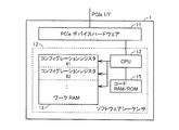
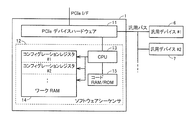
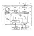
- FIG. 2 is a block diagram illustrating a configuration example of the semiconductor device according to the first embodiment.
- the semiconductor device 1 includes a PCIe device hardware 11 and a software sequencer 12.
- the software sequencer 12 includes a CPU 13, a work RAM (Random Access Memory) 14, and a code RAM / ROM (Read Only Memory) 15.
- the semiconductor device 1 communicates with a PCIe host via a PCIe I / F.
- the PCIe device hardware 11 is connected to the PCIe I / F and mainly controls the physical layer and the data link layer.
- the CPU 13 mainly controls the transaction layer by executing a program stored in the code RAM / ROM 15.
- the work RAM 14 stores a configuration register, details of which will be described later.
- the transaction layer mainly generates and decrypts transaction layer packets (TLPs).
- TLP includes commands such as read and write, addresses, data, and the like.
- the transaction layer also performs flow control with the connection partner.
- PCIe flow control is performed on a credit basis.
- the credit base is a method of notifying the partner of the size of a buffer that can be received in advance and notifying the buffer whenever there is a free space.
- the transmission side adds up the size of the packet received by itself, and subtracts the amount when the buffer is notified from the transmission partner. As a result, the packet can be transferred without exceeding the buffer size of the transmission partner.
- the transaction layer supports three address spaces: memory space, I / O space, and configuration space.
- PCIe PCIe
- PCI bus PCIe bus
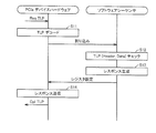
- FIG. 3 is a flowchart for explaining operations of the PCIe device hardware 11 and the software sequencer 12 when the PCIe device hardware 11 receives a request packet.
- the PCIe device hardware 11 receives a request packet (Req TLP) from the PCIe host via the PCIe I / F, it determines the request by decoding the TLP and responds to the request.
- An interrupt request is output to the CPU 13 of the software sequencer 12 (S11).
- the request packet includes a memory request that is a read / write request to the memory, an I / O request that is a read / write request to I / O, a configuration request that is a read / write request to the configuration space, and the like.
- the CPU 13 in the software sequencer 12 Upon receiving an interrupt request from the PCIe device hardware 11, the CPU 13 in the software sequencer 12 checks the TLP header and data (S12), generates a response to the request packet, and sets that the response has been generated in the control register. (S13). At this time, the value of the configuration register stored in the work RAM 14 is referred to as appropriate.
- the PCIe device hardware 11 When the PCIe device hardware 11 receives the response generated from the software sequencer 12, the PCIe device hardware 11 transmits a response (Cpl TLP: completion) via the PCIe I / F (S14). At this time, in the case of reading, data is also included in the response.
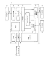
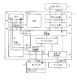
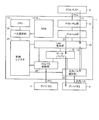
- FIG. 4 is a block diagram for explaining a more detailed configuration of the semiconductor device according to the first embodiment.
- the semiconductor device 1 includes a CPU 13, RAMs 14 and 15, a PCIe-Phys unit 21, a PCIe-Link unit 22, a link control unit 23, a control register 24, a data buffer 25, a PCI bus control unit 26, A general-purpose bus control unit 27 and a bus selection unit 28 are included.
- the PCIe-Phy unit 21 is connected to the PCIe host 2 via the PCIe I / F and has a function of the physical layer of PCIe.
- the PCIe-Link unit 22 has a function of a PCIe data link layer.
- the link control unit 23 decodes the received TLP (request packet) output from the PCIe-Link unit 22, determines what kind of request it is, and outputs an interrupt request to the CPU 13. Further, the link control unit 23 transmits a response (completion) corresponding to the request packet to the PCIe host 2 via the PCIe-Link unit 22 and the PCIe-Phys unit 21.
- the control register 24 is a group of registers provided for controlling the semiconductor device 1 itself, and is distinguished from the configuration register.
- the data buffer 25 transmits data to the device A (3) or the device B (4) via the PCI bus or general-purpose bus, and from the device A (3) or the device B (4) via the PCI bus or general-purpose bus. Store received data temporarily.
- the PCI bus control unit 26 transmits / receives data to / from the device A (3) when the request packet is a memory read or a memory write to the device A (3) connected to the PCI bus.
- the general-purpose bus control unit 27 transmits / receives data to / from the device B (4) when the request packet is a memory read or memory write to the device B (4) connected to the general-purpose bus.
- the bus selection unit 28 is connected to the downloader 5, the CPU 13, the RAMs 14 and 15, and the control register 24, and switches the bus. For example, when the downloader 5 downloads the program executed by the CPU 13 to the RAM 15, the bus selection unit 28 switches the bus so that the processing code output from the downloader 5 is written to the RAM 15.
- the bus selection unit 28 switches the bus so that the CPU 13 can fetch the processing code stored in the RAM 15.
- the bus selection unit 28 switches the bus so that the CPU 13 can read / write data from / to the control register 24.
- FIG. 5 to 6 are diagrams showing examples of the topology realized by the semiconductor device according to the first embodiment.
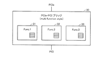
- FIG. 5 is a diagram illustrating an example in which the configuration of the PCIe-PCI bridge is realized by the semiconductor device 1 according to the first embodiment.
- This PCIe-PCI bridge 30 has three device functions (Func. 1 to Func. 3) 31 to 33, and three configuration registers corresponding to each of them are stored in the RAM 14 shown in FIGS. Be placed.
- the functions of the device functions 31 to 33 are realized by the CPU 13 executing the program stored in the RAM 15.
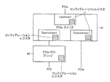
- FIG. 6 is a diagram illustrating an example in which the configuration of the PCIe switch and the PCIe-PCI bridge is realized by the semiconductor device 1 according to the first embodiment.
- the PCIe switch 41 has an upstream port (Upstream) and two downstream ports (Downstream), and three configuration registers corresponding to the upstream port (Upstream) are arranged in the RAM 14 shown in FIGS. 2 and 4.
- the PCIe-PCI bridge 42 has one configuration register and is arranged in the RAM 14 shown in FIGS.
- the PCIe host 2 searches the PCIe topology by reading the configuration register corresponding to each device function when the system is started. When the device function number in each device function hits the device function number of the configuration register defined in the RAM 14, the Link control unit 23 returns a completion meaning that the device function exists in accordance with an instruction from the CPU 13. Then, the PCIe host 2 is made to recognize the device function.
- FIG. 7 is a diagram for explaining the read operation of the configuration register when the topology shown in FIGS. 5 and 6 is realized by the semiconductor device 1 in the first embodiment shown in FIG.
- the link control unit 23 when the link control unit 23 receives a request packet from the PCIe host 2 via the PCIe-Phys unit 21 and the PCIe-Link unit 22 ((1) in FIG. 7), it decodes the TPL. When detecting that the TPL is a configuration read, the link control unit 23 notifies the CPU 13 that the configuration read has been received ((2) in FIG. 7).
- This notification may be made to output an interrupt request to the CPU 13 as described above, or the fact that the link control unit 23 has received the configuration read is written in the control register 24 and the CPU 13 polls it. You may make it notify by.
- the CPU 13 Upon receiving the notification from the link control unit 23, the CPU 13 reads the contents of the corresponding configuration register from the RAM 14 ((3) in FIG. 7) and sets the data in the link control unit 23 ((4) in FIG. 7). ). Then, the link control unit 23 transmits the completion to the PCIe host 2 via the PCIe-Link unit 22 and the PCIe-Phy unit 21 and transmits the contents of the configuration register.
- the configuration registers corresponding to the device functions 31 to 33 are stored in the RAM 14.
- the CPU 13 reads the contents of the configuration register corresponding to the device function requested from the PCIe host 2 from the RAM 14 and sets it in the link control unit 23.
- the RAM 14 has three configuration registers including the upstream port (Upstream) and the two downstream ports (Downstream) of the PCIe switch 41. And one configuration register of the PCIe-PCI bridge 42 is stored.
- the CPU 13 reads the contents of the configuration register corresponding to the device requested from the PCIe host 2 from the RAM 14 and sets the contents in the link control unit 23.
- FIG. 8 illustrates a read operation of the configuration register of the device connected to the PCI bus when the topology shown in FIGS. 5 and 6 is realized by the semiconductor device 1 in the first embodiment shown in FIG. FIG.
- the link control unit 23 when the link control unit 23 receives a request packet from the PCIe host 2 via the PCIe-Phy unit 21 and the PCIe-Link unit 22 ((1) in FIG. 8), it decodes the TPL. Then, when detecting that the TPL is the configuration read of the device A (3), the Link control unit 23 notifies the CPU 13 that the configuration read has been received ((2) in FIG. 8).
- the CPU 13 When the CPU 13 receives the notification from the link control unit 23, it requests the PCI bus control unit 26 for a PCI configuration read cycle ((3) in FIG. 8). Then, the PCI bus control unit 26 issues a configuration read to the device A (3) ((4) in FIG. 8).
- the device A (3) Upon receiving a configuration read from the PCI bus control unit 26, the device A (3) transmits the contents of the configuration register to the PCI bus control unit 26. Then, the PCI bus control unit 26 notifies the CPU 13 of the read data received from the device A (3) ((5) in FIG. 8).
- the CPU 13 sets the contents of the configuration register received from the PCI bus control unit 26 in the Link control unit 23 ((6) in FIG. 8). Then, the link control unit 23 transmits the completion to the PCIe host 2 via the PCIe-Link unit 22 and the PCIe-Phy unit 21 and transmits the contents of the configuration register.
- FIG. 9 is a diagram for explaining the operation of the memory read of the device connected to the PCI bus when the topology shown in FIGS. 5 and 6 is realized by the semiconductor device 1 in the first embodiment shown in FIG. It is.
- the link control unit 23 when the link control unit 23 receives a request packet from the PCIe host 2 via the PCIe-Phy unit 21 and the PCIe-Link unit 22 ((1) in FIG. 9), it decodes the TPL. Then, when detecting that the TPL is a memory read of the device A (3), the Link control unit 23 notifies the PCI bus control unit 26 that the memory read has been received ((2) in FIG. 9). ).
- the PCI bus control unit 26 Upon receiving the notification from the Link control unit 23, the PCI bus control unit 26 issues a memory read to the device A (3) ((3) in FIG. 9). When the PCI bus control unit 26 receives the read data from the device A (3), it sequentially stores it in the data buffer 25 ((4) in FIG. 9).
- the PCI bus control unit 26 completes the reception of the read data
- the PCI bus control unit 26 notifies the link control unit 23 of the completion of the read data ((5) in FIG. 9).
- the link control unit 23 receives a notification from the PCI bus control unit 26
- the completion data is transmitted to the PCIe host 2 via the PCIe-Link unit 22 and the PCIe-Phys unit 21 and read data stored in the data buffer 25. Are sent sequentially.
- memory write to the device A (3) is performed by the same operation as that shown in FIG. 16 described later, except that data is written to the device A (3) via the PCI bus control unit 26.
- the semiconductor device stores the configuration register of the PCIe device constituting the PCIe topology in the RAM 14 and the configuration stored in the RAM 14 when a request is received from the PCIe host 2.
- the response is transmitted to the PCIe host 2 with reference to the register.
- a topology in which a plurality of PCIe devices such as a PCIe-PCI bridge, a PCIe switch, and an endpoint are arbitrarily combined is configured by the semiconductor device in the present embodiment, a physical layer, a data link layer, etc. between the PCIe devices
- the hardware for controlling can be reduced. Therefore, it is possible to reduce the board area and component cost, and to reduce the number of gates and the package size.
- the memory read operation of the device connected to the PCI bus is performed without using the CPU 13.
- the memory transfer time is shortened, but the memory transfer is not limited to this method, and the memory transfer may be performed via the CPU 13.
- the semiconductor device stores a configuration register corresponding to a general-purpose device connected to a general-purpose bus in the RAM 14, and uses the configuration register to make the general-purpose device pseudo PCIe topology. It is controlled as a connected device.
- the configuration of the semiconductor device in the second embodiment is the same as the configuration of the semiconductor device in the first embodiment shown in FIG. Therefore, detailed description of overlapping configurations and functions will not be repeated.
- FIG. 10 is a block diagram illustrating a configuration example of the semiconductor device according to the second embodiment.
- the PCIe device hardware 11 is connected to the general-purpose devices 6 and 7 via the general-purpose bus. Therefore, detailed description of overlapping configurations and functions will not be repeated.
- the general-purpose bus refers to a bus other than the above-described PCIe bus and PCI bus.
- FIG. 11 to FIG. 14 are diagrams showing examples of the topology realized by the semiconductor device according to the second embodiment.
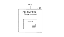
- FIG. 11 is a diagram illustrating an example in which the configuration of the PCIe end point (general-purpose device) 51 is realized by the semiconductor device 1 according to the second embodiment.
- This endpoint has only one device function (Func. 1), and a corresponding configuration register is arranged in the RAM 14 shown in FIGS.
- FIG. 12 is a diagram illustrating an example in which the configuration of the PCIe end point (general-purpose device) 60 is realized by the semiconductor device 1 according to the second embodiment.
- This end point has three device functions (Func. 1 to Func. 3) 61 to 63, and configuration registers corresponding to the three device functions 61 to 63 are shown in FIGS.
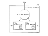
- FIG. 13 is a diagram illustrating an example of realizing the configuration of the topology 70 having the PCIe switch 71 and the two PCIe end points 72 and 73 by the semiconductor device 1 according to the second embodiment.
- Configuration switches corresponding to the PCIe switch 71 and the two PCIe endpoints 72 and 73 are arranged in the RAM 14 shown in FIGS. 2 and 4. In this case, the total number of configuration registers is 5.
- FIG. 14 is a diagram illustrating an example of realizing the configuration of the topology 80 having three PCIe switches and five PCIe end points by the semiconductor device 1 according to the second embodiment.
- Configuration registers corresponding to the three PCIe switches 1 to 3 (81 to 83) and the five PCIe end points 84 to 88 are arranged in the RAM 14 shown in FIGS. In this case, the total number of configuration registers is 14.
- FIG. 15 is a diagram for explaining the write operation of the configuration register when the topologies shown in FIGS. 11 to 14 are realized by the semiconductor device 1 according to the second embodiment.
- the link control unit 23 when the link control unit 23 receives a request packet from the PCIe host 2 via the PCIe-Phy unit 21 and the PCIe-Link unit 22 ((1) in FIG. 15), it decodes the TPL. Then, when detecting that the TPL is a configuration light, the link control unit 23 notifies the CPU 13 that the configuration light has been received ((2) in FIG. 15). At this time, the link control unit 23 also receives write data from the PCIe host 2 and transfers it to the CPU 13.
- the CPU 13 Upon receiving the notification from the link control unit 23, the CPU 13 writes the contents of the configuration register received from the link control unit 23 into the RAM 14 ((3) in FIG. 15), and the CPU 13 loads the general-purpose bus control unit 27 as necessary.
- the change of the operation setting is notified to the device B (4) via (4) of FIG.
- the CPU 13 sets the response status in the link control unit 23 ((5) in FIG. 15). Then, the link control unit 23 transmits a completion to the PCIe host 2 via the PCIe-Link unit 22 and the PCIe-Phy unit 21 ((6) in FIG. 15).
- FIG. 16 is a diagram for explaining a memory write operation of a device connected to the general-purpose bus when the topologies shown in FIGS. 11 to 14 are realized by the semiconductor device 1 according to the second embodiment.
- the link control unit 23 when the link control unit 23 receives a request packet from the PCIe host 2 via the PCIe-Phys unit 21 and the PCIe-Link unit 22 ((1) in FIG. 16), it decodes the TPL. Then, when detecting that the TPL is a memory write of the device B (4), the Link control unit 23 stores the write data received from the PCIe host 2 in the data buffer 25 ((2) in FIG. 16).
- the Link control unit 23 notifies the general-purpose bus control unit 27 that the memory write has been received ((3) in FIG. 16).
- the general-purpose bus control unit 27 issues a memory write to the device B (4), and sequentially transmits the write data stored in the data buffer 25 to the device B (4) ((4) in FIG. 16). .
- memory read from the device B (4) connected to the general-purpose bus is performed by the same operation as in FIG. 9 described above, and only data is read from the device B (4) via the general-purpose bus control unit 27. Is different.
- the semiconductor device stores the configuration register of the general-purpose device connected to the general-purpose bus in the RAM 14 and the contents of the configuration register with respect to the configuration read from the PCIe host 2. return it. Therefore, in addition to the effects described in the first embodiment, the semiconductor device in this embodiment can pseudo-connect a general-purpose register to the PCIe topology.
Landscapes
- Engineering & Computer Science (AREA)
- Theoretical Computer Science (AREA)
- General Engineering & Computer Science (AREA)
- Physics & Mathematics (AREA)
- General Physics & Mathematics (AREA)
- Computer Hardware Design (AREA)
- Bus Control (AREA)
- Information Transfer Systems (AREA)
Abstract
Description
図2は、第1の実施の形態における半導体装置の構成例を示すブロック図である。この半導体装置1は、PCIeデバイスハードウェア11と、ソフトウェアシーケンサ12とを含む。また、ソフトウェアシーケンサ12は、CPU13と、ワークRAM(Random Access Memory)14と、コードRAM/ROM(Read Only Memory)15とを含む。半導体装置1は、PCIe I/Fを介して、PCIeホストとの通信を行なう。
第2の実施の形態における半導体装置は、汎用バスに接続される汎用デバイスに対応するコンフィグレーションレジスタをRAM14に記憶し、そのコンフィグレーションレジスタを用いることによって、汎用デバイスを擬似的にPCIeのトポロジに接続されたデバイスとして制御するものである。なお、第2の実施の形態における半導体装置の構成は、図4に示す第1の実施の形態における半導体装置の構成と同様である。したがって、重複する構成および機能の詳細な説明は繰り返さない。
汎用デバイス、11 PCIeデバイスハードウェア、12 ソフトウェアシーケンサ、13 CPU、14 ワークRAM、15 コードRAM/ROM、21 PCIe-Phy部、22 PCIe-Link部、23 Link制御部、24 制御レジスタ、25 データバッファ、26 PCIバス制御部、27 汎用バス制御部、28 バス選択部。
Claims (8)
- シリアルインタフェースバスのトポロジを構成するデバイスを実現する半導体装置であって、
プロセッサと、
前記プロセッサによって参照されるデータを記憶する記憶部と、
前記シリアルインタフェースバスの物理レイヤおよびデータリンクレイヤを制御するシリアルインタフェースバス制御部とを含み、
前記記憶部は、前記デバイスのファンクション情報を定義するコンフィグレーションレジスタを記憶し、
前記シリアルインタフェースバス制御部は、ホストから受信したリクエストをデコードし、デコード結果を前記プロセッサに出力し、
前記プロセッサは、前記シリアルインタフェースバス制御部から受けたデコード結果に応じて対応するコンフィグレーションレジスタを前記記憶部から読み出し、前記リクエストに対するレスポンスを生成して前記シリアルインタフェースバス制御部に送信させる、半導体装置。 - 前記シリアルインタフェースバスは、PCIeバスである、請求項1記載の半導体装置。
- 前記プロセッサは、前記記憶部に記憶されるコンフィグレーションレジスタの総数および各コンフィグレーションレジスタごとの機能を変更することで、前記半導体装置によって実現されるデバイスを変更する、請求項1または2記載の半導体装置。
- 前記半導体装置はさらに、PCIバスに接続されるデバイスとの間のデータの送受信を制御するPCIバス制御部を含み、
前記シリアルインタフェースバス制御部によるデコード結果が前記PCIバスに接続されるデバイスの制御に関するリクエストである場合、前記PCIバス制御部は、前記PCIバスに接続されるデバイスとの間でデータの送受信を行なうことにより、ブリッジの機能を実現する、請求項1または2に記載の半導体装置。 - 前記記憶部は、上流側ポートおよび下流側ポートのそれぞれのコンフィグレーションレジスタを記憶し、
前記シリアルインタフェースバス制御部によるデコード結果が前記上流側ポートまたは下流側ポートのコンフィグレーションリードの場合、前記プロセッサは対応するコンフィグレーションレジスタを前記記憶部から読み出して前記シリアルインタフェースバス制御部に送信させることにより、前記ブリッジおよびスイッチの機能を実現する、請求項4記載の半導体装置。 - 前記半導体装置はさらに、汎用バスに接続される汎用デバイスとの間のデータの送受信を制御する汎用バス制御部を含み、
前記記憶部は、前記汎用デバイスに対応するコンフィグレーションレジスタを記憶し、
前記シリアルインタフェースバス制御部によるデコード結果が前記汎用デバイスのコンフィグレーションリードの場合、前記プロセッサは前記汎用デバイスに対応するコンフィグレーションレジスタを前記記憶部から読み出して前記シリアルインタフェースバス制御部に送信させ、前記シリアルインタフェースバス制御部によるデコード結果が前記汎用デバイスの制御に関するリクエストである場合、前記汎用バス制御部は、前記汎用デバイスとの間でデータの送受信を行なうことにより、前記汎用デバイスを擬似的に前記シリアルインタフェースバスのトポロジに接続されたデバイスとして制御する、請求項1または2に記載の半導体装置。 - 前記シリアルインタフェースバス制御部は、前記ホストから受信したリクエストのデコード結果に対応する割込み要求を前記プロセッサに出力し、
前記プロセッサは、前記シリアルインタフェースバス制御部から受けた割込み要求に応じて対応するコンフィグレーションレジスタを参照する、請求項1記載の半導体装置。 - 前記シリアルインタフェースバス制御部は、前記ホストから受信したリクエストのデコード結果をレジスタに書き込み、
前記プロセッサは、前記レジスタに書き込まれたデコード結果をポーリングすることによって、前記シリアルインタフェースバス制御部から受けたリクエストを判断し、対応するコンフィグレーションレジスタを参照する、請求項1記載の半導体装置。
Priority Applications (2)
| Application Number | Priority Date | Filing Date | Title |
|---|---|---|---|
| US13/984,428 US20130326097A1 (en) | 2011-03-17 | 2012-02-17 | Semiconductor device |
| JP2013504621A JPWO2012124431A1 (ja) | 2011-03-17 | 2012-02-17 | 半導体装置 |
Applications Claiming Priority (2)
| Application Number | Priority Date | Filing Date | Title |
|---|---|---|---|
| JP2011-059318 | 2011-03-17 | ||
| JP2011059318 | 2011-03-17 |
Publications (1)
| Publication Number | Publication Date |
|---|---|
| WO2012124431A1 true WO2012124431A1 (ja) | 2012-09-20 |
Family
ID=46830508
Family Applications (1)
| Application Number | Title | Priority Date | Filing Date |
|---|---|---|---|
| PCT/JP2012/053761 Ceased WO2012124431A1 (ja) | 2011-03-17 | 2012-02-17 | 半導体装置 |
Country Status (3)
| Country | Link |
|---|---|
| US (1) | US20130326097A1 (ja) |
| JP (1) | JPWO2012124431A1 (ja) |
| WO (1) | WO2012124431A1 (ja) |
Cited By (4)
| Publication number | Priority date | Publication date | Assignee | Title |
|---|---|---|---|---|
| US20140289444A1 (en) * | 2013-03-19 | 2014-09-25 | Fujitsu Limited | Information processing apparatus and method of controlling |
| KR20160106486A (ko) * | 2015-03-02 | 2016-09-12 | 삼성전자주식회사 | 불휘발성 메모리 모듈 어레이 시스템 |
| CN107992438A (zh) * | 2017-11-24 | 2018-05-04 | 郑州云海信息技术有限公司 | 一种服务器及在服务器内灵活配置PCIe拓扑的方法 |
| US20220086101A1 (en) * | 2020-09-17 | 2022-03-17 | Honda Motor Co., Ltd. | Communication control apparatus, communication system, communication control method, and storage medium |
Citations (2)
| Publication number | Priority date | Publication date | Assignee | Title |
|---|---|---|---|---|
| JP2006195870A (ja) * | 2005-01-17 | 2006-07-27 | Ricoh Co Ltd | データ転送システム及び電子機器 |
| JP2009169842A (ja) * | 2008-01-18 | 2009-07-30 | Hitachi Ltd | 複合型計算機システムの管理方法及び複合型計算機システム |
Family Cites Families (5)
| Publication number | Priority date | Publication date | Assignee | Title |
|---|---|---|---|---|
| US6076160A (en) * | 1997-11-20 | 2000-06-13 | Advanced Micro Devices, Inc. | Hardware-based system for enabling data transfers between a CPU and chip set logic of a computer system on both edges of bus clock signal |
| JPH11238030A (ja) * | 1998-02-20 | 1999-08-31 | Mitsubishi Electric Corp | Pci−pciブリッジおよびそのための先入れ先出しメモリ |
| JPH11288400A (ja) * | 1998-04-03 | 1999-10-19 | Nec Shizuoka Ltd | Pciブリッジデバイス |
| JP2009037674A (ja) * | 2007-07-31 | 2009-02-19 | Ntn Corp | ハードディスクドライブの評価方法 |
| US8234458B2 (en) * | 2008-12-09 | 2012-07-31 | Nvidia Corporation | System and method for maintaining cache coherency across a serial interface bus using a snoop request and complete message |
-
2012
- 2012-02-17 US US13/984,428 patent/US20130326097A1/en not_active Abandoned
- 2012-02-17 WO PCT/JP2012/053761 patent/WO2012124431A1/ja not_active Ceased
- 2012-02-17 JP JP2013504621A patent/JPWO2012124431A1/ja active Pending
Patent Citations (2)
| Publication number | Priority date | Publication date | Assignee | Title |
|---|---|---|---|---|
| JP2006195870A (ja) * | 2005-01-17 | 2006-07-27 | Ricoh Co Ltd | データ転送システム及び電子機器 |
| JP2009169842A (ja) * | 2008-01-18 | 2009-07-30 | Hitachi Ltd | 複合型計算機システムの管理方法及び複合型計算機システム |
Cited By (7)
| Publication number | Priority date | Publication date | Assignee | Title |
|---|---|---|---|---|
| US20140289444A1 (en) * | 2013-03-19 | 2014-09-25 | Fujitsu Limited | Information processing apparatus and method of controlling |
| JP2014182604A (ja) * | 2013-03-19 | 2014-09-29 | Fujitsu Ltd | 情報処理装置及び制御方法 |
| KR20160106486A (ko) * | 2015-03-02 | 2016-09-12 | 삼성전자주식회사 | 불휘발성 메모리 모듈 어레이 시스템 |
| KR102262807B1 (ko) | 2015-03-02 | 2021-06-09 | 삼성전자주식회사 | 불휘발성 메모리 모듈 어레이 시스템 |
| CN107992438A (zh) * | 2017-11-24 | 2018-05-04 | 郑州云海信息技术有限公司 | 一种服务器及在服务器内灵活配置PCIe拓扑的方法 |
| US20220086101A1 (en) * | 2020-09-17 | 2022-03-17 | Honda Motor Co., Ltd. | Communication control apparatus, communication system, communication control method, and storage medium |
| US12231348B2 (en) * | 2020-09-17 | 2025-02-18 | Honda Motor Co., Ltd. | Communication control apparatus, communication system, communication control method, and storage medium for determining whether to permit data transmission |
Also Published As
| Publication number | Publication date |
|---|---|
| US20130326097A1 (en) | 2013-12-05 |
| JPWO2012124431A1 (ja) | 2014-07-17 |
Similar Documents
| Publication | Publication Date | Title |
|---|---|---|
| CN113434446B (zh) | 灵活总线协议协商和启用序列 | |
| CN102511039B (zh) | 将不可预取存储单元映射到存储器映射输入/输出空间中 | |
| US10210120B2 (en) | Method, apparatus and system to implement secondary bus functionality via a reconfigurable virtual switch | |
| CN112631959B (zh) | 用于一致性消息的高带宽链路层 | |
| JP4589384B2 (ja) | 高速メモリモジュール | |
| US20150347345A1 (en) | Gen3 pci-express riser | |
| JP7391154B2 (ja) | デイジーチェーンspi集積回路およびその動作方法 | |
| JP5824488B2 (ja) | トランザクション属性を修正するためのメモリ領域オーダリング要求に関するコンプリータ知識の使用 | |
| EP3213220B1 (en) | Methods and circuits for deadlock avoidance | |
| JPH11238030A (ja) | Pci−pciブリッジおよびそのための先入れ先出しメモリ | |
| CN108304334B (zh) | 应用处理器和包括中断控制器的集成电路 | |
| CN110659221A (zh) | 主机管理的相干设备存储器 | |
| JP2008090375A (ja) | 割込み制御システム、およびこれを利用した記憶制御システム | |
| US20160380747A1 (en) | Flexible interconnect architecture | |
| US20080250186A1 (en) | Bus connecting device for connecting host with external device | |
| WO2012124431A1 (ja) | 半導体装置 | |
| US7096290B2 (en) | On-chip high speed data interface | |
| US9563586B2 (en) | Shims for processor interface | |
| US8996772B1 (en) | Host communication device and method with data transfer scheduler | |
| CN105068962A (zh) | I2c控制器访问方法及系统 | |
| KR100684553B1 (ko) | 듀얼 포트 메모리와 결합되는 마이크로 프로세서 | |
| TW201916644A (zh) | 匯流排系統 | |
| CN110399322B (zh) | 一种数据传输方法及乒乓dma架构 | |
| CN101676894B (zh) | 面向集中地址译码的非pci片上总线的pci虚拟化装置及方法 | |
| TWI526842B (zh) | 應用於x86系統之訊號寫入之控制與切換模組 |
Legal Events
| Date | Code | Title | Description |
|---|---|---|---|
| 121 | Ep: the epo has been informed by wipo that ep was designated in this application |
Ref document number: 12758181 Country of ref document: EP Kind code of ref document: A1 |
|
| ENP | Entry into the national phase |
Ref document number: 2013504621 Country of ref document: JP Kind code of ref document: A |
|
| WWE | Wipo information: entry into national phase |
Ref document number: 13984428 Country of ref document: US |
|
| NENP | Non-entry into the national phase |
Ref country code: DE |
|
| 122 | Ep: pct application non-entry in european phase |
Ref document number: 12758181 Country of ref document: EP Kind code of ref document: A1 |