WO2012121293A1 - 基板レイアウト評価装置および評価方法、基板レイアウト設計システム - Google Patents
基板レイアウト評価装置および評価方法、基板レイアウト設計システム Download PDFInfo
- Publication number
- WO2012121293A1 WO2012121293A1 PCT/JP2012/055833 JP2012055833W WO2012121293A1 WO 2012121293 A1 WO2012121293 A1 WO 2012121293A1 JP 2012055833 W JP2012055833 W JP 2012055833W WO 2012121293 A1 WO2012121293 A1 WO 2012121293A1
- Authority
- WO
- WIPO (PCT)
- Prior art keywords
- wiring
- terminal
- terminals
- electrical net
- evaluation
- Prior art date
- Legal status (The legal status is an assumption and is not a legal conclusion. Google has not performed a legal analysis and makes no representation as to the accuracy of the status listed.)
- Ceased
Links
Images





Classifications
-
- G—PHYSICS
- G06—COMPUTING OR CALCULATING; COUNTING
- G06F—ELECTRIC DIGITAL DATA PROCESSING
- G06F30/00—Computer-aided design [CAD]
- G06F30/30—Circuit design
- G06F30/39—Circuit design at the physical level
- G06F30/398—Design verification or optimisation, e.g. using design rule check [DRC], layout versus schematics [LVS] or finite element methods [FEM]
Definitions
- the present invention relates to a printed circuit board layout evaluation apparatus and evaluation method. Moreover, it is related with the board
- the board layout design related to the high-speed signal wiring it is not sufficient to consider the signal wiring for connecting the terminals of the components to each other. For example, even if a resistor is inserted in series with the signal line, the high-speed signal propagates from one wiring to the other wiring through the resistor. In this specification, a wiring that is considered to propagate a signal through a component is referred to as an electrical net in this specification. In the board layout design of high-speed signal wiring, it is necessary to determine the board layout in consideration of the wiring length of the electrical net and the return current path of the electrical net.
- a CAD Computer Aided Design
- the layout data is data generated when a layout designer designs a board layout on a CAD system based on circuit diagram data.
- This evaluation function is provided as being attached to CAD or as being independent of CAD.
- the evaluation function evaluates whether the wiring length of the high-speed signal wiring is designed to be short in the layout of the printed circuit board defined by the layout data.
- the wiring length considers the electrical net as described above. For example, when a resistor is connected in series in the signal wiring, the path length of the wiring combining two high-speed signal wirings connected via the resistor is calculated and evaluated.
- the path length of the wiring from the calculation start point specified on a certain wiring (net) to the calculation end point specified on the same or different wiring There are known systems for calculating.
- “net” has a different meaning from “electrical net”.
- a simple “net” refers to an individual wiring that is electrically connected without a component.
- An electrical net is a set of nets, which are a plurality of wires that are considered to propagate signals through components and therefore should be considered to be electrically connected.
- the above-described wiring length calculation system records information on each electronic component in advance as a passage parameter.
- the passing parameter is passing terminal information that defines from which terminal to which terminal the wiring path is considered to pass when the electronic component mounted on the printed wiring board searches for the wiring path.
- searching for the wiring route it is determined whether or not the wiring route is allowed to pass from one terminal of the predetermined electronic component to another terminal based on the passage parameter.
- the wiring path length can be calculated for wiring paths between predetermined points existing in different nets. And it is test
- the wiring length calculation system determines that there is a wiring path from one point to another point, and calculates the path length of the wiring path.
- the wiring length can be calculated for different nets on the wiring board, but it is necessary to set the passing parameters for all the components connected to the net. Effort is required to preset the passing parameters.
- the wiring length can be calculated using the library. That is, it is not necessary to set parameters every time the board layout design is performed.
- confirmation can be performed only in an environment where the library is applicable. That is, an environment where the library is not applicable, for example, a board designed by another CAD cannot be evaluated.
- the present invention has been made in consideration of the above-described circumstances, and searches for an electrical net without considering complicated pre-setting such as a passage parameter for a part, and considers the found electrical net.
- a substrate layout evaluation apparatus capable of evaluating a substrate layout is provided.
- substrate layout design system provided with the corresponding evaluation method and the said evaluation apparatus is provided.
- the present invention relates to a layout data reference unit that refers to layout data for printed circuit board wiring and components connected by the wiring, and an evaluation object that specifies a wiring to be evaluated among the wirings included in the layout data. If there are two-terminal parts in the designated part, the passive-part extracting part that extracts the passive parts connected to the wiring that has been evaluated, and the extracted passive parts, If there is a multi-terminal component having four or more terminals in the extracted passive component, and a two-terminal electrical net search unit that searches for a two-terminal electrical net that is a wiring connected to one of the wirings, the multi-terminal component A multi-terminal electrical network that searches for a multi-terminal electrical net that is a wiring that should be regarded as a signal propagating from one of the wirings to be evaluated A multi-terminal electrical net search unit based on an outer shape of the passive component, and a terminal component of the passive component, comprising: a Lunet search unit; and an evaluation processing unit that evaluates a board layout using the
- the terminal on the same side as the terminal connected to one of the wirings to be evaluated in (1) or the terminal at the opposite position on the opposite side is set as a propagation candidate terminal, and the wiring is connected to another component of the propagation candidate terminals. If there are a plurality of terminals connected in common, these terminals are regarded as a group of non-propagating terminals, and a group of non-propagating terminals including terminals connected to the wiring to be evaluated are excluded from the propagation candidate terminals.
- the wiring connected to the propagation terminal is the multi-terminal electrical net
- the evaluation processing unit includes the wiring to be evaluated and the two-terminal electrical net and / or the The wiring length of the electrical net as a set of terminal electrical nets, whether or not guard wiring is arranged on both sides of the electrical net, and / or whether or not a return current path for signals related to the electrical net is arranged
- a substrate layout evaluation apparatus that evaluates the substrate layout using as an index is provided. In other words, when the two-terminal electrical net search unit has two terminals among the extracted passive components, the signal propagates from the wiring to be evaluated via the two-terminal passive components. This is to search for wiring to be considered.
- the multi-terminal electrical net search unit when the extracted passive component includes four or more terminals, the signal propagates from the wiring to be evaluated through the passive component having four or more terminals. This is to search for wiring to be considered. Specifically, the two-terminal electrical net search unit considers that the signal propagates from the wiring designated as the evaluation target to another wiring connected to a terminal different from the terminal connected to the evaluation target wiring. Add wiring to the evaluation target. When there are a plurality of terminals that are connected to the same component other than the passive component through wiring among the terminals of the passive component, the multi-terminal electrical net search unit sets the terminals as non-propagating terminals of the same set. Classify.
- a terminal arranged on the same side as the target terminal connected to the wiring to be evaluated and a terminal at a position opposite to the target terminal are set as propagation candidate terminals, Of the propagation candidate terminals, terminals that are not non-propagation terminals in the same set as the target terminal are defined as propagation terminals.
- the wiring connected to a propagation terminal is added to evaluation object.
- the evaluation processing unit defines a set of wirings specified by the evaluation target specifying unit and wirings added to the evaluation target by the two-terminal electrical net searching unit wiring and / or the multi-terminal electrical net searching unit as an electrical net. To do.
- the present invention relates to a step in which a computer refers to layout data for printed circuit board wiring and components connected by the wiring, and specifies wiring to be evaluated based on the layout information. Or receiving a designation by a user of a wiring to be evaluated from among the wirings included in the layout data, extracting a passive component connected to the wiring to be evaluated, and the extracted passive If there are two-terminal components in the component, a two-terminal electrical net search step for searching for a two-terminal electrical net that is a wiring connected to one of the wirings to be evaluated through the two-terminal passive component is extracted, If there is a multi-terminal component with 4 or more terminals among the passive components, the evaluation is made through the multi-terminal component.
- the step of searching for the multi-terminal electrical net is based on the outer shape of the passive component, and the terminal on the same side as the terminal connected to one of the wirings to be evaluated among the terminals of the passive component or the opposite side. If there are a plurality of terminals that are commonly connected via wiring to another one of the propagation candidate terminals, the terminal at the position is set as a propagation candidate terminal.
- a group of non-propagating terminals including a terminal connected to the target wiring is removed from the propagation candidate terminals as a propagation terminal, and the wiring connected to the propagation terminal
- the multi-terminal electrical net is used, and the evaluation step includes the wiring to be evaluated and the wiring length of the electrical net as a set of the two-terminal electrical net and / or the multi-terminal electrical net, and guard wiring is arranged on both sides of the electrical net.
- the two-terminal electrical net search step when the extracted passive component has two terminals, the signal propagates from the wiring to be evaluated via the two-terminal passive component. This is a step of searching for a wiring to be regarded.
- the multi-terminal electrical net search step when there are four or more extracted passive components, the signal propagates from the wiring to be evaluated through the passive components having four or more terminals. This is a step of searching for a wiring to be regarded.
- the two-terminal electrical net search step assumes that the signal is propagated from the wiring designated as the evaluation target to another wiring connected to a terminal different from the terminal connected to the evaluation target wiring. Add wiring to the evaluation target.
- the multi-terminal electrical net search step when there are a plurality of terminals connected to the same component other than the passive component through wiring among the terminals of the passive component, those terminals are set as non-propagating terminals of the same set. Classify. Further, based on the outer shape of the passive component, a terminal arranged on the same side as the target terminal connected to the wiring to be evaluated and a terminal at a position opposite to the target terminal are set as propagation candidate terminals, Of the propagation candidate terminals, terminals that are not non-propagation terminals in the same set as the target terminal are defined as propagation terminals. And the wiring connected to a propagation terminal is added to evaluation object.
- an electrical net is a set of wirings specified by the evaluation target specifying unit and wirings added to the evaluation target by the two-terminal electrical net searching unit wiring and / or the multi-terminal electrical net searching unit. .
- the present invention further includes the board layout evaluation apparatus, an input unit that receives an instruction from a user regarding board layout design, a layout generation unit that generates layout data based on the input instruction, and stores the generated layout data.
- a board layout design system comprising: a storage unit that performs a layout represented by the layout data; and an output unit that outputs an evaluation of the layout by the board layout evaluation apparatus.
- the two-terminal electrical net search unit considers that a signal is propagated from the evaluation target wiring to a wiring connected to one of the evaluation target wirings via a two-terminal component.
- the multi-terminal electrical net search unit is a terminal on the same side as the terminal connected to one of the wirings to be evaluated among the terminals of the passive component, or the opposite position on the opposite side. If there are a plurality of terminals that are commonly connected to another part of the propagation candidate terminals via wiring, the terminals are regarded as a group of non-propagation terminals and are evaluated.
- a group of non-propagating terminals including the terminals connected to the wirings are removed from the propagation candidate terminals to be the propagation terminals, and the wirings connected to the propagation terminals are added to the evaluation target, so that they pass through the parts. Even without complicated preset as parameters to search the electrical net which signals propagate from the evaluation of the target wiring, evaluation board layout in consideration of the found electrical net can be performed.
- the evaluation method and the board layout design system according to the present invention have the same effects.
- the board layout evaluation apparatus can be configured by being incorporated as a part of a CAD system used for board layout design.
- the printed circuit board is a board for realizing an electronic circuit having a predetermined function by electrically connecting components mounted on the board by wiring with a single layer or a multilayer wiring layer.
- Any substrate material or shape may be used as long as it is a target for substrate layout design by CAD. Therefore, it is not limited to a flat substrate, and includes a flexible film that can withstand bending. Typical examples thereof include, but are not limited to, a personal computer and a motherboard of a portable information terminal.
- the wiring is a conductor that is in the wiring layer formed on the surface of the substrate or inside the substrate and electrically connects a certain point to another point. Although typically linear, the ground wiring and the power supply wiring may be mounted as a “surface” region having a wide width.
- the component is an electronic component that constitutes a circuit. Components are roughly divided into active components and passive components.
- the active component is a component including a function of converting energy other than a signal into signal energy and amplifying it. Examples of passive components include resistors, capacitors, inductors, common mode choke coils, ferrite beads, and connectors.
- examples of active components include ICs (integrated circuits), transistors, and diodes. Each component has a terminal for connecting to the wiring on the substrate. Usually, the number of terminals of the component is two or more.
- the layout is stored in the storage unit as layout data.
- the layout data is usually generated by CAD for printed circuit board design.
- the layout data includes information such as the position, path, shape, width (wiring thickness) of the wiring to be arranged on the substrate. Furthermore, the information includes information such as the position and shape of the component to be arranged on the substrate, the type of passive component or active component, the arrangement and number of terminals.
- the storage unit is a storage device that stores layout data created by the layout generation unit. Specific examples thereof include a hard disk drive device and a flash memory (which may be arrayed as a solid state drive).
- the function of the evaluation target designating unit may be realized by a keyboard or mouse input interface circuit used for designating the evaluation target wiring and a processing program that causes the CPU to control the circuit.
- the CPU autonomously specifies the evaluation target based on the layout data
- the function of the evaluation target specifying unit is realized by a processing program executed by the CPU. Both aspects may be included.
- the functions of the passive component extraction unit, the two-terminal electrical net search unit, the multi-terminal electrical net search unit, and the evaluation processing unit are realized by the CPU performing processing while referring to the layout data. More specifically, the function is realized by a program that causes the CPU to execute a board layout evaluation process, a CPU that executes the program, and a storage device that stores the program so that the CPU can read the program.
- the CPU in this specification may be a single CPU, or a mode in which a plurality of CPUs cooperate to execute processing.
- One example is an aspect called so-called cloud computing and grid computing.
- the change is transmitted and the same potential change or current change occurs in the wiring connected to the other terminals. That is, the wiring connected to the other terminals also serves as a radiation source for unnecessary radiation noise.
- Active components drive signals themselves, while passive components passively transmit signals. In this invention, paying attention to the characteristics of such passive components, search for wiring through which unnecessary radiation noise propagates through the passive components, and suppress unnecessary radiation noise for an electrical net that is a set of wiring including these passive components. It is evaluated whether or not a layout in consideration is obtained.
- the external shape of the component is mainly a shape related to the external shape of the package and the arrangement of terminals on the package.
- Propagation candidate terminals are determined based on the idea that signals are not connected so that signals cross within the passive component.
- the non-propagating terminal is determined based on the idea that terminals connected to the same component outside are different signal lines.
- the width of the wiring, the attribute of the signal obtained from the net name, and the terminals on different sides of the package are usually connected straight in the case of 6 terminals or more. May be determined based on the premise that is connected.
- the evaluation processing unit performs the evaluation by using the wiring length of the searched electrical net, the presence or absence of the guard wiring, and / or the presence or absence of the return current path as an index.
- the wiring length takes into consideration a point related to the size of an antenna that radiates unnecessary radiation noise, that is, a radiation source.
- the guard wiring takes into account the noise shielding effect obtained by arranging constant potential wiring such as ground wiring near both sides of the electrical net.
- the return current path takes into consideration that the path length including not only the signal forward path but also the return path, that is, the path length of the current loop or the internal area of the current loop is related to the size of the radiation source.
- the signal return path is composed of ground wiring or power supply wiring.
- FIG. 1 is a configuration block diagram showing a substrate layout evaluation apparatus according to an embodiment of the present invention. It is explanatory drawing which shows an example of the board
- the wiring obtained by the search is a power supply or ground wiring
- the wiring may be excluded from the evaluation target. In this way, it is possible to exclude a power source and a ground wiring that are maintained at a constant voltage and do not become a generation source of unnecessary radiation noise from the electrical net, so that more accurate evaluation can be performed.
- the two-terminal electrical net search unit and the multi-terminal electrical net search unit both add the wiring obtained by the search to the evaluation target, and further search the added evaluation target wiring. Good. In this way, a wiring through which a signal further propagates through the passive component can be added to the evaluation object from the wiring obtained by the search, so that a more accurate evaluation can be performed.
- the multi-terminal electrical net search unit includes one or more non-propagating terminals in a certain passive component, but when there are a plurality of terminals that do not belong to any set, the multi-terminal electrical net search unit selects one terminal that does not belong to any set.
- a set of non-propagating terminals may be used.
- the multi-terminal electrical net searching unit may use three or more terminals arranged along the same side based on the component shape as a set of non-propagating terminals for six or more passive components. In this way, since the propagated terminal can be determined based on the shape of the passive component, the electrical net can be searched even when the propagated terminal cannot be determined from the connection relation of the wiring.
- the evaluation processing unit may compare the total wiring length of the electrical net with a predetermined threshold value and use it as an evaluation index. In this way, evaluation can be performed using the total wiring length of the electrical net that is a source of unwanted radiation noise.
- the evaluation processing unit may calculate a path length of a portion where the shield ground wiring is not arranged on both sides of the wiring to be evaluated, and may use it for the evaluation index. In this way, it is possible to consider the effect of suppressing unnecessary radiation noise by the shielding ground wiring, and therefore, more accurate evaluation can be performed.
- the printed circuit board is a multi-layer substrate
- the evaluation processing unit is a path of a portion where a ground region or a ground wiring corresponding to the wiring is not disposed in an adjacent layer of a wiring layer where the wiring to be evaluated exists.
- the length may be calculated and used as an evaluation index. In this way, it is possible to take into account the effect of suppressing unnecessary radiation noise by the ground wiring of the adjacent layer, so that more accurate evaluation can be performed.
- the evaluation processing unit has no ground wiring in the adjacent layer of the wiring layer where the wiring to be evaluated exists, or a portion having no ground area or ground wiring corresponding to the wiring even if there is an adjacent layer And the path length of the part where the ground wiring is not arranged on both sides of the wiring may be calculated and used as an evaluation index. In this way, it is possible to consider the effect of suppressing unnecessary radiation noise by the ground wiring on the adjacent layer or the ground wiring on both sides, so that more accurate evaluation can be performed.
- the various preferable aspects shown here can also be combined.
- FIG. 1 is a configuration block diagram showing a substrate layout evaluation apparatus according to an embodiment of the present invention.
- the board layout evaluation apparatus 4 of the present invention can be configured by being incorporated in a part of the board layout design system 15 used for board layout design.
- the board layout design system includes an input unit 1, a layout generation unit 2, a storage unit 3, a board layout evaluation device 4, and an output unit 13.
- the board layout evaluation apparatus 4 includes an evaluation object designating unit 5, a passive component extraction unit 6, a two-terminal electrical net search unit 7 (hereinafter, abbreviated as a two-terminal EN search unit), and a multi-terminal electrical net search unit 8. (Hereinafter abbreviated as a multi-terminal EN search unit), an evaluation processing unit 12 and a layout data reference unit 14 are provided.
- multi-terminal EN search unit 8 includes a non-propagation terminal classification unit 9, a propagation candidate terminal determination unit 10, and an electrical net search unit 11 (hereinafter abbreviated as an EN search unit).
- the input unit 1 receives input information in response to an operation in which a designer inputs information necessary for board layout design using a keyboard, a mouse, or the like.
- a specific mode is an interface circuit that takes an interface with hardware such as a keyboard and a mouse used for input operation, and software that controls the interface circuit.
- the evaluation object designating unit of the present invention includes the input unit 1 in the configuration, particularly when the user designates the wiring to be evaluated.
- the function of the layout generation unit 2 is realized by a program for causing the CPU to execute the process of board layout design, a CPU that executes the program, and a storage device that stores the processing program so that the CPU can read the program.
- a personal computer and a network server are mentioned as an example of the specific aspect of the hardware which provides the above-mentioned CPU and storage device.
- the layout generation unit 2 creates a board layout based on the input information and outputs layout data. When the evaluation apparatus of the present invention is independent from the CAD for board layout design, the layout generation unit 2 is not included in the configuration.
- the storage unit 3 is a storage device that stores the layout data created by the layout generation unit 2. Specific examples thereof include a hard disk drive device and a flash memory (which may be arrayed as a solid state drive). In addition to the layout data, the storage unit 3 may store a board layout design program to be executed by the CPU.
- the function of the board layout evaluation device 4 is realized by a program for causing the CPU to execute a board layout evaluation process, a CPU that executes the program, and a storage device that stores the program so that the CPU can read the program.
- the program may be stored in the storage unit 3, but may be stored in another storage device.
- the hardware that provides the CPU and the storage device described above may be the same as that of the layout generation unit 2, but may be different hardware. That is, a common computer or network server may be used for designing the board layout, but a different computer or network server may be used.
- the output unit 13 outputs the result evaluated by the board layout evaluation device 4. Specifically, the output unit 13 includes a display device for outputting an evaluation result, an interface circuit for operating the display device, and a processing program for causing the CPU to control the interface circuit. .
- the example shown in FIG. 1 uses hardware common to the board layout design and the board layout evaluation apparatus. However, regardless of whether the board layout design and the hardware used for the evaluation are common, the board layout evaluation device 4 performs the evaluation based on the layout data generated by the layout generation unit 2. The evaluation is to confirm whether the layout of the substrate made by the layout generation unit 2 is designed to suppress generation of unnecessary radiation noise.
- the evaluation target designating unit 5 designates the wiring to be evaluated from the layout data as the evaluation target.
- the passive component extraction unit 6 extracts passive components connected to the designated wiring from the layout data.
- the passive component refers to a component other than the active component.
- the two-terminal EN search unit 7 searches for a wiring that constitutes the electrical net together with the wiring to be evaluated.
- the multi-terminal EN search unit 8 searches for wirings that make up the electrical net together with the wirings to be evaluated when the extracted passive components are four or more terminals.
- the non-propagating terminal classification unit 9 classifies terminals connected to the same component (excluding the extracted passive component) as non-propagating terminals.
- Propagation candidate terminal determination unit 10 determines a terminal that may be electrically connected to a terminal connected to a wiring to be evaluated from the component shape.
- the EN search unit 11 determines that the wiring connected to the non-propagation terminal different from the terminal connected to the wiring to be evaluated among the extracted propagation candidate terminals is a constituent element of the electrical net including the evaluation target. To do.
- the evaluation processing unit 12 evaluates whether or not the board layout is designed to suppress unnecessary radiation noise in consideration of the found electrical net.
- the layout data reference unit 14 refers to the layout data stored in the storage unit 3.
- the evaluation target specifying unit 5, the passive component extraction unit 6, the two-terminal EN search unit 7, the multi-terminal EN search unit 8, and the evaluation processing unit 12 refer to layout data necessary for processing via the layout data reference unit 14.
- FIG. 2 is an explanatory diagram showing an example of a board layout to be evaluated by the evaluation apparatus of the present invention.
- the integrated circuits IC21, IC30, resistors R24, R28, and connector CN27 are connected by wirings 22, 23, 25, 26, and 29.
- components arranged on the board are the integrated circuit IC21, the resistor R24, the connector CN27, the resistor R28, and the integrated circuit IC30.
- the wiring connecting these components is as follows.
- the IC terminal 21 a of the integrated circuit IC 21 is connected to the wiring 22.
- the wiring 22 is connected to the resistance terminal 24a of the resistor R24 and the resistance terminal 28b of the resistor R28.
- the resistor R24 has four resistance terminals 24a to 24d.
- the resistance terminal 24 b is connected to the wiring 23, the resistance terminal 24 c is connected to the wiring 25, and the resistance terminal 24 d is connected to the wiring 26.
- the wiring 23 is connected to the IC terminal 21b of the integrated circuit IC21.
- the wiring 25 is connected to the connector CN27 by a connector terminal 27a.
- the wiring 26 is connected to the connector CN27 and the connector terminal 27b.
- the resistor R28 has two resistance terminals 28a and 28b.
- the resistance terminal 28 a is connected to the wiring 29, and the resistance terminal 28 b is connected to the wiring 22.
- the wiring 29 is connected to the IC terminal 30a of the integrated circuit IC30.
- FIG. 2 is an example for easily explaining the present invention.
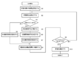
- FIG. 3 is a flowchart showing the processing of the board layout evaluation apparatus 4 of the present invention.
- a process executed by the CPU as the board layout evaluation device 4 will be described with reference to the flowchart of FIG.
- step S ⁇ b> 1 the CPU designates an evaluation target from among the wirings included in the layout data stored in the storage unit 3.
- the designated wiring is a wiring to be evaluated by the board layout evaluation device 4.
- the evaluation target designating unit 5 may accept the designation and set the designated wiring as the evaluation target. If it is troublesome for the designer to designate the evaluation target, all the wirings included in the layout data may be the evaluation target. Further, instead of letting the designer specify, the CPU may specify the evaluation object autonomously using the layout data.
- the net name which is the name of each wiring, is given, for example, a signal type including clock and data, signal standards such as USB and HDMI, characteristics such as signal operating frequency, names of components connected by wiring, etc. In many cases, it is regularized.
- step S2 the CPU performs processing as the passive component extraction unit 6 in FIG. That is, the passive component connected to the wiring designated as the evaluation target in step S1 is extracted.
- a component is a passive component can be determined from the first character string of the component name.
- the first character string such as R for resistance, C for capacitor, L for inductor, FB for ferrite bead, and CN for connector.
- the first character string such as IC for an integrated circuit, TR for a transistor, and D for a diode.
- the CPU extracts a resistor R 24 and a resistor R 28 as passive components connected to the wiring 22.
- step S3 the CPU determines whether the number of extracted passive components is 2 terminals or 4 terminals or more (hereinafter referred to as multi-terminal). When the passive component has three terminals, the electrical net is not searched.
- the layout data includes information on the number of terminals of each component. In FIG. 2, it is determined that the resistor R28 has two terminals and the resistor R24 has multiple terminals. Therefore, the routine proceeds to step S4.
- step S4 the CPU performs processing as the two-terminal EN search unit 7. That is, the extracted two-terminal passive component is searched for a wiring connected to a terminal different from the terminal connected to the wiring to be evaluated.
- the searched wiring is a constituent element of the electrical net including the evaluation target.
- the resistor terminal 28b is connected to the wiring 22.
- the CPU determines that the wiring 29 connected to the resistance terminal 28a different from the resistance terminal 28b of the resistor R28 is a constituent element of the electrical net.
- step S5 the CPU performs processing as the non-propagating terminal classification unit 9. That is, the extracted passive component terminals are classified. Classification is a process of grouping terminals that are normally considered not to be electrically connected to each other into the same class (non-propagating terminals). The terminals are classified according to the following logic. First, all the wiring connected to the terminal of the component is obtained. Then, other parts connected to these wirings (that is, parts excluding passive parts to be classified) are obtained. If there are two or more terminals connected to the same other parts via any wiring among the terminals of the passive parts to be classified, these are set as non-propagating terminals.
- the resistor R24 is a passive component that is focused on as a classification target.
- the wiring 22 connected to the resistance terminal 24a and the wiring 23 connected to the resistance terminal 24b are both connected to the integrated circuit IC21. That is, the resistance terminal 24 a is connected to the integrated circuit IC 21 that is another component via the wiring 22, and the resistance terminal 24 b is connected to the same other component via the wiring 23. Therefore, the CPU assumes that the resistance terminal 24a and the resistance terminal 24b are non-propagating terminals.
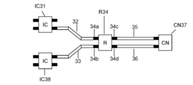
- FIG. 4 is an explanatory diagram showing an example of a board layout to be evaluated by the evaluation apparatus of the present invention.
- the integrated circuits IC31, IC38, resistor R34, and connector CN37 are connected by wirings 32, 33, 35, and 36.
- the integrated circuits IC31, IC38, resistor R34, and connector CN37 are connected by wirings 32, 33, 35, and 36.
- the resistance terminals 34c and 34d of the resistor R34 are non-propagating terminals because they are connected to the same connector CN37.
- the remaining resistance terminals 34a and 34b are not connected to the same component. However, they are non-propagating terminals.
- step S3 the passive component connected by the wiring to be evaluated is determined.
- non-propagating terminals can be determined in advance for all passive components. This method is convenient when there are a plurality of wirings to be evaluated and it is necessary to determine a non-propagating terminal for the same passive component many times. This is because it is possible to eliminate the waste of redundant determination processing for the same passive component.
- the CPU performs processing as a propagation candidate terminal determination unit 10.
- the terminal of the same component that is estimated to be electrically connected to the terminal of the passive component connected to the wiring to be evaluated is set as the propagation candidate terminal.
- the determination is made based on the shape of the part. That is, the x and y axes are set along the shape of the passive component. Both x and y axes are directions along the substrate. In a normal array component, terminals arranged so as to face each other along the x axis or the y axis are electrically connected to each other.
- the resistor terminals 24a and 24b along the y axis, the resistor terminals 24a and 24c, the resistor terminals 24a and 24c along the x axis, and the resistor terminals 24b and 24d are electrically connected, respectively.
- passive components to which the resistance terminals 24a and 24d and the resistance terminals 24b and 24c are electrically connected are not common. This is because it is generally costly to connect diagonal terminals such as the resistance terminals 24a and 24d and the resistance terminals 24b and 24c inside the resistor R24. When it is necessary to connect such terminals that do not conform to the shape of the component, it is natural to connect them by board wiring outside the component.
- the CPU sets a terminal arranged in a direction along the shape of the passive component as a propagation candidate terminal with respect to the passive component terminal connected to the wiring to be evaluated.
- resistance terminals 24 b and 24 c that are arranged in parallel along the component shape with the resistance terminal 24 a connected to the wiring 22 are propagation candidate terminals.
- step S7 the CPU performs processing as the EN search unit 11. That is, among the propagation candidate terminals for the terminals connected to the wiring 22, a wiring connected to a non-propagating terminal different from the target terminal is searched and determined as a constituent element of the electrical net.
- the component is handled as a wiring that constitutes an electrical net together with a wiring that is an evaluation target.
- the propagation candidate terminals of the resistance terminal 24a connected to the wiring 22 are the resistance terminals 24b and 24c.
- the resistance terminal 24b is a non-propagating terminal of the terminal resistance 24a. Therefore, the CPU determines that only the resistance terminal 24c belonging to a class different from the resistance terminal 24a is connected to the resistance terminal 24a via the resistor R24.
- the component of the electrical net including the wiring 22 is a wiring 25 connected to the resistance terminal 24c.
- FIG. 6 is an explanatory view showing an example of the shape of a component applicable to the present invention. According to the present invention, even if the resistance terminals 51a to 51d are not provided from the resistor R51 as shown in FIG. 6 and the terminals to be electrically connected are difficult to guess from the component shape, the components of the electrical net are searched. be able to. Further, even for a component whose layout data does not include information on the shape of the terminal, it is possible to estimate a terminal that is electrically connected within the component and to search for components of the electrical net.
- FIG. 7 is an explanatory view showing an example of a different board layout to be evaluated by the evaluation apparatus of the present invention.
- the integrated circuits IC61, IC67, IC68, IC69 and resistor R64 are connected by wirings 62, 63, 65 and 66.
- the wiring connected to the four terminals of the resistor R64 has no components connected in common.
- the non-propagating terminal classification unit 9 cannot classify the non-propagating terminals according to the logic described in step S5. If the non-propagating terminals cannot be classified, the constituent elements of the electrical net cannot be searched. In such a case, terminals are classified by the following alternative logic to search for constituent elements of the electrical net.
- the first alternative logic focuses on the width of the wiring connected to the terminal of the target passive component. Then, it is determined whether or not the widths of these wirings are divided into two types. When the width of the wiring is divided in two ways, it is determined that the terminals connected to the wiring having the same width are connected to each other via the passive component. When expressed in correspondence with the non-propagating terminal described in step S5, it is recognized that the terminals belong to different classes and do not have a non-propagating terminal relationship. That is, it is assumed that wirings having the same width are constituent elements of the same electrical net. For example, in the substrate layout shown in FIG.
- the widths of the wiring 62 and the wiring 63 are different, and the widths of the wiring 62 and the wiring 65 are equal.
- the CPU searches for a constituent element of the electrical net including the wiring 62, the CPU determines that the wiring 65 is the constituent element.
- the second alternative logic focuses on the net name.
- the net name is often given an attribute such as the type, standard, characteristic, and / or name of a component connected by the wiring. If the attribute information obtained from the net name is different for each net connected to each terminal, the terminals with the same attribute information for the net connected to the terminal are arranged in parallel along the part shape.
- a connection destination and a net to which the terminal is connected may be a constituent element of the electrical net.
- the processing of steps S5 to S7 in FIG. 3 can be similarly applied not only to the case where the passive component has four terminals but also to the passive component having a larger number of terminals.
- the terminals that should be considered to be electrically connected via the passive components are usually the terminals (target terminals) that are connected to the wiring subject to evaluation. It does not exist in the parallel terminal on the same side, but exists in a terminal arranged on a different side from the target terminal. For this reason, it is possible to search for a terminal to be regarded as being electrically connected via the passive component from the shape of the passive component.
- the logic for searching the electrical net for passive components with 6 terminals or more will be described below.
- FIG. 8 is an explanatory diagram showing the shape of the array resistor R71 as an example of a passive component having six or more terminals according to the present invention.
- the number of passive component terminals is 6 or more
- the resistance terminals 71a, 71b, 71c are arranged in the y-axis direction along the component shape.
- the number of terminals lined up is 4 or more.
- the CPU classifies the resistance terminals 71a, 71b, 71c as first non-propagating terminals. Similarly, the CPU classifies the resistance terminals 71d, 71e, 71f as second non-propagating terminals.
- the electrical net is searched based on the shape of the passive components even when all other components connected to the respective terminals via the net are different. be able to. As described above, the procedure for focusing on a certain wiring and setting it as an evaluation target and searching for a wiring that can form an electrical net together with the evaluation target has been described.
- step S8 the CPU determines whether or not the constituent elements of the electrical net found in steps S4 and S7, that is, the wiring includes power supply wiring and ground wiring.
- the CPU excludes the power supply wiring and the ground wiring from the constituent elements of the electrical net to be evaluated.
- the CPU may set power supply wiring and ground wiring in advance as wiring attributes.
- the power supply wiring and the ground wiring may be extracted from the net name.
- wiring that is frequently connected to the capacitor, wiring that has a certain thickness (width) and / or wiring that includes a planar area may be determined as power wiring or ground wiring and excluded.
- step S9 the CPU determines whether the search for the constituent elements of the electrical net has been completed for all of the designated evaluation targets. If there is a component that has not been searched for in the evaluation target specified in step S1, it is specified as a new evaluation target, and then the routine returns to step S2 to repeat the processing in steps S2 to S8. .
- FIG. 5 is an explanatory view showing still another example of the board layout to be evaluated by the evaluation apparatus of the present invention.
- the integrated circuit IC41, resistors R43 and R45, and connector CN47 are connected by wirings 42, 44, and 46, respectively.
- the wiring 42 is designated as the evaluation target in step S1 of FIG.
- step S9 the CPU searches for an electrical net including the wiring 42 and finds the wiring 44 as a component thereof. Thereafter, in step S9, the CPU adds the wiring 44 to the evaluation target. Then, the routine returns to S2 to search for further components of the electrical net with the evaluation object as the wiring 44. As a result, the CPU finds the wiring 46 as a component of the electrical net including the wiring 44. In subsequent step S9, the CPU adds the wiring 46 to the evaluation target. The routine then returns to S2 to search for further components of the electrical net including the wiring 46. However, a new component of the electrical net including the wirings 42, 44 and 46 is not found. Thereafter, in step S9, the CPU determines that the search for the electrical net has been completed. Finally, the wirings 42, 44 and 46 are the constituent elements of the electrical net. Then, the routine proceeds to step S10.
- step S10 the CPU evaluates whether or not the found electrical net has a board layout that does not become a radiation source with large unnecessary radiation noise. Evaluation indexes include the length of the wiring, the presence / absence of a guard wiring, and the presence / absence of a return current path.
- the evaluation of the length of the wiring length is to evaluate whether or not the total wiring length of the electrical net including the evaluation target exceeds a preset threshold value.
- a path length from the output terminal to another IC terminal or connector terminal may be obtained and used as an evaluation index.
- the path length is calculated as the length of the path of the electrical net.
- an IC terminal and a connector terminal connected to the electrical net may be extracted, and all the path lengths between the terminals may be obtained as an evaluation index.
- the evaluation of the presence / absence of guard wiring is performed by determining whether ground wiring as guard wiring is laid out on both sides of the wiring constituting the found electrical net. Whether the board layout is good or bad can be determined by using the total wiring length of the portion without the guard wiring as an evaluation index.
- the ground wiring in the evaluation of the presence or absence of the return current path, confirm whether the ground wiring is laid out in the adjacent layer of the found electrical net. Whether the board layout is good or not can be determined by using the total wiring length of the electrical net where there is no ground wiring as an evaluation index. However, even when there is no ground wiring in the adjacent layer, if the ground wiring is laid out on both sides of the wiring, the ground wiring can be a return path. Therefore, it is preferable to use the total wiring length of a portion where there is no ground wiring in the adjacent layer of the wiring that is a component of the electrical net and no ground wiring on both sides of the wiring as an evaluation index. By doing so, it is possible to determine whether the board layout is good or not including the case where return current paths are arranged on both sides of the wiring.
- the wiring length of the electrical net, the presence or absence of the guard wiring, and the presence or absence of the return current path are shown.
- the specific example of the evaluation in consideration of the electrical net is shown in the evaluation related to suppression of unnecessary radiation noise.
- the present invention is also effective for other uses. For example, even when a simulation of a signal transmitted on the determined board layout is performed, the signal simulation is usually performed in consideration of an electrical net.
- the electrical net can be searched by the procedure described with reference to FIG. That is, the electrical net is searched for signal simulation based on the shape of the part, the width of the wiring, and the net name without special specification by the designer or setting of the passing parameter of the part as in the prior art. be able to.
- the present invention it is possible to evaluate a board layout in consideration of an electrical net without requiring special settings such as passing parameters for each part. Designers do not have to spend time and effort on pre-configuration. Further, even when there are many wirings to be evaluated, the evaluation can be performed quickly and easily.
- the search method of the electrical net is applicable not only to the evaluation of the board layout but also to the signal simulation.
- Input unit 2 Layout generation unit 3: Storage unit 4: Board layout evaluation device 5: Evaluation target designating unit 6: Passive component extraction unit 7: Two-terminal electrical net search unit, Two-terminal EN search unit 8: Multi-terminal electrical Net search unit, multi-terminal EN search unit 9: non-propagation terminal classification unit 10: propagation candidate terminal determination unit 11: electrical net search unit, EN search unit 12: evaluation processing unit 13: output unit 14: layout data reference unit 15: Board layout design system IC21, IC30, IC31, IC38, IC41, IC61, IC67, IC68, IC69: integrated circuits 21a, 21b, 30a: IC terminals 22, 23, 25, 26, 29, 32, 33, 35, 36, 42, 44, 46, 62, 63, 65, 66: wirings CN27, CN37, CN47: connectors 27a, 27 : Connector terminals R24, R28, R34, R43, R45, R51, R64, R71: Resistors
Landscapes
- Engineering & Computer Science (AREA)
- Computer Hardware Design (AREA)
- Physics & Mathematics (AREA)
- Theoretical Computer Science (AREA)
- Evolutionary Computation (AREA)
- Geometry (AREA)
- General Engineering & Computer Science (AREA)
- General Physics & Mathematics (AREA)
- Design And Manufacture Of Integrated Circuits (AREA)
Abstract
部品を介して電気的につながっているとみなすべき配線を煩雑な設定なしに探索する。 評価対象の配線を指定する評価対象指定部と、その配線に接続される受動部品を抽出する受動部品抽出部と、その受動部品を介して信号が伝播する配線を探索する二端子エレクトリカルネット探索部および多端子エレクトリカルネット探索部と、探索された配線を考慮して基板レイアウトの評価を行う評価処理部とを備える。多端子エレクトリカルネット探索部は、多端子部品の外形形状に基づき評価対象配線に接続される端子に対する伝搬候補端子を決定し、前記伝搬候補端子のうち別の一つの部品に配線を介して共通に接続される複数の端子を一群の非伝搬端子とし、評価対象の配線に接続される端子を含む一群の非伝搬端子を前記伝搬候補端子から除き、残りの端子に接続される配線を評価対象に加える。
Description
この発明は、プリント基板のレイアウト評価装置および評価方法に関する。また、それを備えてなる基板レイアウト設計システムに関する。より詳細には、プリント基板上に設けられる信号配線、特にクロック信号やデータ信号に係る配線や部品のレイアウトが不要輻射ノイズ信号を抑制するよう考慮されているかを評価する基板レイアウト評価装置および評価方法、それを備えた基板レイアウト設計システムに関する。
近年、電子機器の高性能化に伴い、高速信号が伝送される配線を含んだプリント基板が多数用いられている。このような高速信号配線を含んだ回路基板のレイアウト設計においては、不要輻射ノイズを抑制するように考慮しつつ基板レイアウトを決定することが必要とされる。回路基板上の高速信号配線は、不要輻射ノイズを放射するアンテナの役割を果たし、ノイズの輻射源となってしまいやすい。高速信号配線の配線長が長くなるとノイズの輻射レベルが大きくなる。よって、高速信号配線についてその配線長をできる限り短くする基板レイアウトが望ましい。
また、高速信号配線のリターン電流経路が確保されていないと、ループする電流の経路が長くなってしまう。その結果、ノイズの輻射レベルが大きくなる。高速信号については、信号配線だけでなく、リターン電流経路にも留意した設計が重要である。
また、高速信号配線のリターン電流経路が確保されていないと、ループする電流の経路が長くなってしまう。その結果、ノイズの輻射レベルが大きくなる。高速信号については、信号配線だけでなく、リターン電流経路にも留意した設計が重要である。
さらに、高速信号配線に係る基板レイアウト設計では、部品の端子と端子を相互に接続する信号配線を考慮するだけでは不十分である。例えば信号線に直列に抵抗が挿入されていても、高速信号は、その抵抗を介して一方の配線から他の配線へ信号が伝播する。このように、部品を介して信号が伝播するとみなされる配線を、この明細書ではエレクトリカルネットと呼ぶ。高速信号配線の基板レイアウト設計では、エレクトリカルネットの配線長およびエレクトリカルネットのリターン電流経路を考慮して基板レイアウトを決定する必要がある。
プリント基板設計用のCAD(Computer Aided Design)システムにおいて、プリント基板に搭載する各種部品の配置や配線パターン等のレイアウトは、レイアウトデータによって定義される。前記レイアウトデータは、レイアウト設計者が回路図データを元にCADシステム上で基板レイアウト設計を行うことによって、生成されるデータである。近年、生成されたレイアウトデータが、不要輻射ノイズを抑える設計となっているかを評価する機能がある。
この評価機能は、CADに付随するものとして、あるいは、CADと独立したものとして提供される。前記評価機能は、レイアウトデータで定義されるプリント基板のレイアウトにおいて、高速信号配線の配線長が短く設計されているかを評価する、前記配線長は、前述のごとくエレクトリカルネットを考慮する。信号配線中に例えば抵抗が直列接続されている場合、抵抗を介して接続される2つの高速信号配線を合わせた配線の経路長を算出し評価する。
この評価機能は、CADに付随するものとして、あるいは、CADと独立したものとして提供される。前記評価機能は、レイアウトデータで定義されるプリント基板のレイアウトにおいて、高速信号配線の配線長が短く設計されているかを評価する、前記配線長は、前述のごとくエレクトリカルネットを考慮する。信号配線中に例えば抵抗が直列接続されている場合、抵抗を介して接続される2つの高速信号配線を合わせた配線の経路長を算出し評価する。
このようなエレクトリカルネットを考慮した配線長を算出する技術として、ある配線(ネット)上で指定された算出開始ポイントから、同一の又は異なる配線上で指定された算出終了ポイントに至る配線の経路長を算出するシステムが知られている。ここで「ネット」は、「エレクトリカルネット」とは意味が異なる。この明細書で単なる「ネット」は、部品を介さずに電気的につながっている個々の配線を指す。エレクトリカルネットは、部品を介して信号が伝播するとみなされ、従って、電気的につながっているとみなすべき複数の配線であって、ネットの集合である。
前述の配線長算出システムは、それぞれの電子部品の情報を通過パラメータとして予め記録している。前記通過パラメータは、プリント配線板に実装する電子部品が配線経路を探索するうえでどの端子からどの端子へと配線経路を通過させると見なすかを規定した通過端子情報である。配線経路を検索する際、この通過パラメータに基づいて所定の電子部品の一の端子から他の端子へと配線経路を通過させるか否かを判断する。この配線長算出システムによれば、異なるネットに存在する所定ポイント間の配線経路についてその配線の経路長が算出可能である。そして、算出された経路長が規定した範囲内に収まっているかを検査する(例えば、特許文献1参照)。
例えば、経路長を算出すべき一のポイント(電子部品の端子)から他のポイント(電子部品の端子)の間に抵抗が存在する場合を考える。抵抗の通過パラメータは、通過可能と記録されている。前記配線長算出システムは、一のポイントから他のポイントまで配線経路が存すると判断し、その配線経路の経路長を算出する。
前述の配線長算出システムは、それぞれの電子部品の情報を通過パラメータとして予め記録している。前記通過パラメータは、プリント配線板に実装する電子部品が配線経路を探索するうえでどの端子からどの端子へと配線経路を通過させると見なすかを規定した通過端子情報である。配線経路を検索する際、この通過パラメータに基づいて所定の電子部品の一の端子から他の端子へと配線経路を通過させるか否かを判断する。この配線長算出システムによれば、異なるネットに存在する所定ポイント間の配線経路についてその配線の経路長が算出可能である。そして、算出された経路長が規定した範囲内に収まっているかを検査する(例えば、特許文献1参照)。
例えば、経路長を算出すべき一のポイント(電子部品の端子)から他のポイント(電子部品の端子)の間に抵抗が存在する場合を考える。抵抗の通過パラメータは、通過可能と記録されている。前記配線長算出システムは、一のポイントから他のポイントまで配線経路が存すると判断し、その配線経路の経路長を算出する。
特許文献1の配線長算出システムによれば、配線基板上の異なるネットを対象に配線長を算出できるが、ネットに接続された部品全てについて通過パラメータを予め設定しておく必要がある。通過パラメータの事前設定に労力を要する。通過パラメータを含むライブラリが一旦完成した後は、そのライブラリを用いて配線長を算出することができる。即ち、基板レイアウト設計を行う度にパラメータを設定する必要はなくなる。その一方で、前記ライブラリが適用可能な環境でしか確認を行うことができない。即ち、前記ライブラリが適用できない環境、例えば、他のCADで設計された基板は、評価を行うことができない。
本発明は、以上のような事情を考慮してなされたものであって、部品に通過パラメータのような煩雑な事前設定を行わなくてもエレクトリカルネットを探索し、見出されたエレクトリカルネットを考慮して基板レイアウトの評価を行うことのできる基板レイアウト評価装置を提供するものである。また、対応する評価方法および前記評価装置を備えてなる基板レイアウト設計システムを提供するものである。
本発明は、以上のような事情を考慮してなされたものであって、部品に通過パラメータのような煩雑な事前設定を行わなくてもエレクトリカルネットを探索し、見出されたエレクトリカルネットを考慮して基板レイアウトの評価を行うことのできる基板レイアウト評価装置を提供するものである。また、対応する評価方法および前記評価装置を備えてなる基板レイアウト設計システムを提供するものである。
この発明は、プリント基板の配線および前記配線により接続される部品についてのレイアウトデータを参照するレイアウトデータ参照部と、前記レイアウトデータに含まれる配線のうちで評価対象とすべき配線を指定する評価対象指定部と、評価対象とされた配線に接続される受動部品を抽出する受動部品抽出部と、抽出された受動部品の中に2端子部品がある場合、その2端子部品を介して評価対象の配線の一つと接続された配線である二端子エレクトリカルネットを探索する二端子エレクトリカルネット探索部と、抽出された受動部品の中に4以上の端子を有する多端子部品がある場合、その多端子部品を介して評価対象の配線の一つから信号が伝播するとみなすべき配線である多端子エレクトリカルネットを探索する多端子エレクトリカルネット探索部と、探索された配線を用いて基板レイアウトの評価を行う評価処理部とを備え、前記多端子エレクトリカルネット探索部は、前記受動部品の外形形状に基づき、その受動部品の端子のうちで評価対象の配線の一つに接続される端子と同じ側にある端子または反対側の対向する位置にある端子を伝搬候補端子とし、前記伝搬候補端子のうち別の一つの部品に配線を介して共通に接続される複数の端子がある場合、それらの端子を一群の非伝搬端子とし、評価対象の配線に接続される端子を含む一群の非伝搬端子を前記伝搬候補端子から除いて伝搬端子とし、その伝搬端子に接続される配線を前記多端子エレクトリカルネットとし、前記評価処理部は、評価対象の配線並びに前記二端子エレクトリカルネットおよび/または前記多端子エレクトリカルネットの集合としてのエレクトリカルネットの配線長、前記エレクトリカルネットの両側にガード配線が配置されているか否か、および/または、前記エレクトリカルネットに係る信号のリターン電流経路が配置されているか否かを指標として前記基板レイアウトの評価を行う基板レイアウト評価装置を提供する。
換言すれば、前記二端子エレクトリカルネット検索部は、抽出された受動部品の中に端子数が2端子のものがある場合、その2端子の受動部品を介して評価対象の配線から信号が伝播するとみなすべき配線を探索するものである。また、前記多端子エレクトリカルネット探索部は、抽出された受動部品の中に端子数が4端子以上のものがある場合、その4端子以上の受動部品を介して評価対象の配線から信号が伝播するとみなすべき配線を探索するものである。詳細には、前記二端子エレクトリカルネット探索部は、評価対象の配線に接続される端子と異なる端子に接続される他の配線に、評価対象に指定された配線から信号が伝播するとみなして他の配線を評価対象に加える。前記多端子エレクトリカルネット探索部は、前記受動部品の各端子のうち配線を介してその受動部品以外の同一部品に接続される複数の端子がある場合、それらの端子を同じ組の非伝搬端子として分類する。さらに、前記受動部品の外形形状に基づき、評価対象とされた配線に接続される対象端子と同じ側に並ぶ端子および前記対象端子と反対側で対向する位置にある端子を伝搬候補端子とし、それら伝搬候補端子のうち前記対象端子と同じ組の非伝搬端子ではない端子を伝搬端子とする。そして、伝搬端子に接続される配線を評価対象に加える。前記評価処理部は、前記評価対象指定部により指定された配線並びに前記二端子エレクトリカルネット探索部配線および/または前記多端子エレクトリカルネット探索部によって評価対象に加えられた配線からなる集合をエレクトリカルネットとする。
換言すれば、前記二端子エレクトリカルネット検索部は、抽出された受動部品の中に端子数が2端子のものがある場合、その2端子の受動部品を介して評価対象の配線から信号が伝播するとみなすべき配線を探索するものである。また、前記多端子エレクトリカルネット探索部は、抽出された受動部品の中に端子数が4端子以上のものがある場合、その4端子以上の受動部品を介して評価対象の配線から信号が伝播するとみなすべき配線を探索するものである。詳細には、前記二端子エレクトリカルネット探索部は、評価対象の配線に接続される端子と異なる端子に接続される他の配線に、評価対象に指定された配線から信号が伝播するとみなして他の配線を評価対象に加える。前記多端子エレクトリカルネット探索部は、前記受動部品の各端子のうち配線を介してその受動部品以外の同一部品に接続される複数の端子がある場合、それらの端子を同じ組の非伝搬端子として分類する。さらに、前記受動部品の外形形状に基づき、評価対象とされた配線に接続される対象端子と同じ側に並ぶ端子および前記対象端子と反対側で対向する位置にある端子を伝搬候補端子とし、それら伝搬候補端子のうち前記対象端子と同じ組の非伝搬端子ではない端子を伝搬端子とする。そして、伝搬端子に接続される配線を評価対象に加える。前記評価処理部は、前記評価対象指定部により指定された配線並びに前記二端子エレクトリカルネット探索部配線および/または前記多端子エレクトリカルネット探索部によって評価対象に加えられた配線からなる集合をエレクトリカルネットとする。
また、異なる観点から、この発明は、コンピュータが、プリント基板の配線および前記配線により接続される部品についてのレイアウトデータを参照するステップと、前記レイアウトの情報に基づいて評価対象とすべき配線を指定するか、前記レイアウトデータに含まれる配線のうちで評価対象とすべき配線のユーザーによる指定を受け付けるステップと、評価対象とされた配線に接続される受動部品を抽出するステップと、抽出された受動部品の中に2端子部品がある場合、その2端子の受動部品を介して評価対象の配線の一つと接続された配線である二端子エレクトリカルネットを探索する二端子エレクトリカルネット探索ステップと、抽出された受動部品の中に4以上の端子を有する多端子部品がある場合、その多端子部品を介して評価対象の配線の一つから信号が伝播するとみなすべき配線である多端子エレクトリカルネットを探索する多端子エレクトリカルネット探索ステップと、探索された配線を用いて基板レイアウトの評価を行う評価ステップとを備え、前記多端子エレクトリカルネット探索ステップは、前記受動部品の外形形状に基づき、その受動部品の端子のうちで評価対象の配線の一つに接続される端子と同じ側にある端子または反対側の対向する位置にある端子を伝搬候補端子とし、前記伝搬候補端子のうち別の一つの部品に配線を介して共通に接続される複数の端子がある場合、それらの端子を一群の非伝搬端子とし、評価対象の配線に接続される端子を含む一群の非伝搬端子を前記伝搬候補端子から除いて伝搬端子とし、その伝搬端子に接続される配線を前記多端子エレクトリカルネットとし、前記評価ステップは、評価対象の配線並びに前記二端子エレクトリカルネットおよび/または前記多端子エレクトリカルネットの集合としてのエレクトリカルネットの配線長、前記エレクトリカルネットの両側にガード配線が配置されているか否か、および/または、前記エレクトリカルネットに係る信号のリターン電流経路が配置されているか否かを指標として前記基板レイアウトの評価を行う基板レイアウトの評価方法を提供する。
換言すれば、前記二端子エレクトリカルネット検索ステップは、抽出された受動部品の中に端子数が2端子のものがある場合、その2端子の受動部品を介して評価対象の配線から信号が伝播するとみなすべき配線を探索するステップである。また、前記多端子エレクトリカルネット探索ステップは、抽出された受動部品の中に端子数が4端子以上のものがある場合、その4端子以上の受動部品を介して評価対象の配線から信号が伝播するとみなすべき配線を探索するステップである。詳細には、前記二端子エレクトリカルネット探索ステップは、評価対象の配線に接続される端子と異なる端子に接続される他の配線に、評価対象に指定された配線から信号が伝播するとみなして他の配線を評価対象に加える。前記多端子エレクトリカルネット探索ステップは、前記受動部品の各端子のうち配線を介してその受動部品以外の同一部品に接続される複数の端子がある場合、それらの端子を同じ組の非伝搬端子として分類する。さらに、前記受動部品の外形形状に基づき、評価対象とされた配線に接続される対象端子と同じ側に並ぶ端子および前記対象端子と反対側で対向する位置にある端子を伝搬候補端子とし、それら伝搬候補端子のうち前記対象端子と同じ組の非伝搬端子ではない端子を伝搬端子とする。そして、伝搬端子に接続される配線を評価対象に加える。前記評価ステップは、前記評価対象指定部により指定された配線並びに前記二端子エレクトリカルネット探索部配線および/または前記多端子エレクトリカルネット探索部によって評価対象に加えられた配線からなる集合をエレクトリカルネットとする。
換言すれば、前記二端子エレクトリカルネット検索ステップは、抽出された受動部品の中に端子数が2端子のものがある場合、その2端子の受動部品を介して評価対象の配線から信号が伝播するとみなすべき配線を探索するステップである。また、前記多端子エレクトリカルネット探索ステップは、抽出された受動部品の中に端子数が4端子以上のものがある場合、その4端子以上の受動部品を介して評価対象の配線から信号が伝播するとみなすべき配線を探索するステップである。詳細には、前記二端子エレクトリカルネット探索ステップは、評価対象の配線に接続される端子と異なる端子に接続される他の配線に、評価対象に指定された配線から信号が伝播するとみなして他の配線を評価対象に加える。前記多端子エレクトリカルネット探索ステップは、前記受動部品の各端子のうち配線を介してその受動部品以外の同一部品に接続される複数の端子がある場合、それらの端子を同じ組の非伝搬端子として分類する。さらに、前記受動部品の外形形状に基づき、評価対象とされた配線に接続される対象端子と同じ側に並ぶ端子および前記対象端子と反対側で対向する位置にある端子を伝搬候補端子とし、それら伝搬候補端子のうち前記対象端子と同じ組の非伝搬端子ではない端子を伝搬端子とする。そして、伝搬端子に接続される配線を評価対象に加える。前記評価ステップは、前記評価対象指定部により指定された配線並びに前記二端子エレクトリカルネット探索部配線および/または前記多端子エレクトリカルネット探索部によって評価対象に加えられた配線からなる集合をエレクトリカルネットとする。
さらに、この発明は前記基板レイアウト評価装置と、基板レイアウト設計に関するユーザーからの指示を受け付ける入力部と、入力された指示に基づいてレイアウトデータを生成するレイアウト生成部と、生成されたレイアウトデータを記憶する記憶部と、前記レイアウトデータが表すレイアウト、および、前記レイアウトの前記基板レイアウト評価装置による評価を出力する出力部とを備えてなる基板レイアウト設計システムを提供する。
この発明の基板レイアウト評価装置において、前記二端子エレクトリカルネット探索部は、2端子部品を介して評価対象の配線の一つと接続された配線に、評価対象の配線から信号が伝播するとみなして他の配線を評価対象に加え、前記多端子エレクトリカルネット探索部は、前記受動部品の各端子のうちで評価対象の配線の一つに接続される端子と同じ側にある端子または反対側の対向する位置にある端子を伝搬候補端子とし、前記伝搬候補端子のうち別の一つの部品に配線を介して共通に接続される複数の端子がある場合、それらの端子を一群の非伝搬端子とし、評価対象の配線に接続される端子を含む一群の非伝搬端子を前記伝搬候補端子から除いて伝搬端子とし、その伝搬端子に接続される配線を評価対象に加えるので、部品に通過パラメータのような煩雑な事前設定を行わなくても評価対象の配線から信号が伝搬するエレクトリカルネットを探索し、見出されたエレクトリカルネットを考慮して基板レイアウトの評価を行うことができる。
この発明による評価方法および基板レイアウト設計システムも同様の作用効果を奏する。
この発明による評価方法および基板レイアウト設計システムも同様の作用効果を奏する。
この発明の基板レイアウト評価装置は、基板レイアウト設計に用いられるCADシステムの一部として組み入れられて構成することができる。
この発明において、プリント基板は、単層または多層の配線層を有し、基板上に搭載される部品を配線により電気的に接続して所定の機能を有する電子回路を実現するための基板である。CADによる基板レイアウト設計の対象となるものであれば、基板の材質や形状は問わない。よって、平板状の基板に限らず、屈曲に耐え柔軟性のあるフィルム状のものも含む。その典型的な態様としては、パーソナルコンピュータや携帯情報端末のマザーボードが挙げられるが、それらに限定されるものではない。
この発明において、プリント基板は、単層または多層の配線層を有し、基板上に搭載される部品を配線により電気的に接続して所定の機能を有する電子回路を実現するための基板である。CADによる基板レイアウト設計の対象となるものであれば、基板の材質や形状は問わない。よって、平板状の基板に限らず、屈曲に耐え柔軟性のあるフィルム状のものも含む。その典型的な態様としては、パーソナルコンピュータや携帯情報端末のマザーボードが挙げられるが、それらに限定されるものではない。
配線は、基板の表面あるいは基板内部に形成される配線層内にあって、ある点と他の点との間を電気的に接続する導体である。典型的には線状のものであるが、接地配線や電源配線は、広い幅を有する「面」領域として実装されることがある。
部品は、回路を構成する電子部品である。部品は、能動部品と受動部品に大別される。能動部品は、信号以外のエネルギーを信号エネルギーに変換したり増幅したりする機能を含む部品である。受動部品の例としては、抵抗、コンデンサ、インダクタ、コモンモードチョークコイル、フェライトビーズ、コネクタが挙げられる。これに対し、能動部品の例としては、IC(集積回路)、トランジスタ、ダイオードが挙げられる。各部品は、基板上の配線と接続するための端子を有する。通常、部品の端子数は、2以上である。
部品は、回路を構成する電子部品である。部品は、能動部品と受動部品に大別される。能動部品は、信号以外のエネルギーを信号エネルギーに変換したり増幅したりする機能を含む部品である。受動部品の例としては、抵抗、コンデンサ、インダクタ、コモンモードチョークコイル、フェライトビーズ、コネクタが挙げられる。これに対し、能動部品の例としては、IC(集積回路)、トランジスタ、ダイオードが挙げられる。各部品は、基板上の配線と接続するための端子を有する。通常、部品の端子数は、2以上である。
また、レイアウトは、レイアウトデータとして記憶部に記憶される。レイアウトデータは、通常、プリント基板設計用のCADにより生成される。レイアウトデータは、基板上に配置すべき配線について、それらの位置、経路、形状、幅(配線の太さ)などの情報を含む。さらに、基板上に配置されるべき部品の位置、形状、受動部品か能動部品かの種別、端子の配置および数などの情報を含む。
記憶部は、レイアウト生成部によって作成されたレイアウトデータを格納する記憶装置である。その具体的な態様としては、ハードディスクドライブ装置やフラッシュメモリ(ソリッドステートドライブとしてアレイ化されていてもよい)が挙げられる。
評価対象指定部の機能は、評価対象の配線を指定するために用いられるキーボードやマウスの入力インターフェイス回路およびその回路の制御をCPUに実行させる処理プログラムによって実現されてもよい。あるいは、CPUがレイアウトデータに基づいて自律的に評価対象を指定する場合、評価対象指定部の機能は前記CPUが実行する処理プログラムによって実現される。両方の態様が包含されてもよい。
評価対象指定部の機能は、評価対象の配線を指定するために用いられるキーボードやマウスの入力インターフェイス回路およびその回路の制御をCPUに実行させる処理プログラムによって実現されてもよい。あるいは、CPUがレイアウトデータに基づいて自律的に評価対象を指定する場合、評価対象指定部の機能は前記CPUが実行する処理プログラムによって実現される。両方の態様が包含されてもよい。
また、受動部品抽出部、二端子エレクトリカルネット探索部、多端子エレクトリカルネット探索部および評価処理部の機能は、CPUが前記レイアウトデータを参照しつつ処理を行うことによって実現されるものである。より詳細には、CPUに基板レイアウトの評価処理を実行させるプログラム、そのプログラムを実行するCPUおよびそのCPUが読み取り可能に前記プログラムを格納する記憶装置によりその機能が実現される。この明細書のCPUは、単独のものでもよいが、複数のCPUが協働して処理を実行する態様でもよい。その一例は、いわゆるクラウド・コンピューティングおよびグリッド・コンピューティングと呼ばれる態様などである。
受動部品を介して信号が伝播するとは、評価対象の配線の信号、即ち、その配線の電位あるいはその配線に流れる電流が変化すると、その配線に接続される受動部品の端子から他の端子へその変化が伝わり、他の端子に接続される配線に同様の電位的変化あるいは電流の変化が生じることである。即ち、他の端子に接続される配線も不要輻射ノイズの輻射源となることである。能動部品は自ら信号を駆動するが、受動部品は受動的に信号を伝達する。この発明では、そのような受動部品の特性に着目し、受動部品を介して不要輻射ノイズが伝搬する配線を探索し、それらを含めた配線の集合であるエレクトリカルネットについて、不要輻射ノイズの抑制を考慮したレイアウトが得られているか否かを評価するのである。
部品の外形形状は、主にパッケージの外形とそのパッケージ上の端子の配置に係る形状である。伝搬候補端子は、受動部品内部で信号が交差するように接続されることはないという着想に基づいて決定される。非伝搬端子は、外部で同一の部品に接続される端子は、異なる信号線であるという着想に基づいて決定される。
なお、非伝搬端子については、それ以外に、配線の幅の異同、ネット名から得られる信号の属性、6端子以上の場合は通常内部でストレートに接続されるのでパッケージの異なる側にある端子どうしが接続されるといった前提に基づいて決定してもよい。
なお、非伝搬端子については、それ以外に、配線の幅の異同、ネット名から得られる信号の属性、6端子以上の場合は通常内部でストレートに接続されるのでパッケージの異なる側にある端子どうしが接続されるといった前提に基づいて決定してもよい。
また、評価処理部は、探索されたエレクトリカルネットの配線長、ガード配線の有無および/またはリターン電流経路の有無を指標に評価を行う。配線長は、不要輻射ノイズを放射するアンテナ、即ち輻射源の大きさに関連する点を考慮したものである。ガード配線は、エレクトリカルネットの両側の近傍に接地配線等、定電位の配線を配置することによって得られるノイズのシールド(遮蔽)効果を考慮したものである。リターン電流経路は、信号の往路のみでなく復路を含めた経路長、即ち、電流ループの経路長あるいは電流ループの内部面積が、輻射源の大きさに関連する点を考慮したものである。信号の復路は、接地配線あるいは電源配線で構成される。
以下、この発明の好ましい態様について説明する。
前記二端子エレクトリカルネット探索部および前記多端子エレクトリカルネット探索部は、いずれも、探索により得た配線が電源または接地配線の場合、その配線を評価対象から除外するようにしてもよい。このようにすれば、一定の電圧が維持され、不要輻射ノイズの発生源にならないと考えられる電源および接地配線をエレクトリカルネットから除外することができるので、より正確な評価を行うことができる。
前記二端子エレクトリカルネット探索部および前記多端子エレクトリカルネット探索部は、いずれも、探索により得た配線が電源または接地配線の場合、その配線を評価対象から除外するようにしてもよい。このようにすれば、一定の電圧が維持され、不要輻射ノイズの発生源にならないと考えられる電源および接地配線をエレクトリカルネットから除外することができるので、より正確な評価を行うことができる。
また、前記二端子エレクトリカルネット探索部および前記多端子エレクトリカルネット探索部は、いずれも、探索により得た配線を評価対象に加え、加えられた評価対象の配線について、さらに探索を行うようにしてもよい。このようにすれば、探索により得た配線から、受動部品を介してさらに信号が伝播する配線を評価対象に加えることができるので、より正確な評価を行うことができる。
さらにまた、前記多端子エレクトリカルネット探索部は、ある受動部品に一組以上の非伝搬端子が存在するが、どの組にも属さない複数の端子があるとき、どの組にも属さない端子を一組の非伝搬端子としてもよい。
前記多端子エレクトリカルネット探索部は、6端子以上の受動部品について、部品形状に基づき同じ辺に沿って並ぶ3以上の端子を一組の非伝搬端子としてもよい。このようにすれば、受動部品の形状に基づいて被伝搬端子を決定できるので、配線の接続関係から被伝搬端子を決めることができない場合でもエレクトリカルネットを探索することができる。
また、前記評価処理部は、前記エレクトリカルネットの総配線長を予め定められた閾値と比較し、評価指標に用いてもよい。このようにすれば、不要輻射ノイズの発生源となるエレクトリカルネットの総配線長を用いて評価を行うことができる。
さらにまた、前記評価処理部は、評価対象とされた配線の両側にシールド用接地配線が配置されていない部分の経路長を算出し、評価指標に用いてもよい。このようにすれば、シールド用接地配線によって不要輻射ノイズが抑制される効果を考慮できるので、より正確な評価を行うことができる。
あるいは、前記プリント基板が多層基板であり、前記評価処理部は、評価対象とされた配線が存する配線層の隣接層に、前記配線に対応する接地領域または接地配線が配置されていない部分の経路長を算出し、評価指標に用いてもよい。このようにすれば、隣接層の接地配線によって不要輻射ノイズが抑制される効果を考慮できるので、より正確な評価を行うことができる。
あるいはまた、前記評価処理部は、評価対象とされた配線が存する配線層の隣接層の接地配線がないか、あるいは、隣接層があっても前記配線に対応する接地領域または接地配線がない部分、および、前記配線の両側に接地配線が配置されていない部分の経路長を算出し、評価指標に用いてもよい。このようにすれば、隣接層の接地配線または両側の接地配線によって不要輻射ノイズが抑制される効果を考慮できるので、より正確な評価を行うことができる。
ここで示した種々の好ましい態様は、それら複数を組み合わせることもできる。
ここで示した種々の好ましい態様は、それら複数を組み合わせることもできる。
以下、図面を用いてこの発明をさらに詳述する。なお、以下の説明は、すべての点で例示であって、この発明を限定するものと解されるべきではない。
≪基板レイアウト評価装置の全体的な構成≫
図1は、本発明の実施形態である基板レイアウト評価装置を示す構成ブロック図である。本発明の基板レイアウト評価装置4は、基板レイアウト設計に用いられる基板レイアウト設計システム15の一部に組み入れられて構成することができる。
≪基板レイアウト評価装置の全体的な構成≫
図1は、本発明の実施形態である基板レイアウト評価装置を示す構成ブロック図である。本発明の基板レイアウト評価装置4は、基板レイアウト設計に用いられる基板レイアウト設計システム15の一部に組み入れられて構成することができる。
この発明の基板レイアウト設計システムは、入力部1、レイアウト生成部2、記憶部3、基板レイアウト評価装置4および出力部13を備えてなる。
この発明の基板レイアウト評価装置4は、評価対象指定部5、受動部品抽出部6、二端子エレクトリカルネット探索部7(以下、略して二端子EN探索部と記す)、多端子エレクトリカルネット探索部8(以下、略して多端子EN探索部と記す)、評価処理部12およびレイアウトデータ参照部14を備える。
この発明の基板レイアウト評価装置4は、評価対象指定部5、受動部品抽出部6、二端子エレクトリカルネット探索部7(以下、略して二端子EN探索部と記す)、多端子エレクトリカルネット探索部8(以下、略して多端子EN探索部と記す)、評価処理部12およびレイアウトデータ参照部14を備える。
さらに、多端子EN探索部8は、非伝搬端子分類部9、伝搬候補端子決定部10およびエレクトリカルネット探索部11(以下、略してEN探索部と記す)を含む。
入力部1は、設計者がキーボードやマウス等を用いて、基板レイアウト設計に必要な情報を入力する操作に応答して、入力された情報を受け付ける。その具体的な態様は、入力の操作に用いられるキーボードやマウス等ハードウェアとのインターフェイスを担うインターフェイス回路およびそのインターフェイス回路を制御するソフトウェアである。
この発明の評価対象指定部は、特にユーザーが評価対象の配線を指定する場合、入力部1を構成に含む。
入力部1は、設計者がキーボードやマウス等を用いて、基板レイアウト設計に必要な情報を入力する操作に応答して、入力された情報を受け付ける。その具体的な態様は、入力の操作に用いられるキーボードやマウス等ハードウェアとのインターフェイスを担うインターフェイス回路およびそのインターフェイス回路を制御するソフトウェアである。
この発明の評価対象指定部は、特にユーザーが評価対象の配線を指定する場合、入力部1を構成に含む。
レイアウト生成部2は、CPUに基板レイアウト設計の処理を実行させるためのプログラム、そのプログラムを実行するCPUおよびそのCPUが読み取り可能に前記処理プログラムを格納する記憶装置によりその機能が実現される。なお、前述のCPU、記憶装置を提供するハードウェアの具体的態様の例として、パーソナルコンピュータやネットワークサーバーが挙げられる。レイアウト生成部2は、入力された情報に基づいて基板レイアウトを作成し、レイアウトデータを出力する。この発明の評価装置が基板レイアウト設計用のCADから独立している場合、レイアウト生成部2は構成に含まれない。
記憶部3は、レイアウト生成部2によって作成されたレイアウトデータを格納する記憶装置である。その具体的な態様としては、ハードディスクドライブ装置やフラッシュメモリ(ソリッドステートドライブとしてアレイ化されていてもよい)が挙げられる。前記記憶部3は、レイアウトデータに加えて、CPUが実行すべき基板レイアウト設計のプログラムを格納してもよい。
基板レイアウト評価装置4は、CPUに基板レイアウトの評価処理を実行させるプログラム、そのプログラムを実行するCPUおよびそのCPUが読み取り可能に前記プログラムを格納する記憶装置によりその機能が実現される。前記プログラムは、記憶部3に格納されてもよいが、別の記憶装置に格納されてもよい。なお、前述のCPU、記憶装置を提供するハードウェアは、レイアウト生成部2と共通のものであってもよいが、別のハードウェアであってもよい。即ち、基板レイアウト設計を行うものと共通のコンピュータやネットワークサーバーを用いてもよいが、異なるコンピュータやネットワークサーバーを用いてもよい。
出力部13は、基板レイアウト評価装置4で評価された結果を出力する。具体的には、出力部13は、評価の結果を出力するための表示装置、その表示装置を動作させるためのインターフェイス回路および前記インターフェイス回路の制御をCPUに実行させる処理プログラムを含んで構成される。
出力部13は、基板レイアウト評価装置4で評価された結果を出力する。具体的には、出力部13は、評価の結果を出力するための表示装置、その表示装置を動作させるためのインターフェイス回路および前記インターフェイス回路の制御をCPUに実行させる処理プログラムを含んで構成される。
図1に示す例は、基板レイアウト設計と基板レイアウト評価装置に共通のハードウェアを用いている。もっとも、基板レイアウト設計とその評価に用いるハードウェアが共通か否かを問わず、基板レイアウト評価装置4は、レイアウト生成部2により生成されたレイアウトデータに基づいて評価を行う。その評価は、レイアウト生成部2によりなされた基板のレイアウトが、不要輻射ノイズの発生を抑えるような設計になっているかを確認するものである。
≪基板レイアウト評価装置の構成≫
以下、基板レイアウト評価装置4の構成を説明する。
評価対象指定部5は、レイアウトデータの中から評価すべき配線を評価対象として指定する。
受動部品抽出部6は、レイアウトデータの中から指定された配線と接続されている受動部品を抽出する。ここで、受動部品は、能動部品以外の部品を指す。
二端子EN探索部7は、抽出した受動部品が2端子の部品の場合に、評価対象とされた配線と共にエレクトリカルネットを構成する配線を探索する。
多端子EN探索部8は、抽出された受動部品が4端子以上の場合に、評価対象とされた配線と共にエレクトリカルネットを構成する配線を探索する。
以下、基板レイアウト評価装置4の構成を説明する。
評価対象指定部5は、レイアウトデータの中から評価すべき配線を評価対象として指定する。
受動部品抽出部6は、レイアウトデータの中から指定された配線と接続されている受動部品を抽出する。ここで、受動部品は、能動部品以外の部品を指す。
二端子EN探索部7は、抽出した受動部品が2端子の部品の場合に、評価対象とされた配線と共にエレクトリカルネットを構成する配線を探索する。
多端子EN探索部8は、抽出された受動部品が4端子以上の場合に、評価対象とされた配線と共にエレクトリカルネットを構成する配線を探索する。
以下、多端子EN探索部8の下位の構成を説明する。
非伝搬端子分類部9は、端子に接続されているそれぞれの配線が同じ部品(抽出された受動部品を除く)に接続される端子を非伝搬端子として分類する。
伝搬候補端子決定部10は、部品形状から評価対象とされた配線に接続した端子と電気的に接続している可能性のある端子を決定する。
EN探索部11は、抽出した伝搬候補端子の中で評価対象とされた配線と接続された端子と異なる非伝搬端子に接続さている配線を、評価対象を含むエレクトリカルネットの構成要素であると判断する。
非伝搬端子分類部9は、端子に接続されているそれぞれの配線が同じ部品(抽出された受動部品を除く)に接続される端子を非伝搬端子として分類する。
伝搬候補端子決定部10は、部品形状から評価対象とされた配線に接続した端子と電気的に接続している可能性のある端子を決定する。
EN探索部11は、抽出した伝搬候補端子の中で評価対象とされた配線と接続された端子と異なる非伝搬端子に接続さている配線を、評価対象を含むエレクトリカルネットの構成要素であると判断する。
基板レイアウト評価装置4の構成に戻る。
評価処理部12は、見出されたエレクトリカルネットを考慮しつつ、基板レイアウトが不要輻射ノイズを抑えるような設計になっているかを評価する。
レイアウトデータ参照部14は、記憶部3に記憶されたレイアウトデータを参照する。評価対象指定部5、受動部品抽出部6、二端子EN探索部7、多端子EN探索部8および評価処理部12は、レイアウトデータ参照部14を介して処理に必要なレイアウトデータを参照する。
評価処理部12は、見出されたエレクトリカルネットを考慮しつつ、基板レイアウトが不要輻射ノイズを抑えるような設計になっているかを評価する。
レイアウトデータ参照部14は、記憶部3に記憶されたレイアウトデータを参照する。評価対象指定部5、受動部品抽出部6、二端子EN探索部7、多端子EN探索部8および評価処理部12は、レイアウトデータ参照部14を介して処理に必要なレイアウトデータを参照する。
≪具体的な基板レイアウトへの適用例≫
図2は、本発明の評価装置が評価対象とする基板レイアウトの一例を示す説明図である。図2の基板レイアウトは、集積回路IC21、IC30、抵抗R24、R28、コネクタCN27を配線22、23、25、26および29で接続するものである。この例で、基板上に配置される部品は、集積回路IC21、抵抗R24、コネクタCN27、抵抗R28および集積回路IC30である。
それらの部品を接続する配線(前記ネットに対応するもの)は、次の通りである。集積回路IC21のIC端子21aは、配線22と接続される。その配線22は、抵抗R24の抵抗端子24a及び抵抗R28の抵抗端子28bと接続される。抵抗R24には、4つの抵抗端子24a~24dがある。抵抗端子24bは、配線23と接続され、抵抗端子24cは配線25と接続され、抵抗端子24dは配線26と接続される。前記配線23は、集積回路IC21のIC端子21bと接続される。前記配線25は、コネクタCN27とコネクタ端子27aで接続される。配線26はコネクタCN27とコネクタ端子27bで接続される。
抵抗R28には2つの抵抗端子28a、28bがある。抵抗端子28aは、配線29と接続され、抵抗端子28bは、配線22と接続される。前記配線29は、集積回路IC30のIC端子30aと接続される。図2は、本発明を分かり易く説明するための一例である。
図2は、本発明の評価装置が評価対象とする基板レイアウトの一例を示す説明図である。図2の基板レイアウトは、集積回路IC21、IC30、抵抗R24、R28、コネクタCN27を配線22、23、25、26および29で接続するものである。この例で、基板上に配置される部品は、集積回路IC21、抵抗R24、コネクタCN27、抵抗R28および集積回路IC30である。
それらの部品を接続する配線(前記ネットに対応するもの)は、次の通りである。集積回路IC21のIC端子21aは、配線22と接続される。その配線22は、抵抗R24の抵抗端子24a及び抵抗R28の抵抗端子28bと接続される。抵抗R24には、4つの抵抗端子24a~24dがある。抵抗端子24bは、配線23と接続され、抵抗端子24cは配線25と接続され、抵抗端子24dは配線26と接続される。前記配線23は、集積回路IC21のIC端子21bと接続される。前記配線25は、コネクタCN27とコネクタ端子27aで接続される。配線26はコネクタCN27とコネクタ端子27bで接続される。
抵抗R28には2つの抵抗端子28a、28bがある。抵抗端子28aは、配線29と接続され、抵抗端子28bは、配線22と接続される。前記配線29は、集積回路IC30のIC端子30aと接続される。図2は、本発明を分かり易く説明するための一例である。
≪評価の処理手順-2端子の場合のエレクトリカルネット探索≫
図3は、本発明の基板レイアウト評価装置4について、その処理を示すフローチャートである。図3のフローチャートに沿って、基板レイアウト評価装置4としてCPUが実行する処理を説明する。
まず、ステップS1で、前記CPUは、記憶部3に格納されているレイアウトデータに含まれる配線の中から評価対象を指定する。指定された配線は、基板レイアウト評価装置4が評価対象とすべき配線である。
図3は、本発明の基板レイアウト評価装置4について、その処理を示すフローチャートである。図3のフローチャートに沿って、基板レイアウト評価装置4としてCPUが実行する処理を説明する。
まず、ステップS1で、前記CPUは、記憶部3に格納されているレイアウトデータに含まれる配線の中から評価対象を指定する。指定された配線は、基板レイアウト評価装置4が評価対象とすべき配線である。
評価対象指定部5は、レイアウトデータに含まれる配線の中から評価対象とすべき配線を設計者が指定すると、その指定を受け付けて、指定された配線を評価対象としてもよい。設計者にとって評価対象の指定が手間であれば、レイアウトデータに含まれるすべての配線を評価対象とすることもあり得る。また、設計者に指定させるのではなく、前記CPUがレイアウトデータを用いて評価対象を自立的に指定するようにしてもよい。各配線の名称であるネット名は、例えば、クロックやデータと入った信号種別、USBやHDMIなどの信号規格、信号の動作周波数などの特性、配線により接続される部品の名称などが付与されるように規則化されている場合が多い。この場合、それぞれのネット名からクロックやDDRなど信号の種別、規格、特性および/または部品の名称など、属性に関する語を抽出し、そのような語のうち高速信号に係る属性を有する配線を評価対象とするやり方がある。
ここでは、図2の配線22が評価対象として指定された場合を例に、前記CPUが実行する処理の内容を説明する。
ここでは、図2の配線22が評価対象として指定された場合を例に、前記CPUが実行する処理の内容を説明する。
ステップS2で、前記CPUは、図1の受動部品抽出部6としての処理を行う。即ち、前記ステップS1で評価対象として指定された配線と接続される受動部品を抽出する。一般に、部品が受動部品かどうかは、部品名の先頭の文字列から判断できる。例えば、抵抗はR、コンデンサはC、インダクタはL、フェライトビーズはFB、コネクタはCNといった先頭の文字列を用いるのが通常である。一方、集積回路はIC、トランジスタはTR、ダイオードはDといった先頭の文字列を用いるのが通常である。前記CPUは、配線22に接続される受動部品として抵抗R24と抵抗R28を抽出する。
ステップS3で、前記CPUは、抽出された受動部品の端子数が2端子か4端子以上(以後、多端子と表記する)かを判断する。受動部品が3端子である場合は、エレクトリカルネットの探索は行わない。レイアウトデータには、各部品の端子数の情報が含まれている。図2で抵抗R28は2端子、抵抗R24は多端子と判断される。よって、ルーチンはステップS4へ進む。
ステップS4で、前記CPUは、二端子EN探索部7としての処理を行う。即ち、抽出された2端子の受動部品で、評価対象とされた配線と接続している端子と異なる端子と接続している配線を探索する。探索された配線は、評価対象を含むエレクトリカルネットの構成要素とする。図2で、抽出された抵抗R28のうち、配線22と接続されているのは抵抗端子28bである。前記CPUは、抵抗R28の抵抗端子28bと異なる抵抗端子28aに接続されている配線29を、エレクトリカルネットの構成要素と判断する。
≪評価の処理手順-多端子の場合のエレクトリカルネット探索≫
一方、前記ステップS3の判断で、抽出された受動部品が4端子以上の場合、ルーチンはステップS5へ進む。ステップS5で、前記CPUは、非伝搬端子分類部9としての処理を行う。即ち、抽出された受動部品の端子を分類する。分類は、通常は互いに電気的に接続されていないと考えられる端子を同じ類(非伝搬端子)にまとめる処理である。端子の分類は次のロジックに従って行う。まず、その部品の端子に接続されるすべての配線を得る。そして、それらの配線に接続される他の部品(即ち、分類の対象としている受動部品を除く部品)を求める。そして、分類の対象としている受動部品の端子のうちで、何れかの配線を介して同一の他の部品と接続されている2以上の端子があればそれを非伝搬端子とする。
一方、前記ステップS3の判断で、抽出された受動部品が4端子以上の場合、ルーチンはステップS5へ進む。ステップS5で、前記CPUは、非伝搬端子分類部9としての処理を行う。即ち、抽出された受動部品の端子を分類する。分類は、通常は互いに電気的に接続されていないと考えられる端子を同じ類(非伝搬端子)にまとめる処理である。端子の分類は次のロジックに従って行う。まず、その部品の端子に接続されるすべての配線を得る。そして、それらの配線に接続される他の部品(即ち、分類の対象としている受動部品を除く部品)を求める。そして、分類の対象としている受動部品の端子のうちで、何れかの配線を介して同一の他の部品と接続されている2以上の端子があればそれを非伝搬端子とする。
図2で、抵抗R24を分類の対象として着目している受動部品とする。抵抗R24の4本の抵抗端子24a~24dのうち、抵抗端子24aに接続される配線22と抵抗端子24bに接続される配線23とは、どちらも集積回路IC21に接続されている。即ち、抵抗端子24aは配線22を介して他の部品である集積回路IC21と接続されており、抵抗端子24bは配線23を介して同一の他の部品に接続されている。よって、前記CPUは、抵抗端子24aと抵抗端子24bとが非伝搬端子であるとする。
同様に抵抗R24の抵抗端子24cと抵抗端子24dは、非伝搬端子とされる。抵抗端子24cは配線25を介してコネクタCN27に接続されており、抵抗端子24dは配線26を介して同一のコネクタCN27と接続されているためである。
また、受動部品に非伝搬端子が存在する場合、他のどの類にも属さない端子どうしを非伝搬端子とする。図4は、この発明の評価装置が評価の対象とする基板レイアウトの例を示す説明図である。図4の基板レイアウトは、集積回路IC31、IC38、抵抗R34、コネクタCN37を配線32、33、35および36で接続するものである。例えば、図4で、抵抗R34の抵抗端子34cと34dは、同一のコネクタCN37に接続されているから非伝搬端子とされる。残る抵抗端子34aと34bは、同じ部品に接続される関係にはない。しかし、それらを非伝搬端子とする。
また、受動部品に非伝搬端子が存在する場合、他のどの類にも属さない端子どうしを非伝搬端子とする。図4は、この発明の評価装置が評価の対象とする基板レイアウトの例を示す説明図である。図4の基板レイアウトは、集積回路IC31、IC38、抵抗R34、コネクタCN37を配線32、33、35および36で接続するものである。例えば、図4で、抵抗R34の抵抗端子34cと34dは、同一のコネクタCN37に接続されているから非伝搬端子とされる。残る抵抗端子34aと34bは、同じ部品に接続される関係にはない。しかし、それらを非伝搬端子とする。
ステップS3の判断処理は、評価対象とされた配線によって接続される受動部品を判断の対象とする。しかし、変形例として、予め全ての受動部品について非伝搬端子を決定しておくこともできる。このやり方は、評価対象とされた配線が複数あり、何度も同じ受動部品について非伝搬端子を決定する必要がある場合に便宜である。同じ受動部品についての判断処理を重複して行う無駄を省くことができるからである。
続くステップS6で、前記CPUは、伝搬候補端子決定部10としての処理を行う。即ち、評価対象とされた配線に接続される受動部品の端子と電気的に接続されていると推定される同一部品の端子を伝搬候補端子とする。決定は、部品の形状に基づいて行う。即ち、前記受動部品の形状に沿ってx,y軸を設定する。x,y軸はいずれも基板に沿った方向である。通常のアレイ部品は、x軸またはy軸に沿って対面するように配置される端子どうしが、電気的に互いに接続される。
図2の抵抗R24の場合、y軸に沿った抵抗端子24aと24b、抵抗端子24aと24c、x軸に沿った抵抗端子24aと24c、抵抗端子24bと24dは、それぞれ電気的に接続されている可能性がある。しかし、抵抗端子24aと24d、抵抗端子24bと24cがそれぞれ電気的に接続される受動部品は一般的ではない。抵抗端子24aと24d、抵抗端子24bと24cといったような対角線上にある端子を互いに抵抗R24の内部で接続しようとすると、一般的にコスト高となってしまうためである。このような、部品形状に沿わない端子を互いに接続することが必要な場合、部品の外部の基板配線で接続するのが自然である。
以上の理由に基づいて、前記CPUは、評価対象とされた配線と接続される受動部品の端子に対し、前記受動部品の形状に沿った方向に配置されている端子を伝搬候補端子とする。図2の例では、配線22と接続される抵抗端子24aと部品形状に沿って平行に配置されている抵抗端子24bおよび24cが伝搬候補端子とされる。
ステップS7で、前記CPUは、EN探索部11としての処理を行う。即ち、配線22と接続される端子に対する伝搬候補端子のうち、対象端子と異なる非伝搬端子に接続されている配線を探索し、エレクトリカルネットの構成要素と判断する。前記構成要素は、この発明に係る評価において、評価対象とされた配線と共にエレクトリカルネットを構成する配線として扱われる。図2の例では、配線22と接続される抵抗端子24aの伝搬候補端子は抵抗端子24bと24cである。このうち、抵抗端子24bは、端子抵抗24aの非伝搬端子である。よって、前記CPUは、抵抗端子24aと異なる類に属する抵抗端子24cのみが、抵抗R24を介して抵抗端子24aと接続されていると判断する。そして、配線22を含むエレクトリカルネットの構成要素は、抵抗端子24cに接続されている配線25であるとする。
図2の例では、本発明を分かり易くするために、端子が部品から両方向に出ている形状で説明している。このような場合は端子の形状から部品内で電気的に接続される端子が推測可能である。一つの部品から同じ方向に出る複数本の端子が、外部で他の一つの部品に電気的に接続されることは通常無いためである。図6は、この発明に適用可能な部品の形状の一例を示す説明図である。本発明によれば、図6のように抵抗R51から抵抗端子51a~51dが出ておらず、部品形状から電気的に接続される端子が推測しにくいものでも、エレクトリカルネットの構成要素を探索することができる。また、レイアウトデータに端子の形状に係る情報が含まれていない部品についても、その部品の内部で電気的に接続されている端子を推測し、エレクトリカルネットの構成要素を探索することができる。
ここで、非伝搬端子の分類が難しい例とその場合の扱いについて触れておく。図7は、この発明の評価装置が評価の対象とする基板レイアウトの異なる例を示す説明図である。図7の基板レイアウトは、集積回路IC61、IC67、IC68、IC69、抵抗R64を配線62、63、65および66で接続するものである。図7に示すように、抵抗R64の4つの端子に接続される配線には、共通に接続される部品が存在しない。このような場合、非伝搬端子分類部9は、前述のステップS5で述べたロジックに従って非伝搬端子の分類を行うことができない。非伝搬端子を分類できないと、エレクトリカルネットの構成要素を探索することができない。このような場合は、以下の代替ロジックで端子を分類してエレクトリカルネットの構成要素を探索する。
≪評価の処理手順-多端子の場合の変形例≫
第1の代替ロジックは、対象とする受動部品の端子に接続される配線の幅に着目するものである。そして、それらの配線の幅が2通りに分かれているか否かを判断する。配線の幅が二通りに分かれる場合、等しい幅の配線に接続される端子は、前記受動部品を介して互いに接続されていると判断する。ステップS5で述べた非伝搬端子に対応させて表現すると、互いに異なる類に属する端子であって非伝搬端子の関係にないと認識する。即ち、等しい幅の配線どうしは同一のエレクトリカルネットの構成要素であるとする。例えば、図7に示す基板レイアウトにおいて、配線62と配線63の幅が異なり、配線62と配線65の幅が等しいものとする。前記CPUが、配線62を含むエレクトリカルネットの構成要素を探索した場合、配線65がその構成要素であると判断する。
第1の代替ロジックは、対象とする受動部品の端子に接続される配線の幅に着目するものである。そして、それらの配線の幅が2通りに分かれているか否かを判断する。配線の幅が二通りに分かれる場合、等しい幅の配線に接続される端子は、前記受動部品を介して互いに接続されていると判断する。ステップS5で述べた非伝搬端子に対応させて表現すると、互いに異なる類に属する端子であって非伝搬端子の関係にないと認識する。即ち、等しい幅の配線どうしは同一のエレクトリカルネットの構成要素であるとする。例えば、図7に示す基板レイアウトにおいて、配線62と配線63の幅が異なり、配線62と配線65の幅が等しいものとする。前記CPUが、配線62を含むエレクトリカルネットの構成要素を探索した場合、配線65がその構成要素であると判断する。
第2の代替ロジックは、ネット名に着目するものである。前述したように、ネット名は、配線が伝送する信号の種別、規格、特性および/またはその配線によって接続される部品の名称などの属性が付与される場合が多い。ネット名から得られるそれら属性の情報がそれぞれの端子に接続されるネットで異なる場合は、部品形状に沿って平行に配置されている端子で、端子に接続されるネットの属性情報が同じ端子を接続先とし、その端子が接続されるネットをエレクトリカルネットの構成要素としてもよい。
以上のように、配線幅の違いやネット名から得られる属性を考慮してもなお判断の手がかりが得られず、エレクトリカルネットの構成要素を決定できない場合は、次のように探索を行うことができる。対象とする受動部品の伝搬候補端子のそれぞれに対応する仮のエレクトリカルネットを決定する。それぞれの仮のエレクトリカルネットについて評価を行い、その結果を設計者が確認し、妥当なエレクトリカルネットがどれかを判断する。このような処理は、設計者の手間となるかもしれない。しかし、図7のような基板レイアウトが生成される箇所は少ないと考えられる。よって、現実には、設計者に大きな負担を課すものとはならないと思われる。
以上、図3のステップS5からS7の処理は、受動部品が4端子の場合だけではなくそれ以上の端子数の受動部品についても同様に適用できる。ただし、端子数が6端子以上の受動部品の場合は通常、その受動部品を介して電気的につながっているとみなすべき端子は、評価対象とされた配線と接続される端子(対象端子)と同じ側に並部端子の中には存在せず、前記対象端子と異なる側に並ぶ端子の中に存在する。このため、受動部品の形状から、その受動部品を介して電気的につながっているとみなすべき端子を探索することが可能である。6端子以上の受動部品について、エレクトリカルネットを探索するロジックを以下に説明する。
図8は、この発明に係る端子数6端子以上の受動部品の例として、アレイ抵抗R71の形状を示す説明図である。図8のように、受動部品の端子数が6端子以上の場合は、図3のステップS5における非伝搬端子の分類において、部品形状に沿ってx,y軸を設定するとき、x,y軸に沿って並ぶ4端子以上の端子を非伝搬端子に分類する。より具体的に説明すると、図8のアレイ抵抗R71で、抵抗端子71a、71b、71cは、部品形状に沿ってy軸方向に並んでいる。並んでいる端子の数は4端子以上である。よって、前記CPUは、抵抗端子71a、71b、71cを第1の非伝搬端子に分類する。同様に、前記CPUは、抵抗端子71d、71e、71fを第2の非伝搬端子に分類する。このように、端子数が6端子以上の受動部品については、各端子にネットを介して接続される他の部品が全て異なる場合であっても、受動部品の形状に基づいてエレクトリカルネットを探索することができる。
以上のように、ある配線に着目してそれを評価対象とし、評価対象と共にエレクトリカルネットを構成し得る配線を探索する手順について説明した。
以上のように、ある配線に着目してそれを評価対象とし、評価対象と共にエレクトリカルネットを構成し得る配線を探索する手順について説明した。
≪評価の処理手順-2端子と多端子に共通のエレクトリカルネット探索≫
続いて、評価対象として指定された配線と共にエレクトリカルネットを構成し得る配線を探索した後の処理について説明する。ここで、接地配線や電源配線の扱いについてまず触れておく。
この評価装置において、電源配線や接地配線は定電圧(電位的に変化しない)ものと認識する。よって、電源配線や接地配線を評価対象に含めることはしない。評価対象とされた配線がプルアップ抵抗を介して電源の配線と接続されている場合、前記CPUは、通常は、電源の配線をエレクトリカルネットの構成要素から除外する。また、評価対象とされた配線がプルダウン抵抗を介して接地配線と接続されている場合、前記CPUは、通常は、接地配線をエレクトリカルネットの構成要素から除外する。そして、残った配線をエレクトリカルネットの最終的な構成要素とする。
続いて、評価対象として指定された配線と共にエレクトリカルネットを構成し得る配線を探索した後の処理について説明する。ここで、接地配線や電源配線の扱いについてまず触れておく。
この評価装置において、電源配線や接地配線は定電圧(電位的に変化しない)ものと認識する。よって、電源配線や接地配線を評価対象に含めることはしない。評価対象とされた配線がプルアップ抵抗を介して電源の配線と接続されている場合、前記CPUは、通常は、電源の配線をエレクトリカルネットの構成要素から除外する。また、評価対象とされた配線がプルダウン抵抗を介して接地配線と接続されている場合、前記CPUは、通常は、接地配線をエレクトリカルネットの構成要素から除外する。そして、残った配線をエレクトリカルネットの最終的な構成要素とする。
ステップS8で、前記CPUは、ステップS4やS7で見出されたエレクトリカルネットの構成要素、即ち配線に電源配線や接地配線が含まれているか否かを判断する。電源配線や接地配線が含まれている場合、前記CPUは、それら電源配線や接地配線を評価対象のエレクトリカルネットの構成要素から除外する。除外を可能にするため、前記CPUは、電源配線や接地配線を予め配線の属性として設定してもよい。あるいは、ネット名から電源配線や接地配線を抽出してもよい。その他に、コンデンサとの接続が多い配線、一定の太さ(幅)以上の配線、および/または面状の領域を含む配線を、電源配線や接地配線と判断し、除外してもよい。
ステップS9で、前記CPUは、指定された評価対象のすべてについて、エレクトリカルネットの構成要素の探索が終了したかを判断する。ステップS1で指定された評価対象について、まだ構成要素の探索がなされていないものがあればそれを新たな評価対象として指定したうえで、ルーチンはステップS2へ戻り、ステップS2~S8の処理を繰り返す。
また、前述のステップS8で、最終的な構成要素として見出された配線が存在し、かつ、その最終的な構成要素がステップS1で評価対象として探索されていない場合、その最終的な構成要素を評価対象に追加する。最終的な構成要素として探索された配線に対して、受動部品を介してさらに接続される配線を探索するためである。その場合、構成要素として追加された配線を新たな評価対象としたうえでルーチンはステップS2へ戻る。
図5は、この発明の評価装置が評価の対象とする基板レイアウトの、さらに異なる例を示す説明図である。図5の基板レイアウトは、集積回路IC41、抵抗R43、R45、コネクタCN47を配線42、44および46で接続するものである。図5で、評価対象として配線42が図3のステップS1で指定された場合、前記CPUは、配線42を含むエレクトリカルネットを探索し、その構成要素として配線44を見出す。その後、ステップS9で、前記CPUは、配線44を評価対象に追加する。そして、ルーチンはS2へ戻り、評価対象を配線44として前記エレクトリカルネットのさらなる構成要素を探索する。その結果、前記CPUは、配線44を含むエレクトリカルネットの構成要素として配線46を見出す。その後のステップS9で、前記CPUは、配線46を評価対象に追加する。そして、ルーチンはS2へ戻り、配線46を含むエレクトリカルネットのさらなる構成要素を探索する。しかし、配線42、44および46を含むエレクトリカルネットの新たな構成要素は見出されない。その後、ステップS9で前記CPUは、エレクトリカルネットの探索が終了したと判断する。最終的に、配線42、44および46がエレクトリカルネットの構成要素とされる。そして、ルーチンはステップS10へ進む。
図5は、この発明の評価装置が評価の対象とする基板レイアウトの、さらに異なる例を示す説明図である。図5の基板レイアウトは、集積回路IC41、抵抗R43、R45、コネクタCN47を配線42、44および46で接続するものである。図5で、評価対象として配線42が図3のステップS1で指定された場合、前記CPUは、配線42を含むエレクトリカルネットを探索し、その構成要素として配線44を見出す。その後、ステップS9で、前記CPUは、配線44を評価対象に追加する。そして、ルーチンはS2へ戻り、評価対象を配線44として前記エレクトリカルネットのさらなる構成要素を探索する。その結果、前記CPUは、配線44を含むエレクトリカルネットの構成要素として配線46を見出す。その後のステップS9で、前記CPUは、配線46を評価対象に追加する。そして、ルーチンはS2へ戻り、配線46を含むエレクトリカルネットのさらなる構成要素を探索する。しかし、配線42、44および46を含むエレクトリカルネットの新たな構成要素は見出されない。その後、ステップS9で前記CPUは、エレクトリカルネットの探索が終了したと判断する。最終的に、配線42、44および46がエレクトリカルネットの構成要素とされる。そして、ルーチンはステップS10へ進む。
≪評価の処理手順-基板レイアウトの評価処理≫
ステップS10で、前記CPUは、見出されたエレクトリカルネットが、不要輻射ノイズの大きな輻射源とならないような基板レイアウトとなっているかの評価を行う。
評価の指標としては、配線長の長短、ガード配線の有無、リターン電流経路の有無が挙げられる。
ステップS10で、前記CPUは、見出されたエレクトリカルネットが、不要輻射ノイズの大きな輻射源とならないような基板レイアウトとなっているかの評価を行う。
評価の指標としては、配線長の長短、ガード配線の有無、リターン電流経路の有無が挙げられる。
配線長の長短の評価は、評価対象を含むエレクトリカルネットの総配線長が、予め設定された閾値を超えるか否かを評価するものである。エレクトリカルネットに信号を出力する出力端子が明らかな場合は、その出力端子から他のIC端子やコネクタ端子までの経路長を求めて評価指標としてもよい。このとき、経路長は、エレクトリカルネットの経路の長さとして算出される。
一方、前記出力端子が明らかでない場合、エレクトリカルネットに接続されるIC端子とコネクタ端子を抽出し、各端子間の経路長を全て求めて評価指標としてもよい。
一方、前記出力端子が明らかでない場合、エレクトリカルネットに接続されるIC端子とコネクタ端子を抽出し、各端子間の経路長を全て求めて評価指標としてもよい。
ガード配線の有無の評価は、見出されたエレクトリカルネットを構成する配線の両側に、ガード配線としての接地配線がレイアウトされているか否かを判断する。ガード配線のない箇所の総配線長を評価指標とすることによって、基板レイアウトの良否が判断できる。
また、リターン電流経路の有無の評価では、見出されたエレクトリカルネットの隣接層に接地配線がレイアウトされているかを確認する。前記エレクトリカルネットのうち接地配線がない箇所の総配線長を評価指標とすることで、基板レイアウトの良否が判断できる。ただし、隣接層に接地配線がない場合でも、配線の両側に接地配線がレイアウトされておれば、その接地配線がリターン経路となり得る。よって、エレクトリカルネットの構成要素である配線の隣接層に接地配線が無く、かつ、前記配線の両側に接地配線がない箇所の総配線長を評価指標とすることが好ましい。そうすれば、前記配線の両側にリターン電流経路が配置される場合も含めて、基板レイアウトの良否が判断できる。
ここでは、評価指標の例として、エレクトリカルネットの配線長、ガード配線の有無、リターン電流経路の有無を示した。
以上の説明では、不要輻射ノイズの抑制に係る評価において、エレクトリカルネットを考慮した評価の具体例を示した。しかし、この発明は、その他の用途に対しても有効である。例えば、決定された基板レイアウト上で伝送される信号のシミュレーションを行う場合にも、通常はエレクトリカルネットを考慮して信号シミュレーションを行う。図3で説明した手順でエレクトリカルネットの探索を行うことができる。即ち、設計者による特別な指定や、先行技術のような部品の通過パラメータの設定を行わなくても、部品の形状、配線の幅、ネット名に基づいてエレクトリカルネットを探索し、信号シミュレーションを行うことができる。
以上の説明では、不要輻射ノイズの抑制に係る評価において、エレクトリカルネットを考慮した評価の具体例を示した。しかし、この発明は、その他の用途に対しても有効である。例えば、決定された基板レイアウト上で伝送される信号のシミュレーションを行う場合にも、通常はエレクトリカルネットを考慮して信号シミュレーションを行う。図3で説明した手順でエレクトリカルネットの探索を行うことができる。即ち、設計者による特別な指定や、先行技術のような部品の通過パラメータの設定を行わなくても、部品の形状、配線の幅、ネット名に基づいてエレクトリカルネットを探索し、信号シミュレーションを行うことができる。
以上のように、本発明によれば、部品毎に通過パラメータ等の特別な設定を必要とせず、エレクトリカルネットを考慮した基板レイアウトの評価が可能になる。事前の設定に設計者が手間と時間を費やす必要がない。また、評価対象とされた配線が多い場合でも、迅速かつ容易に評価を行うことができる。エレクトリカルネットの探索手法は、基板レイアウトの評価に限らず、信号シミュレーションにも適用できる。
前述した実施の形態の他にも、この発明について種々の変形例があり得る。それらの変形例は、この発明の範囲に属さないと解されるべきものではない。この発明には、請求の範囲と均等の意味および前記範囲内でのすべての変形とが含まれるべきである。
1:入力部
2:レイアウト生成部
3:記憶部
4:基板レイアウト評価装置
5:評価対象指定部
6:受動部品抽出部
7:二端子エレクトリカルネット探索部、二端子EN探索部
8:多端子エレクトリカルネット探索部、多端子EN探索部
9:非伝搬端子分類部
10:伝搬候補端子決定部
11:エレクトリカルネット探索部、EN探索部
12:評価処理部
13:出力部
14:レイアウトデータ参照部
15:基板レイアウト設計システム
IC21、IC30、IC31、IC38、IC41、IC61、IC67、IC68、IC69:集積回路
21a、21b、30a:IC端子
22、23、25、26、29、32,33、35,36、42、44、46、62、63、65、66:配線
CN27、CN37、CN47:コネクタ
27a、27b:コネクタ端子
R24、R28、R34、R43、R45、R51、R64、R71:抵抗
24a、24b、24c、24d、28a、28b、34a、34b、34c、34d、51a、51b、51c、51d、71a、71b、71c、71d、71e、71f:抵抗端子
2:レイアウト生成部
3:記憶部
4:基板レイアウト評価装置
5:評価対象指定部
6:受動部品抽出部
7:二端子エレクトリカルネット探索部、二端子EN探索部
8:多端子エレクトリカルネット探索部、多端子EN探索部
9:非伝搬端子分類部
10:伝搬候補端子決定部
11:エレクトリカルネット探索部、EN探索部
12:評価処理部
13:出力部
14:レイアウトデータ参照部
15:基板レイアウト設計システム
IC21、IC30、IC31、IC38、IC41、IC61、IC67、IC68、IC69:集積回路
21a、21b、30a:IC端子
22、23、25、26、29、32,33、35,36、42、44、46、62、63、65、66:配線
CN27、CN37、CN47:コネクタ
27a、27b:コネクタ端子
R24、R28、R34、R43、R45、R51、R64、R71:抵抗
24a、24b、24c、24d、28a、28b、34a、34b、34c、34d、51a、51b、51c、51d、71a、71b、71c、71d、71e、71f:抵抗端子
Claims (11)
- プリント基板の配線および前記配線により接続される部品についてのレイアウトデータを参照するレイアウトデータ参照部と、
前記レイアウトデータに含まれる配線のうちで評価対象とすべき配線を指定する評価対象指定部と、
評価対象とされた配線に接続される受動部品を抽出する受動部品抽出部と、
抽出された受動部品の中に2端子部品がある場合、その2端子部品を介して評価対象の配線の一つと接続された配線である二端子エレクトリカルネットを探索する二端子エレクトリカルネット探索部と、
抽出された受動部品の中に4以上の端子を有する多端子部品がある場合、その多端子部品を介して評価対象の配線の一つから信号が伝播するとみなすべき配線である多端子エレクトリカルネットを探索する多端子エレクトリカルネット探索部と、
探索された配線を用いて基板レイアウトの評価を行う評価処理部とを備え、
前記多端子エレクトリカルネット探索部は、前記受動部品の外形形状に基づき、その受動部品の端子のうちで評価対象の配線の一つに接続される端子と同じ側にある端子または反対側の対向する位置にある端子を伝搬候補端子とし、前記伝搬候補端子のうち別の一つの部品に配線を介して共通に接続される複数の端子がある場合、それらの端子を一群の非伝搬端子とし、評価対象の配線に接続される端子を含む一群の非伝搬端子を前記伝搬候補端子から除いて伝搬端子とし、その伝搬端子に接続される配線を前記多端子エレクトリカルネットとし、
前記評価処理部は、評価対象の配線並びに前記二端子エレクトリカルネットおよび/または前記多端子エレクトリカルネットの集合としてのエレクトリカルネットの配線長、前記エレクトリカルネットの両側にガード配線が配置されているか否か、および/または、前記エレクトリカルネットに係る信号のリターン電流経路が配置されているか否かを指標として前記基板レイアウトの評価を行う基板レイアウト評価装置。 - 前記二端子エレクトリカルネット探索部および前記多端子エレクトリカルネット探索部は、いずれも、探索により得た配線が電源配線または接地配線の場合、その配線を評価対象から除外する請求項1に記載の装置。
- 前記二端子エレクトリカルネット探索部および前記多端子エレクトリカルネット探索部は、いずれも、探索により得た配線を評価対象に加え、加えられた評価対象の配線について、さらに探索を行う請求項1または2に記載の装置。
- 前記多端子エレクトリカルネット探索部は、ある受動部品に一組以上の非伝搬端子が存在するが、どの組にも属さない複数の端子があるとき、どの組にも属さない端子を一組の非伝搬端子とする請求項1から3の何れか一つに記載の装置。
- 前記多端子エレクトリカルネット探索部は、6端子以上の受動部品について、部品形状に基づき同じ辺に沿って並ぶ3以上の端子を一組の非伝搬端子とする請求項1から4の何れか一つに記載の装置。
- 前記評価処理部は、前記エレクトリカルネットの総配線長を予め定められた閾値と比較し、評価指標に用いる請求項1から5の何れか一つに記載の装置。
- 前記評価処理部は、評価対象とされた配線の両側にシールド用接地配線が配置されていない部分の経路長を算出し、評価指標に用いる請求項1から6の何れか一つに記載の装置。
- 前記プリント基板が多層基板であり、
前記評価処理部は、評価対象とされた配線が存する配線層の隣接層に、前記配線に対応する接地領域または接地配線が配置されていない部分の経路長を算出し、評価指標に用いる請求項1から6の何れか一つに記載の装置。 - 前記評価処理部は、評価対象とされた配線が存する配線層の隣接層の接地配線がないか、あるいは、隣接層があっても前記配線に対応する接地領域または接地配線がない部分、および、前記配線の両側に接地配線が配置されていない部分の経路長を算出し、評価指標に用いる請求項1から6の何れか一つに記載の装置。
- コンピュータが、
プリント基板の配線および前記配線により接続される部品についてのレイアウトデータを参照するステップと、
前記レイアウトの情報に基づいて評価対象とすべき配線を指定するか、前記レイアウトデータに含まれる配線のうちで評価対象とすべき配線のユーザーによる指定を受け付けるステップと、
評価対象とされた配線に接続される受動部品を抽出するステップと、
抽出された受動部品の中に2端子部品がある場合、その2端子の受動部品を介して評価対象の配線の一つと接続された配線である二端子エレクトリカルネットを探索する二端子エレクトリカルネット探索ステップと、
抽出された受動部品の中に4以上の端子を有する多端子部品がある場合、その多端子部品を介して評価対象の配線の一つから信号が伝播するとみなすべき配線である多端子エレクトリカルネットを探索する多端子エレクトリカルネット探索ステップと、
探索された配線を用いて基板レイアウトの評価を行う評価ステップとを備え、
前記多端子エレクトリカルネット探索ステップは、前記受動部品の外形形状に基づき、その受動部品の端子のうちで評価対象の配線の一つに接続される端子と同じ側にある端子または反対側の対向する位置にある端子を伝搬候補端子とし、前記伝搬候補端子のうち別の一つの部品に配線を介して共通に接続される複数の端子がある場合、それらの端子を一群の非伝搬端子とし、評価対象の配線に接続される端子を含む一群の非伝搬端子を前記伝搬候補端子から除いて伝搬端子とし、その伝搬端子に接続される配線を前記多端子エレクトリカルネットとし、
前記評価ステップは、評価対象の配線並びに前記二端子エレクトリカルネットおよび/または前記多端子エレクトリカルネットの集合としてのエレクトリカルネットの配線長、前記エレクトリカルネットの両側にガード配線が配置されているか否か、および/または、前記エレクトリカルネットに係る信号のリターン電流経路が配置されているか否かを指標として前記基板レイアウトの評価を行う基板レイアウトの評価方法。 - 請求項1~9の何れか一つに記載の基板レイアウト評価装置と、
基板レイアウト設計に関するユーザーからの指示を受け付ける入力部と、
入力された指示に基づいてレイアウトデータを生成するレイアウト生成部と、
生成されたレイアウトデータを記憶する記憶部と、
前記レイアウトデータが表すレイアウト、および、前記レイアウトの前記基板レイアウト評価装置による評価を出力する出力部とを備えてなる基板レイアウト設計システム。
Applications Claiming Priority (2)
| Application Number | Priority Date | Filing Date | Title |
|---|---|---|---|
| JP2011-050288 | 2011-03-08 | ||
| JP2011050288A JP2012185784A (ja) | 2011-03-08 | 2011-03-08 | 基板レイアウト評価装置および評価方法、基板レイアウト設計システム |
Publications (1)
| Publication Number | Publication Date |
|---|---|
| WO2012121293A1 true WO2012121293A1 (ja) | 2012-09-13 |
Family
ID=46798249
Family Applications (1)
| Application Number | Title | Priority Date | Filing Date |
|---|---|---|---|
| PCT/JP2012/055833 Ceased WO2012121293A1 (ja) | 2011-03-08 | 2012-03-07 | 基板レイアウト評価装置および評価方法、基板レイアウト設計システム |
Country Status (2)
| Country | Link |
|---|---|
| JP (1) | JP2012185784A (ja) |
| WO (1) | WO2012121293A1 (ja) |
Citations (3)
| Publication number | Priority date | Publication date | Assignee | Title |
|---|---|---|---|---|
| JPH07200651A (ja) * | 1993-12-28 | 1995-08-04 | Matsushita Electric Ind Co Ltd | ネット結合出力装置 |
| JP2008197862A (ja) * | 2007-02-13 | 2008-08-28 | Oki Printed Circuits Co Ltd | 配線長算出システム |
| JP2009069884A (ja) * | 2007-09-10 | 2009-04-02 | Toshiba Corp | 情報処理装置、電源系統ツリー作成方法およびプログラム |
Family Cites Families (1)
| Publication number | Priority date | Publication date | Assignee | Title |
|---|---|---|---|---|
| JP5128204B2 (ja) * | 2007-08-28 | 2013-01-23 | 株式会社図研 | 差動配線方法、差動配線装置、プログラムおよびコンピューター読み取り可能な記録媒体 |
-
2011
- 2011-03-08 JP JP2011050288A patent/JP2012185784A/ja not_active Ceased
-
2012
- 2012-03-07 WO PCT/JP2012/055833 patent/WO2012121293A1/ja not_active Ceased
Patent Citations (3)
| Publication number | Priority date | Publication date | Assignee | Title |
|---|---|---|---|---|
| JPH07200651A (ja) * | 1993-12-28 | 1995-08-04 | Matsushita Electric Ind Co Ltd | ネット結合出力装置 |
| JP2008197862A (ja) * | 2007-02-13 | 2008-08-28 | Oki Printed Circuits Co Ltd | 配線長算出システム |
| JP2009069884A (ja) * | 2007-09-10 | 2009-04-02 | Toshiba Corp | 情報処理装置、電源系統ツリー作成方法およびプログラム |
Also Published As
| Publication number | Publication date |
|---|---|
| JP2012185784A (ja) | 2012-09-27 |
Similar Documents
| Publication | Publication Date | Title |
|---|---|---|
| KR101776385B1 (ko) | 집적 회로 레이아웃 생성을 위한 방법, 소자 및 컴퓨터 프로그램 제품 | |
| US8312404B2 (en) | Multi-segments modeling bond wire interconnects with 2D simulations in high speed, high density wire bond packages | |
| US8288657B2 (en) | Noise coupling reduction and impedance discontinuity control in high-speed ceramic modules | |
| US9740815B2 (en) | Electromigration-aware integrated circuit design methods and systems | |
| CN107066681A (zh) | 集成电路和制造集成电路的计算机实现方法 | |
| CN101964008B (zh) | 布线设计辅助设备和布线设计辅助方法 | |
| US7765504B2 (en) | Design method and system for minimizing blind via current loops | |
| US8806407B2 (en) | Multiple-instantiated-module (MIM) aware pin assignment | |
| JP2009015491A (ja) | 半導体集積回路のレイアウト設計方法 | |
| US10296696B2 (en) | Semiconductor design assisting device and semiconductor design assisting method | |
| US8429584B2 (en) | Method, electronic design automation tool, computer program product, and data processing program for creating a layout for design representation of an electronic circuit and corresponding port for an electronic circuit | |
| JP2004259967A (ja) | 半導体集積回路及び半導体集積回路の設計方法 | |
| JP4998150B2 (ja) | 半導体集積回路のフロアプラン編集装置 | |
| JP4780342B2 (ja) | 半導体集積回路の電源モデル作成方法、装置、およびプログラム | |
| US20070277138A1 (en) | Method of searching paths suffering from the electrostatic discharge in the process of an integrated circuit design | |
| WO2012121293A1 (ja) | 基板レイアウト評価装置および評価方法、基板レイアウト設計システム | |
| US8806415B1 (en) | Integrated circuit pad modeling | |
| JP5510280B2 (ja) | 設計支援装置、設計支援方法および設計支援プログラム | |
| JP4283647B2 (ja) | レイアウトチェックシステム | |
| US7797662B2 (en) | Method and system for design and modeling of transmission lines | |
| US8640069B2 (en) | Noise analysis model and noise analysis method including disposing resistors and setting points in a semiconductor | |
| US8271913B2 (en) | Method and system for design and modeling of transmission lines | |
| Mondal et al. | An Algorithm for Power Supply Noise Reduction Inserting Decoupling Capacitor in 2D and 3D IC Power Delivery Networks | |
| US20150106042A1 (en) | Computer-readable medium storing analysis-support program, analysis support method, and analysis supporting device | |
| US10423754B1 (en) | Electrostatic discharge cell placement using effective resistance |
Legal Events
| Date | Code | Title | Description |
|---|---|---|---|
| 121 | Ep: the epo has been informed by wipo that ep was designated in this application |
Ref document number: 12755542 Country of ref document: EP Kind code of ref document: A1 |
|
| NENP | Non-entry into the national phase |
Ref country code: DE |
|
| 122 | Ep: pct application non-entry in european phase |
Ref document number: 12755542 Country of ref document: EP Kind code of ref document: A1 |