WO2012120898A1 - 通信装置及びデータ交換方法 - Google Patents
通信装置及びデータ交換方法 Download PDFInfo
- Publication number
- WO2012120898A1 WO2012120898A1 PCT/JP2012/001643 JP2012001643W WO2012120898A1 WO 2012120898 A1 WO2012120898 A1 WO 2012120898A1 JP 2012001643 W JP2012001643 W JP 2012001643W WO 2012120898 A1 WO2012120898 A1 WO 2012120898A1
- Authority
- WO
- WIPO (PCT)
- Prior art keywords
- communication
- control data
- data
- storage means
- control
- Prior art date
- Legal status (The legal status is an assumption and is not a legal conclusion. Google has not performed a legal analysis and makes no representation as to the accuracy of the status listed.)
- Ceased
Links
Images


Classifications
-
- H—ELECTRICITY
- H04—ELECTRIC COMMUNICATION TECHNIQUE
- H04W—WIRELESS COMMUNICATION NETWORKS
- H04W88/00—Devices specially adapted for wireless communication networks, e.g. terminals, base stations or access point devices
- H04W88/02—Terminal devices
- H04W88/06—Terminal devices adapted for operation in multiple networks or having at least two operational modes, e.g. multi-mode terminals
Definitions
- the present invention relates to a communication device and a data exchange method, and more particularly, to a communication device and a data exchange method that communicate by a plurality of communication methods.
- Patent Document 1 Conventionally, as a method for speeding up communication in a communication device, mounting using an internal memory close to a CPU is generally used (for example, Patent Document 1). According to this method, a specific communication control program or processing data to be speeded up can be stored in the built-in memory close to the CPU, and the speed can be increased by minimizing the memory access time loss.
- This technique is a technique close to an instruction cache or a data cache in that an internal memory close to the CPU is provided.
- this method is different from the instruction cache and data cache in that the designer fixes the application and generally assigns addresses statically.
- communication devices applicable to a plurality of communication schemes such as wireless LAN, GSM, UMTS, and LTE are becoming common in accordance with the recent enhancement of functions of communication devices.
- the programs and data stored in the built-in memory increase according to the number of corresponding communication methods.
- the conventional device since the built-in memory is mounted on the same LSI as the CPU, there is a problem that the manufacturing cost of the LSI increases as the number of programs and data stored in the built-in memory increases. Further, the conventional apparatus has a problem that the capacity of the internal memory increases with an increase in programs and data stored in the internal memory, resulting in a decrease in the communication speed of the entire system.
- An object of the present invention is to provide a communication device and a data exchange method capable of suppressing an increase in manufacturing cost and a decrease in communication speed of the entire system due to higher functions.
- the communication apparatus of the present invention is a communication apparatus capable of communicating by a plurality of communication systems, and stores first control means for storing, for each communication system, control data used for controlling communication in each communication system;
- the second storage means capable of reading and writing the control data at a higher speed than the first storage means, and the control data of the communication method to be used is read from the first storage means and stored in the second storage means.
- the control data of the communication method before switching stored in the second storage unit is transferred to the communication after switching stored in the first storage unit.
- the control means which replaces with the control data of the system and the communication means which performs communication by the communication system which can be controlled by the control data stored in the second storage means are adopted.
- the data exchange method of the present invention is a data exchange method in a communication apparatus capable of communicating by a plurality of communication methods, and stores control data used for controlling communication in each communication method for each communication method. From the first storage means to the second storage means capable of reading and writing the control data at a higher speed than the first storage means. The step of storing the read control data and the switching of storing the control data of the communication system before switching stored in the second storage means in the first storage means when switching the communication system to be used And replacing the control data with a later communication method.
- the block diagram which shows the structure of the communication apparatus which concerns on embodiment of this invention The sequence diagram which shows operation
- the figure which shows the operating environment of the communication apparatus which concerns on embodiment of this invention The figure explaining the method of selectively using an internal memory and an external memory in the case of using the communication A in the embodiment of the present invention
- FIG. 1 is a block diagram showing a configuration of communication apparatus 100 according to the embodiment of the present invention.
- the communication device 100 is a communication terminal device such as a mobile phone.
- a communication device 100 that supports two types of communication methods (communication A and communication B) will be described.
- the LSI 150 includes a communication A control unit 103, a communication B control unit 104, a CPU 105, a built-in memory 106, and an external memory control unit 107.
- the communication A connection unit 101 performs communication by connecting to a communication partner using the communication method of communication A according to the control of the communication A control unit 103.
- the communication B connection unit 102 performs communication by connecting to a communication partner using the communication method of communication B according to the control of the communication B control unit 104.
- the communication A control unit 103 controls the communication A connection unit 101 in accordance with an instruction from the CPU 105. Specifically, the communication A control unit 103 controls communication in the communication A using the data or program of the communication A stored in the built-in memory 106.
- the data and program of communication A include common function data and common function program shared by communication A and communication B in addition to the control data of communication A and the control program of communication A.
- the control data of communication A is used for controlling communication by communication A.
- the communication B control unit 104 controls the communication B connection unit 102 in accordance with an instruction from the CPU 105. Specifically, the communication B control unit 104 controls communication in the communication B using the data or program of the communication B stored in the built-in memory 106.
- the communication B data and programs include common function data and common function programs shared by the communication A and the communication B in addition to the communication B control data and the communication B control program.
- the control data for communication B is used to control communication by communication B.
- CPU 105 instructs communication A control unit 103 to control communication A connection unit 101. Further, the CPU 105 instructs the communication B control unit 104 to control the communication B connection unit 102. In addition, the CPU 105 instructs the external memory control unit 107 to store data or programs in the external memory 108 or to read data or programs from the external memory 108.
- the CPU 105 instructs the external memory control unit 107 to read out data or a program of the communication method to be used from the external memory 108. Further, when switching the communication method to be used, the CPU 105 instructs the external memory control unit 107 to read the data of the communication method before switching from the built-in memory 106 and store it in the external memory 108. Further, when switching the communication method to be used, the CPU 105 instructs the external memory control unit 107 to read the data of the communication method after the switching from the external memory 108 and store it in the built-in memory 106. In other words, when switching the communication method to be used, the CPU 105 performs control for exchanging data stored in the internal memory 106 and exchanging data between the internal memory 106 and the external memory 108.
- the built-in memory 106 is a memory close to the CPU 105, and stores data or programs read from the external memory 108 by the external memory control unit 107.
- the built-in memory 106 can read and write data or programs at a higher speed than the external memory 108.
- the external memory control unit 107 reads out data or a program stored in the external memory 108 from the external memory 108 and stores it in the built-in memory 106 in accordance with an instruction from the CPU 105. Further, the external memory control unit 107 stores the data stored in the built-in memory 106 in the external memory 108 in accordance with an instruction from the CPU 105. As a result, the data stored in the external memory 108 is updated.
- the external memory 108 is a memory connected to the outside of the LSI 150, and stores data and programs used in communication A and communication B for each communication method.
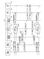
- FIG. 2 is a sequence diagram illustrating the operation of the communication apparatus 100.
- the CPU 105 has a communication selection control function 160, a communication application 170, and a built-in memory control function 180 as software functions. Therefore, in FIG. 2, the operation of the CPU 105 will be described for each of the above functions. In FIG. 2, parts having the same configuration as in FIG.
- FIG. 3 is a diagram illustrating an operating environment of the communication device 100.
- a broken line from Y ⁇ b> 1 to Y ⁇ b> 2 and a wavy line from Y ⁇ b> 2 to Y ⁇ b> 3 indicate the moving direction of the communication apparatus 100.
- the communication apparatus 100 is executing some communication application while moving from the wireless area 301 of communication A to the wireless area 302 of communication B.
- step ST201 the communication application 170 of the CPU 105 is connected to the communication A connection unit 101 (not shown in FIG. 2) and The communication data is received and operated (step ST201).
- step ST202 when executing the communication application in the communication application 170 (step ST202), the CPU 105 executes a communication control operation using the built-in memory 106 (step ST203). In addition, when executing the communication application in the communication application 170 (step ST202), the CPU 105 uses the external memory 108 to execute an application operation not related to communication control (step ST204). Note that the use of the internal memory 106 and the external memory 108 when executing the communication application will be described later.
- the communication A control unit 103 notifies the CPU 105 of a communication state notification (step ST205).
- the communication B control unit 104 notifies the CPU 105 of a communication state notification (step ST206). After receiving these notifications, the CPU 105 uses the communication selection control function 160 to grasp the radio wave conditions of the communication A and the communication B.
- the CPU 105 uses the communication selection control function 160 to determine that the communication path should be switched from the collected various information ( Step ST207).
- the CPU 105 performs communication stop control using the communication selection control function 160 for the communication A control unit 103 used so far (step ST208).
- the communication A control unit 103 blocks communication data.
- the CPU 105 notifies the built-in memory control function 180 of a request for switching the built-in memory 106 using the communication selection control function 160 (step ST209).
- the CPU 105 performs a process of writing back the control data stored in the internal memory 106 to the external memory 108 using the internal memory control function 180 (step ST210).
- the CPU 105 performs rewrite processing of the internal memory 106 by performing data transfer using the internal memory control function 180 (step ST211). This rewriting process will be described later.
- the built-in memory control function 180 notifies the CPU 105 of a built-in memory switching completion notification (step ST212).
- the CPU 105 receives a built-in memory switching completion notification using the communication selection control function 160.
- the CPU 105 performs communication start control on the communication B control unit 104 using the communication selection control function 160 (step ST213).
- communication B control section 104 receives communication data of communication B via communication B connection section 102 (not shown in FIG. 2) (step ST214). This operation is performed while the communication apparatus 100 is moving in the wireless area 302 of communication B in FIG.
- the CPU 105 uses the communication application 170 to execute the communication application while receiving communication data (step ST215). At this time, the CPU 105 executes a communication control operation using the built-in memory 106 (step ST216). Moreover, CPU105 implements application operation which is not related to communication control using the external memory 108 (step ST217).
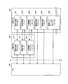
- FIG. 4 is a diagram for explaining a method of selectively using the internal memory 106 and the external memory 108 when using the communication A.
- FIG. 4 illustrates the processing of step ST202 to step ST204 in FIG.
- FIG. 4 conceptually shows an address map defined by the CPU 105, with the CPU 105, the built-in memory 106, and the external memory 108 shown side by side.
- a wavy line from X1 to X2 indicates the address traveling direction of the address map.
- the external memory 108 includes a communication A control program 401, a communication A control data 402, a common function program and data 403, a communication B control program 404, a communication B control data 405, and a communication application program and data 406. They are stored in the order shown in FIG.
- the program area of the external memory 108 is an area where the CPU 105 only performs reading.
- the data area of the external memory 108 is an area where the CPU 105 reads and rewrites data.
- the common function area of the external memory 108 is an area for storing a shared program and shared data during communication A control and communication B control.
- the communication A control program 401, the communication A control data 402, and the common function program + data 403 stored in the external memory 108 are not used. Instead, the communication A control program 411, the communication A control data 412, and the common function program + data 413 read from the external memory 108 and stored in the built-in memory 106 are used. This is for speeding up communication A by using built-in memory 106 during communication A.
- the data is written back from the built-in memory 106 to the external memory 108. At this time, the data is written back in the direction from the communication A control data 412 to the communication A control data 402 and from the common function program + data 413 to the common function program + data 403 in FIG. At this time, the program is not written back.
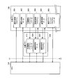
- FIG. 5 is a diagram for explaining a method of properly using the internal memory 106 and the external memory 108 when using the communication B.
- the various programs and data stored in the external memory 108 are the same as those in FIG.
- FIG. 5 conceptually shows an address map defined by the CPU 105, as in FIG. A wavy line from X1 to X2 indicates the address traveling direction of the address map.
- the built-in memory 106 stores the common function program + data 413, the communication B control data 424, and the communication B control program 425 in order to support communication B. These read out the common function program + data 403, the communication B control program 404, and the communication B control data 405 stored in the external memory 108 and stored them in the built-in memory 106, respectively.
- This storage in the built-in memory 106 is performed by data transfer to the built-in memory 106 in step ST211 of FIG.
- the common function program + data 413 can be shared by the communication A and the communication B, when the communication method to be used is switched from the communication A to the communication B, the common function program + data 413 remains stored in the built-in memory 106. , Can not be replaced.
- the common function program + data 403, the communication B control program 404, and the communication B control data 405 stored in the external memory 108 are not used. Instead, the common function program + data 413, the communication B control data 424, and the communication B control program 425 stored in the built-in memory 106 are used. This is for the purpose of speeding up the communication B by using the built-in memory 106 in the communication B as well as in the communication A.
- the area of the built-in memory 106 that stores the control data and control program for communication A, and the built-in memory 106 that stores the control data and control program for communication B are clear. It is different from the area.
- the program and data stored in the built-in memory are switched in accordance with the switching of the communication method.
- switching is performed between two types of communication methods, communication A and communication B.
- the present invention is not limited to this, and switching between any three or more types of communication methods is possible. It can be performed.
- one CPU, built-in memory, and external memory are provided.
- the present invention is not limited to this, and any number of CPUs, built-in memories, and external memories can be provided.
- the communication device and the data exchange method according to the present invention are particularly suitable for communication using a plurality of communication methods.
Landscapes
- Engineering & Computer Science (AREA)
- Computer Networks & Wireless Communication (AREA)
- Signal Processing (AREA)
- Mobile Radio Communication Systems (AREA)
- Computer And Data Communications (AREA)
Abstract
高機能化に伴う製造コストの増大及びシステム全体の通信速度の低下を抑制することができる通信装置。この通信装置(100)は、通信Aと通信Bの複数の通信方式により通信可能である。外部メモリ(108)は、各通信方式における通信を制御するために使用される制御データを通信方式毎に格納する。内蔵メモリ(106)は、外部メモリ(108)よりも高速に制御データの読み書きが可能である。CPU(105)は、使用する通信方式の制御データを外部メモリ(108)より読み出して内蔵メモリ(106)に格納することを指示するとともに、使用する通信方式を切り替える際に、内蔵メモリ(106)に格納されている切り替え前の通信方式の制御データを、外部メモリ(108)に格納されている切り替え後の通信方式の制御データに入れ替えることを指示する。
Description
本発明は、通信装置及びデータ交換方法に関し、特に複数の通信方式により通信する通信装置及びデータ交換方法に関する。
従来、通信機器における通信高速化手法として、CPUに近接する内蔵メモリを活用する実装が一般的である(例えば、特許文献1)。この手法によれば、高速化したい特定の通信制御プログラムや処理データをCPUに近接する内蔵メモリに格納し、メモリアクセスの時間ロスを最小化することで高速化を図ることができる。また、この手法は、CPUに近接する内蔵メモリを設ける点で、命令キャッシュやデータキャッシュに近い技術である。しかしながら、この手法は、設計者が用途を固定し、一般的には静的にアドレスを割り付ける点で命令キャッシュやデータキャッシュとは異なる。
また、昨今の通信機器の高機能化に応じて、無線LAN、GSM、UMTS及びLTEなどの複数の通信方式に適用可能な通信機器が一般的となりつつある。このような高機能化の通信機器では、内蔵メモリに格納するプログラムやデータは、対応する通信方式の数に応じて増加する。
しかしながら、従来の機器においては、内蔵メモリはCPUと同じLSIに搭載されるため、内蔵メモリに格納するプログラムやデータの増加に伴って、LSIの製造コストが増大するという問題がある。また、従来の機器においては、内蔵メモリに格納するプログラムやデータの増加に伴って内蔵メモリの容量が増加し、システム全体の通信速度の低下を招くという問題がある。
本発明の目的は、高機能化に伴う製造コストの増大及びシステム全体の通信速度の低下を抑制することができる通信装置及びデータ交換方法を提供することである。
本発明の通信装置は、複数の通信方式により通信可能な通信装置であって、各通信方式における通信を制御するために使用される制御データを通信方式毎に格納する第1の格納手段と、前記第1の格納手段よりも高速に前記制御データの読み書きが可能な第2の格納手段と、使用する通信方式の前記制御データを前記第1の格納手段より読み出して前記第2の格納手段に格納するとともに、使用する通信方式を切り替える際に、前記第2の格納手段に格納されている切り替え前の通信方式の前記制御データを、前記第1の格納手段に格納されている切り替え後の通信方式の前記制御データに入れ替える制御手段と、前記第2の格納手段に格納した前記制御データにより制御可能な通信方式で通信を行う通信手段と、を具備する構成を採る。
本発明のデータ交換方法は、複数の通信方式により通信可能な通信装置におけるデータ交換方法であって、各通信方式における通信を制御するために使用される制御データを通信方式毎に格納する第1の格納手段より、使用する通信方式の前記制御データを読み出すステップと、前記第1の格納手段よりも高速に前記制御データの読み書きが可能な第2の格納手段に、前記第1の格納手段から読み出した前記制御データを格納するステップと、使用する通信方式を切り替える際に、前記第2の格納手段に記憶する切り替え前の通信方式の前記制御データを、前記第1の格納手段に記憶する切り替え後の通信方式の前記制御データに入れ替えるステップと、を具備するようにした。
本発明によれば、高機能化に伴う製造コストの増大及びシステム全体の通信速度の低下を抑制することができる。
以下、本発明の実施の形態について、図面を参照して詳細に説明する。
(実施の形態)
図1は、本発明の実施の形態に係る通信装置100の構成を示すブロック図である。通信装置100は、例えば携帯電話等の通信端末装置である。なお、図1では、2種類の通信方式(通信A及び通信B)に対応する通信装置100について説明する。
図1は、本発明の実施の形態に係る通信装置100の構成を示すブロック図である。通信装置100は、例えば携帯電話等の通信端末装置である。なお、図1では、2種類の通信方式(通信A及び通信B)に対応する通信装置100について説明する。
図1では、LSI150は、通信A制御部103と、通信B制御部104と、CPU105と、内蔵メモリ106と、外部メモリ制御部107とを含む。
通信A接続部101は、通信A制御部103の制御に従って、通信Aの通信方式により通信相手と接続して通信を行う。
通信B接続部102は、通信B制御部104の制御に従って、通信Bの通信方式により通信相手と接続して通信を行う。
通信A制御部103は、CPU105の指示に従って、通信A接続部101の制御を行う。具体的には、通信A制御部103は、内蔵メモリ106に格納されている通信Aのデータまたはプログラムを使用して、通信Aにおける通信を制御する。ここで、通信Aのデータ及びプログラムには、通信Aの制御データ及び通信Aの制御プログラムに加えて、通信Aと通信Bとで共用する共通機能データ及び共通機能プログラムを含む。また、通信Aの制御データは、通信Aによる通信を制御するために使用される。
通信B制御部104は、CPU105の指示に従って、通信B接続部102の制御を行う。具体的には、通信B制御部104は、内蔵メモリ106に格納されている通信Bのデータまたはプログラムを使用して、通信Bにおける通信を制御する。ここで、通信Bのデータ及びプログラムには、通信Bの制御データ及び通信Bの制御プログラムに加えて、通信Aと通信Bとで共用する共通機能データ及び共通機能プログラムを含む。また、通信Bの制御データは、通信Bによる通信を制御するために使用される。
CPU105は、通信A制御部103に対して、通信A接続部101を制御することを指示する。また、CPU105は、通信B制御部104に対して、通信B接続部102を制御することを指示する。また、CPU105は、外部メモリ制御部107に対して、外部メモリ108へのデータ若しくはプログラムの格納、または外部メモリ108からのデータ若しくはプログラムの読み出しを指示する。
具体的には、CPU105は、使用する通信方式のデータまたはプログラムを外部メモリ108から読み出すことを外部メモリ制御部107に指示する。また、CPU105は、使用する通信方式を切り替える際に、切り替え前の通信方式のデータを内蔵メモリ106から読み出して外部メモリ108に格納することを、外部メモリ制御部107に指示する。また、CPU105は、使用する通信方式を切り替える際に、切り替え後の通信方式のデータを外部メモリ108から読み出して内蔵メモリ106へ格納することを、外部メモリ制御部107に指示する。即ち、CPU105は、使用する通信方式を切り替える際に、内蔵メモリ106に格納するデータを入れ替えるとともに、内蔵メモリ106と外部メモリ108との間でデータ交換する制御を行う。
内蔵メモリ106は、CPU105に近接するメモリであり、外部メモリ制御部107により外部メモリ108から読み出されたデータまたはプログラムを格納する。また、内蔵メモリ106は、外部メモリ108よりも高速にデータまたはプログラムを読み書きすることができる。
外部メモリ制御部107は、CPU105の指示に従って、外部メモリ108に格納されているデータまたはプログラムを外部メモリ108から読み出して内蔵メモリ106に格納する。また、外部メモリ制御部107は、CPU105の指示に従って、内蔵メモリ106に格納されているデータを外部メモリ108に格納する。これにより、外部メモリ108に格納されているデータが更新される。
外部メモリ108は、LSI150の外部に接続されたメモリであり、通信A及び通信Bで使用するデータ及びプログラムを通信方式毎に格納する。
次に、通信装置100の動作について、図2を用いて説明する。図2は、通信装置100の動作を示すシーケンス図である。
CPU105は、ソフトウェア機能として、通信選択制御機能160と、通信アプリケーション170と、内蔵メモリ制御機能180とを有する。従って、図2では、CPU105については、上記の機能毎に動作を説明する。なお、図2において、図1と同一構成である部分には同一の符号を付している。
また、図2では、図3に示すような移動通信を想定する。図3は、通信装置100の動作環境を示す図である。図3において、Y1からY2に至る破線、及びY2からY3に至る波線は、通信装置100の移動方向を示している。以下においては、通信装置100が、通信Aの無線領域301から、通信Bの無線領域302に移動しながら、何らかの通信アプリケーションを実施している状況を想定して説明する。
図2より、まず、通信装置100が図3に示す通信Aの無線領域301に居る期間は、CPU105の通信アプリケーション170は、通信A接続部101(図2において図示省略)及び通信A制御部103を介して通信データを受信して動作する(ステップST201)。
次に、CPU105は、通信アプリケーション170における通信アプリケーション実行の際に(ステップST202)、内蔵メモリ106を用いて通信制御動作を実行する(ステップST203)。また、CPU105は、通信アプリケーション170における通信アプリケーション実行の際に(ステップST202)、外部メモリ108を用いて、通信制御に関係しないアプリケーション動作を実施する(ステップST204)。なお、通信アプリケーション実行の際における、内蔵メモリ106と外部メモリ108との使い分けについては後述する。
また、通信A制御部103は、通信状態通知をCPU105に通知する(ステップST205)。
また、通信B制御部104は、通信状態通知をCPU105に通知する(ステップST206)。CPU105は、これらの通知を受けた後、通信選択制御機能160を用いて通信A及び通信Bの電波状態等を把握する。
CPU105は、通信装置100が移動を継続して図3に示すY2の位置に到達した際に、通信選択制御機能160を用いて、収集した各種情報から通信路を切り替えるべきとの判断を行う(ステップST207)。
次に、CPU105は、これまで使用していた通信A制御部103に対して、通信選択制御機能160を用いて通信停止制御を行う(ステップST208)。これにより、通信A制御部103は、通信データを遮断する。
また、CPU105は、通信選択制御機能160を用いて、内蔵メモリ制御機能180に対して、内蔵メモリ106の切り替え要求を通知する(ステップST209)。
次に、CPU105は、内蔵メモリ制御機能180を用いて、内蔵メモリ106に格納されている制御データを外部メモリ108に書き戻す処理を行う(ステップST210)。
次に、CPU105は、内蔵メモリ制御機能180を用いてデータ転送を行うことにより、内蔵メモリ106の書き換え処理を行う(ステップST211)。なお、この書き換え処理については後述する。
また、内蔵メモリ制御機能180は、ステップST211におけるデータ転送が完了した後、内蔵メモリ切り替え完了通知をCPU105に通知する(ステップST212)。また、CPU105は、通信選択制御機能160を用いて、内蔵メモリ切り替え完了通知を受け取る。
次に、CPU105は、通信選択制御機能160を用いて、通信B制御部104に対して通信開始制御を行う(ステップST213)。
次に、通信B制御部104は、通信B接続部102(図2において図示省略)を介して通信Bの通信データを受信する(ステップST214)。この動作は、通信装置100が図3の通信Bの無線領域302を移動中に行う。
また、CPU105は、通信アプリケーション170を用いて、通信データを受信しながら通信アプリケーションの実行を行う(ステップST215)。この際に、CPU105は、内蔵メモリ106を用いて通信制御動作を実行する(ステップST216)。また、CPU105は、外部メモリ108を用いて、通信制御に関係しないアプリケーション動作を実施する(ステップST217)。
次に、通信Aを使用する場合における内蔵メモリ106及び外部メモリ108の使い分けについて、図4を用いて説明する。図4は、通信Aを使用する場合における内蔵メモリ106及び外部メモリ108を使い分ける方法を説明する図である。なお、図4は、図2のステップST202~ステップST204の処理を説明するものである。
図4は、CPU105と、内蔵メモリ106と、外部メモリ108とを横並びに記載し、CPU105が定義するアドレスマップを概念的に示したものである。また、図4において、X1からX2に至る波線は、アドレスマップのアドレス進行方向を示す。
外部メモリ108には、通信A制御プログラム401と、通信A制御データ402と、共通機能プログラム及びデータ403と、通信B制御プログラム404と、通信B制御データ405と、通信アプリケーションプログラム及びデータ406とが図4に示す順序で格納されている。
また、外部メモリ108のプログラム領域は、CPU105が読み出しのみを行う領域である。また、外部メモリ108のデータ領域は、CPU105が読み出し及び書き換えを行う領域である。また、外部メモリ108の共通機能領域は、通信A制御時と通信B制御時とで、共用するプログラム及び共用するデータを格納する領域である。
図2のステップST202の通信アプリケーション実行では、外部メモリ108に格納されている通信A制御プログラム401と、通信A制御データ402と、共通機能プログラム+データ403とは使用しない。その代わりに、外部メモリ108から読み出されて内蔵メモリ106に格納された通信A制御プログラム411と、通信A制御データ412と、共通機能プログラム+データ413とが使用される。これは、通信Aでの通信時に内蔵メモリ106を使用することにより、通信Aの高速化を図るためである。
また、図2のステップST210の外部メモリ108へのデータ転送では、内蔵メモリ106から外部メモリ108にデータを書き戻す。この際、データを書き戻す方向は、図4において、通信A制御データ412から通信A制御データ402に向かう方向、及び共通機能プログラム+データ413から共通機能プログラム+データ403に向かう方向である。また、この際、プログラムの書き戻しは行わない。
次に、通信Bを使用する場合における内蔵メモリ106及び外部メモリ108の使い分けについて、図5を用いて説明する。図5は、通信Bを使用する場合における内蔵メモリ106及び外部メモリ108を使い分ける方法を説明する図である。なお、外部メモリ108に格納されている各種プログラム及びデータは、図4と同一であるので、その説明を省略する。
図5は図4と同様に、CPU105が定義するアドレスマップを概念的に示したものである。また、X1からX2に至る波線は、アドレスマップのアドレス進行方向を示す。
図5が図4と異なる点は、内蔵メモリ106のアドレスマップ上の配置である。即ち、図5では、内蔵メモリ106は、通信Bに対応するために、共通機能プログラム+データ413と、通信B制御データ424と、通信B制御プログラム425とを格納する。これらは、外部メモリ108に格納される共通機能プログラム+データ403と、通信B制御プログラム404と、通信B制御データ405とを読み出して、それぞれ内蔵メモリ106に格納したものである。この内蔵メモリ106への格納は、図2のステップST211の内蔵メモリ106へのデータ転送により実施される。
ただし、共通機能プログラム+データ413は、通信Aと通信Bとで共用可能であるため、使用する通信方式を通信Aから通信Bに切り替える際には、内蔵メモリ106に格納したままの状態であり、入れ替えられない。
また、図2のステップST215の通信アプリケーション実行では、外部メモリ108に格納される共通機能プログラム+データ403と、通信B制御プログラム404と、通信B制御データ405とは使用しない。その代わりに、内蔵メモリ106に格納された共通機能プログラム+データ413と、通信B制御データ424と、通信B制御プログラム425とを使用する。これは、通信Aでの通信時と同様に、通信Bでの通信時においても、内蔵メモリ106を使用することにより、通信Bの高速化を図るためである。
また、図4と図5とを比較することにより明らかなように、通信Aの制御データ及び制御プログラムを格納する内蔵メモリ106の領域と、通信Bの制御データ及び制御プログラムを格納する内蔵メモリ106の領域とは異なる。
このように、本実施の形態では、通信方式の切り替えに応じて、内蔵メモリに格納するプログラム及びデータを入れ替える。これにより、本実施の形態によれば、高機能化に伴う製造コストの増大及びシステム全体の速度低下を抑制することができるとともに、CPUの負荷の低減を図ることができる。
なお、本実施の形態において、通信Aと通信Bの2種類の通信方式の間で切り替えを行ったが、本発明はこれに限らず、3種類以上の任意の種類の通信方式の間で切り替えを行うことができる。
また、本実施の形態において、CPU、内蔵メモリ及び外部メモリを1つずつ設けたが、本発明はこれに限らず、CPU、内蔵メモリ及び外部メモリの各々を任意の数だけ設けることができる。
また、内蔵メモリ及び外部メモリのアドレスについては、本実施の形態以外の割り付け方法も可能である。
2011年3月9日出願の特願2011-51613の日本出願に含まれる明細書、図面及び要約書の開示内容は、すべて本願に援用される。
本発明にかかる通信装置及びデータ交換方法は、特に複数の通信方式により通信するのに好適である。
100 通信装置
101 通信A接続部
102 通信B接続部
103 通信A制御部
104 通信B制御部
105 CPU
106 内蔵メモリ
107 外部メモリ制御部
108 外部メモリ
101 通信A接続部
102 通信B接続部
103 通信A制御部
104 通信B制御部
105 CPU
106 内蔵メモリ
107 外部メモリ制御部
108 外部メモリ
Claims (5)
- 複数の通信方式により通信可能な通信装置であって、
各通信方式における通信を制御するために使用される制御データを通信方式毎に格納する第1の格納手段と、
前記第1の格納手段よりも高速に前記制御データの読み書きが可能な第2の格納手段と、
使用する通信方式の前記制御データを前記第1の格納手段より読み出して前記第2の格納手段に格納するとともに、使用する通信方式を切り替える際に、前記第2の格納手段に格納されている切り替え前の通信方式の前記制御データを、前記第1の格納手段に格納されている切り替え後の通信方式の前記制御データに入れ替える制御手段と、
前記第2の格納手段に格納した前記制御データにより制御可能な通信方式で通信を行う通信手段と、
を具備する通信装置。 - 前記第1の格納手段は、前記制御データに加えて、複数の通信方式において共用する共通機能データを格納し、
前記制御手段は、使用する通信方式の前記共通機能データを前記第1の格納手段より読み出して前記第2の格納手段に格納するとともに、使用する通信方式を切り替える際に、切り替え前後の通信方式で共用する前記共通機能データの入れ替えを行わない請求項1記載の通信装置。 - 前記制御手段は、使用する通信方式を切り替える際に、前記第1の格納手段に格納されている切り替え前の通信方式の前記制御データを、前記第2の格納手段に格納されている切り替え前の通信方式の前記制御データに更新する請求項1記載の通信装置。
- 前記制御手段は、前記切り替え前の通信方式の前記制御データを格納する前記第2の格納手段の格納領域と異なる格納領域に、前記切り替え後の通信方式の前記制御データを格納する請求項1記載の通信装置。
- 複数の通信方式により通信可能な通信装置におけるデータ交換方法であって、
各通信方式における通信を制御するために使用される制御データを通信方式毎に格納する第1の格納手段より、使用する通信方式の前記制御データを読み出すステップと、
前記第1の格納手段よりも高速に前記制御データの読み書きが可能な第2の格納手段に、前記第1の格納手段から読み出した前記制御データを格納するステップと、
使用する通信方式を切り替える際に、前記第2の格納手段に記憶する切り替え前の通信方式の前記制御データを、前記第1の格納手段に記憶する切り替え後の通信方式の前記制御データに入れ替えるステップと、
を具備するデータ交換方法。
Priority Applications (1)
| Application Number | Priority Date | Filing Date | Title |
|---|---|---|---|
| US14/002,278 US20130337865A1 (en) | 2011-03-09 | 2012-03-09 | Communication device and data exchange method |
Applications Claiming Priority (2)
| Application Number | Priority Date | Filing Date | Title |
|---|---|---|---|
| JP2011051613A JP2012190143A (ja) | 2011-03-09 | 2011-03-09 | 通信装置及びデータ交換方法 |
| JP2011-051613 | 2011-03-09 |
Publications (1)
| Publication Number | Publication Date |
|---|---|
| WO2012120898A1 true WO2012120898A1 (ja) | 2012-09-13 |
Family
ID=46797869
Family Applications (1)
| Application Number | Title | Priority Date | Filing Date |
|---|---|---|---|
| PCT/JP2012/001643 Ceased WO2012120898A1 (ja) | 2011-03-09 | 2012-03-09 | 通信装置及びデータ交換方法 |
Country Status (3)
| Country | Link |
|---|---|
| US (1) | US20130337865A1 (ja) |
| JP (1) | JP2012190143A (ja) |
| WO (1) | WO2012120898A1 (ja) |
Citations (4)
| Publication number | Priority date | Publication date | Assignee | Title |
|---|---|---|---|---|
| JP2000286917A (ja) * | 1999-03-30 | 2000-10-13 | Kokusai Electric Co Ltd | 通信処理装置 |
| JP2003244159A (ja) * | 2002-02-21 | 2003-08-29 | Seiko Epson Corp | 無線通信における通信チャンネルの切り換え制御 |
| JP2003283651A (ja) * | 2002-03-22 | 2003-10-03 | Toshiba Corp | 携帯無線通信装置 |
| JP2008146486A (ja) * | 2006-12-12 | 2008-06-26 | Canon Inc | 通信装置、通信装置の制御方法及びプログラム |
Family Cites Families (2)
| Publication number | Priority date | Publication date | Assignee | Title |
|---|---|---|---|---|
| JP4930553B2 (ja) * | 2009-06-30 | 2012-05-16 | 富士通株式会社 | データ移行機能を有した装置及びデータ移行方法 |
| JP5849400B2 (ja) * | 2011-02-08 | 2016-01-27 | コニカミノルタ株式会社 | 画像形成方法および画像形成装置 |
-
2011
- 2011-03-09 JP JP2011051613A patent/JP2012190143A/ja not_active Withdrawn
-
2012
- 2012-03-09 US US14/002,278 patent/US20130337865A1/en not_active Abandoned
- 2012-03-09 WO PCT/JP2012/001643 patent/WO2012120898A1/ja not_active Ceased
Patent Citations (4)
| Publication number | Priority date | Publication date | Assignee | Title |
|---|---|---|---|---|
| JP2000286917A (ja) * | 1999-03-30 | 2000-10-13 | Kokusai Electric Co Ltd | 通信処理装置 |
| JP2003244159A (ja) * | 2002-02-21 | 2003-08-29 | Seiko Epson Corp | 無線通信における通信チャンネルの切り換え制御 |
| JP2003283651A (ja) * | 2002-03-22 | 2003-10-03 | Toshiba Corp | 携帯無線通信装置 |
| JP2008146486A (ja) * | 2006-12-12 | 2008-06-26 | Canon Inc | 通信装置、通信装置の制御方法及びプログラム |
Also Published As
| Publication number | Publication date |
|---|---|
| JP2012190143A (ja) | 2012-10-04 |
| US20130337865A1 (en) | 2013-12-19 |
Similar Documents
| Publication | Publication Date | Title |
|---|---|---|
| US7062616B2 (en) | Implementing a dual partition flash with suspend/resume capabilities | |
| JP6744806B2 (ja) | マルチプロセッサ | |
| CN101876925B (zh) | 内存镜像处理方法、装置和系统 | |
| JP2009003768A (ja) | メモリ共有システム装置 | |
| US20140132979A1 (en) | Information processing apparatus, information processing method, and storage medium | |
| US8832407B2 (en) | Communication device with storage function | |
| CN107544937A (zh) | 一种协处理器、数据写入方法和处理器 | |
| US12299285B2 (en) | Compressed memory buffer device | |
| US9934100B2 (en) | Method of controlling memory swap operation and data processing system using same | |
| JP4632099B2 (ja) | メモリ制御装置及びその制御方法 | |
| US20140281053A1 (en) | I/o device control system and method for controlling i/o device | |
| JP2009020555A (ja) | スワップ処理装置 | |
| JP5209535B2 (ja) | Usbホストコントローラ及びusbホストコントローラの制御方法 | |
| WO2012120898A1 (ja) | 通信装置及びデータ交換方法 | |
| CN107071714A (zh) | 一种移动终端及其蓝牙加载控制方法、及存储装置 | |
| KR102076248B1 (ko) | 선택 지연 가비지 컬렉션 방법 및 이를 이용한 메모리 시스템 | |
| CN105824575A (zh) | 具有编程状态的存储器系统与存储器控制方法 | |
| WO2023240941A1 (zh) | 下载数据的方法、装置和安全元件 | |
| CN104298616B (zh) | 数据块初始化方法、高速缓冲存储器和终端 | |
| JP5231496B2 (ja) | 情報処理装置及びそのサスペンド/リジューム方法 | |
| JP4689052B2 (ja) | 携帯通信端末 | |
| JP4841192B2 (ja) | 信号処理回路および方法、並びに情報処理装置 | |
| JP5967054B2 (ja) | ストレージ装置、コントローラ、ストレージシステム、データアクセス方法およびプログラム | |
| JP4038520B2 (ja) | サービス制御装置及びサービス制御方法 | |
| JP2008217659A (ja) | Dma転送起動方法 |
Legal Events
| Date | Code | Title | Description |
|---|---|---|---|
| 121 | Ep: the epo has been informed by wipo that ep was designated in this application |
Ref document number: 12755535 Country of ref document: EP Kind code of ref document: A1 |
|
| WWE | Wipo information: entry into national phase |
Ref document number: 14002278 Country of ref document: US |
|
| NENP | Non-entry into the national phase |
Ref country code: DE |
|
| 122 | Ep: pct application non-entry in european phase |
Ref document number: 12755535 Country of ref document: EP Kind code of ref document: A1 |