WO2012118114A1 - 裏面電極型太陽電池セル、裏面電極型太陽電池サブセルおよび太陽電池モジュール - Google Patents
裏面電極型太陽電池セル、裏面電極型太陽電池サブセルおよび太陽電池モジュール Download PDFInfo
- Publication number
- WO2012118114A1 WO2012118114A1 PCT/JP2012/055060 JP2012055060W WO2012118114A1 WO 2012118114 A1 WO2012118114 A1 WO 2012118114A1 JP 2012055060 W JP2012055060 W JP 2012055060W WO 2012118114 A1 WO2012118114 A1 WO 2012118114A1
- Authority
- WO
- WIPO (PCT)
- Prior art keywords
- solar cell
- electrode
- mark
- subcell
- back electrode
- Prior art date
- Legal status (The legal status is an assumption and is not a legal conclusion. Google has not performed a legal analysis and makes no representation as to the accuracy of the status listed.)
- Ceased
Links
Images







Classifications
-
- H—ELECTRICITY
- H10—SEMICONDUCTOR DEVICES; ELECTRIC SOLID-STATE DEVICES NOT OTHERWISE PROVIDED FOR
- H10F—INORGANIC SEMICONDUCTOR DEVICES SENSITIVE TO INFRARED RADIATION, LIGHT, ELECTROMAGNETIC RADIATION OF SHORTER WAVELENGTH OR CORPUSCULAR RADIATION
- H10F19/00—Integrated devices, or assemblies of multiple devices, comprising at least one photovoltaic cell covered by group H10F10/00, e.g. photovoltaic modules
- H10F19/90—Structures for connecting between photovoltaic cells, e.g. interconnections or insulating spacers
- H10F19/902—Structures for connecting between photovoltaic cells, e.g. interconnections or insulating spacers for series or parallel connection of photovoltaic cells
- H10F19/908—Structures for connecting between photovoltaic cells, e.g. interconnections or insulating spacers for series or parallel connection of photovoltaic cells for back-contact photovoltaic cells
-
- H—ELECTRICITY
- H10—SEMICONDUCTOR DEVICES; ELECTRIC SOLID-STATE DEVICES NOT OTHERWISE PROVIDED FOR
- H10F—INORGANIC SEMICONDUCTOR DEVICES SENSITIVE TO INFRARED RADIATION, LIGHT, ELECTROMAGNETIC RADIATION OF SHORTER WAVELENGTH OR CORPUSCULAR RADIATION
- H10F77/00—Constructional details of devices covered by this subclass
- H10F77/20—Electrodes
- H10F77/206—Electrodes for devices having potential barriers
- H10F77/211—Electrodes for devices having potential barriers for photovoltaic cells
- H10F77/219—Arrangements for electrodes of back-contact photovoltaic cells
-
- Y—GENERAL TAGGING OF NEW TECHNOLOGICAL DEVELOPMENTS; GENERAL TAGGING OF CROSS-SECTIONAL TECHNOLOGIES SPANNING OVER SEVERAL SECTIONS OF THE IPC; TECHNICAL SUBJECTS COVERED BY FORMER USPC CROSS-REFERENCE ART COLLECTIONS [XRACs] AND DIGESTS
- Y02—TECHNOLOGIES OR APPLICATIONS FOR MITIGATION OR ADAPTATION AGAINST CLIMATE CHANGE
- Y02E—REDUCTION OF GREENHOUSE GAS [GHG] EMISSIONS, RELATED TO ENERGY GENERATION, TRANSMISSION OR DISTRIBUTION
- Y02E10/00—Energy generation through renewable energy sources
- Y02E10/50—Photovoltaic [PV] energy
Definitions
- the present invention relates to a back electrode type solar cell, a back electrode type solar cell subcell, and a solar cell module, and in particular, a back electrode type in which an n electrode and a p electrode are provided on a back surface opposite to a light receiving surface.
- the present invention relates to a solar battery cell, a back electrode type solar battery subcell, and a solar battery module.
- Patent Document 1 discloses a solar cell module that includes a plurality of solar cell wafers (back electrode type solar cells) and a wiring board that electrically connects the plurality of solar cell wafers.
- the size of the solar cell module may not be determined from the size of the solar cell wafer.
- Patent Document 2 discloses a solar cell module in which the effective area ratio is increased by arranging trapezoidal solar cell elements (solar cell subcells) and pentagonal solar cell elements in combination. This trapezoidal solar cell element and pentagonal solar cell element are obtained by dividing a hexagonal solar cell into two at different positions.
- electrodes having different polarities are provided on the light receiving surface and the back surface of the solar cell element. And the electrode of the light-receiving surface side of a solar cell element is electrically connected to the electrode of the back surface side of an adjacent solar cell element using a connection line.
- an electrode is provided on the light receiving surface of the solar cell element, and the connection line connected to the electrode is also disposed on the light receiving surface of the solar cell element. Since light does not enter the region of the light receiving surface of the solar cell element to be arranged and power is not generated, the power generation efficiency of the solar cell element cannot be improved. Moreover, when electrically connecting adjacent solar cell elements (solar cell subcell), it is necessary to attach a connection line to both the light-receiving surface side and the back surface side. For this reason, there exists a problem that manufacture of a solar cell module takes time.
- the present invention has been made to solve the above-described problems, and an object of the present invention is to reduce the manufacturing time of the solar cell module and to generate power while suppressing an increase in the types of solar cell subcells. It is to provide a back electrode type solar cell, a back electrode type solar cell and a solar cell module capable of realizing an improvement in efficiency.
- a back electrode type solar cell of the present invention is provided with a light receiving surface for receiving light, a back surface disposed on the side opposite to the light receiving surface, a back surface side, and a first direction.
- N electrode and p electrode arranged alternately, and the arrangement pattern of the n electrode is symmetric about a predetermined point located at the center of the back surface, and the arrangement pattern of the p electrode has a predetermined point The center is point-symmetric, and the n-electrode and the p-electrode are arranged at a predetermined distance from a straight line that passes through a predetermined point and extends in the first direction.
- the “center portion of the back surface” refers to a range of a distance corresponding to the interelectrode pitch between the n electrode and the p electrode from the center point of the back surface.
- the electrode arrangement pattern is point-symmetric is obtained not only when the electrode shape (length, width, etc.) is completely point-symmetric but also by dividing the back electrode type solar cell. It also includes an electrode arrangement pattern that can be mounted on the same wiring board (wiring pattern) when the back electrode type solar cell subcell is rotated 180 degrees.
- this back electrode type solar cell it is possible to suppress the reduction of the light receiving area by providing the n electrode and the p electrode on the back surface side as described above. Moreover, when electrically connecting adjacent back surface electrode type solar cell subcells, wiring is possible only on the back surface side.
- the arrangement pattern of the n electrode is point symmetric about a predetermined point
- the arrangement pattern of the p electrode is point symmetric about a predetermined point, so that the first electrode passes through the predetermined point.
- the arrangement pattern of the electrodes of the back electrode type solar cell sub-cells obtained by dividing the back electrode type solar cell by the straight line extending in the direction is the same (or common).
- the n electrode and the p electrode are arranged at a predetermined distance from a straight line that passes through a predetermined point and extends in the first direction.
- the first part is formed in a shape that is not line symmetric with respect to an axis extending in the first direction
- the second portion is formed in a shape that is not line symmetric with respect to an axis extending in the first direction.
- the predetermined point is a center point of the back surface.
- the back electrode solar cell preferably includes a first part and a second part separated by the straight line, the first part is provided with a first mark, and the second part is provided with a second mark.
- the first mark and the second mark are arranged at positions that are symmetric with respect to each other about a predetermined point. In this case, if the first mark and the second mark are used as alignment marks for alignment when mounting the divided back electrode type solar cell subcell (first portion and second portion) on the wiring board, the back electrode type The solar battery subcell (the first portion and the second portion) can be easily mounted on the wiring board.
- the first mark and the second mark are formed in different shapes. Yes. If comprised in this way, it can identify easily whether the back surface electrode type solar cell subcell after a division
- segmentation is a 1st part or a 2nd part from the shape of a mark (a 1st mark and a 2nd mark). it can.
- each of the first mark and the second mark is provided in plural.
- At least one of the first mark and at least one of the second mark are disposed on an extension of one of the n-electrode and the p-electrode, and at least one of the remaining first mark and at least one of the second mark. Is arranged on the other extension line of the n-electrode and the p-electrode.
- the back electrode type solar cell of the present invention is formed by dividing the back electrode type solar cell having the above-described configuration at the position of the straight line.
- a solar cell module of the present invention includes a plurality of back electrode type solar cell subcells having the above-described configuration, and a wiring board on which the plurality of back electrode type solar cell subcells are mounted. It arrange
- an odd number of back electrode type solar cell subcells are arranged on the wiring board in a second direction orthogonal to the first direction.
- the wiring substrate has a first back electrode type solar cell and a second back electrode type solar cell obtained by dividing the back electrode type solar cell at the position of the straight line. Only one of the battery subcells is mounted.
- the arrangement pattern of the n electrode is point symmetric about a predetermined point
- the arrangement pattern of the p electrode is point symmetric about a predetermined point, so that it is a straight line passing through the predetermined point.
- the arrangement pattern of the electrodes of the back electrode type solar cell subcell obtained by dividing the back electrode type solar cell is the same (or common). That is, a plurality of back electrode type solar cell subcells obtained when the back electrode type solar cell is divided can be handled as one type of back electrode type solar cell subcell. Thereby, the manufacturing process of the solar cell module can be further simplified, and the manufacturing time can be further shortened. Moreover, if such a back electrode type solar cell subcell is arranged in the same direction to constitute a solar cell module, the arrangement of the back electrode type solar cell subcells can have a sense of unity, and the design characteristics of the solar cell module Can be improved.
- a back electrode type is formed in a direction (second direction) orthogonal to the first direction.
- second direction an odd number of solar cell subcells may be arranged. That is, the back electrode type solar cell subcells can be spread in the second direction in half the size of the back electrode type solar cell.
- the n electrode and the p electrode are arranged at a predetermined distance from a straight line that passes through a predetermined point and extends in the first direction.
- a solar cell module 1 includes a plurality of (for example, three) back electrode type solar cell subcells (hereinafter simply referred to as solar cell subcells) 2 and a plurality of solar cells.
- a wiring substrate 3 on which the subcell 2 is mounted, a sealing material 4 that covers the surface of the solar cell subcell 2, and a transparent substrate 5 disposed on the sealing material 4 are provided.
- the solar cell module 1 may include a sealing material that covers the back surface side of the wiring substrate 3 and a back film (not shown).
- the solar cell module 1 may include a frame body (not shown) that fixes the peripheral portions of the wiring substrate 3 and the transparent substrate 5, and may be formed integrally with the roofing material.
- the solar cell subcell 2 is formed in a shape in which, for example, two rectangular corner portions are cut out.
- the length of the long side direction (B direction) of the solar cell subcell 2 is about 156 mm
- the length of the short side direction (A direction) is about 78 mm.
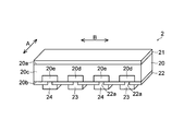
- the solar cell subcell 2 and the back electrode type solar cell 10 to be described later include a semiconductor substrate 20, an antireflection film 21 provided on the light receiving surface 20a of the semiconductor substrate 20, and a semiconductor. It includes a passivation layer 22, an n-electrode 23, and a p-electrode 24 provided on the back surface (surface opposite to the light receiving surface 20a) 20b of the substrate 20.
- the semiconductor substrate 20 is formed using, for example, an n-type single crystal silicon substrate.
- the semiconductor substrate 20 is provided on the n-type conductive region 20c, the back surface 20b side of the semiconductor substrate 20, and has an n-type diffusion region 20d having an n-type impurity at a concentration higher than that of the n-type conductive region 20c.
- a p-type diffusion region 20e having a p-type impurity provided on the back surface 20b side.
- Each of the n-type diffusion region 20d and the p-type diffusion region 20e is formed in a strip shape extending in the short side direction (A direction (second direction)) of the solar cell subcell 2, for example.
- the n-type diffusion regions 20d and the p-type diffusion regions 20e are alternately arranged in the B direction (first direction) orthogonal to the A direction.
- B direction first direction
- two n-type diffusion regions 20d and two p-type diffusion regions 20e are shown.
- a large number (for example, several tens or more) of n-type diffusion regions 20d and p-type diffusion regions 20e may be arranged. Good.
- the n-electrode 23 is in ohmic contact with the n-type diffusion region 20 d through the opening 22 a of the passivation layer 22.
- the p-electrode 24 is in ohmic contact with the p-type diffusion region 20 e through the opening 22 a of the passivation layer 22.
- each of the n electrode 23 and the p electrode 24 is formed in a strip shape extending in the A direction, for example, as shown in FIG.
- the n electrodes 23 and the p electrodes 24 are alternately arranged in the B direction.
- the interelectrode pitch between the n electrode 23 and the p electrode 24 is, for example, 750 ⁇ m.
- the number of wirings of the n electrode 23, the p electrode 24, and the wiring board 3 is reduced in order to facilitate understanding.
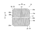
- the solar cell subcell 2 is shown in FIG. 6 as a back electrode type solar cell (hereinafter simply referred to as a solar cell) 10 having a shape in which, for example, four square corner portions shown in FIG. 5 are cut out. Thus, it is obtained by dividing (cutting) into two.
- a two-dot chain line (straight line L ⁇ b> 1) in FIG. 5 indicates a division position when dividing the solar battery cell 10.
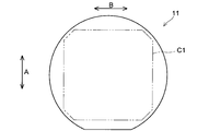
- the solar battery cell 10 uses, for example, a general wafer manufacturing process after dividing (cutting) the substantially circular semiconductor wafer 11 shown in FIG. 7 at the dividing position C1 (two-dot chain line in FIG. 7).
- a general wafer manufacturing process after dividing (cutting) the substantially circular semiconductor wafer 11 shown in FIG. 7 at the dividing position C1 (two-dot chain line in FIG. 7).
- an n-type diffusion region 20d, a p-type diffusion region 20e, an antireflection film 21, a passivation layer 22, an n electrode 23, a p electrode 24, and marks 25a and 25b are formed.
- the n-electrode 23 (arrangement pattern of the n-electrode 23) is formed point-symmetrically (180-degree rotationally symmetric) about the center point O ⁇ b> 1 of the back surface 20 b of the solar battery cell 10.
- the p-electrode 24 (arrangement pattern of the p-electrode 24) and the marks 25a and 25b are formed symmetrically with respect to the center point O1.
- the solar cell 10 when the solar cell 10 is divided into two parts 10a and 10b (first part and second part) by a straight line L1 passing through the center point O1 and extending in the B direction, the n electrode 23, the p electrode 24, The marks 25a and 25b (first mark), the n electrode 23, the p electrode 24, and the marks 25a and 25b (second mark) of the portion 10b are formed point-symmetrically with respect to the center point O1. Further, the outer shape of the solar battery cell 10 (parts 10a and 10b) is also formed substantially symmetrical with respect to the center point O1.
- solar cell subcells 2 a and 2 b obtained by dividing solar cell 10 have the same shape (outer shape, electrode arrangement pattern) as the other when one cell is rotated 180 degrees.
- Solar cell subcells 2a and 2b correspond to portions 10a and 10b of solar cell 10, respectively.
- Each of solar cell subcells 2a and 2b is formed in a shape that is not line-symmetric with respect to an axis (not shown) extending in the B direction, for example.
- the mark 25a and the mark 25b may be formed in different shapes.
- the mark 25a is formed in a circle (perfect circle) shape
- the mark 25b is formed in a square shape.
- the marks 25a and 25b may be used as alignment marks for alignment when the solar cell subcell 2 is mounted on the wiring board 3.
- the marks 25 a and 25 b are formed at two corners located on the diagonal of the solar battery subcell 2, respectively, so that more accurate alignment can be realized. Therefore, it is preferable.
- the n-electrode 23, the p-electrode 24, and the marks 25a and 25b are straight lines L1 extending in the B direction through the center point O1 (in other words, the dividing plane S1 of the solar cell subcell 2 (see FIG. 6). )) At a predetermined distance. That is, the n electrode 23, the p electrode 24, and the marks 25a and 25b are not formed on the straight line L1.
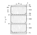
- the wiring board 3 is formed so that, for example, three solar battery subcells 2 are mounted as shown in FIGS. Further, as shown in FIG. 8, the wiring substrate 3 includes an insulating base material 30 and a plurality of wirings 31 a, 31 b, 31 c, 31 d, 31 e and a metal layer formed on one surface of the base material 30. 31f. A metal layer may also be formed on the other surface of the substrate 30.
- the insulating base material 30 for example, a film-like polyester resin can be used.
- the insulating base material 30 is preferably made of a transparent material or a material that transmits a specific wavelength.
- the metal layer constituting the wiring may be conductive, and for example, a metal such as Cu, Al, Ni, Sn, or Ag and a multilayer of these can be used.
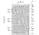
- the wirings 31a to 31f are formed so as to extend in the A direction. As shown in FIGS. 2 and 8, the wirings 31a, 31b, 31c, 31d, 31e and 31f are respectively connected to the n-electrode 23 of the solar battery subcell 2c, the p-electrode 24 of the solar battery subcell 2c, and the solar battery subcell 2d. N electrode 23, p electrode 24 of solar cell subcell 2d, n electrode 23 of solar cell subcell 2e, and p electrode 24 of solar cell subcell 2e. For this reason, three identical wiring patterns (the arrangement pattern of the wirings 31a and 31b, the arrangement pattern of the wirings 31c and 31d, and the arrangement pattern of the wirings 31e and 31f) are formed on the wiring board 3.
- the plurality of wirings 31a are electrically connected by connection portions 31g extending in the B direction. Further, the plurality of wirings 31b and the plurality of wirings 31c are electrically connected by connection portions 31h extending in the B direction. Further, the plurality of wirings 31d and the plurality of wirings 31e are electrically connected by connection portions 31i extending in the B direction. The plurality of wirings 31f are electrically connected by connection portions 31j extending in the B direction. Note that the wirings 31a to 31f and the connection portions 31g to 31j are not formed at positions corresponding to the marks 25a and 25b. The connection portions 31g to 31j are formed of the same layer as the wirings 31a to 31f. Also, alignment marks (not shown) for alignment may be formed on the wiring board 3.
- the solar battery subcells 2c to 2e are mounted on the wiring board 3 via the adhesive layer 6, as shown in FIG. Specifically, as shown in FIGS. 2 and 8, the wirings 31a, 31b, 31c, 31d, 31e, and 31f are respectively connected to the n electrode 23 of the solar cell subcell 2c, the p electrode 24 of the solar cell subcell 2c, and the solar cell.
- the n electrode 23 of the battery subcell 2d, the p electrode 24 of the solar battery subcell 2d, the n electrode 23 of the solar battery subcell 2e, and the p electrode 24 of the solar battery subcell 2e are electrically connected.
- the three solar battery subcells 2 (2c to 2e) are connected in series. Further, as shown in FIG. 2, the three solar cell subcells 2 are arranged such that the dividing plane S1 faces the same direction.
- the sealing material 4 is formed using, for example, a resin transparent to sunlight. Moreover, the sealing material 4 may be formed with polyolefin resin, such as ethylene vinyl acetate, and other resin.
- the transparent substrate 5 is formed using, for example, a PC (polycarbonate resin) or a glass substrate that is transparent to sunlight, but is not particularly limited as long as it is transparent to sunlight.
- the solar cell module 1 can be configured by electrically connecting adjacent solar cell subcells 2 only by mounting the solar cell subcell 2 on the wiring substrate 3, the manufacturing process of the solar cell module 1 is simplified. Can be Thereby, the manufacturing time of the solar cell module 1 can be shortened.
- the n electrode 23 (arrangement pattern of the n electrode 23) is formed point-symmetrically around the center point O1
- the p electrode 24 (arrangement pattern of the p electrode 24) is centered around the center point O1.
- the arrangement pattern of the electrodes of the solar battery subcells 2a and 2b obtained by dividing the solar battery cell 10 by the straight line L1 is the same (or common). That is, solar cell subcells 2a and 2b can be handled as one type of solar cell subcell. Thereby, while being able to simplify the manufacturing process of the solar cell module 1, manufacturing time can be shortened more.
- all the solar battery subcells 2 are mounted on the wiring board 3 so that the dividing plane S1 faces the same direction, so that the appearance of the solar battery module 1 including the array of the solar battery subcells 2 is unified.
- the design of the solar cell module 1 can be improved.
- the n-electrode 23 and the p-electrode 24 are arranged at a predetermined distance from the straight line L1 extending in the B direction through the center point O1.
- the solar battery subcells 2a and 2b are formed in a shape that is not line-symmetric with respect to the axis extending in the B direction, all the solar battery subcells 2 have the dividing plane S1 facing the same direction.
- the wiring board 3 By mounting on the wiring board 3, it is particularly effective because the appearance of the solar cell module 1 can be made uniform.
- the marks 25a and 25b of the portion 10a and the marks 25a and 25b of the portion 10b are arranged at positions that are point-symmetric with respect to the center point O1. Accordingly, when one of the divided solar battery subcells 2a and 2b (parts 10a and 10b) is rotated by 180 degrees, the positions of the marks of the solar battery subcells 2a and 2b coincide. For this reason, since the recognition positions when recognizing the marks 25a and 25b of the solar battery subcells 2a and 2b are the same, the solar battery subcells 2a and 2b can be easily mounted on the wiring board 3.
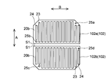
- the solar cell subcell 102 of the second embodiment is obtained by dividing the solar cell 110 shown in FIG. 9 into two as shown in FIG.
- a two-dot chain line (straight line L ⁇ b> 101) in FIG. 9 indicates a division position when dividing the solar battery cell 110.
- a plurality of n electrodes 23, a plurality of p electrodes 24, and a plurality of marks 25a, 25b, 25c and 25d are formed on the back surface 20b side of the solar battery cell 110.
- the marks 25a to 25d are used as alignment marks as in the first embodiment, and can be used to identify the divided solar cell subcells 2a and 2b.
- the n electrode 23 (arrangement pattern of the n electrode 23) is formed point-symmetrically around a predetermined point O101 located at the center of the back surface 20b of the solar battery cell 110.
- the distance between the predetermined point O101 and the center point O1 of the back surface 20b of the solar battery 110 is preferably about 750 ⁇ m (the pitch between the n electrode 23 and the p electrode 24) or less. That is, the center part of the back surface 20b refers to a range from the center point of the back surface 20b to the pitch between the electrodes.
- the p electrode 24 (arrangement pattern of the p electrode 24) is formed point-symmetrically with respect to the point O101.
- the solar cell 110 is divided into two parts 110a and 110b (first part and second part) by a straight line L101 extending in the B direction through the point O101, the n electrode 23 and the p electrode 24 of the part 110a, The n electrode 23 and the p electrode 24 of the portion 110b are formed point-symmetrically with respect to the point O101.
- the marks 25a and 25b (first mark) of the portion 110a and the marks 25c and 25d (second mark) of the portion 110b are arranged at positions that are point-symmetric with respect to the point O101.
- the marks 25a and 25b of the portion 110a and the marks 25c and 25d of the portion 110b are formed in different shapes.
- the marks 25a and 25c are formed in a circular shape and a diamond shape (a shape obtained by rotating a square shape by 45 degrees), respectively.
- the marks 25b and 25d are formed in a quadrangular shape and a triangular shape, respectively.
- solar cell subcells 102a and 102b (first back electrode type solar cell subcell and second back electrode type solar cell subcell) obtained by dividing solar cell 110 are treated as the same solar cell subcell. And can be identified by the marks 25a to 25d. Only one of the pair of marks 25a and 25c or the pair of marks 25b and 25d may have a different shape. For example, even if the mark 25a and the mark 25c have different shapes and the mark 25b and the mark 25d have the same shape, the solar cell subcells 102a and 102b can be identified by the shape identification of the mark 25a and the mark 25c. .
- the predetermined point O101 coincides with the center point O1 of the back surface 20b of the solar battery cell 110, but from the center point O1 due to manufacturing tolerances or the like. It may shift.
- the state where the point O101 is shifted to the right side of FIG. 9 with respect to the center point O1 is exaggerated.
- the point O101 which is the center point of the electrode arrangement pattern is shifted to the right side with respect to the center point O1 of the solar battery 110, for example, the n electrode 23, the p electrode 24 and the marks 25a to 25d are on the right side. It is formed in a shifted state.
- the marks 25a and 25b of the portion 110a (solar cell subcell 102a) and the marks 25c and 25d of the portion 110b (solar cell subcell 102b) are formed in different shapes. Thereby, it can be easily identified from the shape of the mark whether the divided solar battery subcell 102 is the solar battery subcell 102a (part 110a) or the solar battery subcell 2b (part 10b).
- the appearance of the solar cell subcell 102 can be made more uniform, and the design of the solar cell module can be improved. It can be improved further.
- the solar cell subcell 202 (see FIGS. 14 and 15) of the third embodiment is obtained by dividing the solar cell 210 shown in FIG. 13 into two.
- a two-dot chain line (straight line L201) in FIG. 13 indicates a division position when the solar battery cell 210 is divided.
- a plurality of n electrodes 23, a plurality of p electrodes 24, a plurality of marks 225a, 225b, 225c, 225d, 225e, 225f, 225g and 225h are formed on the back surface 20b side of the solar battery cell 210.
- the n electrode 23 is formed point-symmetrically around a predetermined point O101 located at the center of the back surface 20b of the solar battery cell 210.
- the p-electrode 24 is formed point-symmetrically around a predetermined point O101 located at the center.
- the marks 225a to 225d (first mark) of the part 210a (first part) of the solar battery cell 210 and the marks 225e to 225h (second mark) of the part 210b (second part) of the solar battery cell 210 are defined. These are arranged at positions that are point-symmetric with respect to a predetermined point O101 located at the center.
- the center part of the back surface 20b means the range of the pitch (about 750 micrometers) between electrodes from the center point of the back surface 20b.
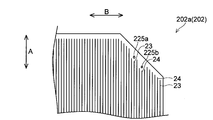
- the mark 225b is arranged in the vicinity of the mark 225a.
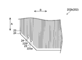
- the mark 225f is disposed in the vicinity of the mark 225e. That is, two marks are provided in one of the corner portions of the solar battery subcell 202.
- the mark 225a and the mark 225e which are arranged at positions that are point-symmetric with respect to a predetermined point O101, are formed in different shapes.
- the mark 225b and the mark 225f arranged at positions that are point-symmetric with each other are formed in different shapes.
- the marks 225a and 225e are formed in an elliptical shape
- the marks 225b and 225c are formed in a perfect circle shape.
- the mark 225 a is disposed on the extension line of the n-electrode 23, and the mark 225 b is disposed on the extension line of the p-electrode 24.
- the mark 225e is disposed on the extension line of the n-electrode 23, and the mark 225f is disposed on the extension line of the p-electrode 24.
- the marks 225c, 225d, 225g, and 225h may all have the same shape or may be formed in different shapes. Further, the marks 225d and 225h may not be formed.
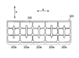
- the wiring board 203 is formed so that the solar battery subcells 202 are mounted in the A direction and the B direction (in a matrix). All the solar battery subcells 202 are connected in series by the wiring board 203. Specifically, in one set (three) of solar cell subcells 202 arranged in the A direction, solar cell subcells 202 adjacent in the A direction are connected in series as in the first and second embodiments. Has been. For example, five sets of solar cell subcells 202 connected in series in the A direction are mounted on the wiring board 203 in the B direction, and adjacent sets are connected in series.
- a current flows from the upper side to the lower side in the region 203a of the wiring board 203, and a current flows from the lower side to the upper side in the region 203b.
- the thick arrow of FIG. 16 has shown the direction through which an electric current flows. In FIG. 16, the wiring of the wiring board is omitted.
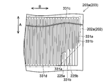
- the wiring board 203 includes a plurality of wirings 331a electrically connected to the n-electrode 23 and a plurality of wirings 331b electrically connected to the p-electrode 24, as shown in FIGS.
- the plurality of wirings 331a are electrically connected by the connection portion 331c
- the plurality of wirings 331b are electrically connected by the connection portion 331d.
- the connecting portion 331c is disposed above the wirings 331a and 331b
- the connecting portion 331d is disposed below the wirings 331a and 331b.
- the connection portion 331c is disposed below the wirings 331a and 331b
- the connection portion 331d is disposed above the wirings 331a and 331b.
- the solar battery subcell 202a when the solar battery subcell 202a is mounted in the region 203a, as shown in FIG. 17, the mark 225b of the solar battery subcell 202a and the wiring 331b of the wiring board 203 overlap, and the mark 225a and the wiring 331a do not overlap.
- the solar cell subcell 202a when the solar cell subcell 202a is mounted in the region 203b, as shown in FIG. 18, the mark 225a and the wiring 331a overlap, and the mark 225b and the wiring 331b do not overlap.
- the solar battery subcell 202b when the solar battery subcell 202b is mounted in the region 203a, the mark 225f and the wiring 331b overlap, and the mark 225e and the wiring 331a do not overlap.
- the solar battery subcell 202b is mounted in the region 203b, the mark 225e and the wiring 331a overlap, and the mark 225f and the wiring 331b do not overlap.
- one of the marks 225a and 225b does not overlap the wirings 331a and 331b.
- one of the marks 225e and 225f does not overlap with the wirings 331a and 331b.
- the mark 225a is disposed on the extension line of the n-electrode 23, and the mark 225b is disposed on the extension line of the p-electrode 24.
- one of the marks 225a and 225b does not overlap the wiring of the wiring board 203.
- the solar cell subcell 202a is mounted on the wiring substrate 203, for example, when the alignment mark is recognized through the solar cell subcell 202a using infrared rays or the like, both the marks 225a and 225b cannot be recognized. There is no. The same applies to solar cell subcell 202b (marks 225e and 225f).
- one set (three) of the solar cell subcells 202 arranged in the A direction is configured by only one of the solar cell subcells 202a and 202b. It is preferable to do. Furthermore, it is more preferable that all the solar cell subcells 202 mounted on one wiring board 203 (or included in one solar cell module) are configured by only one of the solar cell subcells 202a and 202b. If comprised in this way, the uniformity of the external appearance of the solar cell subcell 202 can be given further.
- the present invention is not limited to this, and a p-type silicon substrate may be used, or a semiconductor substrate other than a silicon substrate may be used. Also good.
- the back electrode type solar cell is not limited to the structure of the present embodiment, and includes, for example, a structure such as MWT (metal wrap through) or EWT (emitter wrap through) that draws an electrode to the back surface through a through hole. It is.
- the mark 25a of the solar battery subcell 102a and the mark 25c of the solar battery subcell 102b are formed in different shapes, and the mark 25b of the solar battery subcell 102a and the mark 25d of the solar battery subcell 102b are formed.
- the present invention is not limited to this.
- the marks 25a and 25c are formed at positions that are not point-symmetric with respect to each other (position slightly shifted), the solar battery subcells 102a and 102b can be identified from the positions of the marks. Therefore, the marks 25a and 25c may have the same shape. The same applies to the marks 25b and 25d. That is, even when at least one position of the marks 25a to 25d is shifted and all the shapes are matched, even when at least one shape is different without shifting all the positions, Battery subcells 102a and 102b can be identified.
- n electrodes and the p electrodes of the solar battery subcell are electrically connected on the wiring board, but the present invention is not limited to this. You may provide a connection part in the back surface of a solar cell subcell, and you may electrically connect n electrodes and p electrodes on a solar cell subcell.
- the solar cell subcell is formed in a substantially rectangular shape.
- the present invention is not limited thereto, and the solar cell subcell may be formed in a shape other than a substantially rectangular shape.
- a substantially square photovoltaic cell is 4 It may be divided into two solar cell subcells.
- SYMBOLS 1 Solar cell module 2, 102, 202 Solar cell subcell (back surface electrode type solar cell subcell) 3, 203 Wiring substrate 10, 110, 210 Solar cell (back electrode type solar cell) 10a, 110a, 210a part (first part) 10b, 110b, 210b part (second part) 20a Light-receiving surface 20b Back surface 23 n-electrode 24 p-electrode 25a, 25b Mark (first mark, second mark) 25c, 25d mark (second mark) 102a Solar cell subcell (first back electrode type solar cell subcell) 102b Solar cell subcell (second back electrode type solar cell subcell) 225a to 225d mark (first mark) 225e to 225h mark (second mark) L1, L101, L201 Straight line O1 Center point O101 point (predetermined point) S1 Split surface
Landscapes
- Photovoltaic Devices (AREA)
Abstract
太陽電池サブセルの種類が多くなるのを抑制しながら、太陽電池モジュールの製造時間の短縮および発電効率の向上を実現することが可能な裏面電極型太陽電池セルを提供する。この裏面電極型太陽電池セル(10)では、n電極(23)の配置パターンは裏面(20b)の中心点(O1)を中心として点対称であり、p電極(24)の配置パターンは中心点を中心として点対称であり、n電極およびp電極は、中心点を通りB方向に延びる直線(L1)から所定の距離を隔てて配置されている。
Description
この発明は、裏面電極型太陽電池セル、裏面電極型太陽電池サブセルおよび太陽電池モジュールに関し、特に、受光面とは反対側に配置される裏面に、n電極およびp電極が設けられた裏面電極型太陽電池セル、裏面電極型太陽電池サブセルおよび太陽電池モジュールに関する。
従来、受光面とは反対側に配置された裏面に、n電極およびp電極が設けられた裏面電極型太陽電池が知られている(例えば特許文献1参照)。上記特許文献1には、複数の太陽電池ウェハ(裏面電極型太陽電池セル)と、複数の太陽電池ウェハを電気的に接続する配線基板とを備えた太陽電池モジュールが開示されている。この太陽電池ウェハでは、受光面側に電極を設けず、裏面側にn電極およびp電極を設けている。このため、太陽電池ウェハの受光面積が小さくならないので、太陽電池ウェハの発電効率(=発電量/面積)を向上させることが可能である。
しかしながら、屋根材に一体的に製造された屋根材一体型太陽電池モジュールなどにおいては、太陽電池モジュールのサイズを太陽電池ウェハのサイズから決めることができない場合がある。この場合、太陽電池ウェハを太陽電池モジュールに敷き詰めることができず、太陽電池モジュールの有効面積率(=太陽電池ウェハの面積/太陽電池モジュールの面積)が小さくなる。これにより、上記のように太陽電池ウェハの発電効率を向上させたとしても、太陽電池モジュールの発電効率(=発電量/太陽電池モジュールの面積)は低下してしまう可能性がある。
そこで、有効面積率を大きくすることが可能な太陽電池モジュールが提案されている(例えば特許文献2参照)。上記特許文献2には、台形状の太陽電池素子(太陽電池サブセル)と五角形状の太陽電池素子とを組み合わせて配列することにより有効面積率を大きくした太陽電池モジュールが開示されている。この台形状の太陽電池素子および五角形状の太陽電池素子は六角形状の太陽電池セルをそれぞれ異なる位置で2分割することにより得られる。
また、この太陽電池モジュールでは、太陽電池素子の受光面と裏面とに互いに異なる極性の電極がそれぞれ設けられている。そして、太陽電池素子の受光面側の電極は、隣接する太陽電池素子の裏面側の電極に接続線を用いて電気的に接続されている。
しかしながら、上記特許文献2では、太陽電池素子の受光面に電極が設けられており、また、その電極に接続される接続線も太陽電池素子の受光面に配置されるため、電極および接続線が配置される太陽電池素子の受光面の領域には光が入射せず発電しないため、太陽電池素子の発電効率は向上できない。また、隣接する太陽電池素子(太陽電池サブセル)同士を電気的に接続する際に、受光面側と裏面側との両方に接続線を取り付ける必要がある。このため、太陽電池モジュールの製造に時間がかかるという問題点がある。
また、台形状の太陽電池素子と五角形状の太陽電池素子とが必要であるので、太陽電池素子の種類が多くなるという問題点がある。
この発明は、上記のような課題を解決するためになされたものであり、この発明の目的は、太陽電池サブセルの種類が多くなるのを抑制しながら、太陽電池モジュールの製造時間の短縮および発電効率の向上を実現することが可能な裏面電極型太陽電池セル、裏面電極型太陽電池サブセルおよび太陽電池モジュールを提供することである。
上記目的を達成するために、この発明の裏面電極型太陽電池セルは、光を受光する受光面と、受光面とは反対側に配置された裏面と、裏面側に設けられ、第1の方向に交互に配置されるn電極およびp電極と、を備え、n電極の配置パターンは裏面の中心部に位置する所定の点を中心として点対称であり、p電極の配置パターンは所定の点を中心として点対称であり、n電極およびp電極は、所定の点を通り第1の方向に延びる直線から所定の距離を隔てて配置されている。
なお、本明細書中において、「裏面の中心部」とは裏面の中心点からn電極とp電極との電極間ピッチに相当する距離程度の範囲のことをいう。また、「電極の配置パターンは点対称である」とは、電極の形状(長さ、幅等)が完全に点対称である場合だけでなく、裏面電極型太陽電池セルを分割して得られる裏面電極型太陽電池サブセルを180度回転させたときに同一の配線基板(配線パターン)に実装可能な電極の配置パターンも含む。
この裏面電極型太陽電池セルでは、上記のように、裏面側にn電極およびp電極を設けることによって、受光面積が小さくなるのを抑制することができる。また、隣接する裏面電極型太陽電池サブセル同士を電気的に接続する場合、裏面側だけで配線することができる。
また、上記のように、n電極の配置パターンは所定の点を中心として点対称であり、p電極の配置パターンは所定の点を中心として点対称であることによって、所定の点を通り第1の方向に延びる上記直線で裏面電極型太陽電池セルを分割して得られる裏面電極型太陽電池サブセルの電極の配置パターンが同一(または共通)になる。
また、上記のように、n電極およびp電極を、所定の点を通り第1の方向に延びる直線から所定の距離を隔てて配置する。これにより、所定の点を通り第1の方向に延びる直線で裏面電極型太陽電池セルを分割した際に、分割時の応力によりn電極およびp電極が剥がれたり曲がったりするのを抑制することができる。
上記裏面電極型太陽電池セルにおいて、好ましくは、上記直線により分けられる第1部分および第2部分を含み、第1部分は第1の方向に延びる軸に対して線対称にならない形状に形成され、第2部分は第1の方向に延びる軸に対して線対称にならない形状に形成されている。
上記裏面電極型太陽電池セルにおいて、好ましくは、所定の点は裏面の中心点である。
上記裏面電極型太陽電池セルにおいて、好ましくは、上記直線により分けられる第1部分および第2部分を含み、第1部分には第1マークが設けられ、第2部分には第2マークが設けられ、第1マークおよび第2マークは所定の点を中心として互いに点対称となる位置に配置されている。この場合、分割後の裏面電極型太陽電池サブセル(第1部分および第2部分)を配線基板に実装する際に第1マークおよび第2マークを位置合わせ用のアライメントマークとして用いれば、裏面電極型太陽電池サブセル(第1部分および第2部分)を容易に配線基板に実装することができる。
上記第1部分に第1マークが設けられ、第2部分に第2マークが設けられている裏面電極型太陽電池セルにおいて、好ましくは、第1マークおよび第2マークは互いに異なる形状に形成されている。このように構成すれば、マーク(第1マークおよび第2マーク)の形状から、分割後の裏面電極型太陽電池サブセルが第1部分であるか第2部分であるかを容易に識別することができる。
上記第1部分に第1マークが設けられ、第2部分に第2マークが設けられている裏面電極型太陽電池セルにおいて、好ましくは、第1マークおよび第2マークの各々は複数設けられており、第1マークの少なくとも1つおよび第2マークの少なくとも1つはn電極およびp電極の一方の延長線上に配置され、第1マークの残りの少なくとも1つおよび第2マークの残りの少なくとも1つはn電極およびp電極の他方の延長線上に配置されている。
この発明の裏面電極型太陽電池サブセルは、上記の構成の裏面電極型太陽電池セルを上記直線の位置で分割することにより形成される。
この発明の太陽電池モジュールは、上記の構成の裏面電極型太陽電池サブセルを複数と、複数の裏面電極型太陽電池サブセルが実装される配線基板と、を備え、全ての裏面電極型太陽電池サブセルの分割面が同じ方向を向くように配置されている。
上記太陽電池モジュールにおいて、好ましくは、配線基板には、第1の方向と直交する第2の方向に裏面電極型太陽電池サブセルが奇数個配置されている。
上記太陽電池モジュールにおいて、好ましくは、配線基板には、裏面電極型太陽電池セルを上記直線の位置で分割することにより得られた第1の裏面電極型太陽電池サブセルおよび第2の裏面電極型太陽電池サブセルの一方だけが実装されている。
以上のように、本発明によれば、裏面側にn電極およびp電極を設けることによって、受光面積が小さくなるのを抑制することができるので、裏面電極型太陽電池サブセルの発電効率(=発電量/面積)を向上させることができる。また、隣接する裏面電極型太陽電池サブセル同士を電気的に接続する場合、裏面側だけで配線することができるので、太陽電池モジュールの製造工程を簡略化することができる。これにより、太陽電池モジュールの製造時間を短縮することができる。また、裏面電極型太陽電池サブセルを配線基板に実装することにより太陽電池モジュールを構成すれば、太陽電池モジュールの製造工程をより簡略化することができる。これにより、太陽電池モジュールの製造時間をより短縮することができる。
また、上記のように、n電極の配置パターンは所定の点を中心として点対称であり、p電極の配置パターンは所定の点を中心として点対称であることによって、所定の点を通る直線で裏面電極型太陽電池セルを分割して得られる裏面電極型太陽電池サブセルの電極の配置パターンが同一(または共通)になる。すなわち、裏面電極型太陽電池セルを分割した場合に得られる複数の裏面電極型太陽電池サブセルを1種類の裏面電極型太陽電池サブセルとして扱うことができる。これにより、太陽電池モジュールの製造工程をさらに簡略化することもでき、製造時間をさらに短縮することができる。また、このような裏面電極型太陽電池サブセルを同一方向に配置して太陽電池モジュールを構成すれば、裏面電極型太陽電池サブセルの配列に統一感を持たせることができ、太陽電池モジュールの意匠性を向上させることができる。
また、裏面電極型太陽電池セルを分割して得られる裏面電極型太陽電池サブセルを用いて、太陽電池モジュールを構成する場合、第1の方向に直交する方向(第2の方向)に裏面電極型太陽電池サブセルを例えば奇数個配置することもできる。すなわち、裏面電極型太陽電池セルの半分のサイズ刻みで第2の方向に裏面電極型太陽電池サブセルを敷き詰めることができる。これにより、太陽電池モジュールの有効面積率(=太陽電池サブセルの面積/太陽電池モジュールの面積)を大きくすることができるので、太陽電池モジュールの発電効率(=発電量/太陽電池モジュールの面積)を向上させることができる。
また、上記のように、n電極およびp電極を、所定の点を通り第1の方向に延びる直線から所定の距離を隔てて配置する。これにより、裏面電極型太陽電池セルを所定の点を通り第1の方向に延びる直線で分割する場合に、分割時の応力によりn電極およびp電極が剥がれたり曲がったりするのを抑制することができる。このため、裏面電極型太陽電池サブセルの発電効率が低下したり、その電極が隣接する電極や分割面に接触することにより短絡やリークが発生するのを防止することができる。
以下、本発明の実施形態について図面を参照して説明する。なお、理解を容易にするために、断面図であってもハッチングを施さない場合がある。
(第1実施形態)
図1~図8を参照して、本発明の第1実施形態による太陽電池モジュール1の構造について説明する。
図1~図8を参照して、本発明の第1実施形態による太陽電池モジュール1の構造について説明する。
本発明の第1実施形態による太陽電池モジュール1は図1に示すように、複数(例えば3つ)の裏面電極型太陽電池サブセル(以後、単に太陽電池サブセルと称する)2と、複数の太陽電池サブセル2が実装される配線基板3と、太陽電池サブセル2の表面を覆う封止材4と、封止材4上に配置された透明基板5とを備えている。なお、太陽電池サブセル2は、1つの太陽電池モジュール1において、1つ、2つまたは4つ以上設けられていてもよい。また、太陽電池モジュール1は、配線基板3の裏面側を覆う封止材および裏面フィルム(図示せず)を含んでいてもよい。また、太陽電池モジュール1は、配線基板3および透明基板5の周縁部を固定する枠体(図示せず)などを含んでいてもよく、屋根材に一体的に形成されていてもよい。
太陽電池サブセル2は図2に示すように、例えば長方形状の2つのコーナー部を切り欠いた形状に形成されている。例えば、太陽電池サブセル2の長辺方向(B方向)の長さは約156mmであり、短辺方向(A方向)の長さは約78mmである。また、太陽電池サブセル2、および後述する裏面電極型太陽電池セル10は、図3に示すように、半導体基板20と、半導体基板20の受光面20a上に設けられた反射防止膜21と、半導体基板20の裏面(受光面20aとは反対側の面)20b上に設けられたパッシベーション層22、n電極23およびp電極24とを含んでいる。
半導体基板20は例えばn型の単結晶シリコン基板を用いて形成されている。また、半導体基板20はn型導電領域20cと、半導体基板20の裏面20b側に設けられ、n型導電領域20cよりも高濃度のn型不純物を有するn型拡散領域20dと、半導体基板20の裏面20b側に設けられp型不純物を有するp型拡散領域20eとを含んでいる。
n型拡散領域20dおよびp型拡散領域20eの各々は、太陽電池サブセル2の例えば短手方向(A方向(第2の方向))に延びる帯状に形成されている。また、n型拡散領域20dおよびp型拡散領域20eはA方向と直交するB方向(第1の方向)に交互に配置されている。なお、図3では、n型拡散領域20dおよびp型拡散領域20eを2つずつ示したが、n型拡散領域20dおよびp型拡散領域20eは多数(例えば数十個以上)配置されていてもよい。
n電極23はパッシベーション層22の開口部22aを介して、n型拡散領域20dにオーミック接触されている。同様に、p電極24はパッシベーション層22の開口部22aを介して、p型拡散領域20eにオーミック接触されている。
また、n電極23およびp電極24の各々は図4に示すように、例えばA方向に延びる帯状に形成されている。また、n電極23およびp電極24は、B方向に交互に配置されている。また、n電極23およびp電極24の電極間ピッチは、例えば750μmである。なお、第1実施形態および後述する第2実施形態では、理解を容易にするために、n電極23、p電極24、配線基板3の配線の数を少なくして図示している。
また、太陽電池サブセル2は、図5に示した例えば正方形状の4つのコーナー部を切り欠いた形状の裏面電極型太陽電池セル(以後、単に太陽電池セルと称する)10を、図6に示すように2つに分割(切断)することにより得られる。図5の2点鎖線(直線L1)は、太陽電池セル10を分割する際の分割位置を示している。
なお、太陽電池セル10は、たとえば、図7に示した略円形状の半導体ウェハ11を分割位置C1(図7の2点鎖線)で分割(切断)した後、一般的なウェハ製造プロセスを用いて、n型拡散領域20d、p型拡散領域20e、反射防止膜21、パッシベーション層22、n電極23、p電極24、マーク25aおよび25bが形成されたものである。
ここで、図5に示すように、n電極23(n電極23の配置パターン)は太陽電池セル10の裏面20bの中心点O1を中心として点対称(180度回転対称)に形成されている。同様に、p電極24(p電極24の配置パターン)、マーク25aおよび25bは中心点O1を中心として点対称にそれぞれ形成されている。すなわち、太陽電池セル10を、中心点O1を通りB方向に延びる直線L1で2つの部分10aおよび10b(第1部分および第2部分)に分けると、部分10aのn電極23、p電極24、マーク25aおよび25b(第1マーク)と、部分10bのn電極23、p電極24、マーク25aおよび25b(第2マーク)とは、中心点O1を中心として互いに点対称に形成されている。また、太陽電池セル10(部分10aおよび10b)の外形も、中心点O1を中心として概ね点対称に形成されている。
このため、図6に示すように、太陽電池セル10を分割して得られる太陽電池サブセル2aおよび2bは、一方を180度回転すると、他方と同じ形状(外形、電極の配置パターン)になる。なお、太陽電池サブセル2aおよび2bは太陽電池セル10の部分10aおよび10bにそれぞれ対応している。また、太陽電池サブセル2aおよび2bの各々は、たとえば、B方向に延びる軸(図示せず)に対して線対称にならない形状に形成される。
マーク25aとマーク25bとは互いに異なる形状に形成されていてもよい。例えば、マーク25aは円(真円)形状に形成されており、マーク25bは四角形状に形成されている。なお、マーク25aおよび25bは、太陽電池サブセル2を配線基板3に実装する際に位置合わせ用のアライメントマークとして用いてもよい。この場合は、マーク25aおよび25bは図4に示すように、太陽電池サブセル2のうちの対角に位置する2つのコーナー部にそれぞれ形成されていることが、より精度の高い位置合わせを実現できるため好ましい。
また、図5に示すように、n電極23、p電極24、マーク25aおよび25bは、中心点O1を通りB方向に延びる直線L1(言い換えると、太陽電池サブセル2の分割面S1(図6参照))から所定の距離を隔てて配置されている。すなわち、n電極23、p電極24、マーク25aおよび25bは、直線L1上には形成されていない。
配線基板3は、図2および図8に示すように、例えば3つの太陽電池サブセル2が搭載されるように形成されている。また、配線基板3は、図8に示すように、絶縁性の基材30と、基材30の一方面上に形成された金属層からなる複数の配線31a、31b、31c、31d、31eおよび31fとを含んでいる。なお、基材30の他方面上にも金属層が形成されていてもよい。絶縁性の基材30は、たとえばフィルム状のポリエステル系樹脂を使用することができる。また、太陽電池サブセル2と配線基板3との位置合わせを容易にするために、絶縁性の基材30は透明または特定の波長に対して透過する材質であることが好ましい。配線を構成する金属層は導電性であればよく、たとえばCu、Al、Ni、Sn、Agなどの金属およびこれらを複層としたものを使用することができる。
配線31a~31fはA方向に延びるように形成されている。また、図2および図8に示すように、配線31a、31b、31c、31d、31eおよび31fは、それぞれ、太陽電池サブセル2cのn電極23、太陽電池サブセル2cのp電極24、太陽電池サブセル2dのn電極23、太陽電池サブセル2dのp電極24、太陽電池サブセル2eのn電極23、および、太陽電池サブセル2eのp電極24に対応するように形成されている。このため、配線基板3には同一の配線パターン(配線31aおよび31bの配置パターン、配線31cおよび31dの配置パターン、配線31eおよび31fの配置パターン)が3つ形成されることになる。
また、複数の配線31aはB方向に延びる接続部31gにより電気的に接続されている。また、複数の配線31bおよび複数の配線31cはB方向に延びる接続部31hにより電気的に接続されている。また、複数の配線31dおよび複数の配線31eはB方向に延びる接続部31iにより電気的に接続されている。また、複数の配線31fはB方向に延びる接続部31jにより電気的に接続されている。なお、マーク25aおよび25bに対応する位置には、配線31a~31fおよび接続部31g~31jは形成されていない。また、接続部31g~31jは配線31a~31fと同じ層で形成されている。また、配線基板3にも、位置合わせ用のアライメントマーク(図示せず)が形成されていてもよい。
そして、太陽電池サブセル2c~2eは図1に示すように、接着層6を介して配線基板3に実装されている。具体的には、図2および図8に示すように、配線31a、31b、31c、31d、31eおよび31fは、それぞれ、太陽電池サブセル2cのn電極23、太陽電池サブセル2cのp電極24、太陽電池サブセル2dのn電極23、太陽電池サブセル2dのp電極24、太陽電池サブセル2eのn電極23、および、太陽電池サブセル2eのp電極24に電気的に接続されている。これにより、3つの太陽電池サブセル2(2c~2e)が直列に接続されている。また、3つの太陽電池サブセル2は図2に示すように、分割面S1が同じ方向を向くように配置されている。
封止材4は、例えば太陽光に対して透明な樹脂などを用いて形成されている。また、封止材4は、エチレンビニルアセテートなどのポリオレフィン樹脂や、その他の樹脂により形成されていてもよい。
透明基板5は、例えば太陽光に対して透明なPC(ポリカーボネート樹脂)やガラス基板などを用いて形成されているが、太陽光に対して透明であれば特に限定されない。
本実施形態では、上記のように、裏面20b側にn電極23およびp電極24を設けることによって、受光面積が小さくなるのを抑制することができるので、太陽電池サブセル2の発電効率(=発電量/面積)を向上させることができる。また、太陽電池サブセル2を配線基板3に実装するだけで、隣接する太陽電池サブセル2同士を電気的に接続し太陽電池モジュール1を構成することができるので、太陽電池モジュール1の製造工程を簡略化することができる。これにより、太陽電池モジュール1の製造時間を短縮することができる。
また、上記のように、n電極23(n電極23の配置パターン)を中心点O1を中心として点対称に形成し、p電極24(p電極24の配置パターン)を中心点O1を中心として点対称に形成することによって、太陽電池セル10を直線L1で分割して得られる太陽電池サブセル2aおよび2bの電極の配置パターンが同一(または共通)になる。すなわち、太陽電池サブセル2aおよび2bを1種類の太陽電池サブセルとして扱うことができる。これにより、太陽電池モジュール1の製造工程をより簡略化することもできるとともに、製造時間をより短縮することができる。
また、上記のように、全ての太陽電池サブセル2を分割面S1が同じ方向を向くように配線基板3に実装することによって、太陽電池サブセル2の配列からなる太陽電池モジュール1の外観に統一感を持たせることができ、太陽電池モジュール1の意匠性を向上させることができる。
また、上記のように、A方向に太陽電池サブセル2を例えば3個(奇数個)配置して太陽電池モジュール1を構成している。すなわち、例えば太陽電池モジュール1のサイズを太陽電池サブセル2のサイズから決めることができない場合であっても、太陽電池セル10の半分のサイズ刻みでA方向に太陽電池サブセル2を敷き詰めて太陽電池モジュール1を構成することができる。これにより、太陽電池モジュール1の有効面積率(=太陽電池サブセル2の面積/太陽電池モジュール1の面積)を大きくすることができるので、太陽電池モジュール1の発電効率(=発電量/太陽電池モジュール1の面積)を向上させることができる。
また、上記のように、n電極23およびp電極24を、中心点O1を通りB方向に延びる直線L1から所定の距離を隔てて配置する。これにより、太陽電池セル10を直線L1で分割する際に、分割時の応力によりn電極23およびp電極24が剥がれたり曲がったりするのを抑制することができる。このため、太陽電池サブセル2の発電効率が低下したり、剥がれたり曲がったりした電極が隣接する電極や分割面S1に接触することにより短絡やリークが発生するのを防止することができる。
また、上記のように、太陽電池サブセル2aおよび2bがB方向に延びる軸に対して線対称にならない形状に形成される場合は、全ての太陽電池サブセル2を分割面S1が同じ方向を向くように配線基板3に実装することによって、太陽電池モジュール1の外観に統一感を持たせることができるので、特に有効である。
また、上記のように、部分10aのマーク25aおよび25bと部分10bのマーク25aおよび25bとを、中心点O1を中心として互いに点対称となる位置に配置する。これにより、分割後の太陽電池サブセル2aおよび2b(部分10aおよび10b)の一方を180度回転すると、太陽電池サブセル2aおよび2bのマークの位置が一致する。このため、太陽電池サブセル2aおよび2bのマーク25aおよび25bを認識する際の認識位置が同じになるので、太陽電池サブセル2aおよび2bを容易に配線基板3に実装することができる。
(第2実施形態)
この第2実施形態では、図9~図12を参照して、上記第1実施形態と異なり、太陽電池セル110の部分110aおよび110bに、互いに異なる形状のマークを設ける場合について説明する。
この第2実施形態では、図9~図12を参照して、上記第1実施形態と異なり、太陽電池セル110の部分110aおよび110bに、互いに異なる形状のマークを設ける場合について説明する。
第2実施形態の太陽電池サブセル102は、図9に示した太陽電池セル110を、図10示すように2つに分割することにより得られる。図9の2点鎖線(直線L101)は、太陽電池セル110を分割する際の分割位置を示している。
第2実施形態では図9に示すように、太陽電池セル110の裏面20b側には、複数のn電極23、複数のp電極24、複数のマーク25a、25b、25cおよび25dが形成されている。マーク25a~25dは上記第1実施形態と同様にアライメントマークとして用いられるとともに、分割後の太陽電池サブセル2aおよび2bを識別するために用いることができる。
n電極23(n電極23の配置パターン)は太陽電池セル110の裏面20bの中心部に位置する所定の点O101を中心として点対称に形成されている。なお、所定の点O101と太陽電池セル110の裏面20bの中心点O1との距離は約750μm(n電極23およびp電極24の電極間ピッチ)以下であることが好ましい。すなわち、裏面20bの中心部とは、裏面20bの中心点から電極間ピッチ程度の範囲のことをいう。同様に、p電極24(p電極24の配置パターン)は点O101を中心として点対称に形成されている。すなわち、太陽電池セル110を、点O101を通りB方向に延びる直線L101で2つの部分110aおよび110b(第1部分および第2部分)に分けると、部分110aのn電極23およびp電極24と、部分110bのn電極23およびp電極24とは、点O101を中心として互いに点対称に形成されている。
また、部分110aのマーク25aおよび25b(第1マーク)と、部分110bのマーク25cおよび25d(第2マーク)とは点O101を中心として互いに点対称となる位置に配置されている。また、部分110aのマーク25aおよび25bと、部分110bのマーク25cおよび25dとはそれぞれ異なる形状に形成されている。例えば、マーク25aおよび25cは円形状および菱形状(四角形状を45度回転させた形状)にそれぞれ形成されている。また、マーク25bおよび25dは四角形状および三角形状にそれぞれ形成されている。このため、太陽電池セル110を分割して得られる太陽電池サブセル102aおよび102b(第1の裏面電極型太陽電池サブセルおよび第2の裏面電極型太陽電池サブセル)を、同一の太陽電池サブセルとして扱うことが可能であるとともに、マーク25a~25dにより識別することも可能である。なお、マーク25aおよび25cの一対、もしくはマーク25bおよび25dの一対のいずれか一方の対だけが異なる形状であってもよい。たとえば、マーク25aとマーク25cとが異なる形状で、マーク25bとマーク25dとは同じ形状である場合でも、太陽電池サブセル102aと102bとの識別は、マーク25aとマーク25cの形状識別によって可能となる。
ここで、上述した所定の点O101(電極の配置パターンの中心点)は太陽電池セル110の裏面20bの中心点O1と一致していることが好ましいが、製造上の公差などにより中心点O1からずれてしまう場合がある。本実施形態ではその一例として点O101が中心点O1に対して図9の右側にずれた状態を誇張して図に示している。
図9に示すように、電極の配置パターンの中心点である点O101が太陽電池セル110の中心点O1に対して例えば右側にずれると、n電極23、p電極24およびマーク25a~25dが右側にずれた状態で形成される。
この太陽電池サブセル102aおよび102bを上下に交互に配線基板3に実装すると、図11に示すように太陽電池サブセル102aの左右(B方向)の端部の位置と、太陽電池サブセル102bの左右の端部の位置とが揃わなくなる。このため、図12に示すように、1つの配線基板3には一方の太陽電池サブセル102(図では太陽電池サブセル102a)のみを実装してもよい。このように構成すれば、太陽電池サブセル102の左右の端部の位置を揃えることが可能である。
第2実施形態のその他の構造は、上記第1実施形態と同様である。
本実施形態では、上記のように、部分110a(太陽電池サブセル102a)のマーク25aおよび25bと、部分110b(太陽電池サブセル102b)のマーク25cおよび25dとを互いに異なる形状に形成する。これにより、マークの形状から、分割後の太陽電池サブセル102が太陽電池サブセル102a(部分110a)であるか太陽電池サブセル2b(部分10b)であるかを容易に識別することができる。
また、上記のように、配線基板3に太陽電池サブセル102aおよび102bの一方だけを実装することによって、太陽電池サブセル102の外観に統一感をより持たせることができ、太陽電池モジュールの意匠性をより向上させることができる。
第2実施形態のその他の効果は、上記第1実施形態と同様である。
(第3実施形態)
この第3実施形態では、図13~図18を参照して、上記第1および第2実施形態と異なり、マーク225aおよび225eの近傍にそれぞれマーク225bおよび225fを設ける場合について説明する。
この第3実施形態では、図13~図18を参照して、上記第1および第2実施形態と異なり、マーク225aおよび225eの近傍にそれぞれマーク225bおよび225fを設ける場合について説明する。
第3実施形態の太陽電池サブセル202(図14および図15参照)は、図13に示した太陽電池セル210を2つに分割することにより得られる。図13の2点鎖線(直線L201)は、太陽電池セル210を分割する際の分割位置を示している。
第3実施形態では図13に示すように、太陽電池セル210の裏面20b側には、複数のn電極23、複数のp電極24、複数のマーク225a、225b、225c、225d、225e、225f、225gおよび225hが形成されている。
n電極23は太陽電池セル210の裏面20bの中心部に位置する所定の点O101を中心として点対称に形成されている。同様に、p電極24は中心部に位置する所定の点O101を中心として点対称に形成されている。また、太陽電池セル210の部分210a(第1部分)のマーク225a~225d(第1マーク)と、太陽電池セル210の部分210b(第2部分)のマーク225e~225h(第2マーク)とは、中心部に位置する所定の点O101を中心として互いに点対称となる位置に配置されている。なお、裏面20bの中心部とは、裏面20bの中心点から電極間ピッチ(約750μm)程度の範囲のことをいう。
ここで、マーク225bはマーク225aの近傍に配置されている。同様に、マーク225fはマーク225eの近傍に配置されている。すなわち、太陽電池サブセル202のコーナー部のうちの1つには、2つのマークが設けられている。
また、図14および図15に示すように、所定の点O101を中心として互いに点対称となる位置に配置されているマーク225aとマーク225eとは互いに異なる形状に形成されている。また、同様に互いに点対称となる位置に配置されているマーク225bとマーク225fとは互いに異なる形状に形成されている。例えば、マーク225aおよび225eは楕円形状に形成されており、マーク225bおよび225cは真円形状に形成されている。
また、マーク225aはn電極23の延長線上に配置されており、マーク225bはp電極24の延長線上に配置されている。同様に、マーク225eはn電極23の延長線上に配置されており、マーク225fはp電極24の延長線上に配置されている。
なお、マーク225c、225d、225gおよび225hは、全てが同じ形状であってもよいし、互いに異なる形状に形成されていてもよい。また、マーク225dおよび225hは形成されていなくてもよい。
配線基板203は図16に示すように、太陽電池サブセル202がA方向およびB方向に(マトリクス状に)実装されるように形成されている。そして、配線基板203により、全ての太陽電池サブセル202が直列に接続されている。具体的には、A方向に配列される1組(3つ)の太陽電池サブセル202において、A方向に隣接する太陽電池サブセル202同士は、上記第1および第2実施形態と同様、直列に接続されている。そして、配線基板203には例えばA方向に直列に接続された太陽電池サブセル202がB方向に5組配列されて実装されており、隣接する組同士が直列接続されている。このため、例えば配線基板203の領域203aでは上側から下側に電流が流れ、領域203bでは下側から上側に電流が流れる。なお、図16の太矢印は電流の流れる方向を示している。また、図16では、配線基板の配線を省略している。
配線基板203は図17および図18に示すように、n電極23に電気的に接続される複数の配線331aと、p電極24に電気的に接続される複数の配線331bとを含んでいる。また、複数の配線331aは接続部331cにより電気的に接続されており、複数の配線331bは接続部331dにより電気的に接続されている。なお、領域203aでは図17に示すように、接続部331cは配線331aおよび331bの上側に配置されており、接続部331dは配線331aおよび331bの下側に配置されている。その一方、領域203bでは図18に示すように、接続部331cは配線331aおよび331bの下側に配置されており、接続部331dは配線331aおよび331bの上側に配置されている。
このため、例えば太陽電池サブセル202aを領域203aに実装すると図17に示すように、太陽電池サブセル202aのマーク225bと配線基板203の配線331bとが重なり、マーク225aと配線331aとは重ならない。その一方、太陽電池サブセル202aを領域203bに実装すると図18に示すように、マーク225aと配線331aとが重なり、マーク225bと配線331bとは重ならない。同様に、例えば太陽電池サブセル202bを領域203aに実装すると、マーク225fと配線331bとが重なり、マーク225eと配線331aとは重ならない。また、太陽電池サブセル202bを領域203bに実装すると、マーク225eと配線331aとが重なり、マーク225fと配線331bとは重ならない。
このように、太陽電池サブセル202を配線基板203の領域203aおよび203bのいずれの領域に実装したとしても、マーク225aおよび225bの一方は、配線331aおよび331bに重ならない。同様に、マーク225eおよび225fの一方は、配線331aおよび331bに重ならない。
第3実施形態のその他の構造は、上記第1および第2実施形態と同様である。
本実施形態では、上記のように、マーク225aをn電極23の延長線上に配置し、マーク225bをp電極24の延長線上に配置する。これにより、マーク225aおよび225bの一方は配線基板203の配線に重ならない。これにより、太陽電池サブセル202aを配線基板203に実装する際に、例えば赤外線などを用いて太陽電池サブセル202aを透過してアライメントマークを認識する場合に、マーク225aおよび225bの両方が認識できなくなることはない。なお、太陽電池サブセル202b(マーク225eおよび225f)も同様である。
また、第3実施形態のように太陽電池サブセル202をマトリクス状に配置する場合、A方向に配列される1組(3つ)の太陽電池サブセル202を太陽電池サブセル202aおよび202bの一方だけで構成することが好ましい。さらに、1つの配線基板203に実装される(または1つの太陽電池モジュールに含まれる)全ての太陽電池サブセル202を太陽電池サブセル202aおよび202bの一方だけで構成することがより好ましい。このように構成すれば、太陽電池サブセル202の外観に統一性をさらに持たせることができる。
第3実施形態のその他の効果は、上記第1および第2実施形態と同様である。
なお、今回開示された実施形態は、すべての点で例示であって制限的なものではないと考えられるべきである。本発明の範囲は、上記した実施形態の説明ではなく請求の範囲によって示され、さらに請求の範囲と均等の意味および範囲内でのすべての変更が含まれる。
例えば、上記実施形態では、n型のシリコン基板を用いた例について示したが、本発明はこれに限らず、p型のシリコン基板を用いてもよいし、シリコン基板以外の半導体基板を用いてもよい。また、裏面電極型太陽電池セルも本実施形態の構造に限るものではなく、たとえば、スルーホールによって裏面に電極を引き出すMWT(メタルラップスルー)やEWT(エミッタラップスルー)などの構造のものも含まれる。
また、例えば上記第2実施形態では、太陽電池サブセル102aのマーク25aと太陽電池サブセル102bのマーク25cとを互いに異なる形状に形成するとともに、太陽電池サブセル102aのマーク25bと太陽電池サブセル102bのマーク25dとを互いに異なる形状に形成した例について示したが、本発明はこれに限らない。例えば、マーク25aおよび25cを互いに点対称とならない位置(少しだけずらした位置)に形成すれば、マークの位置から太陽電池サブセル102aおよび102bを識別することができる。このため、マーク25aおよび25cを同じ形状にしてもよい。マーク25bおよび25dも同様である。すなわち、マーク25a~25dのうちの少なくとも1つの位置をずらし、全ての形状を合わせた場合であっても、全ての位置をずらさず、少なくとも1つの形状を異ならせた場合であっても、太陽電池サブセル102aおよび102bを識別することができる。
また、上記実施形態では、太陽電池サブセルのn電極同士、p電極同士が配線基板上で電気的に接続された例について示したが、本発明はこれに限らない。太陽電池サブセルの裏面に接続部を設け、n電極同士、p電極同士を太陽電池サブセル上で電気的に接続してもよい。
また、上記実施形態では、太陽電池サブセルを略長方形状に形成した例について示したが、本発明はこれに限らず、太陽電池サブセルを略長方形状以外の形状に形成してもよい。
また、上記実施形態では、略正方形状の太陽電池セルを2つの裏面電極型太陽電池サブセルに分割する例について示したが、本発明はこれに限らず、略正方形状の太陽電池セルを例えば4つの太陽電池サブセルに分割してもよい。
1 太陽電池モジュール
2、102、202 太陽電池サブセル(裏面電極型太陽電池サブセル)
3、203 配線基板
10、110、210 太陽電池セル(裏面電極型太陽電池セル)
10a、110a、210a 部分(第1部分)
10b、110b、210b 部分(第2部分)
20a 受光面
20b 裏面
23 n電極
24 p電極
25a、25b マーク(第1マーク、第2マーク)
25c、25d マーク(第2マーク)
102a 太陽電池サブセル(第1の裏面電極型太陽電池サブセル)
102b 太陽電池サブセル(第2の裏面電極型太陽電池サブセル)
225a~225d マーク(第1マーク)
225e~225h マーク(第2マーク)
L1、L101、L201 直線
O1 中心点
O101 点(所定の点)
S1 分割面
2、102、202 太陽電池サブセル(裏面電極型太陽電池サブセル)
3、203 配線基板
10、110、210 太陽電池セル(裏面電極型太陽電池セル)
10a、110a、210a 部分(第1部分)
10b、110b、210b 部分(第2部分)
20a 受光面
20b 裏面
23 n電極
24 p電極
25a、25b マーク(第1マーク、第2マーク)
25c、25d マーク(第2マーク)
102a 太陽電池サブセル(第1の裏面電極型太陽電池サブセル)
102b 太陽電池サブセル(第2の裏面電極型太陽電池サブセル)
225a~225d マーク(第1マーク)
225e~225h マーク(第2マーク)
L1、L101、L201 直線
O1 中心点
O101 点(所定の点)
S1 分割面
Claims (10)
- 光を受光する受光面と、
前記受光面とは反対側に配置された裏面と、
前記裏面側に設けられ、第1の方向に交互に配置されるn電極およびp電極と、
を備え、
前記n電極の配置パターンは前記裏面の中心部に位置する所定の点を中心として点対称であり、
前記p電極の配置パターンは前記所定の点を中心として点対称であり、
前記n電極および前記p電極は、前記所定の点を通り前記第1の方向に延びる直線から所定の距離を隔てて配置されていることを特徴とする裏面電極型太陽電池セル。 - 前記直線により分けられる第1部分および第2部分を含み、
前記第1部分は前記第1の方向に延びる軸に対して線対称にならない形状に形成され、
前記第2部分は前記第1の方向に延びる軸に対して線対称にならない形状に形成されていることを特徴とする請求項1に記載の裏面電極型太陽電池セル。 - 前記所定の点は前記裏面の中心点であることを特徴とする請求項1または2に記載の裏面電極型太陽電池セル。
- 前記直線により分けられる第1部分および第2部分を含み、
前記第1部分には第1マークが設けられ、
前記第2部分には第2マークが設けられ、
前記第1マークおよび前記第2マークは前記所定の点を中心として互いに点対称となる位置に配置されていることを特徴とする請求項1~3のいずれか1項に記載の裏面電極型太陽電池セル。 - 前記第1マークおよび前記第2マークは互いに異なる形状に形成されていることを特徴とする請求項4に記載の裏面電極型太陽電池セル。
- 前記第1マークおよび前記第2マークの各々は複数設けられており、
前記第1マークの少なくとも1つおよび前記第2マークの少なくとも1つは前記n電極および前記p電極の一方の延長線上に配置され、
前記第1マークの残りの少なくとも1つおよび前記第2マークの残りの少なくとも1つは前記n電極および前記p電極の他方の延長線上に配置されていることを特徴とする請求項4または5に記載の裏面電極型太陽電池セル。 - 請求項1~6のいずれか1項に記載の裏面電極型太陽電池セルを前記直線の位置で分割することにより形成されることを特徴とする裏面電極型太陽電池サブセル。
- 請求項7に記載の裏面電極型太陽電池サブセルを複数と、
複数の前記裏面電極型太陽電池サブセルが実装される配線基板と、
を備え、
全ての前記裏面電極型太陽電池サブセルの分割面が同じ方向を向くように配置されていることを特徴とする太陽電池モジュール。 - 前記配線基板には、前記第1の方向と直交する第2の方向に前記裏面電極型太陽電池サブセルが奇数個配置されていることを特徴とする請求項8に記載の太陽電池モジュール。
- 前記配線基板には、前記裏面電極型太陽電池セルを前記直線の位置で分割することにより得られた第1の裏面電極型太陽電池サブセルおよび第2の裏面電極型太陽電池サブセルの一方だけが実装されていることを特徴とする請求項8または9に記載の太陽電池モジュール。
Applications Claiming Priority (2)
| Application Number | Priority Date | Filing Date | Title |
|---|---|---|---|
| JP2011045965A JP5214755B2 (ja) | 2011-03-03 | 2011-03-03 | 裏面電極型太陽電池セル、裏面電極型太陽電池サブセルおよび太陽電池モジュール |
| JP2011-045965 | 2011-03-03 |
Publications (1)
| Publication Number | Publication Date |
|---|---|
| WO2012118114A1 true WO2012118114A1 (ja) | 2012-09-07 |
Family
ID=46758044
Family Applications (1)
| Application Number | Title | Priority Date | Filing Date |
|---|---|---|---|
| PCT/JP2012/055060 Ceased WO2012118114A1 (ja) | 2011-03-03 | 2012-02-29 | 裏面電極型太陽電池セル、裏面電極型太陽電池サブセルおよび太陽電池モジュール |
Country Status (3)
| Country | Link |
|---|---|
| JP (1) | JP5214755B2 (ja) |
| TW (1) | TW201242045A (ja) |
| WO (1) | WO2012118114A1 (ja) |
Cited By (2)
| Publication number | Priority date | Publication date | Assignee | Title |
|---|---|---|---|---|
| CN107195696A (zh) * | 2017-05-10 | 2017-09-22 | 晶澳(扬州)太阳能科技有限公司 | 一种mwt太阳能电池片及利用其制成的mwt太阳能电池组件 |
| US20240339551A1 (en) * | 2021-07-22 | 2024-10-10 | Meyer Burger (Germany) Gmbh | Photovoltaic module and method for manufacturing the same |
Families Citing this family (11)
| Publication number | Priority date | Publication date | Assignee | Title |
|---|---|---|---|---|
| GB2508792A (en) | 2012-09-11 | 2014-06-18 | Rec Modules Pte Ltd | Back contact solar cell cell interconnection arrangements |
| JP6313005B2 (ja) * | 2013-09-25 | 2018-04-18 | 京セラ株式会社 | 光電変換素子及び太陽電池モジュール |
| ES2970755T3 (es) | 2014-06-11 | 2024-05-30 | Shinetsu Chemical Co | Célula solar y método para fabricar la célula solar |
| KR102366935B1 (ko) * | 2014-08-07 | 2022-02-23 | 엘지전자 주식회사 | 태양 전지 및 이를 포함하는 태양 전지 모듈 |
| JP6199839B2 (ja) | 2014-09-30 | 2017-09-20 | 信越化学工業株式会社 | 太陽電池及びその製造方法 |
| KR101846442B1 (ko) * | 2016-12-05 | 2018-04-06 | 엘지전자 주식회사 | 태양 전지 및 이를 포함하는 태양 전지 패널 |
| CN120076424A (zh) * | 2017-01-22 | 2025-05-30 | 泰州隆基乐叶光伏科技有限公司 | Ibc电池互联结构 |
| JP6986357B2 (ja) * | 2017-03-24 | 2021-12-22 | 株式会社カネカ | 太陽電池モジュール |
| CN111630666B (zh) | 2018-01-24 | 2023-11-07 | 株式会社钟化 | 用于太阳能电池单元的连接部件组、以及使用该连接部件组的太阳能电池串和太阳能电池模块 |
| CN117117011A (zh) | 2023-09-19 | 2023-11-24 | 晶科能源(海宁)有限公司 | 一种电池片及光伏组件 |
| CN223539600U (zh) * | 2024-09-04 | 2025-11-11 | 珠海富山爱旭太阳能科技有限公司 | 太阳能电池片及印刷网版、光伏组件 |
Citations (3)
| Publication number | Priority date | Publication date | Assignee | Title |
|---|---|---|---|---|
| JP2009088145A (ja) * | 2007-09-28 | 2009-04-23 | Sharp Corp | 太陽電池、太陽電池の製造方法、太陽電池モジュールの製造方法および太陽電池モジュール |
| JP2011066230A (ja) * | 2009-09-17 | 2011-03-31 | Sharp Corp | 太陽電池モジュール基板および太陽電池モジュール |
| JP2011171722A (ja) * | 2010-01-22 | 2011-09-01 | Sharp Corp | 裏面電極型太陽電池セル、配線シート、配線シート付き太陽電池セル、太陽電池モジュールおよび配線シート付き太陽電池セルの製造方法 |
-
2011
- 2011-03-03 JP JP2011045965A patent/JP5214755B2/ja not_active Expired - Fee Related
-
2012
- 2012-02-29 WO PCT/JP2012/055060 patent/WO2012118114A1/ja not_active Ceased
- 2012-03-02 TW TW101107021A patent/TW201242045A/zh unknown
Patent Citations (3)
| Publication number | Priority date | Publication date | Assignee | Title |
|---|---|---|---|---|
| JP2009088145A (ja) * | 2007-09-28 | 2009-04-23 | Sharp Corp | 太陽電池、太陽電池の製造方法、太陽電池モジュールの製造方法および太陽電池モジュール |
| JP2011066230A (ja) * | 2009-09-17 | 2011-03-31 | Sharp Corp | 太陽電池モジュール基板および太陽電池モジュール |
| JP2011171722A (ja) * | 2010-01-22 | 2011-09-01 | Sharp Corp | 裏面電極型太陽電池セル、配線シート、配線シート付き太陽電池セル、太陽電池モジュールおよび配線シート付き太陽電池セルの製造方法 |
Cited By (2)
| Publication number | Priority date | Publication date | Assignee | Title |
|---|---|---|---|---|
| CN107195696A (zh) * | 2017-05-10 | 2017-09-22 | 晶澳(扬州)太阳能科技有限公司 | 一种mwt太阳能电池片及利用其制成的mwt太阳能电池组件 |
| US20240339551A1 (en) * | 2021-07-22 | 2024-10-10 | Meyer Burger (Germany) Gmbh | Photovoltaic module and method for manufacturing the same |
Also Published As
| Publication number | Publication date |
|---|---|
| JP5214755B2 (ja) | 2013-06-19 |
| JP2012182408A (ja) | 2012-09-20 |
| TW201242045A (en) | 2012-10-16 |
Similar Documents
| Publication | Publication Date | Title |
|---|---|---|
| JP5214755B2 (ja) | 裏面電極型太陽電池セル、裏面電極型太陽電池サブセルおよび太陽電池モジュール | |
| KR101823605B1 (ko) | 태양 전지 및 이를 포함하는 태양 전지 패널 | |
| US20110155203A1 (en) | Solar cell module | |
| JP2017510083A (ja) | バイパスダイオードを備える光起電力モジュール | |
| KR101650014B1 (ko) | 태양 전지 및 이를 포함하는 태양 전지 모듈 | |
| JP2013048166A (ja) | 太陽電池モジュール、太陽電池モジュールアレイ、および太陽電池モジュールの製造方法 | |
| KR20180072110A (ko) | 태양 전지 및 이를 포함하는 태양 전지 패널 | |
| WO2012090849A1 (ja) | 太陽電池ストリングおよび太陽電池モジュール | |
| JP2013143529A (ja) | 太陽電池モジュール | |
| KR20200122394A (ko) | 태양 전지 모듈, 유리 건축재 및 태양 전지 모듈의 제조 방법 | |
| US11515436B2 (en) | Photovoltaic device and photovoltaic unit | |
| US20230411546A1 (en) | Solar cell module | |
| JP2015162483A (ja) | 太陽電池セル、太陽電池サブセルおよび太陽電池モジュール | |
| JP2015053303A (ja) | 太陽電池セル、太陽電池モジュール、および太陽電池セルの製造方法。 | |
| KR20190120599A (ko) | 태양전지 모듈 | |
| US12610628B2 (en) | Solar-cell module | |
| US12495622B2 (en) | Solar-cell module | |
| KR20190029421A (ko) | 태양 전지 패널 | |
| WO2017038733A1 (ja) | 光電変換素子 | |
| KR20170124777A (ko) | 태양 전지 모듈 | |
| KR20190043295A (ko) | 분할셀을 이용한 기와 적층 형태의 태양전지 모듈 | |
| WO2025135160A1 (ja) | 太陽電池モジュールおよびその製造方法 | |
| JPH0442974A (ja) | バイパスダイオード付太陽電池 | |
| KR101816183B1 (ko) | 태양 전지 모듈 | |
| CN121587102A (zh) | 发电模块及发电模块的制造方法 |
Legal Events
| Date | Code | Title | Description |
|---|---|---|---|
| 121 | Ep: the epo has been informed by wipo that ep was designated in this application |
Ref document number: 12751769 Country of ref document: EP Kind code of ref document: A1 |
|
| NENP | Non-entry into the national phase |
Ref country code: DE |
|
| 122 | Ep: pct application non-entry in european phase |
Ref document number: 12751769 Country of ref document: EP Kind code of ref document: A1 |