WO2012117972A1 - 薄膜トランジスタおよびその製造方法、並びに表示装置 - Google Patents
薄膜トランジスタおよびその製造方法、並びに表示装置 Download PDFInfo
- Publication number
- WO2012117972A1 WO2012117972A1 PCT/JP2012/054603 JP2012054603W WO2012117972A1 WO 2012117972 A1 WO2012117972 A1 WO 2012117972A1 JP 2012054603 W JP2012054603 W JP 2012054603W WO 2012117972 A1 WO2012117972 A1 WO 2012117972A1
- Authority
- WO
- WIPO (PCT)
- Prior art keywords
- film
- silicon film
- microcrystalline silicon
- tft
- channel layer
- Prior art date
- Legal status (The legal status is an assumption and is not a legal conclusion. Google has not performed a legal analysis and makes no representation as to the accuracy of the status listed.)
- Ceased
Links
Images







Classifications
-
- H—ELECTRICITY
- H10—SEMICONDUCTOR DEVICES; ELECTRIC SOLID-STATE DEVICES NOT OTHERWISE PROVIDED FOR
- H10D—INORGANIC ELECTRIC SEMICONDUCTOR DEVICES
- H10D30/00—Field-effect transistors [FET]
- H10D30/01—Manufacture or treatment
- H10D30/021—Manufacture or treatment of FETs having insulated gates [IGFET]
- H10D30/031—Manufacture or treatment of FETs having insulated gates [IGFET] of thin-film transistors [TFT]
- H10D30/0321—Manufacture or treatment of FETs having insulated gates [IGFET] of thin-film transistors [TFT] comprising silicon, e.g. amorphous silicon or polysilicon
-
- H—ELECTRICITY
- H10—SEMICONDUCTOR DEVICES; ELECTRIC SOLID-STATE DEVICES NOT OTHERWISE PROVIDED FOR
- H10D—INORGANIC ELECTRIC SEMICONDUCTOR DEVICES
- H10D30/00—Field-effect transistors [FET]
- H10D30/01—Manufacture or treatment
- H10D30/021—Manufacture or treatment of FETs having insulated gates [IGFET]
- H10D30/031—Manufacture or treatment of FETs having insulated gates [IGFET] of thin-film transistors [TFT]
- H10D30/0312—Manufacture or treatment of FETs having insulated gates [IGFET] of thin-film transistors [TFT] characterised by the gate electrodes
- H10D30/0316—Manufacture or treatment of FETs having insulated gates [IGFET] of thin-film transistors [TFT] characterised by the gate electrodes of lateral bottom-gate TFTs comprising only a single gate
-
- H—ELECTRICITY
- H10—SEMICONDUCTOR DEVICES; ELECTRIC SOLID-STATE DEVICES NOT OTHERWISE PROVIDED FOR
- H10D—INORGANIC ELECTRIC SEMICONDUCTOR DEVICES
- H10D30/00—Field-effect transistors [FET]
- H10D30/60—Insulated-gate field-effect transistors [IGFET]
- H10D30/67—Thin-film transistors [TFT]
- H10D30/6729—Thin-film transistors [TFT] characterised by the electrodes
- H10D30/673—Thin-film transistors [TFT] characterised by the electrodes characterised by the shapes, relative sizes or dispositions of the gate electrodes
- H10D30/6732—Bottom-gate only TFTs
-
- H—ELECTRICITY
- H10—SEMICONDUCTOR DEVICES; ELECTRIC SOLID-STATE DEVICES NOT OTHERWISE PROVIDED FOR
- H10D—INORGANIC ELECTRIC SEMICONDUCTOR DEVICES
- H10D30/00—Field-effect transistors [FET]
- H10D30/60—Insulated-gate field-effect transistors [IGFET]
- H10D30/67—Thin-film transistors [TFT]
- H10D30/674—Thin-film transistors [TFT] characterised by the active materials
- H10D30/6741—Group IV materials, e.g. germanium or silicon carbide
- H10D30/6743—Silicon
- H10D30/6745—Polycrystalline or microcrystalline silicon
-
- H—ELECTRICITY
- H10—SEMICONDUCTOR DEVICES; ELECTRIC SOLID-STATE DEVICES NOT OTHERWISE PROVIDED FOR
- H10D—INORGANIC ELECTRIC SEMICONDUCTOR DEVICES
- H10D30/00—Field-effect transistors [FET]
- H10D30/60—Insulated-gate field-effect transistors [IGFET]
- H10D30/67—Thin-film transistors [TFT]
- H10D30/6757—Thin-film transistors [TFT] characterised by the structure of the channel, e.g. transverse or longitudinal shape or doping profile
-
- H—ELECTRICITY
- H10—SEMICONDUCTOR DEVICES; ELECTRIC SOLID-STATE DEVICES NOT OTHERWISE PROVIDED FOR
- H10D—INORGANIC ELECTRIC SEMICONDUCTOR DEVICES
- H10D62/00—Semiconductor bodies, or regions thereof, of devices having potential barriers
- H10D62/40—Crystalline structures
-
- H—ELECTRICITY
- H10—SEMICONDUCTOR DEVICES; ELECTRIC SOLID-STATE DEVICES NOT OTHERWISE PROVIDED FOR
- H10P—GENERIC PROCESSES OR APPARATUS FOR THE MANUFACTURE OR TREATMENT OF DEVICES COVERED BY CLASS H10
- H10P14/00—Formation of materials, e.g. in the shape of layers or pillars
- H10P14/20—Formation of materials, e.g. in the shape of layers or pillars of semiconductor materials
- H10P14/24—Formation of materials, e.g. in the shape of layers or pillars of semiconductor materials using chemical vapour deposition [CVD]
-
- H—ELECTRICITY
- H10—SEMICONDUCTOR DEVICES; ELECTRIC SOLID-STATE DEVICES NOT OTHERWISE PROVIDED FOR
- H10P—GENERIC PROCESSES OR APPARATUS FOR THE MANUFACTURE OR TREATMENT OF DEVICES COVERED BY CLASS H10
- H10P14/00—Formation of materials, e.g. in the shape of layers or pillars
- H10P14/20—Formation of materials, e.g. in the shape of layers or pillars of semiconductor materials
- H10P14/34—Deposited materials, e.g. layers
- H10P14/3402—Deposited materials, e.g. layers characterised by the chemical composition
- H10P14/3404—Deposited materials, e.g. layers characterised by the chemical composition being Group IVA materials
- H10P14/3411—Silicon, silicon germanium or germanium
-
- H—ELECTRICITY
- H10—SEMICONDUCTOR DEVICES; ELECTRIC SOLID-STATE DEVICES NOT OTHERWISE PROVIDED FOR
- H10P—GENERIC PROCESSES OR APPARATUS FOR THE MANUFACTURE OR TREATMENT OF DEVICES COVERED BY CLASS H10
- H10P14/00—Formation of materials, e.g. in the shape of layers or pillars
- H10P14/20—Formation of materials, e.g. in the shape of layers or pillars of semiconductor materials
- H10P14/34—Deposited materials, e.g. layers
- H10P14/3451—Structure
- H10P14/3452—Microstructure
- H10P14/3456—Polycrystalline
Definitions
- the present invention relates to a thin film transistor, a manufacturing method thereof, and a display device, and more particularly, to a thin film transistor using a microcrystalline semiconductor film, a manufacturing method thereof, and a display device.
- a thin film transistor (hereinafter abbreviated as “TFT”) is used as a switching element in a pixel formation portion or a semiconductor element constituting a driving circuit.
- TFT thin film transistor
- an amorphous silicon film or a polycrystalline silicon film has been used for the channel layer of such a TFT.
- a microcrystalline silicon film that has a higher mobility than an amorphous silicon film and does not require an annealing treatment such as a polycrystalline silicon film has been used.
- Patent Document 1 as a channel layer of an inverted staggered TFT, first, a first microcrystalline silicon film whose deposition rate is slowed down by increasing the dilution rate of silane gas (SiH 4 ) is formed on a gate insulating film. Form. Next, a second microcrystalline silicon film is formed on the first microcrystalline silicon film by increasing the deposition rate by decreasing the dilution rate of the silane gas.
- the mobility of the TFT is improved by making the crystallinity of the first microcrystalline silicon film close to the gate electrode higher than the crystallinity of the second microcrystalline silicon film.
- hydrofluoric acid aqueous solution having a hydrofluoric acid (HF) concentration of 5% is used.
- a microcrystalline silicon film is a columnar crystal in which crystal grains grow in a direction perpendicular to the substrate, and the physical coupling in the horizontal direction is weak. Therefore, if the second microcrystalline silicon film is immersed in a hydrofluoric acid aqueous solution in order to remove the natural oxide film formed on the surface of the second microcrystalline silicon film, the hydrofluoric acid aqueous solution becomes the second microcrystalline water.
- the gate insulating film is etched by intruding into the first microcrystalline silicon film along the crystal grain boundary from the surface of the silicon film. When the etching of the gate insulating film proceeds, the first and second microcrystalline silicon films are lifted off, and film peeling occurs. If film peeling occurs, a channel layer is not formed and a TFT cannot be manufactured.
- Patent Document 1 describes that the Raman peak intensity ratio of the second microcrystalline silicon film is changed to 3.52 or 6.19 by changing the dilution ratio of the silane gas. For this reason, in Patent Document 1, the natural oxide film is removed with a hydrofluoric acid aqueous solution only for the purpose of making the crystallinity of the second microcrystalline silicon film lower than the crystallinity of the first microcrystalline silicon film. The film peeling that occurs is not considered. For this reason, Patent Document 1 does not disclose a solution for preventing film peeling by increasing resistance to a hydrofluoric acid aqueous solution.
- an object of the present invention is to provide a thin film transistor having a channel layer with high chemical resistance and a manufacturing method thereof with increased mobility.
- Another object of the present invention is to provide a display device that can achieve high definition and high frame rate by using such a thin film transistor.
- a first aspect of the present invention is a thin film transistor formed on an insulating substrate, A gate electrode formed on the insulating substrate; A gate insulating film formed to cover the gate electrode; A channel layer formed on the gate insulating film, The channel layer is A first microcrystalline semiconductor film formed on a surface of the gate insulating film and having a Raman peak intensity ratio of 7.0 or more; And a second microcrystalline semiconductor film formed on the surface of the first microcrystalline semiconductor film and having a Raman peak intensity ratio of 4.5 or less.
- a third microcrystalline semiconductor film serving as a base film for the first microcrystalline semiconductor film is formed on the surface of the gate insulating film.
- An etching stopper layer formed on the surface of the channel layer is further provided.
- a fourth aspect of the present invention is a method of manufacturing a thin film transistor formed on an insulating substrate, Forming a gate electrode on the insulating substrate; Forming a gate insulating film so as to cover the gate electrode; Forming a channel layer on the gate insulating film in a high-density plasma CVD apparatus,
- the step of forming the channel layer includes: Forming a first microcrystalline semiconductor film by setting the pressure in the high-density plasma CVD apparatus to a first pressure value; Forming a second microcrystalline semiconductor film by setting the pressure in the high-density plasma CVD apparatus to a second pressure value lower than the first pressure value.
- the step of forming the channel layer further includes a process of covering an inner wall of the high-density plasma CVD apparatus with a semiconductor film before carrying the insulating substrate into the high-density plasma CVD apparatus.
- the step of forming the channel layer is after the step of covering the inner wall of the high-density plasma CVD apparatus with a semiconductor film, and before the step of forming the first microcrystalline semiconductor film, with argon gas and hydrogen
- the method further includes the step of cleaning the surface of the gate insulating film with gas plasma and forming a third microcrystalline semiconductor film to be a base film of the first microcrystalline silicon film on the surface of the gate insulating film. It is characterized by.
- a seventh aspect of the present invention is the sixth aspect of the present invention,
- the thickness of the third microcrystalline semiconductor film is 3 to 7 nm.
- the first pressure value is 20 mTorr or more, and the second pressure value is 5 mTorr or less.
- a ninth aspect of the present invention is an active matrix display device that displays an image, A plurality of pixel forming portions arranged in a matrix corresponding to a plurality of gate wirings, a plurality of source wirings intersecting with the plurality of gate wirings, and intersections of the plurality of gate wirings and the plurality of source wirings, respectively.
- a display unit comprising: A drive circuit for driving the plurality of pixel formation portions, The pixel formation unit includes a switching element that is turned on or off according to a signal applied to a corresponding gate wiring, The switching element includes the thin film transistor according to the first aspect.
- the drive circuit includes a thin film transistor according to a ninth aspect of the present invention.
- the channel layer of the thin film transistor includes the first microcrystalline semiconductor film formed on the gate insulating film and the second microcrystalline semiconductor formed on the first microcrystalline semiconductor film. Including a membrane. Since the first microcrystalline semiconductor film has a Raman peak intensity ratio of 7.0 or more, crystal grains are grown in a columnar shape. Accordingly, the mobility of the thin film transistor can be set to 0.7 cm 2 / Vsec or more. In addition, since the second microcrystalline semiconductor film has a Raman peak intensity ratio of 4.5 or less, the second microcrystalline semiconductor film contains a large amount of an amorphous component and covers the first microcrystalline semiconductor film. Therefore, even if the channel layer is immersed in a chemical solution, the chemical solution is unlikely to enter the first microcrystalline semiconductor film. Thereby, the chemical
- the third microcrystalline semiconductor film on the surface of the gate insulating film, it is difficult for the incubation layer to grow on the gate insulating film. Accordingly, the crystallinity of the first microcrystalline silicon film formed using the third microcrystalline silicon film as a base film is increased, and the mobility of the thin film transistor can be kept high.
- the natural oxide film formed on the surface of the channel layer is removed without causing film peeling even when the channel layer having the etching stopper layer formed on the surface is immersed in the chemical solution. be able to. Thereby, the adhesion between the channel layer and the etching stopper layer can be improved.
- the second microcrystalline semiconductor film is The film is formed at a second pressure value lower than the first pressure value.
- the first microcrystalline semiconductor film crystal grains grow in a columnar shape, so that the mobility of the thin film transistor is increased.
- the second microcrystalline semiconductor film contains a large amount of an amorphous component, the chemical liquid is covered with the second microcrystalline semiconductor film even if the channel layer is immersed in the chemical liquid. It becomes difficult to penetrate into the crystalline semiconductor film. As a result, a thin film transistor with improved chemical resistance can be manufactured while maintaining high mobility.
- the crystallinity of the first and second microcrystalline silicon films is controlled by changing the pressure in the high-density plasma CVD apparatus, the crystallinity can be accurately controlled.
- the inner wall of the high density plasma CVD apparatus is covered with a semiconductor film.
- the first or second microcrystalline silicon film is formed, residual foreign matter adhering to the inner wall of the high-density plasma CVD apparatus is mixed into the first or second microcrystalline semiconductor film, and the thin film transistor Decreasing the mobility can be suppressed.
- moisture, organic matter, metal particles, etc. adsorbed on the gate insulating film are removed, and the surface of the gate insulating film is cleaned.
- the crystallinity of the first microcrystalline silicon film formed using the third microcrystalline silicon film formed over the gate insulating film as a base film is increased, so that the mobility of the thin film transistor can be kept higher.
- the incubation film grows and the crystallinity of the first microcrystalline silicon film formed thereon is grown. Becomes lower. Further, if the film thickness is thicker than 7 nm, the time for forming the third microcrystalline silicon film becomes longer. Therefore, if the thickness of the third microcrystalline semiconductor film is 3 to 7 nm, these problems are eliminated.
- the mobility of the thin film transistor is set to 0.7 cm 2 / Vsec or more by setting the first pressure value when forming the first microcrystalline semiconductor film to 20 mTorr or more. Can do.
- the second pressure value in forming the second microcrystalline semiconductor film is set to 5 mTorr or less, a hydrofluoric acid aqueous solution is formed in the first semiconductor film covered with the second microcrystalline semiconductor film. Since it becomes difficult to penetrate, the chemical resistance can be increased to 180 seconds or more.
- the thin film transistor according to the first aspect when used as the switching element of the pixel formation portion, the on-current flowing through the thin film transistor is increased.
- the thin film transistor can charge the pixel capacitor with the signal voltage of the image signal in a short time, the number of pixel formation portions can be increased and high definition can be achieved.
- the chemical resistance of the thin film transistor is improved, the display portion including the pixel formation portion can be easily formed.
- the on-current flowing through the thin film transistor according to the first aspect is large.
- the driving circuit is configured using the thin film transistor according to the first aspect, the operating speed of the driving circuit is increased, and a high frame rate is easily achieved.
- the circuit scale of the driver circuit can be reduced, the frame of the display portion can be reduced and the power consumption of the display device can be reduced.
- the chemical resistance of the thin film transistor is improved, a highly reliable driving circuit can be formed.
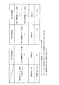
- FIG. 5 is a diagram showing Raman peak intensity ratios of a microcrystalline silicon film, chemical resistance, and TFT mobility for the first to third comparative examples.
- FIG. (A) is sectional drawing which shows the structure of TFT which concerns on a 1st comparative example, (b) shows only the manufacturing process which forms the microcrystal silicon film used as the channel layer of TFT shown to (a).
- FIG. (A) is sectional drawing which shows the structure of TFT which concerns on a 2nd comparative example, (b) shows only the manufacturing process which forms the microcrystal silicon film used as the channel layer of TFT shown to (a).
- FIG. (A) is sectional drawing which shows the structure of TFT which concerns on a 3rd comparative example, (b) shows only the manufacturing process which forms the microcrystal silicon film used as the channel layer of TFT shown to (a).
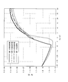
- FIG. 6 is a diagram showing gate voltage-drain current characteristics of TFTs according to the first to third embodiments.
- FIG. 6 is a diagram showing a Raman peak intensity ratio, chemical resistance, and TFT mobility of a microcrystalline silicon film for the first to third embodiments.
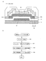
- A) is sectional drawing which shows the structure of TFT concerning the 1st Embodiment of this invention
- (b) is a manufacturing which forms the microcrystal silicon film used as the channel layer of TFT shown to (a) It is a flowchart which shows only a process. It is sectional drawing which shows the structure of TFT which concerns on the modification of 1st Embodiment.
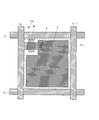
- FIG. 18 is a plan view showing a pattern arrangement in a pixel formation portion provided in the liquid crystal panel of the liquid crystal display device shown in FIG. 17.
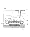
- FIG. 18 is a cross-sectional view of a TFT that functions as a switching element of a pixel formation portion of the liquid crystal display device shown in FIG.
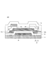
- FIG. 1 is a cross-sectional view showing the configuration of the inverted staggered TFT 10.
- the configuration of the TFT 10 will be described with reference to FIG.
- a gate electrode 20 made of a titanium (Ti) film having a thickness of 100 nm is formed on a glass substrate 15 which is an insulating substrate.
- a gate insulating film 25 made of a silicon nitride film (SiNx) is formed so as to cover the entire glass substrate 15 including the gate electrode 20.
- the film thickness of the gate insulating film 25 is, for example, 410 nm.
- An island-shaped channel layer 30 is formed on the surface of the gate insulating film 25 so as to extend left and right across the gate electrode 20 in plan view.
- the film thickness of the channel layer 30 is, for example, 70 nm.
- the channel layer 30 is made of a microcrystalline silicon film that does not contain impurities. The specific configuration of the channel layer 30 differs for each comparative example and embodiment described later.
- An etching stopper layer 40 made of a silicon nitride film is formed on the surface of the channel layer 30 facing the gate electrode 20.
- the film thickness of the etching stopper layer 40 is, for example, 150 nm.
- An ohmic contact layer 50a extending from the left upper surface of the etching stopper layer 40 to the left end of the channel layer 30, and an ohmic contact extending to cover the right upper surface of the etching stopper layer 40 to the right end of the channel layer 30 A layer 50b is formed.
- These ohmic contact layers 50 a and 50 b are made of a microcrystalline silicon film (n + silicon film) doped with an n-type impurity such as phosphorus (P) at a high concentration, and are separated from each other on the upper surface of the etching stopper layer 40. Yes.
- a drain electrode 60b extending to the top of the film 25 is formed.
- the source electrode 60a is in ohmic contact with the channel layer 30 through the ohmic contact layer 50a
- the drain electrode 60b is in ohmic contact with the channel layer 30 through the ohmic contact layer 50b.
- a passivation film 70 made of a silicon nitride film is formed so as to cover the entire glass substrate 15 including the source electrode 60a and the drain electrode 60b.
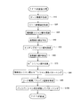
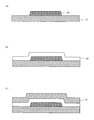
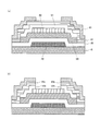
- FIG. 2 is a flowchart showing a process flow for manufacturing the TFT 10 shown in FIG. 3A to FIG. 3C, FIG. 4A to FIG. 4C, FIG. 5A, and FIG. 5B show each manufacturing process of the TFT 10 shown in FIG. It is sectional drawing. 2 and the cross-sectional views shown in FIGS. 3 (a) to 3 (c), 4 (a) to 4 (c), 5 (a) and 5 (b). The manufacturing process of the TFT 10 will be described with reference to FIG.
- a titanium film or a metal film containing titanium as a main component is formed on the glass substrate 15 by a sputtering method.
- the thickness of the titanium film is, for example, 100 nm.
- a metal film such as tungsten (W), molybdenum (Mo), or aluminum (Al), a metal film containing them as a main component, or a metal film formed by stacking them may be formed. .
- a resist pattern is formed on the surface of the titanium film using a photolithography method.
- the gate electrode 20 is formed by etching the titanium film by a wet etching method using a resist pattern (not shown) as a mask. Thereafter, the resist pattern is peeled off. Note that the gate electrode 20 may be formed by etching using a dry etching method instead of the wet etching method.
- a parallel plate chemical vapor deposition (hereinafter referred to as “parallel plate CVD”) apparatus is provided so as to cover the entire glass substrate 15 including the gate electrode 20.
- a silicon nitride film to be the gate insulating film 25 is formed from a source gas containing silane gas and nitrogen gas (N 2 ).
- the film thickness of the silicon nitride film is, for example, 410 nm.
- a silicon oxide (SiO 2 ) film, a silicon oxynitride (SiON) film, or a stacked film thereof may be formed instead of the silicon nitride film.
- a microcrystalline silicon film 31 composed of a plurality of layers is formed on the surface of the gate insulating film 25.
- the microcrystalline silicon film 31 is formed using a high-density plasma CVD apparatus such as a surface wave plasma method or an ICP (Inductively-Coupled-Plasma) method.
- the film thickness of the microcrystalline silicon film 31 is, for example, 70 nm. Note that the structure and film formation conditions of the plurality of layers included in the microcrystalline silicon film 31 are different for each comparative example and embodiment, and will be described later.
- step S40 the natural oxide film formed on the surface of the microcrystalline silicon film 31 is removed.
- the microcrystalline silicon film 31 is immersed in a thin acid solution for 40 seconds, then washed with water and dried. Thereby, the natural oxide film formed on the surface of the microcrystalline silicon film 31 is removed.
- a thin acid aqueous solution in which the microcrystalline silicon film 31 is immersed for example, a hydrofluoric acid aqueous solution having a hydrofluoric acid concentration of 0.5%, buffered hydrofluoric acid, or the like is used.
- the natural oxide film is removed before forming the silicon nitride film to be the etching stopper layer 40 for the following reason.
- step S50 the glass substrate 15 immediately after removal of the natural oxide film is carried into a parallel plate CVD apparatus, and a source gas containing silane gas and ammonia gas (NH 3 ) is used.
- a silicon nitride film 41 is formed on the surface of the microcrystalline silicon film 31.
- the film thickness of the silicon nitride film 41 is 150 nm, for example.
- a resist pattern 45 is formed on the surface of the silicon nitride film 41 at a position facing the gate electrode 20 by photolithography. Using the resist pattern 45 as a mask, the silicon nitride film 41 is etched by dry etching to form an etching stopper layer 40. Note that the etching stopper layer 40 may be formed by etching a silicon oxide film or a silicon oxynitride film.
- step S60 the natural oxide film formed on the surface of the microcrystalline silicon film 31 not covered with the etching stopper layer 40 is removed. Since the method for removing the natural oxide film is the same as that for removing the natural oxide film in step S40, the description thereof is omitted. Note that the time for immersing the microcrystalline silicon film 31 in the hydrofluoric acid aqueous solution is 20 seconds. As described above, the natural oxide film is removed without removing the natural oxide film formed on the surface of the microcrystalline silicon film 31, and an amorphous silicon film 51 described later is formed on the surface of the microcrystalline silicon film 31. This is because when the film is formed, the adhesion between the microcrystalline silicon film 31 and the amorphous silicon film 51 is deteriorated, and the ohmic contact layers 50a and 50b are easily peeled off.
- the amorphous silicon film 51 to be the ohmic contact layers 50a and 50b is formed so as to cover the entire glass substrate 15 including the etching stopper layer 40 and the microcrystalline silicon film 31. Is deposited.
- the amorphous silicon film 51 is an amorphous silicon film (hereinafter referred to as “amorphous silicon film”) doped with an n-type impurity such as phosphorus (P) at a high concentration so that the source electrode 60a and the drain electrode 60b are in ohmic contact with the channel layer 30. , Referred to as “n + silicon film 51”).
- step S80 as shown in FIG. 4C, a resist pattern 55 is formed on the surface of the n + silicon film 51 by using a photolithography technique. Using the resist pattern 55 as a mask, the n + silicon film 51 and the microcrystalline silicon film 31 are continuously etched by dry etching. Thereafter, the resist pattern 55 is peeled off. Thereby, the island-shaped channel layer 30 is formed, and the n + silicon film 51 has the same shape as the channel layer 30.
- a source metal film 61 is formed using a sputtering apparatus.
- the source metal film 61 is, for example, a titanium film or a metal film containing titanium as a main component.
- a resist pattern 65 having an opening above the etching stopper layer 40 is formed on the source metal film 61 by photolithography.
- the source metal film 61 is etched by a wet etching method to form a source electrode 60a and a drain electrode 60b.
- the source metal film 61 may be etched by a dry etching method instead of the wet etching method.
- the n + silicon film 51 is etched by a dry etching method to form two ohmic contact layers 50 a and 50 b separated from each other on the upper surface of the etching stopper layer 40. Since the etching stopper layer 40 made of silicon nitride is formed on the upper surface of the channel layer 30, the etching of the n + silicon film 51 is stopped by the etching stopper layer 40 and the surface of the channel layer 30 is etched. There is no.
- the source electrode 60a extends from the right upper surface of the ohmic contact layer 50a to the left gate insulating film 25 so as to cover the ohmic contact layer 50a
- the drain electrode 60b extends from the left upper surface of the ohmic contact layer 50b to the ohmic contact layer 50b. Covering and extending to the right gate insulating film 25.
- a passivation film 70 made of silicon nitride is formed so as to cover the entire glass substrate 15 including the source electrode 60a and the drain electrode 60b.
- the passivation film 70 is formed by a parallel plate plasma CVD apparatus using a source gas containing silane gas and ammonia gas, and has a film thickness of, for example, 265 nm.
- the glass substrate 15 on which the TFT 10 is formed is heated at 200 ° C. for 1 hour in a nitrogen atmosphere so that the source electrode 60a and the ohmic contact layer 50a and the drain electrode 60b and the ohmic contact layer 50b are in ohmic contact, respectively.
- the TFT 10 shown in FIG. 1 is manufactured through the series of manufacturing steps described above.
- the method for forming the microcrystalline silicon film 31 shown in step S30 of FIG. 2 includes the following four processing steps. That is, a pre-coating process in which the inner wall of the chamber of the high-density plasma CVD apparatus is coated with a silicon film and an argon / hydrogen plasma process are performed to clean the surface of the gate insulating film 25 and form a thin microcrystalline silicon film. Includes a hydrogen plasma treatment, a step of forming a first microcrystalline silicon film having high crystallinity, and a step of forming a second microcrystalline silicon film having lower crystallinity than the first microcrystalline silicon film. Yes. Therefore, these processing steps will be described.
- Gap in the following process conditions refers to the distance between the surface of the glass substrate 15 and the surface of the electrode of the high-density plasma CVD apparatus.
- Microwave frequency 915 MHz
- Power 0.8 W / cm 2
- Pressure 20mTorr
- Gap 90mm SiH 4 flow rate: 400 sccm
- Ar flow rate 600sccm
- Chamber temperature 100 ° C Processing time: 600 sec
- the film thickness is 3 to 7 nm, preferably 4 to 6 nm. Since the thin microcrystalline silicon film is formed by chemical transport described later, the film thickness falls within the range of 3 to 7 nm. If the thickness of the thin microcrystalline silicon film is thinner than 3 nm, the incubation film grows and the crystallinity of the microcrystalline silicon film 31 formed thereon is lowered. In addition, when the film thickness is greater than 7 nm, the formation time of the thin microcrystalline silicon film becomes longer. For this reason, the thickness of the thin microcrystalline silicon film formed by chemical transport is preferably 3 to 7 nm, and more preferably 4 to 6 nm.
- Microwave frequency 915 MHz
- Power 3.2 W / cm 2
- Pressure 20mTorr H 2 flow rate: 48sccm
- Ar flow rate 504 sccm
- Gap 150mm
- Chamber temperature 100 ° C
- Substrate set temperature 200 ° C Processing time: 15msec
- the silicon film adhering to the inner wall of the chamber at the time of pre-coating is chemically transported to form a thin microcrystalline silicon film. Is deposited.
- the crystallinity of the microcrystalline silicon film is evaluated by a Raman peak intensity ratio (Ic / Ia) obtained from a Raman scattering spectrum.
- the microcrystalline silicon film has a peak in which a sharp peak near 520 cm ⁇ 1 due to the crystalline silicon component and a wide peak near 480 cm ⁇ 1 due to the amorphous silicon component are superimposed.
- Ic represents the peak intensity near 520 cm ⁇ 1 in the Raman scattering spectrum
- Ia represents the peak intensity near 480 cm ⁇ 1 .
- the value of Raman peak intensity ratio Ic / Ia represents crystallinity (crystallization rate), and the larger the value of Raman peak intensity ratio Ic / Ia, the more crystallinity (crystallization rate) of the microcrystalline silicon film becomes. It turns out that it is a high film
- the step of forming the microcrystalline silicon film 31 shown in step S30 includes a step of forming a first microcrystalline silicon film having a high crystallization rate, and a step of forming a crystallization rate lower than that of the first microcrystalline silicon film. And 2 forming a microcrystalline silicon film.
- the crystallization rate of these microcrystalline silicon films is controlled by changing the pressure in the chamber of the high-density plasma CVD apparatus. As described above, controlling the crystallization rate of the microcrystalline silicon film by changing the pressure in the chamber controls the crystallization rate with higher accuracy than when controlling by changing the dilution ratio of the silane gas. Because you can.
- This process condition is characterized in that the pressure in the chamber at the time of film formation is as high as 20 mTorr as compared with a film formation step of a second microcrystalline silicon film described later.
- the pressure value at the time of forming the first microcrystalline silicon film may be referred to as a “first pressure value”.
- the first pressure value for this process condition is 20 mTorr.
- Microwave frequency 915 MHz
- Power 3.2 W / cm 2 (Input power: 4.0 kW)
- Pressure 20mTorr SiH 4 flow rate: 12 sccm Ar flow rate: 126sccm
- Gap 150mm
- Substrate set temperature 200 ° C
- the first microcrystalline silicon film formed under the above-described process conditions is a film containing a large number of crystal grains grown in a columnar shape and having a high crystallization rate, as will be described in each embodiment described later.
- the crystal grains grow in a columnar shape (longitudinal direction)
- the crystal grain boundary also extends in the vertical direction.
- the hydrofluoric acid aqueous solution tends to enter the first microcrystalline silicon film along the crystal grain boundary.
- the aqueous hydrofluoric acid solution that has penetrated into the first microcrystalline silicon film etches the underlying gate insulating film.
- the first microcrystalline silicon film is lifted off and peeled off.
- the first microcrystalline silicon film when the first microcrystalline silicon film is immersed in a hydrofluoric acid aqueous solution, if the first microcrystalline silicon film peels off in a short time of 30 seconds or less, the chemical resistance of the microcrystalline silicon film is poor. . As described above, the first microcrystalline silicon film formed under high pressure has high mobility but poor chemical resistance.
- Microwave frequency 915 MHz Power: 3.2 W / cm 2 (Input power: 4.0 kW) Pressure: 5mTorr SiH 4 flow rate: 12 sccm Ar flow rate: 126sccm Gap: 150mm Substrate set temperature: 200 ° C
- the second microcrystalline silicon film is a film that contains a large amount of amorphous components and has a low crystallization rate instead of not including columnar-grown crystal components, as will be described in each embodiment described later. Thereby, the mobility of the second microcrystalline silicon film is reduced. However, even if the second microcrystalline silicon film is immersed in a hydrofluoric acid aqueous solution, there are few crystal grain boundaries, so the hydrofluoric acid aqueous solution is unlikely to enter the second microcrystalline silicon film. Accordingly, the time until the aqueous hydrofluoric acid solution that has penetrated into the second microcrystalline silicon film etches the underlying gate insulating film is increased, and the second microcrystalline silicon film is hardly peeled off. As described above, the second microcrystalline silicon film formed under a low pressure has a feature that the chemical resistance is improved although the mobility is small because the crystal component is small.
- step S30 for forming the microcrystalline silicon film of each comparative example and each embodiment described below a precoat process, an argon / hydrogen plasma process, a process of forming a first microcrystalline silicon film, and Of the steps of forming the second microcrystalline silicon film on the first microcrystalline silicon film, at least three or more processes or steps are included in a different order.
- the process conditions of the process or process having the same name are the same.
- the precoat process is performed in step S31
- the argon / hydrogen plasma process is performed in step S32
- the process of forming the first microcrystalline silicon film 36 is performed in step S33
- the first microcrystalline silicon film 36 is formed on the first microcrystalline silicon film 36.
- the step of forming the second microcrystalline silicon film 37 will be described as step S34.
- FIG. 6 is a graph showing the Raman peak intensity ratio, chemical resistance, and TFT mobility of the microcrystalline silicon film for the first to third comparative examples.
- FIG. 7A is a cross-sectional view showing the configuration of the TFT 110 according to the first comparative example.
- FIG. 7B is a flowchart showing only a manufacturing process for forming a microcrystalline silicon film that will be the channel layer 30 of the TFT 110 shown in FIG. Since steps other than step S30 shown in FIG. 2 are the same in the manufacturing process of TFT 110, the description thereof is omitted.
- the channel layer 30 of the TFT 110 is composed only of the second microcrystalline silicon film 37 having a thickness of 70 nm including the base film formed by the argon / hydrogen plasma treatment.
- the microcrystalline silicon film is formed by a pre-coating process (step S31) in which the inner wall of the chamber is covered with a silicon film before the glass substrate 15 is carried into the chamber.
- Argon / hydrogen plasma treatment step S32 for forming a thin microcrystalline silicon film by cleaning the surface, and a step (step S34) for forming a second microcrystalline silicon film 37 having a low crystallization rate.
- step S31 a pre-coating process
- Argon / hydrogen plasma treatment for forming a thin microcrystalline silicon film by cleaning the surface
- step S34 for forming a second microcrystalline silicon film 37 having a low crystallization rate.
- the Raman peak intensity ratio Ic / Ia on the second microcrystalline silicon film 37 constituting the channel layer 30 was as small as 2.2. From this, it can be seen that the second microcrystalline silicon film 37 is a film containing a large amount of an amorphous component and having a low crystallization rate. For this reason, the chemical resistance of the second microcrystalline silicon film 37 to the hydrofluoric acid aqueous solution was 180 seconds or more. However, the mobility of the TFT 110 was as small as 0.4 cm 2 / Vsec. As described above, in the TFT 110, the chemical resistance of the channel layer 30 is sufficient, but there is a problem that the mobility is small.
- FIG. 8A is a cross-sectional view showing the configuration of the TFT 120 according to the second comparative example.
- FIG. 8B is a flowchart showing only a manufacturing process for forming a microcrystalline silicon film that will be the channel layer 30 of the TFT 120 shown in FIG. Note that steps other than step S30 shown in FIG.
- FIG. 8A shows the TFT 120 that could not be manufactured.
- the channel layer 30 of the TFT 120 shown in FIG. 8A is scheduled to be composed only of the first microcrystalline silicon film 36 having a thickness of 70 nm including the base film formed by the argon / hydrogen plasma treatment. It was.
- the microcrystalline silicon film is formed by a precoat process (step S31), an argon / hydrogen plasma process (step S32), and a first microcrystalline silicon film 36 having a high crystallization rate.
- a film forming step (step S33) is included.
- the first microcrystalline silicon film 36 having a high crystallization rate is formed in this comparative example.
- the process conditions of each step are the same as the above-mentioned process conditions, those descriptions are omitted.
- the Raman peak intensity ratio Ic / Ia on the first microcrystalline silicon film 36 constituting the channel layer 30 is as large as 11.7. From this, it can be seen that the first microcrystalline silicon film 36 is a film containing many columnar crystal grains. By immersing such a first microcrystalline silicon film 36 in a hydrofluoric acid aqueous solution, the hydrofluoric acid aqueous solution enters the first microcrystalline silicon film 36 along the crystal grain boundary, and a short time of 30 seconds or less. The film peeled off. For this reason, the TFT 120 having a channel layer made only of the first microcrystalline silicon film 36 cannot be manufactured. Therefore, the mobility of the TFT 120 could not be measured.
- FIG. 9A is a cross-sectional view showing the configuration of the TFT 130 according to the third comparative example.
- FIG. 9B is a flowchart showing only a manufacturing process for forming a microcrystalline silicon film that will be the channel layer 30 of the TFT 130 shown in FIG. It is a flowchart which shows only the step peculiar to a manufacturing process. Since steps other than step S30 shown in FIG. 2 are the same in the manufacturing process of the TFT 130, the description thereof is omitted.
- FIG. 9A shows the configuration of the TFT 130 that could not be manufactured.
- the channel layer 30 of the TFT 130 shown in FIG. 9A has a film thickness of 50 nm on the second microcrystalline silicon film 37 having a film thickness of 20 nm including the base film formed by the argon / hydrogen plasma treatment.
- the first microcrystalline silicon film 36 is laminated to form a laminated film.
- the microcrystalline silicon film is formed by a pre-coating process (Step S31), an argon / hydrogen plasma process (Step S32), and a second microcrystalline silicon film 37 having a low crystallization rate. And a step of forming the first microcrystalline silicon film 36 having a high crystallization rate on the second microcrystalline silicon film (step S33).
- the Raman peak intensity ratio Ic / Ia on the second microcrystalline silicon film 37 formed on the gate insulating film 25 is as small as 2.4. Has a large Raman peak intensity ratio Ic / Ia of 6.6. From this, it can be seen that the first microcrystalline silicon film 36 includes many columnar crystal grains. If the first microcrystalline silicon film 36 is formed and then immersed in a hydrofluoric acid aqueous solution to remove the natural oxide film on the surface, the hydrofluoric acid aqueous solution is moved along the crystal grain boundary to the first microcrystalline silicon film 36. And reaches the interface between the first microcrystalline silicon film 36 and the second microcrystalline silicon film 37 in a short time.
- the second microcrystalline silicon film 37 contains a lot of amorphous components, but its film thickness is as thin as 20 nm. For this reason, the hydrofluoric acid aqueous solution passes through the second microcrystalline silicon film 37 and reaches the surface of the gate insulating film 25 in a relatively short time, and the gate insulating film 25 is etched. As a result, the first and second microcrystalline silicon films 36 and 37 peeled off in a short immersion time of 30 seconds or less, and the TFT 130 could not be manufactured. Therefore, the mobility of the TFT 130 could not be measured.
- the first microcrystalline silicon film 36 having a high crystallization rate and the first crystallization rate having a low crystallization rate are obtained. It can be seen that the channel layer 30 may be formed by stacking the two microcrystalline silicon films 37 in this order.
- FIG. 10 is a diagram schematically showing a cross section of a channel layer 30 of the present embodiment to be described later.
- the configuration of the channel layer 30 will be described with reference to FIG.
- a thin microcrystalline silicon film 35 having a thickness of about 5 nm is formed on the gate insulating film 25 cleaned by the argon / hydrogen plasma treatment.
- a first microcrystalline silicon film 36 is formed using a thin microcrystalline silicon film 35 as a base film.
- large crystal grains 36a grow in a columnar shape, and the crystal grain boundaries 36b extend so as to be perpendicular to the gate insulating film 25 (the vertical direction in FIG. 10).
- a second microcrystalline silicon film 37 is formed on the upper surface of the first microcrystalline silicon film 36.
- the second microcrystalline silicon film 37 includes crystal grains 37a having a small grain size and a small number, and amorphous silicon 37c formed between the crystal grains 37a.
- the mobility ⁇ of the TFT was obtained by the following equation (1) from the conductance g obtained by measuring the gate voltage-drain current characteristics, the carrier density Ns obtained by the CV method, and L / W of the TFT.
- ⁇ (L / W) ⁇ ⁇ g / (qNs) ⁇ (1)
- q is measured as an elementary charge
- TFT L / W 12/20 ⁇ m
- FIG. 11 shows the gate voltage-drain current characteristics measured in this way.
- FIG. 12 is a graph showing the Raman peak intensity ratio, chemical resistance, and TFT mobility of the microcrystalline silicon film for the first to third embodiments.
- FIG. 13A is a cross-sectional view showing the configuration of the TFT 210 according to the first embodiment of the present invention.
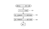
- FIG. 13B is a flowchart showing only a manufacturing process for forming a microcrystalline silicon film that will be the channel layer 30 of the TFT 210 shown in FIG. Since steps other than step S30 shown in FIG. 2 are the same in the manufacturing process of the TFT 210, the description thereof is omitted.
- a second microcrystalline silicon film 37 having a thickness of 20 nm is formed on a first microcrystalline silicon film 36 having a thickness of 50 nm including the base film. It is comprised by the laminated film laminated
- the microcrystalline silicon film is formed by a precoat process (step S31), an argon / hydrogen plasma process (step S32), and a first microcrystalline silicon film 36. (Step S33) and a step of forming a second microcrystalline silicon film 37 on the first microcrystalline silicon film 36 (Step S34).
- the Raman peak intensity ratio Ic / Ia on the first microcrystalline silicon film 36 is 8.3, and the Raman peak intensity ratio Ic / I on the second microcrystalline silicon film 37 is.
- Ia is 4.6.
- the mobility of the TFT 210 was 1.1 cm 2 / Vsec. It can be seen that this mobility is very large as compared with the mobility of the TFT 110 according to the first comparative example, which is 0.4 cm 2 / Vsec. This is considered to be because the first microcrystalline silicon film 36 is formed on the channel layer 30 of the TFT 210 on the side close to the gate electrode 20.
- a second microcrystalline silicon film 37 containing a large amount of an amorphous component is formed so as to cover the first microcrystalline silicon film 36 having a high crystallization rate.
- the second microcrystalline silicon film 37 can be removed without causing film peeling, the second microcrystalline silicon film 37, the etching stopper layer 40, and Adhesion with the ohmic contact layers 50a and 50b can be improved. Thereby, the reliability of the TFT 210 can be increased.
- FIG. 14 is a cross-sectional view showing a configuration of a TFT 220 according to a modification of the first embodiment. As shown in FIG. 14, unlike the TFT 210, no etching stopper layer is formed on the surface of the channel layer 30 of the TFT 220.
- N + The TFT 220 having a high mobility can be manufactured without peeling off the silicon film. Since the TFT 220 has the same configuration as the TFT 210 shown in FIG. 13A except that no etching stopper layer is provided, the same reference numerals as those of the TFT 210 are used and description thereof is omitted.
- the TFT 210 according to the first embodiment has been described as an n-channel TFT.
- a p-channel TFT may be formed by doping the ohmic contact layers 50a and 50b with p-type impurities at a high concentration.
- not providing an etching stopper layer or being a p-channel type can be similarly applied to the TFTs according to the second and third embodiments described later.
- FIG. 15 is a flowchart showing only steps unique to the manufacturing process of the TFT 230 in the flowchart showing the manufacturing process shown in FIG. Since steps other than step S30 shown in FIG. 2 are the same in the manufacturing process of the TFT 230, the description thereof is omitted.
- the microcrystalline silicon film is formed by argon / hydrogen plasma treatment (step S32), the first microcrystalline silicon film 36 is formed (step S33), and the first microcrystalline silicon film is formed.
- a step (step S34) of forming a second microcrystalline silicon film 37 on the crystalline silicon film 36 is included.
- the film forming process of the microcrystalline silicon film according to the present embodiment does not include the precoat process (step S31) included in the first embodiment.
- the Raman peak intensity ratio Ic / Ia on the first microcrystalline silicon film 36 is 7.7
- the second microcrystalline silicon film 37 containing a large amount of amorphous silicon is formed on the surface of the first microcrystalline silicon film 36 having a high crystallization rate.
- the chemical resistance of the channel layer 30 with respect to the hydrofluoric acid aqueous solution is 180 seconds or more, and film peeling does not occur.
- the mobility of the TFT 230 was 0.8 cm 2 / Vsec, which was larger than the mobility of the TFT 110 according to the first comparative example, which was 0.4 cm 2 / Vsec.
- the TFT 230 since the natural oxide film formed on the surface of the second microcrystalline silicon film 37 can be removed, the reliability of the TFT 230 can be increased.
- the mobility of the TFT 230 is smaller than the mobility of the TFT 210 according to the first embodiment.
- the mobility of the TFT 230 is reduced because the pre-coating process (step S31) for covering the inner wall of the chamber with the silicon film before carrying the glass substrate 15 into the chamber was not performed. This is considered to be because the residual foreign matter adhering to the inner wall of the chamber was mixed into the first or second microcrystalline silicon films 36 and 37 during the formation of the microcrystalline silicon films 36 and 37. Therefore, by providing the precoat treatment, the residual foreign matter attached to the inner wall of the chamber is less likely to be mixed into the microcrystalline silicon film 31, and the decrease in mobility of the TFT 10 due to the residual foreign matter can be suppressed. From this, it can be seen that it is preferable to provide a pre-coating treatment in the step of forming the microcrystalline silicon film 31 shown in step S30.
- FIG. 16 is a flowchart showing only steps specific to the manufacturing process of the TFT 240 in the flowchart showing the manufacturing process shown in FIG. Since steps other than step S30 shown in FIG. 2 are the same in the manufacturing process of the TFT 240, the description thereof is omitted.
- the microcrystalline silicon film is formed by a pre-coating process (step S31), a first microcrystalline silicon film 36 (step S33), and a first microcrystalline silicon film 36.
- a step (step S34) of forming a second microcrystalline silicon film 37 thereon is included.
- the film forming process of the present embodiment does not include the argon / hydrogen plasma process (step S32) included in the first embodiment.
- the Raman peak intensity ratio Ic / Ia on the first microcrystalline silicon film 36 is 6.9
- the Raman peak intensity ratio Ic / I on the second microcrystalline silicon film 37 is. Ia is 3.5.
- the second microcrystalline silicon film 37 containing a large amount of amorphous silicon is formed on the surface of the first microcrystalline silicon film 36 having high crystallinity.
- the chemical resistance of the channel layer 30 to the hydrofluoric acid aqueous solution is 180 seconds or more, and no film peeling occurs.
- the channel layer of the TFT 240 has a configuration in which the order of stacking the first microcrystalline silicon film 36 and the second microcrystalline silicon film constituting the channel layer of the TFT 130 shown in FIG. 9A is reversed.
- the chemical resistance is very different. This is because the ease of film peeling is not determined only by the immersion time in the chemical solution, but by changing the stacking order, the surface state of the lower microcrystalline silicon film changes, and accordingly the upper microcrystalline This is because the ease of peeling of the silicon film also changes.
- the mobility of the TFT240 is 0.7 cm 2 / Vsec, increased as compared to 0.4 cm 2 / Vsec is a mobility of TFT110 according to the first comparative example.
- the TFT 240 film peeling does not occur and the mobility increases.
- the reliability of the TFT 240 can be increased.
- the mobility of the TFT 240 is smaller than the mobility of the TFT 210 according to the first embodiment.
- the mobility of the TFT 240 is thus reduced because the argon / hydrogen plasma treatment (step S32) for cleaning the surface of the gate insulating film 25 and forming a thin microcrystalline silicon film was not performed. This is probably because a thin amorphous silicon film was formed on the surface of the film 25. Therefore, by providing the argon / hydrogen plasma treatment, it is difficult for the incubation film to grow on the surface of the gate insulating film 25, and a decrease in mobility of the TFT 240 can be suppressed. From this, it can be seen that it is preferable to provide argon / hydrogen plasma treatment in the step of forming the microcrystalline silicon film 31 shown in step S30.
- step S30 shown in FIG. 2 includes at least one of pre-coating processing and argon / hydrogen plasma processing.
- step S30 may not include any of the precoat process and the argon / hydrogen plasma process.
- the crystallization rate of the first microcrystalline silicon film 36 is low, the mobility of the TFT is low compared to the cases of the first to third embodiments.
- the mobility is 0.7 cm 2 / Vsec or more and the chemical resistance to the hydrofluoric acid aqueous solution is 180 seconds or more. Therefore, as can be seen from FIG. 12, the Raman peak intensity ratio Ic / Ia of the first microcrystalline silicon film 36 is set to 7.0 or higher, preferably 7.5 or higher, and the Raman peak of the second microcrystalline silicon film 37 is increased.
- the intensity ratio Ic / Ia is 4.5 or less, preferably 4.0 or less.
- the pressure (first pressure value) at the time of forming the first microcrystalline silicon film 36 is set to 20 mTorr or more, preferably 23 mTorr or more, and the pressure at the time of forming the second microcrystalline silicon film 37 (second pressure).
- the pressure value is 5 mTorr or less.
- the ratio of the crystal component in the microcrystalline silicon film which greatly affects the mobility and chemical resistance is determined depending on the pressure in the chamber when the microcrystalline silicon film is formed. That is, the higher the pressure in the chamber, the higher the crystallization rate of the microcrystalline silicon film. From this, the pressure (first pressure value) when forming the first microcrystalline silicon film is at least higher than the pressure (second pressure value) when forming the second microcrystalline silicon film. It can be seen that the first microcrystalline silicon film may be formed under such a condition that the height of the first microcrystalline silicon film increases. The Raman peak intensity ratio Ic / Ia of the first microcrystalline silicon film formed under such conditions is larger than the Raman peak intensity ratio Ic / Ia of the second microcrystalline silicon film.
- the first pressure value is set to 40 mTorr or more, and the second pressure It can be seen that the value should be 5 mTorr or less.
- FIG. 17 is a block diagram showing a configuration of the liquid crystal display device 1 including any of the TFTs 210 to 240 according to the first to third embodiments.
- a liquid crystal display device 1 shown in FIG. 17 includes a liquid crystal panel 2, a display control circuit 3, a gate driver 4, and a source driver 5.
- the liquid crystal panel 2 includes n (n is an integer of 1 or more) gate wirings G1 to Gn extending in the horizontal direction and m (m is an integer of 1 or more) extending in a direction intersecting the gate wirings G1 to Gn.
- Source wirings S1 to Sm are formed.
- Pixel forming portions Pij are arranged near intersections of the i-th gate line Gi (i is an integer of 1 to n) and the j-th source line Sj (j is an integer of 1 to m). .
- the display control circuit 3 is supplied with a control signal SC such as a horizontal synchronizing signal and a vertical synchronizing signal and an image signal DT from the outside of the liquid crystal display device 1. Based on these signals, the display control circuit 3 outputs a control signal SC1 to the gate driver 4, and outputs a control signal SC2 and an image signal DT to the source driver 5.
- a control signal SC such as a horizontal synchronizing signal and a vertical synchronizing signal and an image signal DT
- the gate driver 4 is connected to the gate lines G1 to Gn, and the source driver 5 is connected to the source lines S1 to Sm.
- the gate driver 4 sequentially applies a high level signal indicating the selected state to the gate lines G1 to Gn.
- the gate wirings G1 to Gn are sequentially selected one by one. For example, when the i-th gate line Gi is selected, the pixel formation portions Pi1 to Pim for one row are selected at once.
- the source driver 5 applies a signal voltage corresponding to the image signal DT to each of the source lines S1 to Sm. As a result, the signal voltage corresponding to the image signal DT is written into the pixel formation portions Pi1 to Pim for one selected row. In this way, the liquid crystal display device 1 displays an image on the liquid crystal panel 2.
- the liquid crystal panel 2 is sometimes referred to as a “display unit”, and the gate driver 4 and the source driver 5 may be collectively referred to as a “drive circuit”.
- FIG. 18 is a plan view showing a pattern arrangement in the pixel formation portion Pij provided in the liquid crystal panel 2.
- the liquid crystal panel 2 is surrounded by an i-th gate line Gi extending in the horizontal direction, a j-th source line Sj extending in a direction intersecting the gate line Gi, the gate line Gi, and the source line Sj.
- a pixel forming portion Pij disposed in the region.
- the pixel formation portion Pij includes a TFT 210 shown in FIG. 13A as a TFT that functions as a switching element.
- the gate electrode 20 of the TFT 210 is electrically connected to the gate wiring Gi.
- an island-shaped channel layer 30 extending left and right across the gate electrode 20 is formed.
- the left end of the channel layer 30 is electrically connected to the source electrode connected to the source wiring Sj, and the right end of the channel layer 30 is electrically connected to the drain electrode. Further, the drain electrode is connected to the pixel electrode 7 through the contact hole 6.
- the pixel electrode 7 and a counter electrode constitute a pixel capacitor that holds a signal voltage corresponding to the image signal DT for a predetermined time.
- FIG. 19 is a cross-sectional view of the TFT 210 that functions as a switching element of the pixel formation portion Pij of the liquid crystal display device 1.
- FIG. 19 is a cross-sectional view showing that the pixel electrode 7 is connected to the drain electrode 60b of the TFT 210 shown in FIG. 13A.
- the same reference numerals are given to the same components as those of the TFT 210, and The description is omitted.
- the planarization film 8 is formed on the surface of the passivation film 70, and the contact hole 6 reaching the drain electrode 60 b is opened in the planarization film 8.
- a pixel electrode 7 made of a transparent metal such as ITO (Indium Tin Oxide) is formed on the surface of the planarizing film 8, and the pixel electrode 7 is electrically connected to the drain electrode 60 b through the contact hole 6. ing.
- the gate electrode 20 is connected to any one of the gate lines G1 to Gn, and the source electrode 60a is connected to any one of the source lines S1 to Sm.
- the TFT 210 As described above, if the TFT 210 according to the present embodiment is used as a switching element of each pixel formation portion Pij provided in the liquid crystal panel 2, the mobility is increased. In this case, since the TFT 210 can charge the pixel capacitor with the signal voltage of the image signal supplied from the source wiring Sj in a short time, the number of pixel formation portions Pij can be increased to achieve high definition. Further, since the chemical resistance of the channel layer 30 of the TFT 210 is improved, the liquid crystal panel 2 including the pixel formation portion Pij can be easily formed.
- the gate driver 4 and the source driver 5 can be configured on the frame of the liquid crystal panel 2 using the TFT 210 according to the present embodiment.
- the on-current of the TFT 210 is large, the operation speed of the gate driver 4 and the source driver 5 is increased, and a high frame rate can be realized.
- the circuit scale of the gate driver 4 and the source driver 5 can be reduced, the frame of the liquid crystal panel 2 can be reduced, and the power consumption of the liquid crystal display device 1 can be reduced.
- the chemical resistance of the channel layer 30 of the TFT 210 is improved, the reliability of the TFT 210 is improved, and as a result, the reliability of the gate driver 4 and the source driver 5 is improved.
- FIGS. 18 and 19 have described the case where the TFT 210 is used as the switching element of each pixel formation portion Pij, any of the TFTs 220 to 240 may be used instead of the TFT 210.
- the present invention can also be applied to an organic EL (Electro-Luminescence) display device.
- the present invention is suitable for a thin film transistor used in a display device such as an active matrix liquid crystal display device, and in particular, a switching element formed in the pixel formation portion or a transistor of a drive circuit for driving the pixel formation portion. Suitable for
Landscapes
- Thin Film Transistor (AREA)
Abstract
移動度を大きく保った状態で、薬液耐性が高いチャネル層を有する薄膜トランジスタおよびその製造方法を提供する。 TFT(210)のチャネル層(30)は、高密度プラズマCVD装置により、ゲート絶縁膜(25)上に成膜された第1の微結晶シリコン膜(36)と、第1の微結晶シリコン膜(36)の成膜時の圧力よりも低い圧力で第1の微結晶シリコン膜(36)上に成膜された第2の微結晶シリコン膜(37)によって構成されている。第1の微結晶シリコン膜(36)は柱状に成長した結晶粒を多く含むので、TFT(210)の移動度が大きくなる。また、第2の微結晶シリコン膜(37)は非晶質成分を多く含むので、チャネル層(30)の表面に形成された自然酸化膜を除去する際に、チャネル層(30)を薬液に浸漬しても、チャネル層(30)の膜剥がれは生じにくい。
Description
本発明は、薄膜トランジスタおよびその製造方法、並びに表示装置に関し、特に、微結晶半導体膜を用いた薄膜トランジスタおよびその製造方法、並びに表示装置に関する。
アクティブマトリクス型液晶表示装置において、画素形成部のスイッチング素子や、駆動回路を構成する半導体素子として薄膜トランジスタ(Thin Film Transistor:以下、「TFT」と略す)が用いられている。このようなTFTのチャネル層には、従来、非晶質シリコン膜または多結晶シリコン膜が使用されていた。しかし、近年、非晶質シリコン膜よりも移動度が大きく、また多結晶シリコン膜のようにアニール処理を必要としない微結晶シリコン膜が使用されるようになってきた。
例えば、特許文献1では、逆スタガード型TFTのチャネル層として、まずゲート絶縁膜上に、シランガス(SiH4)の希釈倍率を大きくすることによって成膜速度を遅くした第1の微結晶シリコン膜を形成する。次に、第1の微結晶シリコン膜上に、シランガスの希釈倍率を小さくすることによって成膜速度を速くした第2の微結晶シリコン膜を形成する。これにより、ゲート電極に近い第1の微結晶シリコン膜の結晶性を第2の微結晶シリコン膜の結晶性よりも高くして、TFTの移動度を向上させている。
TFTを製造するには、第2の微結晶シリコン膜上に、エッチングストッパ層を形成したり、オーミックコンタクト層を形成したりする必要がある。これらの層と第2の微結晶シリコン膜との密着性を良くするために、第2の微結晶シリコン膜の表面に形成されている自然酸化膜をあらかじめ除去しておくことが好ましい。自然酸化膜の除去には、例えばフッ酸(HF)の濃度を5%とした水溶液(以下、「フッ酸水溶液」という)等のフッ酸系の薬液が用いられる。
一般に微結晶シリコン膜は、結晶粒が基板に垂直な方向に成長した柱状結晶になり、水平方向の物理的結合が弱くなっている。そこで、第2の微結晶シリコン膜の表面に形成されている自然酸化膜を除去するために、第2の微結晶シリコン膜をフッ酸水溶液に浸漬すれば、フッ酸水溶液は第2の微結晶シリコン膜の表面から結晶粒界に沿って第1の微結晶シリコン膜内に侵入し、ゲート絶縁膜をエッチングする。ゲート絶縁膜のエッチングが進めば、第1および第2の微結晶シリコン膜はリフトオフされて膜剥がれが生じる。膜剥がれが生じればチャネル層は形成されず、TFTを製造することができない。
しかし、特許文献1では、シランガスの希釈倍率を変えて、第2の微結晶シリコン膜のラマンピーク強度比を3.52にしたり、6.19にしたりすることが記載されている。このことから、特許文献1では、第2の微結晶シリコン膜の結晶性を、第1の微結晶シリコン膜の結晶性よりも低くすることだけを目的とし、自然酸化膜をフッ酸水溶液によって除去したときに生じる膜剥がれについては考慮されていない。このため、特許文献1には、フッ酸水溶液に対する耐性を高くして膜剥がれを防止する解決方法は開示されていない。
そこで、本発明の目的は、移動度を大きくした状態で、薬液耐性が高いチャネル層を有する薄膜トランジスタおよびその製造方法を提供することである。また、本発明の他の目的は、そのような薄膜トランジスタを用いて高精細化およびハイフレームレート化が可能な表示装置を提供することである。
本発明の第1の局面は、絶縁基板上に形成された薄膜トランジスタであって、
前記絶縁基板上に形成されたゲート電極と、
前記ゲート電極を覆うように形成されたゲート絶縁膜と、
前記ゲート絶縁膜上に形成されたチャネル層とを備え、
前記チャネル層は、
前記ゲート絶縁膜の表面に形成され、ラマンピーク強度比が7.0以上である第1の微結晶半導体膜と、
前記第1の微結晶半導体膜の表面に形成され、ラマンピーク強度比が4.5以下である第2の微結晶半導体膜とを含むことを特徴とする。
前記絶縁基板上に形成されたゲート電極と、
前記ゲート電極を覆うように形成されたゲート絶縁膜と、
前記ゲート絶縁膜上に形成されたチャネル層とを備え、
前記チャネル層は、
前記ゲート絶縁膜の表面に形成され、ラマンピーク強度比が7.0以上である第1の微結晶半導体膜と、
前記第1の微結晶半導体膜の表面に形成され、ラマンピーク強度比が4.5以下である第2の微結晶半導体膜とを含むことを特徴とする。
本発明の第2の局面は、本発明の第1の局面において、
前記ゲート絶縁膜の表面上に、前記第1の微結晶半導体膜の下地膜になる第3の微結晶半導体膜が形成されていることを特徴とする。
前記ゲート絶縁膜の表面上に、前記第1の微結晶半導体膜の下地膜になる第3の微結晶半導体膜が形成されていることを特徴とする。
本発明の第3の局面は、本発明の第1の局面において、
前記チャネル層の表面上に形成されたエッチングストッパ層をさらに備えていることを特徴とする。
前記チャネル層の表面上に形成されたエッチングストッパ層をさらに備えていることを特徴とする。
本発明の第4の局面は、絶縁基板上に形成された薄膜トランジスタの製造方法であって、
前記絶縁基板上にゲート電極を形成する工程と、
前記ゲート電極を覆うようにゲート絶縁膜を成膜する工程と、
前記ゲート絶縁膜上に高密度プラズマCVD装置内でチャネル層を形成する工程とを備え、
前記チャネル層を形成する工程は、
前記高密度プラズマCVD装置内の圧力を第1の圧力値にして、第1の微結晶半導体膜を成膜する工程と、
前記高密度プラズマCVD装置内の圧力を前記第1の圧力値よりも低い第2の圧力値にして、第2の微結晶半導体膜を成膜する工程とを含むことを特徴とする。
前記絶縁基板上にゲート電極を形成する工程と、
前記ゲート電極を覆うようにゲート絶縁膜を成膜する工程と、
前記ゲート絶縁膜上に高密度プラズマCVD装置内でチャネル層を形成する工程とを備え、
前記チャネル層を形成する工程は、
前記高密度プラズマCVD装置内の圧力を第1の圧力値にして、第1の微結晶半導体膜を成膜する工程と、
前記高密度プラズマCVD装置内の圧力を前記第1の圧力値よりも低い第2の圧力値にして、第2の微結晶半導体膜を成膜する工程とを含むことを特徴とする。
本発明の第5の局面は、本発明の第4の局面において、
前記チャネル層を形成する工程は、前記絶縁基板を前記高密度プラズマCVD装置内に搬入する前に、前記高密度プラズマCVD装置の内壁を半導体膜で覆う処理をさらに含むことを特徴とする。
前記チャネル層を形成する工程は、前記絶縁基板を前記高密度プラズマCVD装置内に搬入する前に、前記高密度プラズマCVD装置の内壁を半導体膜で覆う処理をさらに含むことを特徴とする。
本発明の第6の局面は、本発明の第4または第5の局面において、
前記チャネル層を形成する工程は、前記高密度プラズマCVD装置の内壁を半導体膜で覆う工程の後であって、前記第1の微結晶半導体膜を成膜する工程の前に、アルゴンガスおよび水素ガスのプラズマによって前記ゲート絶縁膜の表面を清浄にし、前記第1の微結晶シリコン膜の下地膜になる第3の微結晶半導体膜を前記ゲート絶縁膜の表面に成膜する処理をさらに含むことを特徴とする。
前記チャネル層を形成する工程は、前記高密度プラズマCVD装置の内壁を半導体膜で覆う工程の後であって、前記第1の微結晶半導体膜を成膜する工程の前に、アルゴンガスおよび水素ガスのプラズマによって前記ゲート絶縁膜の表面を清浄にし、前記第1の微結晶シリコン膜の下地膜になる第3の微結晶半導体膜を前記ゲート絶縁膜の表面に成膜する処理をさらに含むことを特徴とする。
本発明の第7の局面は、本発明の第6の局面において、
前記第3の微結晶半導体膜の膜厚は、3~7nmであることを特徴とする。
前記第3の微結晶半導体膜の膜厚は、3~7nmであることを特徴とする。
本発明の第8の局面は、本発明の第4の局面において、
前記第1の圧力値は20mTorr以上であり、前記第2の圧力値は5mTorr以下であることを特徴とする。
前記第1の圧力値は20mTorr以上であり、前記第2の圧力値は5mTorr以下であることを特徴とする。
本発明の第9の局面は、画像を表示するアクティブマトリクス型の表示装置であって、
複数のゲート配線と、前記複数のゲート配線と交差する複数のソース配線と、前記複数のゲート配線と前記複数のソース配線との交差点にそれぞれ対応してマトリクス状に配置された複数の画素形成部とを備える表示部と、
前記複数の画素形成部を駆動する駆動回路とを備え、
前記画素形成部は、対応するゲート配線に印加される信号に応じてオンまたはオフするスイッチング素子を含み、
前記スイッチング素子は、第1の局面に係る薄膜トランジスタを含むことを特徴とする。
複数のゲート配線と、前記複数のゲート配線と交差する複数のソース配線と、前記複数のゲート配線と前記複数のソース配線との交差点にそれぞれ対応してマトリクス状に配置された複数の画素形成部とを備える表示部と、
前記複数の画素形成部を駆動する駆動回路とを備え、
前記画素形成部は、対応するゲート配線に印加される信号に応じてオンまたはオフするスイッチング素子を含み、
前記スイッチング素子は、第1の局面に係る薄膜トランジスタを含むことを特徴とする。
本発明の第10の局面は、本発明の第9の局面において、
前記駆動回路は、本発明の第9の局面に係る薄膜トランジスタによって構成されていることを特徴とする。
前記駆動回路は、本発明の第9の局面に係る薄膜トランジスタによって構成されていることを特徴とする。
上記第1の局面によれば、薄膜トランジスタのチャネル層は、ゲート絶縁膜上に形成された第1の微結晶半導体膜と、第1の微結晶半導体膜上に形成された第2の微結晶半導体膜とを含む。第1の微結晶半導体膜は、ラマンピーク強度比が7.0以上であるので、結晶粒が柱状に成長している。これにより、薄膜トランジスタの移動度を0.7cm2/Vsec以上にすることができる。また、第2の微結晶半導体膜は、ラマンピーク強度比が4.5以下であるので、非晶質成分が多く含むとともに、第1の微結晶半導体膜を覆っている。そこで、チャネル層を薬液に浸漬しても、薬液は第1の微結晶半導体膜内に侵入しにくい。これにより、チャネル層のフッ酸水溶液に対する薬液耐性を180秒以上にすることができる。このように、薄膜トランジスタでは、移動度を高く保った状態で、薬液耐性が向上する。
上記第2の局面によれば、ゲート絶縁膜の表面上に、第3の微結晶半導体膜を形成することにより、ゲート絶縁膜上にインキュベーション層が成長しにくくなる。これにより、第3の微結晶シリコン膜を下地膜として成膜する第1の微結晶シリコン膜の結晶性が高くなり、薄膜トランジスタの移動度を高く保つことができる。
上記第3の局面によれば、表面にエッチングストッパ層が形成されたチャネル層を薬液に浸漬しても、膜剥がれが生じることなく、チャネル層の表面に形成されている自然酸化膜を除去することができる。これにより、チャネル層とエッチングストッパ層との密着性を良くすることができる。
上記第4の局面によれば、高密度プラズマCVD装置内の圧力を第1の圧力値にして、第1の微結晶半導体膜を成膜した後に、第2の微結晶半導体膜を、第1の圧力値よりも低い第2の圧力値にして成膜する。第1の微結晶半導体膜では、結晶粒が柱状に成長するので、薄膜トランジスタの移動度が大きくなる。また、第2の微結晶半導体膜には非晶質成分が多く含まれているので、チャネル層を薬液に浸漬しても、薬液は第2の微結晶半導体膜によって覆われた第1の微結晶半導体膜内に侵入しにくくなる。これにより、移動度を高く保った状態で、薬液耐性が向上した薄膜トランジスタを製造することができる。また、高密度プラズマCVD装置内の圧力を変えることにより第1および第2の微結晶シリコン膜の結晶性を制御するので、結晶性を精度よく制御することができる。
上記第5の局面によれば、絶縁基板を高密度プラズマCVD装置内に搬入する前に、高密度プラズマCVD装置の内壁を半導体膜で覆う。これにより、第1または第2の微結晶シリコン膜の成膜時に、高密度プラズマCVD装置の内壁に付着していた残留異物が、第1または第2の微結晶半導体膜内に混入して薄膜トランジスタの移動度を低下させることを抑制することができる。
上記第6の局面によれば、ゲート絶縁膜上に吸着された水分、有機物、金属粒子等が除去されて、ゲート絶縁膜の表面が清浄にされる。これにより、ゲート絶縁膜の表面上にインキュベーション膜の成長をしにくくしたり、水分中の酸素原子等が第1の微結晶シリコン膜内に混入して、薄膜トランジスタの移動度を低下させたりすることを防ぐことができる。また、ゲート絶縁膜上に形成された第3の微結晶シリコン膜を下地膜として成膜する第1の微結晶シリコン膜の結晶性が高くなり、薄膜トランジスタの移動度をより高く保つことができる。
上記第7の局面によれば、第3の微結晶半導体膜の膜厚を3nmよりも薄くすれば、インキュベーション膜が成長し、その上に成膜される第1の微結晶シリコン膜の結晶性が低くなる。また、膜厚が7nmよりも厚くすれば、第3の微結晶シリコン膜の形成時間が長くなる。そこで、第3の微結晶半導体膜の膜厚を3~7nmにすれば、これらの問題点がなくなる。
上記第8の局面によれば、第1の微結晶半導体膜を成膜する際の第1の圧力値を20mTorr以上にすることにより、薄膜トランジスタの移動度を0.7cm2/Vsec以上にすることができる。また、第2の微結晶半導体膜を成膜する際の第2の圧力値を5mTorr以下にすることにより、第2の微結晶半導体膜によって覆われた第1の半導体膜内にフッ酸水溶液が侵入しにくくなるので、薬液耐性を180秒以上にすることができる。
上記第9の局面によれば、画素形成部のスイッチング素子として、第1の局面に係る薄膜トランジスタを用いれば、薄膜トランジスタに流れるオン電流は大きくなる。この場合、薄膜トランジスタは、画像信号の信号電圧を、短時間で画素容量に充電できるので、画素形成部の数を増やして高精細化を図ることが可能になる。また、薄膜トランジスタの薬液耐性が向上するので、画素形成部を含む表示部の形成が容易になる。
上記第10の局面によれば、第1の局面に係る薄膜トランジスタに流れるオン電流は大きい。この場合、第1の局面に係る薄膜トランジスタを用いて駆動回路を構成すれば、駆動回路の動作速度が速くなり、ハイフレームレート化しやすくなる。また、駆動回路の回路規模を小さくすることができるので、表示部の額縁を小さくすることができるとともに、表示装置の低消費電力化を図ることができる。さらに、薄膜トランジスタの薬液耐性が向上するので、信頼性が高い駆動回路を形成することができる。
<1.TFTの構成>
図1は、逆スタガード型TFT10の構成を示す断面図である。図1を参照して、TFT10の構成を説明する。絶縁基板であるガラス基板15上に、膜厚100nmのチタン(Ti)膜からなるゲート電極20が形成されている。ゲート電極20を含むガラス基板15の全体を覆うように、窒化シリコン膜(SiNx)からなるゲート絶縁膜25が形成されている。ゲート絶縁膜25の膜厚は、例えば410nmである。
図1は、逆スタガード型TFT10の構成を示す断面図である。図1を参照して、TFT10の構成を説明する。絶縁基板であるガラス基板15上に、膜厚100nmのチタン(Ti)膜からなるゲート電極20が形成されている。ゲート電極20を含むガラス基板15の全体を覆うように、窒化シリコン膜(SiNx)からなるゲート絶縁膜25が形成されている。ゲート絶縁膜25の膜厚は、例えば410nmである。
ゲート絶縁膜25の表面に、平面視においてゲート電極20を跨いで左右に延びる島状のチャネル層30が形成されている。チャネル層30の膜厚は、例えば70nmである。チャネル層30は、不純物を含まない微結晶シリコン膜からなる。チャネル層30の具体的な構成は、後述する比較例および実施形態ごとに異なる。ゲート電極20と対向するチャネル層30の表面には、窒化シリコン膜からなるエッチングストッパ層40が形成されている。エッチングストッパ層40の膜厚は、例えば150nmである。
エッチングストッパ層40の左上面からチャネル層30の左端までを覆うように延在するオーミックコンタクト層50aと、エッチングストッパ層40の右上面からチャネル層30の右端までを覆うように延在するオーミックコンタクト層50bが形成されている。これらのオーミックコンタクト層50a、50bは、リン(P)等のn型不純物を高濃度にドープした微結晶シリコン膜(n+シリコン膜)からなり、エッチングストッパ層40の上面で左右に分離されている。
オーミックコンタクト層50aの右端上面からオーミックコンタクト層50aを覆って左側のゲート絶縁膜25上まで延在するソース電極60aと、オーミックコンタクト層50bの左端上面からオーミックコンタクト層50bを覆って右側のゲート絶縁膜25上まで延在するドレイン電極60bとが形成されている。ソース電極60aはオーミックコンタクト層50aを介してチャネル層30とオーミック接触し、ドレイン電極60bはオーミックコンタクト層50bを介してチャネル層30とオーミック接触している。さらに、ソース電極60aとドレイン電極60bを含むガラス基板15の全体を覆うように、窒化シリコン膜からなるパッシベーション膜70が形成されている。
<1.1 TFTの製造方法>
図2は、図1に示すTFT10を製造するためのプロセスフローを示すフロー図である。また、図3(a)~図3(c)、図4(a)~図4(c)、図5(a)および図5(b)は、図1に示すTFT10の各製造工程を示す断面図である。図2に示すプロセスフロー、並びに、図3(a)~図3(c)、図4(a)~図4(c)、図5(a)および図5(b)に示す各断面図を参照して、TFT10の製造工程を説明する。
図2は、図1に示すTFT10を製造するためのプロセスフローを示すフロー図である。また、図3(a)~図3(c)、図4(a)~図4(c)、図5(a)および図5(b)は、図1に示すTFT10の各製造工程を示す断面図である。図2に示すプロセスフロー、並びに、図3(a)~図3(c)、図4(a)~図4(c)、図5(a)および図5(b)に示す各断面図を参照して、TFT10の製造工程を説明する。
ステップS10では、ガラス基板15上に例えばチタン膜またはチタンを主成分とする金属膜をスパッタリング法によって成膜する。チタン膜の膜厚は、例えば100nmである。なお、チタン膜の代わりに、タングステン(W)、モリブデン(Mo)、アルミニウム(Al)等の金属膜、それらを主成分とする金属膜、またはそれらを積層した金属膜を成膜してもよい。
次に、チタン膜の表面に、フォトリソグラフィ法を用いてレジストパターンを形成する。図3(a)に示すように、レジストパターン(図示しない)をマスクにして、チタン膜をウエットエッチング法によりエッチングし、ゲート電極20を形成する。その後、レジストパターンを剥離する。なお、ウエットエッチング法の代わりに、ドライエッチング法によりエッチングしてゲート電極20を形成してもよい。
ステップS20では、図3(b)に示すように、ゲート電極20を含むガラス基板15の全体を覆うように、平行平板化学気相成長(Chemical Vapor Deposition:以下、「平行平板CVD」という)装置により、シランガスと窒素ガス(N2)を含む原料ガスからゲート絶縁膜25となる窒化シリコン膜を成膜する。窒化シリコン膜の膜厚は、例えば410nmである。なお、ゲート絶縁膜25として、窒化シリコン膜の代わりに酸化シリコン(SiO2)膜、酸窒化シリコン(SiON)膜、またはそれらの積層膜を成膜してもよい。
ステップS30では、図3(c)に示すように、ゲート絶縁膜25の表面に、複数層からなる微結晶シリコン膜31を成膜する。微結晶シリコン膜31は、表面波プラズマ方式またはICP(Inductively Coupled Plasma:誘導結合プラズマ)方式等の高密度プラズマCVD装置を用いて成膜される。微結晶シリコン膜31の膜厚は、例えば70nmである。なお、微結晶シリコン膜31に含まれる複数層の構成および成膜条件は比較例および実施形態ごとに異なるので、それらについては後述する。
ステップS40では、微結晶シリコン膜31の表面に形成されている自然酸化膜を除去する。具体的には、微結晶シリコン膜31を薄い酸系の溶液に40秒間浸漬し、その後水洗して乾燥させる。これにより、微結晶シリコン膜31の表面に形成されていた自然酸化膜が除去される。微結晶シリコン膜31を浸漬する薄い酸系の水溶液として、例えばフッ酸の濃度が0.5%のフッ酸水溶液、バッファードフッ酸等を使用する。このように、エッチングストッパ層40となる窒化シリコン膜を成膜する前に自然酸化膜を除去するのは以下の理由による。すなわち、自然酸化膜を除去しないで、微結晶シリコン膜31の表面に後述する窒化シリコン膜41を成膜すれば、微結晶シリコン膜31と窒化シリコン膜41との密着性が悪くなり、エッチングストッパ層40が剥がれやすくなるからである。
ステップS50では、図4(a)に示すように、自然酸化膜を除去した直後のガラス基板15を平行平板CVD装置内に搬入し、シランガスとアンモニアガス(NH3)を含む原料ガスを用いて微結晶シリコン膜31の表面に窒化シリコン膜41を成膜する。窒化シリコン膜41の膜厚は例えば150nmである。窒化シリコン膜41の表面上であって、ゲート電極20と対向する位置に、フォトリソグラフィ法によってレジストパターン45を形成する。レジストパターン45をマスクにして、窒化シリコン膜41をドライエッチング法によりエッチングし、エッチングストッパ層40を形成する。なお、エッチングストッパ層40は、酸化シリコン膜または酸窒化シリコン膜をエッチングして形成してもよい。
ステップS60では、エッチングストッパ層40で覆われていない微結晶シリコン膜31の表面に形成されている自然酸化膜を除去する。自然酸化膜の除去方法は、ステップS40における自然酸化膜の除去と同じであるので、その説明を省略する。なお、微結晶シリコン膜31をフッ酸水溶液に浸漬する時間は20秒間である。このように、自然酸化膜を除去するのは、微結晶シリコン膜31の表面に形成されている自然酸化膜を除去しないで、微結晶シリコン膜31の表面に後述する非晶質シリコン膜51を成膜すれば、微結晶シリコン膜31と非晶質シリコン膜51との密着性が悪くなり、オーミックコンタクト層50a、50bが剥がれやすくなるからである。
ステップS70では、図4(b)に示すように、エッチングストッパ層40および微結晶シリコン膜31を含むガラス基板15の全体を覆うように、オーミックコンタクト層50a、50bとなる非晶質シリコン膜51を成膜する。非晶質シリコン膜51は、ソース電極60aおよびドレイン電極60bがチャネル層30とオーミック接触するように、例えばリン(P)等のn型不純物が高濃度にドープされた非晶質シリコン膜(以下、「n+シリコン膜51」という)である。
ステップS80では、図4(c)に示すように、n+シリコン膜51の表面に、フォトリソグラフィ技術を用いてレジストパターン55を形成する。レジストパターン55をマスクにして、ドライエッチング法により、n+シリコン膜51と微結晶シリコン膜31とを連続してエッチングする。その後、レジストパターン55を剥離する。これにより、島状のチャネル層30が形成されるとともに、n+シリコン膜51はチャネル層30と同じ形状になる。
ステップS90では、図5(a)に示すように、スパッタリング装置を用いてソースメタル膜61を成膜する。ソースメタル膜61は、例えばチタン膜またはチタンを主成分とする金属膜である。ソースメタル膜61上に、フォトリソグラフィ法を用いて、エッチングストッパ層40の上方に開口部を有するレジストパターン65を形成する。
次に、図5(b)に示すように、レジストパターン65をマスクにして、ウエットエッチング法によりソースメタル膜61をエッチングし、ソース電極60aおよびドレイン電極60bを形成する。なお、ウエットエッチング法の代わりにドライエッチング法によって、ソースメタル膜61をエッチングしてもよい。
さらに、レジストパターン65をマスクにして、ドライエッチング法によりn+シリコン膜51をエッチングし、エッチングストッパ層40の上面で左右に分離された2つのオーミックコンタクト層50a、50bを形成する。なお、チャネル層30の上面に、窒化シリコンからなるエッチングストッパ層40が形成されているので、n+シリコン膜51のエッチングはエッチングストッパ層40によって停止し、チャネル層30の表面がエッチングされることはない。ソース電極60aは、オーミックコンタクト層50aの右端上面からオーミックコンタクト層50aを覆って左側のゲート絶縁膜25上まで延在し、ドレイン電極60bは、オーミックコンタクト層50bの左端上面からオーミックコンタクト層50bを覆って右側のゲート絶縁膜25上まで延在する。
ステップS100では、ソース電極60aとドレイン電極60bを含むガラス基板15の全体を覆うように、窒化シリコンからなるパッシベーション膜70を成膜する。パッシベーション膜70は、平行平板プラズマCVD装置により、シランガスとアンモニアガスを含む原料ガスを用いて成膜され、その膜厚は例えば265nmである。その後、ソース電極60aとオーミックコンタクト層50a、および、ドレイン電極60bとオーミックコンタクト層50bがそれぞれオーミック接触するように、TFT10を形成したガラス基板15を窒素雰囲気中において200℃で1時間加熱する。以上説明した一連の製造工程によって、図1に示すTFT10が製造される。
<1.2 微結晶シリコン膜の成膜方法>
図2のステップS30に示す微結晶シリコン膜31の成膜方法には、次の4つの処理工程が含まれる。すなわち、高密度プラズマCVD装置のチャンバの内壁をシリコン膜で被覆するプリコート処理、アルゴン・水素プラズマ処理を施すことによりゲート絶縁膜25の表面を清浄にして薄い微結晶シリコン膜を成膜するアルゴン・水素プラズマ処理、結晶性が高い第1の微結晶シリコン膜を成膜する工程、第1の微結晶シリコン膜よりも結晶性が低い第2の微結晶シリコン膜を成膜する工程が含まれている。そこで、これらの処理工程について説明する。
図2のステップS30に示す微結晶シリコン膜31の成膜方法には、次の4つの処理工程が含まれる。すなわち、高密度プラズマCVD装置のチャンバの内壁をシリコン膜で被覆するプリコート処理、アルゴン・水素プラズマ処理を施すことによりゲート絶縁膜25の表面を清浄にして薄い微結晶シリコン膜を成膜するアルゴン・水素プラズマ処理、結晶性が高い第1の微結晶シリコン膜を成膜する工程、第1の微結晶シリコン膜よりも結晶性が低い第2の微結晶シリコン膜を成膜する工程が含まれている。そこで、これらの処理工程について説明する。
<1.2.1 プリコート処理>
ガラス基板15を高密度プラズマCVD装置のチャンバ内に搬入する前に、チャンバ内にシランガスを導入してプラズマを生成し、チャンバの内壁をシリコン膜で被覆する。このようなプリコート処理を施すことにより、微結晶シリコン膜31の成膜中に、チャンバの内壁に付着していた残留異物が剥がれて微結晶シリコン膜31内に混入することが少なくなる。
ガラス基板15を高密度プラズマCVD装置のチャンバ内に搬入する前に、チャンバ内にシランガスを導入してプラズマを生成し、チャンバの内壁をシリコン膜で被覆する。このようなプリコート処理を施すことにより、微結晶シリコン膜31の成膜中に、チャンバの内壁に付着していた残留異物が剥がれて微結晶シリコン膜31内に混入することが少なくなる。
次に、プリコート処理のプロセス条件の詳細を以下に示す。なお、下記プロセス条件における「ギャップ」とは、ガラス基板15の表面と高密度プラズマCVD装置の電極の表面との間隔をいう。
マイクロ波周波数 : 915MHz
パワー : 0.8W/cm2(投入パワー:1.0kW)
圧力 : 20mTorr
ギャップ : 90mm
SiH4流量 : 400sccm
Ar流量 : 600sccm
チャンバ内温度 : 100℃
処理時間 : 600sec
マイクロ波周波数 : 915MHz
パワー : 0.8W/cm2(投入パワー:1.0kW)
圧力 : 20mTorr
ギャップ : 90mm
SiH4流量 : 400sccm
Ar流量 : 600sccm
チャンバ内温度 : 100℃
処理時間 : 600sec
<1.2.2 アルゴン・水素プラズマ処理>
微結晶シリコン膜31を成膜する際に、ゲート絶縁膜25の表面に水分、有機物、金属粒子等が吸着していれば、ゲート絶縁膜上にインキュベーション膜が形成されやすくなったり、水分中の酸素原子等が微結晶シリコン膜31内に混入したりするおそれがある。微結晶シリコン膜31にインキュベーション膜が形成されたり酸素原子等が混入したりすれば、TFT10の移動度が低下するので、好ましくない。そこで、アルゴンガスのプラズマによりゲート絶縁膜25上に吸着した水分、金属粒子等をスパッタリング効果によって除去するとともに、水素プラズマによりゲート絶縁膜25の表面を薄くエッチングして清浄にする。このようにして清浄にされたゲート絶縁膜25の表面では、インキュベーション膜の成長が抑えられ、微結晶シリコン膜31の下地膜となる薄い微結晶シリコン膜が成膜される。その膜厚は、3~7nm、好ましくは4~6nmである。薄い微結晶シリコン膜は後述のケミカルトランスポートによって成膜されるので、その膜厚は3~7nmの範囲に収まる。もし、薄い微結晶シリコン膜の膜厚が3nmよりも薄くなれば、インキュベーション膜が成長し、その上に成膜される微結晶シリコン膜31の結晶性が低くなる。また、膜厚が7nmよりも厚くなれば、薄い微結晶シリコン膜の形成時間が長くなる。このことから、ケミカルトランスポートによって成膜される薄い微結晶シリコン膜では、膜厚として3~7nmが好ましく、さらに4~6nmがより好ましい。
微結晶シリコン膜31を成膜する際に、ゲート絶縁膜25の表面に水分、有機物、金属粒子等が吸着していれば、ゲート絶縁膜上にインキュベーション膜が形成されやすくなったり、水分中の酸素原子等が微結晶シリコン膜31内に混入したりするおそれがある。微結晶シリコン膜31にインキュベーション膜が形成されたり酸素原子等が混入したりすれば、TFT10の移動度が低下するので、好ましくない。そこで、アルゴンガスのプラズマによりゲート絶縁膜25上に吸着した水分、金属粒子等をスパッタリング効果によって除去するとともに、水素プラズマによりゲート絶縁膜25の表面を薄くエッチングして清浄にする。このようにして清浄にされたゲート絶縁膜25の表面では、インキュベーション膜の成長が抑えられ、微結晶シリコン膜31の下地膜となる薄い微結晶シリコン膜が成膜される。その膜厚は、3~7nm、好ましくは4~6nmである。薄い微結晶シリコン膜は後述のケミカルトランスポートによって成膜されるので、その膜厚は3~7nmの範囲に収まる。もし、薄い微結晶シリコン膜の膜厚が3nmよりも薄くなれば、インキュベーション膜が成長し、その上に成膜される微結晶シリコン膜31の結晶性が低くなる。また、膜厚が7nmよりも厚くなれば、薄い微結晶シリコン膜の形成時間が長くなる。このことから、ケミカルトランスポートによって成膜される薄い微結晶シリコン膜では、膜厚として3~7nmが好ましく、さらに4~6nmがより好ましい。
次に、アルゴン・水素プラズマ処理条件の詳細を以下に示す。
マイクロ波周波数 : 915MHz
パワー : 3.2W/cm2(投入パワー:4.0kW)
圧力 : 20mTorr
H2流量 : 48sccm
Ar流量 : 504sccm
ギャップ : 150mm
チャンバ内温度 : 100℃
基板設定温度 : 200℃
処理時間 : 15msec
マイクロ波周波数 : 915MHz
パワー : 3.2W/cm2(投入パワー:4.0kW)
圧力 : 20mTorr
H2流量 : 48sccm
Ar流量 : 504sccm
ギャップ : 150mm
チャンバ内温度 : 100℃
基板設定温度 : 200℃
処理時間 : 15msec
上述のアルゴン・水素プラズマ処理では、シランガスを流していないにもかかわらず、ゲート絶縁膜上に3~7nmの薄い微結晶シリコン膜が成膜される理由について説明する。量産では、微結晶シリコン膜を連続して成膜するので、高密度プラズマCVD装置のチャンバの内壁にシリコン膜が付着する。アルゴン・水素プラズマ処理中に、チャンバの内壁に付着していたシリコン膜がエッチングされ、これによって発生したシリコンがゲート絶縁膜上に堆積し、薄い微結晶シリコン膜が成膜される。このように、チャンバの内壁に付着していた堆積膜がエッチングされ、別の場所に堆積することをケミカルトランスポートという。なお、アルゴン・水素プラズマ処理を施す前に、チャンバの内壁をシリコン膜でプリコートしておく場合には、プリコート時にチャンバの内壁に付着していたシリコン膜がケミカルトランスポートされ、薄い微結晶シリコン膜が成膜される。
<1.2.3 第1の微結晶シリコン膜の成膜工程>
本明細書では、微結晶シリコン膜の結晶性を、ラマン散乱スペクトルから求めるラマンピーク強度比(Ic/Ia)によって評価する。微結晶シリコン膜は、結晶シリコン成分に起因した520cm-1付近の鋭いピークと、非晶質シリコン成分に起因した480cm-1付近の幅広いピークが重畳したピークを持つ。Icはラマン散乱スペクトルにおける520cm-1付近のピーク強度を表わし、Iaは480cm-1付近のピーク強度を表わす。このことから、ラマンピーク強度比Ic/Iaの値は結晶性(結晶化率)を表わし、ラマンピーク強度比Ic/Iaの値が大きいほど、微結晶シリコン膜は結晶性(結晶化率)が高い膜であることがわかる。
本明細書では、微結晶シリコン膜の結晶性を、ラマン散乱スペクトルから求めるラマンピーク強度比(Ic/Ia)によって評価する。微結晶シリコン膜は、結晶シリコン成分に起因した520cm-1付近の鋭いピークと、非晶質シリコン成分に起因した480cm-1付近の幅広いピークが重畳したピークを持つ。Icはラマン散乱スペクトルにおける520cm-1付近のピーク強度を表わし、Iaは480cm-1付近のピーク強度を表わす。このことから、ラマンピーク強度比Ic/Iaの値は結晶性(結晶化率)を表わし、ラマンピーク強度比Ic/Iaの値が大きいほど、微結晶シリコン膜は結晶性(結晶化率)が高い膜であることがわかる。
ステップS30に示す微結晶シリコン膜31の成膜工程には、結晶化率が高い第1の微結晶シリコン膜を成膜する工程と、第1の微結晶シリコン膜よりも結晶化率が低い第2の微結晶化シリコン膜を成膜する工程とが含まれる。これらの微結晶シリコン膜の結晶化率は、高密度プラズマCVD装置のチャンバ内の圧力を変えることによって制御される。このように、チャンバ内の圧力を変えることによって微結晶シリコン膜の結晶化率を制御するのは、シランガスの希釈倍率を変えることによって制御する場合よりも、結晶化率を高い精度で制御することができるからである。
第1の微結晶シリコン膜の成膜工程のプロセス条件の詳細を以下に示す。このプロセス条件の特徴は、後述の第2の微結晶シリコン膜の成膜工程と比べて、成膜時のチャンバ内の圧力が20mTorrと高いことである。なお、第1の微結晶シリコン膜の成膜時の圧力値を「第1の圧力値」という場合がある。例えば、このプロセス条件の第1の圧力値は20mTorrである。
マイクロ波周波数 : 915MHz
パワー : 3.2W/cm2(投入パワー:4.0kW)
圧力 : 20mTorr
SiH4流量 : 12sccm
Ar流量 : 126sccm
ギャップ : 150mm
基板設定温度 : 200℃
マイクロ波周波数 : 915MHz
パワー : 3.2W/cm2(投入パワー:4.0kW)
圧力 : 20mTorr
SiH4流量 : 12sccm
Ar流量 : 126sccm
ギャップ : 150mm
基板設定温度 : 200℃
上述のプロセス条件により成膜される第1の微結晶シリコン膜は、後述する各実施形態において説明するように、柱状に成長した結晶粒を多く含み、結晶化率が高い膜である。しかし、結晶粒が柱状(縦方向)に成長しているので、結晶粒界も縦方向に延びている。このため、フッ酸水溶液は結晶粒界に沿って第1の微結晶シリコン膜内に侵入しやすい。第1の微結晶シリコン膜内に侵入したフッ酸水溶液は下地のゲート絶縁膜をエッチングする。これにより、第1の微結晶シリコン膜はリフトオフされて剥がれてしまう。例えば、第1の微結晶シリコン膜をフッ酸水溶液に浸漬した場合、30秒以下の短時間で第1の微結晶シリコン膜の膜剥がれが生じれば、微結晶シリコン膜の薬液耐性は悪いという。このように、高い圧力下で成膜された第1の微結晶シリコン膜の移動度は高いが、薬液耐性は悪いという特徴がある。
<1.2.4 第2の微結晶シリコン膜の成膜工程>
第2の微結晶シリコン膜の成膜工程のプロセス条件の詳細を以下に示す。このプロセス条件の特徴は、前述の第1の微結晶シリコン膜の成膜工程に比べて、成膜時のチャンバ内の圧力が5mTorrと低いことである。なお、第2の微結晶シリコン膜の成膜時の圧力値を「第2の圧力値」という場合がある。例えば、このプロセス条件の第2の圧力値は5mTorrである。
マイクロ波周波数 : 915MHz
パワー : 3.2W/cm2(投入パワー:4.0kW)
圧力 : 5mTorr
SiH4流量 : 12sccm
Ar流量 : 126sccm
ギャップ : 150mm
基板設定温度 : 200℃
第2の微結晶シリコン膜の成膜工程のプロセス条件の詳細を以下に示す。このプロセス条件の特徴は、前述の第1の微結晶シリコン膜の成膜工程に比べて、成膜時のチャンバ内の圧力が5mTorrと低いことである。なお、第2の微結晶シリコン膜の成膜時の圧力値を「第2の圧力値」という場合がある。例えば、このプロセス条件の第2の圧力値は5mTorrである。
マイクロ波周波数 : 915MHz
パワー : 3.2W/cm2(投入パワー:4.0kW)
圧力 : 5mTorr
SiH4流量 : 12sccm
Ar流量 : 126sccm
ギャップ : 150mm
基板設定温度 : 200℃
第2の微結晶シリコン膜は、後述する各実施形態において説明するように、柱状に成長した結晶成分を含まない代わりに、非晶質成分を多く含み、結晶化率が低い膜である。これにより、第2の微結晶シリコン膜の移動度は小さくなる。しかし、第2の微結晶シリコン膜をフッ酸水溶液に浸漬しても、結晶粒界が少ないので、フッ酸水溶液は第2の微結晶シリコン膜内に侵入しにくい。したがって、第2の微結晶シリコン膜内に侵入したフッ酸水溶液が下地のゲート絶縁膜をエッチングするまでの時間が長くなり、第2の微結晶シリコン膜は剥がれにくくなる。このように、低い圧力下で成膜された第2の微結晶シリコン膜には、結晶成分が少ないので移動度は小さいが、薬液耐性は向上するという特徴がある。
<2.比較例>
TFTのチャネル層を構成する微結晶シリコン膜の結晶化率により、TFTの移動度および薬液耐性がどのように変化するのかについて調べるために、ゲート絶縁膜上に成膜する微結晶シリコン膜の成膜条件と薬液に浸漬する時間を変えて評価を行なった。この評価結果を、第1~第3の比較例として順に説明する。なお、本明細書において説明するTFTのサイズは、その効果を比較しやすくするためにいずれもL/W=12/20μmとしたが、本発明を適用可能なTFTのサイズはこれに限定されない。また、以下に説明する各比較例および各実施形態の微結晶シリコン膜を成膜するステップS30には、プリコート処理、アルゴン・水素プラズマ処理、第1の微結晶シリコン膜を成膜する工程、および、第1の微結晶シリコン膜上に第2の微結晶シリコン膜を成膜する工程のうち少なくとも3つ以上の処理または工程がその順序を変えて含まれている。しかし、いずれの比較例および実施形態においても、名称が同じ処理または工程のプロセス条件はそれぞれ同一である。そこで、以下の説明では、プリコート処理をステップS31、アルゴン・水素プラズマ処理をステップS32、第1の微結晶シリコン膜36を成膜する工程をステップS33、第1の微結晶シリコン膜36上に第2の微結晶シリコン膜37を成膜する工程をステップS34として説明する。
TFTのチャネル層を構成する微結晶シリコン膜の結晶化率により、TFTの移動度および薬液耐性がどのように変化するのかについて調べるために、ゲート絶縁膜上に成膜する微結晶シリコン膜の成膜条件と薬液に浸漬する時間を変えて評価を行なった。この評価結果を、第1~第3の比較例として順に説明する。なお、本明細書において説明するTFTのサイズは、その効果を比較しやすくするためにいずれもL/W=12/20μmとしたが、本発明を適用可能なTFTのサイズはこれに限定されない。また、以下に説明する各比較例および各実施形態の微結晶シリコン膜を成膜するステップS30には、プリコート処理、アルゴン・水素プラズマ処理、第1の微結晶シリコン膜を成膜する工程、および、第1の微結晶シリコン膜上に第2の微結晶シリコン膜を成膜する工程のうち少なくとも3つ以上の処理または工程がその順序を変えて含まれている。しかし、いずれの比較例および実施形態においても、名称が同じ処理または工程のプロセス条件はそれぞれ同一である。そこで、以下の説明では、プリコート処理をステップS31、アルゴン・水素プラズマ処理をステップS32、第1の微結晶シリコン膜36を成膜する工程をステップS33、第1の微結晶シリコン膜36上に第2の微結晶シリコン膜37を成膜する工程をステップS34として説明する。
図6は、第1~第3の比較例について、微結晶シリコン膜のラマンピーク強度比、薬液耐性、およびTFTの移動度をそれぞれ示す図である。
<2.1 第1の比較例>
図7(a)は、第1の比較例に係るTFT110の構成を示す断面図である。また、図7(b)は、図7(a)に示すTFT110のチャネル層30となる微結晶シリコン膜を成膜する製造工程のみを示すフロー図である。なお、図2に示すステップS30以外のステップは、TFT110の製造工程でも同じであるため、その説明を省略する。
図7(a)は、第1の比較例に係るTFT110の構成を示す断面図である。また、図7(b)は、図7(a)に示すTFT110のチャネル層30となる微結晶シリコン膜を成膜する製造工程のみを示すフロー図である。なお、図2に示すステップS30以外のステップは、TFT110の製造工程でも同じであるため、その説明を省略する。
また、TFT110の構成のうち、図1に示すTFT10と同じ構成要素については同じ参照符号を付してその説明を省略し、チャネル層30の構成について詳しく説明する。TFT110のチャネル層30は、アルゴン・水素プラズマ処理によって成膜された下地膜を含む膜厚が70nmである第2の微結晶シリコン膜37のみにより構成されている。
微結晶シリコン膜の成膜工程は、図7(b)に示すように、ガラス基板15をチャンバ内に搬入する前にチャンバの内壁をシリコン膜で覆うプリコート処理(ステップS31)、ゲート絶縁膜の表面を清浄にして薄い微結晶シリコン膜を成膜するアルゴン・水素プラズマ処理(ステップS32)、および、結晶化率が低い第2の微結晶シリコン膜37を成膜する工程(ステップS34)を含む。なお、各ステップのプロセス条件は、それぞれ上述のプロセス条件と同じであるため、それらの説明を省略する。
図6に示すように、チャネル層30を構成する第2の微結晶シリコン膜37上のラマンピーク強度比Ic/Iaは2.2と小さかった。このことから、第2の微結晶シリコン膜37は、非晶質成分を多く含む結晶化率が低い膜であることがわかる。このため、第2の微結晶シリコン膜37のフッ酸水溶液に対する薬液耐性は180秒以上であった。しかし、TFT110の移動度は、0.4cm2/Vsecと小さかった。このように、TFT110では、チャネル層30の薬液耐性は十分であるが、移動度が小さいという問題がある。
<2.2 第2の比較例>
図8(a)は、第2の比較例に係るTFT120の構成を示す断面図である。また、図8(b)は、図8(a)に示すTFT120のチャネル層30となる微結晶シリコン膜を成膜する製造工程のみを示すフロー図である。なお、図2に示すステップS30以外のステップは、TFT120の製造工程でも同じであるため、それらの説明を省略する。
図8(a)は、第2の比較例に係るTFT120の構成を示す断面図である。また、図8(b)は、図8(a)に示すTFT120のチャネル層30となる微結晶シリコン膜を成膜する製造工程のみを示すフロー図である。なお、図2に示すステップS30以外のステップは、TFT120の製造工程でも同じであるため、それらの説明を省略する。
本比較例では、後述するように薬液耐性が非常に悪く、膜剥がれが生じたのでTFT120を製造することができなかった。このため、図8(a)は、製造できなかったTFT120を示す。TFT120の構成のうち、図1に示すTFT10と同じ構成要素については同じ参照符号を付してその説明を省略し、チャネル層30について説明する。図8(a)に示すTFT120のチャネル層30は、アルゴン・水素プラズマ処理によって成膜された下地膜を含む膜厚が70nmである第1の微結晶シリコン膜36のみにより構成される予定であった。
微結晶シリコン膜の成膜工程は、図に示すように、プリコート処理(ステップS31)、アルゴン・水素プラズマ処理(ステップS32)、および、結晶化率が高い第1の微結晶シリコン膜36を成膜する工程(ステップS33)を含む。このように、第1の比較例の場合と異なり、本比較例では結晶化率が高い第1の微結晶シリコン膜36を成膜する。なお、各ステップのプロセス条件は、それぞれ上述のプロセス条件と同じであるため、それらの説明を省略する。
図6に示すように、チャネル層30を構成する第1の微結晶シリコン膜36上のラマンピーク強度比Ic/Iaは11.7と大きい。このことから、第1の微結晶シリコン膜36は柱状の結晶粒を多く含む膜であることがわかる。このような第1の微結晶シリコン膜36をフッ酸水溶液に浸漬することにより、結晶粒界に沿って第1の微結晶シリコン膜36内にフッ酸水溶液が侵入し、30秒以下の短い時間で膜剥がれが生じた。このため、第1の微結晶シリコン膜36のみからなるチャネル層を有するTFT120を製造することができなかった。したがって、TFT120の移動度を測定することができなかった。
<2.3 第3の比較例>
図9(a)は、第3の比較例に係るTFT130の構成を示す断面図である。また、図9(b)は、図9(a)に示すTFT130のチャネル層30となる微結晶シリコン膜を成膜する製造工程のみを示すフロー図である。
製造工程に特有のステップのみを示すフロー図である。なお、図2に示すステップS30以外のステップは、TFT130の製造工程でも同じであるため、その説明を省略する。
図9(a)は、第3の比較例に係るTFT130の構成を示す断面図である。また、図9(b)は、図9(a)に示すTFT130のチャネル層30となる微結晶シリコン膜を成膜する製造工程のみを示すフロー図である。
製造工程に特有のステップのみを示すフロー図である。なお、図2に示すステップS30以外のステップは、TFT130の製造工程でも同じであるため、その説明を省略する。
本比較例でも、後述するように薬液耐性が非常に悪く、膜剥がれが生じたのでTFT130を製造することができなかった。このため、図9(a)は、製造できなかったTFT130の構成を示す。TFT130の構成のうち、図1に示すTFT10と同じ構成要素については同じ参照符号を付してその説明を省略し、チャネル層30について説明する。図9(a)に示すTFT130のチャネル層30は、アルゴン・水素プラズマ処理によって成膜された下地膜を含む膜厚が20nmである第2の微結晶シリコン膜37上に、膜厚が50nmである第1の微結晶シリコン膜36を積層した積層膜によって構成されている。
微結晶シリコン膜の成膜工程は、図9(b)に示すように、プリコート処理(ステップS31)、アルゴン・水素プラズマ処理(ステップS32)、結晶化率が低い第2の微結晶シリコン膜37を成膜する工程(ステップS34)、および、第2の微結晶シリコン膜上に結晶化率が高い第1の微結晶シリコン膜36を成膜する工程(ステップS33)を含む。
図6に示すように、ゲート絶縁膜25上に成膜された第2の微結晶シリコン膜37上のラマンピーク強度比Ic/Iaは2.4と小さく、第1の微結晶シリコン膜36上のラマンピーク強度比Ic/Iaは6.6と大きい。このことから、第1の微結晶シリコン膜36には、柱状の結晶粒が多く含まれていることがわかる。第1の微結晶シリコン膜36を成膜後、表面の自然酸化膜を除去するためにフッ酸水溶液に浸漬すれば、フッ酸水溶液は、結晶粒界に沿って第1の微結晶シリコン膜36内に侵入し、第1の微結晶シリコン膜36と第2の微結晶シリコン膜37との界面に短時間で到達する。第2の微結晶シリコン膜37は非晶質成分を多く含むが、その膜厚は20nmと薄い。このため、フッ酸水溶液は第2の微結晶シリコン膜37内を通って、比較的短時間でゲート絶縁膜25の表面まで到達し、ゲート絶縁膜25をエッチングする。これにより、30秒以下という短い浸漬時間で、第1および第2の微結晶シリコン膜36、37の膜剥がれが生じ、TFT130を製造することができなかった。したがって、TFT130の移動度を測定することができなかった。
<3.実施形態>
第1~第3の比較例の結果から、TFTの移動度を大きくするとともに、薬液耐性を向上させるために、結晶化率が高い第1の微結晶シリコン膜36と、結晶化率が低い第2の微結晶シリコン膜37とをこの順に積層してチャネル層30を形成すればよいことがわかる。
第1~第3の比較例の結果から、TFTの移動度を大きくするとともに、薬液耐性を向上させるために、結晶化率が高い第1の微結晶シリコン膜36と、結晶化率が低い第2の微結晶シリコン膜37とをこの順に積層してチャネル層30を形成すればよいことがわかる。
図10は、後述する本実施形態のチャネル層30の断面を模式的に表わした図である。図10を参照して、チャネル層30の構成を説明する。まず、アルゴン・水素プラズマ処理によって清浄にされたゲート絶縁膜25上に、膜厚が約5nmの薄い微結晶シリコン膜35が成膜されている。薄い微結晶シリコン膜35を下地膜として、第1の微結晶シリコン膜36が成膜されている。第1の微結晶シリコン膜36には、大きな結晶粒36aが柱状に成長し、結晶粒界36bがゲート絶縁膜25に垂直(図10の縦方向)になるように延びている。さらに、第1の微結晶シリコン膜36の上面に第2の微結晶シリコン膜37が形成されている。第2の微結晶シリコン膜37は、粒径が小さく、数も少ない結晶粒37aと、結晶粒37a間に形成された非晶質シリコン37cを含む。
TFTの移動度μは、ゲート電圧-ドレイン電流特性の測定により求めたコンダクタンスg、C-V法によって求めたキャリア密度Ns、およびTFTのL/Wから、次式(1)により求めた。
μ=(L/W)×{g/(qNs)} … (1)
なお、式(1)において、qは電気素量、TFTのL/W=12/20μmであり、ゲート電圧-ドレイン電流特性はドレイン電圧Vds=10Vとして測定した。このようにして測定したゲート電圧-ドレイン電流特性を図11に示す。
μ=(L/W)×{g/(qNs)} … (1)
なお、式(1)において、qは電気素量、TFTのL/W=12/20μmであり、ゲート電圧-ドレイン電流特性はドレイン電圧Vds=10Vとして測定した。このようにして測定したゲート電圧-ドレイン電流特性を図11に示す。
また、図12は、第1~第3の実施形態について、微結晶シリコン膜のラマンピーク強度比、薬液耐性、およびTFTの移動度をそれぞれ示す図である。
<3.1 第1の実施形態>
<3.1.1 TFTの構成および製造方法>
図13(a)は、本発明の第1の実施形態に係るTFT210の構成を示す断面図である。また、図13(b)は、図13(a)に示すTFT210のチャネル層30となる微結晶シリコン膜を成膜する製造工程のみを示すフロー図である。なお、図2に示すステップS30以外のステップは、TFT210の製造工程でも同じであるため、その説明を省略する。
<3.1.1 TFTの構成および製造方法>
図13(a)は、本発明の第1の実施形態に係るTFT210の構成を示す断面図である。また、図13(b)は、図13(a)に示すTFT210のチャネル層30となる微結晶シリコン膜を成膜する製造工程のみを示すフロー図である。なお、図2に示すステップS30以外のステップは、TFT210の製造工程でも同じであるため、その説明を省略する。
TFT210の構成のうち、図1に示すTFT10と同じ構成要素については同じ参照符号を付してその説明を省略し、チャネル層30の構成について詳しく説明する。図13(a)に示すTFT210のチャネル層30は、下地膜を含む膜厚が50nmである第1の微結晶シリコン膜36上に、膜厚が20nmである第2の微結晶シリコン膜37を積層した積層膜によって構成されている。
微結晶シリコン膜の成膜工程は、図13(b)に示すように、プリコート処理(ステップS31)、アルゴン・水素プラズマ処理(ステップS32)、第1の微結晶シリコン膜36を成膜する工程(ステップS33)、および、第1の微結晶シリコン膜36上に第2の微結晶シリコン膜37を成膜する工程(ステップS34)を含む。この場合、図12からわかるように、第1の微結晶シリコン膜36上のラマンピーク強度比Ic/Iaは8.3であり、第2の微結晶シリコン膜37上のラマンピーク強度比Ic/Iaは4.6である。
<3.1.2 効果>
本実施形態によれば、TFT210の移動度は1.1cm2/Vsecであった。この移動度は、第1の比較例に係るTFT110の移動度0.4cm2/Vsecと比較して非常に大きいことがわかる。これは、TFT210のチャネル層30のゲート電極20に近い側に、第1の微結晶シリコン膜36が形成されていることによるものと考えられる。
本実施形態によれば、TFT210の移動度は1.1cm2/Vsecであった。この移動度は、第1の比較例に係るTFT110の移動度0.4cm2/Vsecと比較して非常に大きいことがわかる。これは、TFT210のチャネル層30のゲート電極20に近い側に、第1の微結晶シリコン膜36が形成されていることによるものと考えられる。
また、結晶化率が高い第1の微結晶シリコン膜36を覆うように、非晶質成分を多く含む第2の微結晶シリコン膜37が形成されている。これにより、第2および第3の比較例に係るTFT120、130と比べて、薬液耐性が180秒以上と大幅に向上し、膜剥がれが生じなかった。これは、チャネル層30をフッ酸水溶液に浸漬しても、フッ酸水溶液は第1の微結晶シリコン膜36内に侵入しにくくなったためである。
さらに、膜剥がれを生じさせることなく、第2の微結晶シリコン膜37の表面に形成された自然酸化膜を除去することができるので、第2の微結晶シリコン膜37と、エッチングストッパ層40およびオーミックコンタクト層50a、50bとの密着性を良くすることができる。これにより、TFT210の信頼性を高くすることができる。
<3.1.3 変形例>
図14は、第1の実施形態の変形例に係るTFT220の構成を示す断面図である。図14に示すように、TFT210の場合と異なり、TFT220のチャネル層30の表面には、エッチングストッパ層が形成されていない。
図14は、第1の実施形態の変形例に係るTFT220の構成を示す断面図である。図14に示すように、TFT210の場合と異なり、TFT220のチャネル層30の表面には、エッチングストッパ層が形成されていない。
この場合、N+シリコン膜を成膜する前に、フッ酸水溶液にガラス基板15を浸漬して第2の微結晶シリコン膜37の表面に形成されている自然酸化膜を除去しても、N+シリコン膜は膜剥がれすることなく、移動度が大きなTFT220を製造することができる。なお、TFT220は、エッチングストッパ層が設けられていないことを除き、図13(a)に示すTFT210と同じ構成であるので、TFT210と同じ参照符号を付してその説明を省略する。
なお、第1の実施形態に係るTFT210は、nチャネル型TFTとして説明した。しかし、オーミックコンタクト層50a、50bにp型不純物を高濃度にドープすることにより、pチャネル型TFTとしてもよい。また、エッチングストッパ層を設けないこと、または、pチャネル型であることは、後述する第2および第3の実施形態に係るTFTの場合にも同様に適用可能である。
<3.2 第2の実施形態>
<3.2.1 TFTの構成および製造方法>
本発明の第2の実施形態に係るTFT230の構成は、図13(a)に示すTFT210の構成と同じであるので、TFT230の構成を図13(a)によって示し、その説明を省略する。
<3.2.1 TFTの構成および製造方法>
本発明の第2の実施形態に係るTFT230の構成は、図13(a)に示すTFT210の構成と同じであるので、TFT230の構成を図13(a)によって示し、その説明を省略する。
図15は、図2に示す製造工程を示すフロー図のうち、TFT230の製造工程に特有のステップのみを示すフロー図である。なお、図2に示すステップS30以外のステップは、TFT230の製造工程でも同じであるため、その説明を省略する。
微結晶シリコン膜の成膜工程は、図15に示すように、アルゴン・水素プラズマ処理(ステップS32)、第1の微結晶シリコン膜36を成膜する工程(ステップS33)、および第1の微結晶シリコン膜36上に第2の微結晶シリコン膜37を成膜する工程(ステップS34)を含む。このように、本実施形態の微結晶シリコン膜の成膜工程には、第1の実施形態で含まれていたプリコート処理(ステップS31)が含まれていない。この場合、図12からわかるように、第1の微結晶シリコン膜36上のラマンピーク強度比Ic/Iaは7.7であり、第2の微結晶シリコン膜上のラマンピーク強度比Ic/Iaは3.9である。
<3.2.2 効果>
本実施形態によれば、結晶化率が高い第1の微結晶シリコン膜36の表面に非晶質シリコンを多く含む第2の微結晶シリコン膜37が形成されている。このため、第1の実施形態の場合と同様に、チャネル層30のフッ酸水溶液に対する薬液耐性は180秒以上となり、膜剥がれは生じなかった。また、TFT230の移動度は0.8cm2/Vsecであり、第1の比較例に係るTFT110の移動度である0.4cm2/Vsecと比較して大きくなった。このように、TFT230では、膜剥がれは生じず、また移動度は大きくなる。また、第1の実施形態の場合と同様に、第2の微結晶シリコン膜37の表面に形成された自然酸化膜を除去することができるので、TFT230の信頼性を高くすることができる。
本実施形態によれば、結晶化率が高い第1の微結晶シリコン膜36の表面に非晶質シリコンを多く含む第2の微結晶シリコン膜37が形成されている。このため、第1の実施形態の場合と同様に、チャネル層30のフッ酸水溶液に対する薬液耐性は180秒以上となり、膜剥がれは生じなかった。また、TFT230の移動度は0.8cm2/Vsecであり、第1の比較例に係るTFT110の移動度である0.4cm2/Vsecと比較して大きくなった。このように、TFT230では、膜剥がれは生じず、また移動度は大きくなる。また、第1の実施形態の場合と同様に、第2の微結晶シリコン膜37の表面に形成された自然酸化膜を除去することができるので、TFT230の信頼性を高くすることができる。
しかし、TFT230の移動度は、第1の実施形態に係るTFT210の移動度に比べて小さくなっている。このようにTFT230の移動度が小さくなったのは、ガラス基板15をチャンバ内に搬入する前にチャンバの内壁をシリコン膜で覆うプリコート処理(ステップS31)を行わなかったために、第1または第2の微結晶シリコン膜36、37の成膜中に、チャンバの内壁に付着していた残留異物が第1または第2の微結晶シリコン膜36、37内に混入したことが原因と考えられる。そこで、プリコート処理を設けることによって、チャンバの内壁に付着していた残留異物が微結晶シリコン膜31内に混入しにくくなり、残留異物によるTFT10の移動度の低下を抑制することができる。このことから、ステップS30に示す微結晶シリコン膜31の成膜工程に、プリコート処理を設けた方が好ましいことがわかる。
<3.3 第3の実施形態>
<3.3.1 TFTの構成および製造方法>
本発明の第3の実施形態に係るTFT240の構成も、図13(a)に示すTFT210の構成と同じであるので、TFT240の構成を図13(a)によって示し、その説明を省略する。
<3.3.1 TFTの構成および製造方法>
本発明の第3の実施形態に係るTFT240の構成も、図13(a)に示すTFT210の構成と同じであるので、TFT240の構成を図13(a)によって示し、その説明を省略する。
図16は、図2に示す製造工程を示すフロー図のうち、TFT240の製造工程に特有のステップのみを示すフロー図である。なお、図2に示すステップS30以外のステップは、TFT240の製造工程でも同じであるため、その説明を省略する。
微結晶シリコン膜の成膜工程は、図に示すように、プリコート処理(ステップS31)、第1の微結晶シリコン膜36を成膜する工程(ステップS33)、および第1の微結晶シリコン膜36上に第2の微結晶シリコン膜37を成膜する工程(ステップS34)を含む。このように、本実施形態の成膜工程には、第1の実施形態で含まれていたアルゴン・水素プラズマ処理(ステップS32)が含まれていない。この場合、図12からわかるように、第1の微結晶シリコン膜36上のラマンピーク強度比Ic/Iaは6.9であり、第2の微結晶シリコン膜37上のラマンピーク強度比Ic/Iaは3.5である。
<3.3.2 効果>
本実施形態によれば、結晶性が高い第1の微結晶シリコン膜36の表面に非晶質シリコンを多く含む第2の微結晶シリコン膜37が形成されている。このため、第1の実施形態に係るTFT210と同様に、チャネル層30のフッ酸水溶液に対する薬液耐性は180秒以上になり、膜剥がれは生じなかった。なお、TFT240のチャネル層は、図9(a)に示すTFT130のチャネル層を構成する第1の微結晶シリコン膜36と第2の微結晶シリコン膜の積層の順序を逆にした構成であるが、薬液耐性が大きく異なっている。これは、膜剥がれのしやすさが、薬液への浸漬時間のみによって決まるのではなく、積層順序を変えることによって、下層の微結晶シリコン膜の表面状態が変化し、それに伴って上層の微結晶シリコン膜の膜剥がれのしやすさも変化するからである。
本実施形態によれば、結晶性が高い第1の微結晶シリコン膜36の表面に非晶質シリコンを多く含む第2の微結晶シリコン膜37が形成されている。このため、第1の実施形態に係るTFT210と同様に、チャネル層30のフッ酸水溶液に対する薬液耐性は180秒以上になり、膜剥がれは生じなかった。なお、TFT240のチャネル層は、図9(a)に示すTFT130のチャネル層を構成する第1の微結晶シリコン膜36と第2の微結晶シリコン膜の積層の順序を逆にした構成であるが、薬液耐性が大きく異なっている。これは、膜剥がれのしやすさが、薬液への浸漬時間のみによって決まるのではなく、積層順序を変えることによって、下層の微結晶シリコン膜の表面状態が変化し、それに伴って上層の微結晶シリコン膜の膜剥がれのしやすさも変化するからである。
また、TFT240の移動度は0.7cm2/Vsecであり、第1の比較例に係るTFT110の移動度である0.4cm2/Vsecと比較して大きくなった。このように、TFT240では、膜剥がれは生じず、また移動度は大きくなる。また、第1の実施形態の場合と同様に、第2の微結晶シリコン膜37の表面に形成された自然酸化膜を除去することができるので、TFT240の信頼性を高くすることができる。
なお、TFT240の移動度は、第1の実施形態に係るTFT210の移動度に比べて小さくなっている。このようにTFT240の移動度が小さくなったのは、ゲート絶縁膜25の表面を清浄にして薄い微結晶シリコン膜を成膜するアルゴン・水素プラズマ処理(ステップS32)を行なわなかったために、ゲート絶縁膜25の表面に薄い非晶質シリコン膜が形成されたことによるものと考えられる。そこで、アルゴン・水素プラズマ処理を設けることによって、ゲート絶縁膜25の表面にインキュベーション膜が成長しにくくなり、TFT240の移動度の低下を抑制することができる。このことから、ステップS30に示す微結晶シリコン膜31の成膜工程に、アルゴン・水素プラズマ処理を設けた方が好ましいことがわかる。
第1~第3の実施形態では、図2に示すステップS30において、プリコート処理またはアルゴン・水素プラズマ処理のうち、少なくともいずれかの処理を含んでいる。しかし、ステップS30はプリコート処理およびアルゴン・水素プラズマ処理のいずれも含んでいなくてもよい。この場合、第1の微結晶シリコン膜36の結晶化率が低くなるので、第1~第3の実施形態の場合に比べて、TFTの移動度は低くなる。
<3.4 第1および第2の微結晶シリコン膜の成膜条件と結晶性>
本実施形態のTFT210~240では、移動度を0.7cm2/Vsec以上にするとともに、フッ酸水溶液に対する薬液耐性を180秒以上にすることが好ましい。そこで、図12からわかるように、第1の微結晶シリコン膜36のラマンピーク強度比Ic/Iaを7.0以上、好ましくは7.5以上にし、第2の微結晶シリコン膜37のラマンピーク強度比Ic/Iaを4.5以下、好ましくは4.0以下にする。また、第1の微結晶シリコン膜36の成膜時の圧力(第1の圧力値)を20mTorr以上、好ましくは23mTorr以上にし、第2の微結晶シリコン膜37の成膜時の圧力(第2の圧力値)を5mTorr以下にする。
本実施形態のTFT210~240では、移動度を0.7cm2/Vsec以上にするとともに、フッ酸水溶液に対する薬液耐性を180秒以上にすることが好ましい。そこで、図12からわかるように、第1の微結晶シリコン膜36のラマンピーク強度比Ic/Iaを7.0以上、好ましくは7.5以上にし、第2の微結晶シリコン膜37のラマンピーク強度比Ic/Iaを4.5以下、好ましくは4.0以下にする。また、第1の微結晶シリコン膜36の成膜時の圧力(第1の圧力値)を20mTorr以上、好ましくは23mTorr以上にし、第2の微結晶シリコン膜37の成膜時の圧力(第2の圧力値)を5mTorr以下にする。
また、移動度および薬液耐性に大きく影響する微結晶シリコン膜内の結晶成分の割合は、微結晶シリコン膜を成膜するときのチャンバ内の圧力に依存して決まる。すなわち、チャンバ内の圧力が高ければ高いほど、微結晶シリコン膜の結晶化率が高くなる。このことから、第1の微結晶シリコン膜を成膜する際の圧力(第1の圧力値)が、少なくとも第2の微結晶シリコン膜を成膜する際の圧力(第2の圧力値)よりも高くなるような条件で、第1の微結晶シリコン膜を形成すればよいことがわかる。このような条件で成膜された第1の微結晶シリコン膜のラマンピーク強度比Ic/Iaは、第2の微結晶シリコン膜のラマンピーク強度比Ic/Iaよりも大きくなる。
特に、TFT210~240の移動度を0.7cm2/Vsec以上にするとともに、フッ酸水溶液に対する薬液耐性を180秒以上にするためには、第1の圧力値を40mTorr以上とし、第2の圧力値を5mTorr以下にすればよいことがわかる。
<4.第4の実施形態>
図17は、第1から第3の実施形態に係るTFT210~240のいずれかを含む液晶表示装置1の構成を示すブロック図である。図17に示す液晶表示装置1は、液晶パネル2と、表示制御回路3と、ゲートドライバ4と、ソースドライバ5とを含む。液晶パネル2には、水平方向に延びるn本(nは1以上の整数)のゲート配線G1~Gnと、ゲート配線G1~Gnと交差する方向に延びるm本(mは1以上の整数)のソース配線S1~Smが形成されている。i番目のゲート配線Gi(iは1以上n以下の整数)とj番目のソース配線Sj(jは1以上m以下の整数)との交点近傍には、それぞれ画素形成部Pijが配置されている。
図17は、第1から第3の実施形態に係るTFT210~240のいずれかを含む液晶表示装置1の構成を示すブロック図である。図17に示す液晶表示装置1は、液晶パネル2と、表示制御回路3と、ゲートドライバ4と、ソースドライバ5とを含む。液晶パネル2には、水平方向に延びるn本(nは1以上の整数)のゲート配線G1~Gnと、ゲート配線G1~Gnと交差する方向に延びるm本(mは1以上の整数)のソース配線S1~Smが形成されている。i番目のゲート配線Gi(iは1以上n以下の整数)とj番目のソース配線Sj(jは1以上m以下の整数)との交点近傍には、それぞれ画素形成部Pijが配置されている。
表示制御回路3には、液晶表示装置1の外部から水平同期信号や垂直同期信号等の制御信号SCと画像信号DTが供給される。表示制御回路3は、これらの信号に基づき、ゲートドライバ4に対して制御信号SC1を出力し、ソースドライバ5に対して制御信号SC2と画像信号DTを出力する。
ゲートドライバ4はゲート配線G1~Gnに接続され、ソースドライバ5はソース配線S1~Smに接続されている。ゲートドライバ4は、選択状態を示すハイレベルの信号をゲート配線G1~Gnに順に与える。これにより、ゲート配線G1~Gnが1本ずつ順に選択される。例えば、i番目のゲート配線Giが選択されたとき、1行分の画素形成部Pi1~Pimが一括して選択される。ソースドライバ5は、各ソース配線S1~Smに対して画像信号DTに応じた信号電圧を与える。これにより、選択された1行分の画素形成部Pi1~Pimに画像信号DTに応じた信号電圧が書き込まれる。このようにして、液晶表示装置1は液晶パネル2に画像を表示する。なお、液晶パネル2を「表示部」といい、ゲートドライバ4およびソースドライバ5をまとめて「駆動回路」ということがある。
図18は、液晶パネル2に設けられた画素形成部Pij内のパターン配置を示す平面図である。図18に示すように、液晶パネル2は、水平方向に延びるi番目のゲート配線Giと、ゲート配線Giと交差する方向に延びるj番目のソース配線Sjと、ゲート配線Giとソース配線Sjに囲まれた領域に配置された画素形成部Pijとを含む。画素形成部Pijは、スイッチング素子として機能するTFTとして、図13(a)に示すTFT210を含む。TFT210のゲート電極20はゲート配線Giと電気的に接続されている。ゲート電極20の上方には、ゲート電極20を跨いで左右に延びる島状のチャネル層30が形成されている。チャネル層30の左端は、ソース配線Sjに接続されたソース電極と電気的に接続され、チャネル層30の右端は、ドレイン電極と電気的に接続されている。さらに、ドレイン電極は、コンタクトホール6を介して画素電極7と接続されている。画素電極7は、対向電極(図示しない)とともに、画像信号DTに応じた信号電圧を所定時間保持する画素容量を構成する。
図19は、液晶表示装置1の画素形成部Pijのスイッチング素子として機能するTFT210の断面図である。図19は、図13(a)に示すTFT210のドレイン電極60bに画素電極7が接続されていることを示す断面図であり、TFT210と同一の構成要素には同一の参照符号を付して、その説明を省略する。図19に示すように、パッシベーション膜70の表面に平坦化膜8が形成され、平坦化膜8には、ドレイン電極60bに達するコンタクトホール6が開口されている。平坦化膜8の表面に、ITO(Indium Tin Oxide:酸化インジウム錫)等の透明金属からなる画素電極7が形成され、画素電極7はコンタクトホール6を介してドレイン電極60bと電気的に接続されている。また、ゲート電極20はゲート配線G1~Gnのいずれかに接続され、ソース電極60aはソース配線S1~Smのいずれかに接続されている。
このように、本実施形態に係るTFT210を、液晶パネル2に設けられた各画素形成部Pijのスイッチング素子として用いれば、その移動度が大きくなる。この場合、TFT210は、ソース配線Sjから与えられる画像信号の信号電圧を、短時間で画素容量に充電できるので、画素形成部Pijの数を増やして高精細化を図ることが可能になる。また、TFT210のチャネル層30の薬液耐性が向上するので、画素形成部Pijを含む液晶パネル2の形成が容易になる。
また、本実施形態に係るTFT210を用いて、液晶パネル2の額縁にゲートドライバ4およびソースドライバ5を構成することもできる。この場合、TFT210のオン電流が大きいので、ゲートドライバ4およびソースドライバ5の動作速度が速くなり、ハイフレームレート化を実現することができる。また、ゲートドライバ4およびソースドライバ5の回路規模を小さくすることができるので、液晶パネル2の額縁を小さくすることができるとともに、液晶表示装置1の低消費電力化を図ることができる。また、TFT210のチャネル層30の薬液耐性が向上するので、TFT210の信頼性が向上し、ひいてはゲートドライバ4およびソースドライバ5の信頼性が向上する。
なお、図18および図19では、各画素形成部Pijのスイッチング素子としてTFT210を用いた場合について説明したが、TFT210の代わりに、TFT220~240のいずれかを用いてもよい。
また、上記説明では、TFT210を液晶表示装置1に適用する場合について説明したが、有機EL(Electro Luminescence)表示装置に適用することもできる。
本発明は、アクティブマトリクス型液晶表示装置等のような表示装置に用いられる薄膜トランジスタに適しており、特に、その画素形成部に形成されるスイッチング素子、または、画素形成部を駆動する駆動回路のトランジスタに適している。
1…液晶表示装置
2…液晶パネル
4…ゲートドライバ
5…ソースドライバ
10、210、220、230、240…薄膜トランジスタ(TFT)
15…ガラス基板
20…ゲート電極
25…ゲート絶縁膜
30…チャネル層
31…微結晶シリコン膜
36…第1の微結晶シリコン膜
37…第2の微結晶シリコン膜
40…エッチングストッパ層
41…窒化シリコン膜
60a…ソース電極
60b…ドレイン電極
2…液晶パネル
4…ゲートドライバ
5…ソースドライバ
10、210、220、230、240…薄膜トランジスタ(TFT)
15…ガラス基板
20…ゲート電極
25…ゲート絶縁膜
30…チャネル層
31…微結晶シリコン膜
36…第1の微結晶シリコン膜
37…第2の微結晶シリコン膜
40…エッチングストッパ層
41…窒化シリコン膜
60a…ソース電極
60b…ドレイン電極
Claims (10)
- 絶縁基板上に形成された薄膜トランジスタであって、
前記絶縁基板上に形成されたゲート電極と、
前記ゲート電極を覆うように形成されたゲート絶縁膜と、
前記ゲート絶縁膜上に形成されたチャネル層とを備え、
前記チャネル層は、
前記ゲート絶縁膜の表面に形成され、ラマンピーク強度比が7.0以上である第1の微結晶半導体膜と、
前記第1の微結晶半導体膜の表面に形成され、ラマンピーク強度比が4.5以下である第2の微結晶半導体膜とを含むことを特徴とする、薄膜トランジスタ。 - 前記ゲート絶縁膜の表面上に、前記第1の微結晶半導体膜の下地膜になる第3の微結晶半導体膜が形成されていることを特徴とする、請求項1に記載の薄膜トランジスタ。
- 前記チャネル層の表面上に形成されたエッチングストッパ層をさらに備えていることを特徴とする、請求項1に記載の薄膜トランジスタ。
- 絶縁基板上に形成された薄膜トランジスタの製造方法であって、
前記絶縁基板上にゲート電極を形成する工程と、
前記ゲート電極を覆うようにゲート絶縁膜を成膜する工程と、
前記ゲート絶縁膜上に高密度プラズマCVD装置内でチャネル層を形成する工程とを備え、
前記チャネル層を形成する工程は、
前記高密度プラズマCVD装置内の圧力を第1の圧力値にして、第1の微結晶半導体膜を成膜する工程と、
前記高密度プラズマCVD装置内の圧力を前記第1の圧力値よりも低い第2の圧力値にして、第2の微結晶半導体膜を成膜する工程とを含むことを特徴とする、薄膜トランジスタの製造方法。 - 前記チャネル層を形成する工程は、前記絶縁基板を前記高密度プラズマCVD装置内に搬入する前に、前記高密度プラズマCVD装置の内壁を半導体膜で覆う処理をさらに含むことを特徴とする、請求項4に記載の薄膜トランジスタの製造方法。
- 前記チャネル層を形成する工程は、前記高密度プラズマCVD装置の内壁を半導体膜で覆う工程の後であって、前記第1の微結晶半導体膜を成膜する工程の前に、アルゴンガスおよび水素ガスのプラズマによって前記ゲート絶縁膜の表面を清浄にし、前記第1の微結晶シリコン膜の下地膜になる第3の微結晶半導体膜を前記ゲート絶縁膜の表面に成膜する処理をさらに含むことを特徴とする、請求項4または5に記載の薄膜トランジスタの製造方法。
- 前記第3の微結晶半導体膜の膜厚は、3~7nmであることを特徴とする、請求項6に記載の薄膜トランジスタの製造方法。
- 前記第1の圧力値は20mTorr以上であり、前記第2の圧力値は5mTorr以下であることを特徴とする、請求項4に記載の薄膜トランジスタの製造方法。
- 画像を表示するアクティブマトリクス型の表示装置であって、
複数のゲート配線と、前記複数のゲート配線と交差する複数のソース配線と、前記複数のゲート配線と前記複数のソース配線との交差点にそれぞれ対応してマトリクス状に配置された複数の画素形成部とを備える表示部と、
前記複数の画素形成部を駆動する駆動回路とを備え、
前記画素形成部は、対応するゲート配線に印加される信号に応じてオンまたはオフするスイッチング素子を含み、
前記スイッチング素子は、請求項1に記載の薄膜トランジスタを含むことを特徴とする、表示装置。 - 前記駆動回路は、請求項1に記載の薄膜トランジスタによって構成されていることを特徴とする、請求項9に記載の表示装置。
Applications Claiming Priority (2)
| Application Number | Priority Date | Filing Date | Title |
|---|---|---|---|
| JP2011-045929 | 2011-03-03 | ||
| JP2011045929 | 2011-03-03 |
Publications (1)
| Publication Number | Publication Date |
|---|---|
| WO2012117972A1 true WO2012117972A1 (ja) | 2012-09-07 |
Family
ID=46757909
Family Applications (1)
| Application Number | Title | Priority Date | Filing Date |
|---|---|---|---|
| PCT/JP2012/054603 Ceased WO2012117972A1 (ja) | 2011-03-03 | 2012-02-24 | 薄膜トランジスタおよびその製造方法、並びに表示装置 |
Country Status (1)
| Country | Link |
|---|---|
| WO (1) | WO2012117972A1 (ja) |
Citations (4)
| Publication number | Priority date | Publication date | Assignee | Title |
|---|---|---|---|---|
| JP2009127981A (ja) * | 2007-11-27 | 2009-06-11 | Semiconductor Energy Lab Co Ltd | クリーンルーム、成膜方法、および半導体装置の作製方法 |
| JP2009135277A (ja) * | 2007-11-30 | 2009-06-18 | Tokyo Electron Ltd | 膜の形成方法、薄膜トランジスタ、太陽電池、製造装置および表示装置 |
| WO2009102520A1 (en) * | 2008-02-11 | 2009-08-20 | Applied Materials, Inc. | Microcrystalline silicon thin film transistor |
| JP2009231641A (ja) * | 2008-03-24 | 2009-10-08 | Toshiba Corp | 薄膜トランジスタ及びアクティブマトリクス型表示装置 |
-
2012
- 2012-02-24 WO PCT/JP2012/054603 patent/WO2012117972A1/ja not_active Ceased
Patent Citations (4)
| Publication number | Priority date | Publication date | Assignee | Title |
|---|---|---|---|---|
| JP2009127981A (ja) * | 2007-11-27 | 2009-06-11 | Semiconductor Energy Lab Co Ltd | クリーンルーム、成膜方法、および半導体装置の作製方法 |
| JP2009135277A (ja) * | 2007-11-30 | 2009-06-18 | Tokyo Electron Ltd | 膜の形成方法、薄膜トランジスタ、太陽電池、製造装置および表示装置 |
| WO2009102520A1 (en) * | 2008-02-11 | 2009-08-20 | Applied Materials, Inc. | Microcrystalline silicon thin film transistor |
| JP2009231641A (ja) * | 2008-03-24 | 2009-10-08 | Toshiba Corp | 薄膜トランジスタ及びアクティブマトリクス型表示装置 |
Similar Documents
| Publication | Publication Date | Title |
|---|---|---|
| JP7787271B2 (ja) | 表示装置 | |
| JP6836687B1 (ja) | 液晶表示装置 | |
| JP5677711B2 (ja) | 高性能金属酸化物及び金属酸窒化物薄膜トランジスタを作るためのゲート誘電体の処理 | |
| CN102655165B (zh) | 一种非晶氧化物薄膜晶体管及其制作方法、显示面板 | |
| US8022411B2 (en) | Thin-film transistor display panel and method of fabricating the same | |
| KR101146993B1 (ko) | 실리콘층의 결정화 방법 및 상기 결정화 방법을 이용한 박막 트랜지스터의 형성방법 | |
| US10411134B2 (en) | Crystallization method for oxide semiconductor layer, semiconductor device manufactured using the same, and method for manufacturing the semiconductor device | |
| CN102169907A (zh) | 薄膜晶体管及其制造方法 | |
| CN106784014A (zh) | 薄膜晶体管及其制作方法、显示基板、显示装置 | |
| CN104465669A (zh) | 阵列基板及其制作方法、显示装置 | |
| KR101148829B1 (ko) | 박막 트랜지스터 | |
| US20130087802A1 (en) | Thin film transistor, fabrication method therefor, and display device | |
| CN202009000U (zh) | 阵列基板及液晶显示器 | |
| US9893096B2 (en) | LTPS array substrate and method for producing the same | |
| JP6092528B2 (ja) | 半導体装置およびその作製方法 | |
| WO2012117972A1 (ja) | 薄膜トランジスタおよびその製造方法、並びに表示装置 | |
| JP5832780B2 (ja) | 半導体装置の製造方法 | |
| US8647980B2 (en) | Method of forming wiring and method of manufacturing semiconductor substrates | |
| US8717340B2 (en) | Thin film transistor, method for manufacturing same, and display apparatus | |
| JP2016058554A (ja) | 薄膜トランジスタ | |
| KR100652060B1 (ko) | 폴리실리콘층 및 그 결정화 방법 그리고, 이를 이용한액정표시소자의 제조방법 | |
| WO2011122176A1 (ja) | 半導体装置の製造方法、表示装置およびその製造方法 |
Legal Events
| Date | Code | Title | Description |
|---|---|---|---|
| 121 | Ep: the epo has been informed by wipo that ep was designated in this application |
Ref document number: 12752568 Country of ref document: EP Kind code of ref document: A1 |
|
| NENP | Non-entry into the national phase |
Ref country code: DE |
|
| 122 | Ep: pct application non-entry in european phase |
Ref document number: 12752568 Country of ref document: EP Kind code of ref document: A1 |
|
| NENP | Non-entry into the national phase |
Ref country code: JP |