WO2012117784A1 - Capteur de courant - Google Patents
Capteur de courant Download PDFInfo
- Publication number
- WO2012117784A1 WO2012117784A1 PCT/JP2012/051846 JP2012051846W WO2012117784A1 WO 2012117784 A1 WO2012117784 A1 WO 2012117784A1 JP 2012051846 W JP2012051846 W JP 2012051846W WO 2012117784 A1 WO2012117784 A1 WO 2012117784A1
- Authority
- WO
- WIPO (PCT)
- Prior art keywords
- pair
- magnetoresistive
- elements
- conductor
- current sensor
- Prior art date
Links
Images


Classifications
-
- G—PHYSICS
- G01—MEASURING; TESTING
- G01R—MEASURING ELECTRIC VARIABLES; MEASURING MAGNETIC VARIABLES
- G01R33/00—Arrangements or instruments for measuring magnetic variables
- G01R33/02—Measuring direction or magnitude of magnetic fields or magnetic flux
- G01R33/06—Measuring direction or magnitude of magnetic fields or magnetic flux using galvano-magnetic devices
- G01R33/09—Magnetoresistive devices
- G01R33/093—Magnetoresistive devices using multilayer structures, e.g. giant magnetoresistance sensors
-
- B—PERFORMING OPERATIONS; TRANSPORTING
- B82—NANOTECHNOLOGY
- B82Y—SPECIFIC USES OR APPLICATIONS OF NANOSTRUCTURES; MEASUREMENT OR ANALYSIS OF NANOSTRUCTURES; MANUFACTURE OR TREATMENT OF NANOSTRUCTURES
- B82Y25/00—Nanomagnetism, e.g. magnetoimpedance, anisotropic magnetoresistance, giant magnetoresistance or tunneling magnetoresistance
-
- G—PHYSICS
- G01—MEASURING; TESTING
- G01R—MEASURING ELECTRIC VARIABLES; MEASURING MAGNETIC VARIABLES
- G01R15/00—Details of measuring arrangements of the types provided for in groups G01R17/00 - G01R29/00, G01R33/00 - G01R33/26 or G01R35/00
- G01R15/14—Adaptations providing voltage or current isolation, e.g. for high-voltage or high-current networks
- G01R15/20—Adaptations providing voltage or current isolation, e.g. for high-voltage or high-current networks using galvano-magnetic devices, e.g. Hall-effect devices, i.e. measuring a magnetic field via the interaction between a current and a magnetic field, e.g. magneto resistive or Hall effect devices
- G01R15/205—Adaptations providing voltage or current isolation, e.g. for high-voltage or high-current networks using galvano-magnetic devices, e.g. Hall-effect devices, i.e. measuring a magnetic field via the interaction between a current and a magnetic field, e.g. magneto resistive or Hall effect devices using magneto-resistance devices, e.g. field plates
-
- H—ELECTRICITY
- H10—SEMICONDUCTOR DEVICES; ELECTRIC SOLID-STATE DEVICES NOT OTHERWISE PROVIDED FOR
- H10N—ELECTRIC SOLID-STATE DEVICES NOT OTHERWISE PROVIDED FOR
- H10N50/00—Galvanomagnetic devices
- H10N50/10—Magnetoresistive devices
Definitions
- the present invention relates to a current sensor that measures the magnitude of a current, for example, a current sensor that includes a magnetoresistive element (TMR element, GMR element).
- TMR element magnetoresistive element
- the current sensor described in Patent Document 1 includes a Wheatstone bridge circuit composed of four magnetoresistive elements.
- the current to be measured is measured by the output signals from two pairs of magnetoresistive elements configured to obtain output signals having opposite phases.
- the Wheatstone bridge circuit is used for measuring the current to be measured, it is necessary to obtain output signals having different signal strengths from the two pairs of magnetoresistive elements. For this reason, in the current sensor described in Patent Document 1, the magnetization directions of the ferromagnetic pinned layers of the two pairs of magnetoresistive elements are fixed in different directions with respect to the direction in which the induced magnetic field is applied from the current to be measured.
- the current to be measured can be measured by setting the output signals output from the two pairs of magnetoresistive elements to opposite phases.
- the present invention has been made in view of such a point, and an object thereof is to provide a current sensor that is excellent in operational stability at high temperatures and has high measurement accuracy.
- the current sensor of the present invention outputs an output signal by a conductor extending in one direction and an induced magnetic field from a current to be measured that is arranged in parallel along the extending direction of the conductor and flows through the conductor.
- the magnetoresistive element includes a ferromagnetic pinned layer whose magnetization direction is fixed, a nonmagnetic intermediate layer, and a free magnetic layer whose magnetization direction varies with respect to an external magnetic field
- the ferromagnetic pinned layer is a self-pinning type in which the first ferromagnetic film and the second ferromagnetic film are antiferromagnetically coupled via an antiparallel coupling film.
- the at least two pairs of magnetoresistive elements are a pair of magnetoresistive elements disposed along the first section of the conductor and the other disposed along the second section of the conductor.
- a pair of magnetoresistive elements, and the pair of magnetoresistive effects The element and the other of the pair of magneto-resistive element, the inductive magnetic field is applied to each other with different intensity, or wherein the induction magnetic field is arranged to be applied from different directions.
- the output signals output from the pair of magnetoresistive effect elements by the induced magnetic field from the current to be measured and the output signals output from the other pair of magnetoresistive effect elements have different signal intensities. Therefore, by obtaining the differential output between the output signals of a pair of magnetoresistive elements and the output signals of the other pair of magnetoresistive elements, the disturbance noise component of the output signals can be reduced, and the current with high measurement accuracy.
- a sensor can be realized.
- the current to be measured flows through a conductor extending in one direction, the current sensor can be miniaturized and the interference of the induced magnetic field from the current to be measured can be reduced, so that the measurement accuracy of the current sensor is improved. Further improvement.
- the measurement range of the current sensor can be expanded.
- the self-pinned magnetoresistive element since the magnetization direction of the pinned magnetic layer can be fixed without using an antiferromagnetic layer, so that a current sensor having excellent operational stability at high temperatures can be realized.
- the current sensor of the present invention includes a first half-bridge circuit including the pair of magnetoresistive elements and a second half-bridge circuit including the other pair of magnetoresistive elements.
- the magnetization direction of the ferromagnetic pinned layer in each magnetoresistive effect element of the half-bridge circuit is the same as the magnetization direction of the ferromagnetic pinned layer in each magnetoresistive effect element of the second half-bridge circuit. It is preferable.
- the disturbance noise component in the output signal output from the first half-bridge circuit is equal to the disturbance noise component in the output signal output from the second half-bridge circuit. For this reason, by obtaining the differential outputs of the two pairs of magnetoresistive elements, disturbance noise components can be canceled out, and the measurement accuracy can be further improved.
- the magnetization directions of the ferromagnetic pinned layers of the pair of magnetoresistive effect elements are antiparallel to each other, and the magnetization directions of the ferromagnetic pinned layers of the other pair of magnetoresistive effect elements are It is preferable that they are antiparallel to each other.
- the output signals output from the pair of magnetoresistive effect elements and the output signals output from the other pair of magnetoresistive effect elements are in opposite phases. For this reason, by obtaining the differential outputs of the two pairs of magnetoresistive elements, the output signals output by the induced magnetic field are added, so that the detection sensitivity of the current sensor can be improved.
- antiparallel means directions that are 180 ° different from each other and are opposite to each other.
- the conductor has a cross-sectional area in a vertical section with respect to the extending direction of the first section and a cross-sectional area in a vertical section with respect to the extending direction of the second section are different. Is preferred.
- the induced magnetic field applied to the pair of magnetoresistive effect elements and the induced magnetic field applied to the other pair of magnetoresistive effect elements have different magnetic field strengths.
- the output signal output and the output signal output from the other pair of magnetoresistive elements have different signal strengths. For this reason, the measured current can be measured by using the output signals from the pair of magnetoresistive elements and the output signals of the other pair of magnetoresistive elements.
- the pair of magnetoresistive elements and the other pair of magnetoresistive elements are arranged so that the induction magnetic fields are applied in opposite directions.
- the direction in which the induced magnetic field is applied to the pair of magnetoresistive elements disposed on one surface side of the conductor and the other pair of magnetoresistive elements disposed on the other surface side of the conductor The directions in which the induction magnetic field is applied to are opposite to each other.
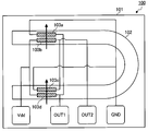
- Fig. 1 shows an example of a current draw type current sensor.
- the current sensor 100 includes a U-shaped conductor 102 in plan view provided on a substrate 101, GMR elements 103a and 103b provided at one end of the conductor 102, and a GMR provided at the other end. Elements 103c and 103d are provided.
- the magnetization directions of the ferromagnetic fixed layers are aligned in the same direction (see the arrow in FIG. 1), and form a magnetic field detection bridge circuit.
- an induced magnetic field applied from opposite directions to each other at one end and the other end of the U-shaped conductor 102 is detected via four GMR elements 103a to 103d.
- the output signals output from the pair of GMR elements 103 a and 103 b at one end of the conductor 102 In order to measure the current to be measured via the magnetic field detection bridge circuit, the output signals output from the pair of GMR elements 103 a and 103 b at one end of the conductor 102, The output signals output from the other pair of GMR elements 103c and 103d at the other end need to have different signal strengths. For this reason, in the current pull-in type current sensor 100, the conductor 102 is U-shaped, and a current to be measured is passed from one end of the conductor 102 to the other end. The direction in which the current to be measured flows is opposite to the direction in which the current to be measured flows at the other end.
- the direction in which the induced magnetic field is applied to the pair of GMR elements 103a and 103b and the direction in which the induced magnetic field is applied to the other pair of GMR elements 103c and 103d are opposite to each other, and thus the pair of GMR elements 103a and 103b.
- Output signals output from the other pair of output signals output from the other pair of GMR elements 103c and 103d have different signal strengths, and the current to be measured can be measured by the magnetic field detection bridge circuit.
- the output signals output from the pair of GMR elements 103a and 103b and the output signals output from the other pair of GMR elements 103c and 103d are different from each other.
- the current to be measured flows through the conductor 102 curved in a U-shape, interference is generated in the induced magnetic field, the measurement accuracy is lowered, and the resistance of the conductor 102 is increased, resulting in a loss of the current to be measured. Since heat generation occurs, there is a problem that the measurement range of the current to be measured is limited.
- the present inventors paid attention to the magnetic field strength of the induced magnetic field from the current to be measured applied to the magnetoresistive effect element and the application direction of the induced magnetic field.
- a conductor extending in one direction is used if an output signal with different signal strength can be obtained from a pair of magnetoresistive elements and another pair of magnetoresistive elements. Even in such a case, the current to be measured can be measured by the magnetic field detection bridge circuit.
- the present inventors paid attention to a self-pinned magnetoresistive effect element that can fix the magnetization direction of the ferromagnetic pinned layer without using an antiferromagnetic layer.
- the self-pinned structure has a laminated structure including a ferromagnetic pinned layer 32, a nonmagnetic intermediate layer 36, and a free magnetic layer 37 as shown in FIG. A structure having no antiferromagnetic layer under the layer 32 is referred to.
- the ferromagnetic pinned layer 32 includes a first ferromagnetic film 33, an antiparallel coupling film 34, and a second ferromagnetic film 35, and the second ferromagnetic film 35 faces the nonmagnetic intermediate layer 36. is doing.
- the magnetization direction X of the ferromagnetic pinned layer 32 of the plurality of magnetoresistive effect elements provided on the substrate can be fixed in an arbitrary direction. It becomes.
- the present inventors also have a pair of magnetoresistive effect elements and another pair of magnetoresistive elements.
- the pair of magnetoresistance effect elements and the other pair of magnetoresistance effect elements are different from each other. It has been found that an output signal of signal strength can be obtained. This makes it possible to measure the current to be measured by the magnetic field detection bridge circuit using the output signals from the pair of magnetoresistive elements and the output signals from the other pair of magnetoresistive elements.
- Such a configuration can be realized by using at least two pairs of self-pinning type magnetoresistive effect elements in a current drawing type current sensor that draws a current to be measured into a conductor on a substrate.
- the present inventors can reduce the size of the substrate and reduce the size of the current sensor by using a conductor extending in one direction in the current-drawing type current sensor.
- the inventors have found that interference can be reduced and measurement accuracy can be improved, and that induced electromotive force against an external magnetic field can be suppressed, and the present invention has been completed.
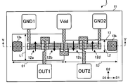
- FIG. 2 is a schematic plan view of the current sensor 1 according to the first embodiment of the present invention.
- the current sensor 1 according to the present embodiment includes a substrate 11 and four magnetoresistive elements 12 a that are arranged on the substrate 11 and output an output signal by an induced magnetic field from a current to be measured.
- the conductor 13 is provided so as to extend in one direction along the magnetoresistive effect elements 12a to 12d arranged in parallel on the substrate 11, and electrode pads 13a for drawing a current to be measured from the outside to both ends. 13b is provided.
- a current to be measured that is drawn from the outside through the electrode pads 13a and 13b and flows through the conductor 13 in one direction includes four magnetoresistive effect elements 12a to 12d. It measures with the magnetic field detection bridge circuit which becomes.
- the conductor 13 has, in the extending direction D1, a first section S1 and a second section S2 having different cross-sectional areas in the vertical section along the height direction D3 orthogonal to the extending direction D1.
- the conductor 13 electrode pad 13a side is defined as a first section S1 having a relatively large cross-sectional area
- electrode pad 13b side is defined as a second section S2 having a relatively small cross-sectional area.
- the magnetoresistance effect elements 12a to 12d are arranged so as to overlap the conductor 13 along the extending direction D1 of the conductor 13.
- the magnetoresistive effect elements 12a to 12d are disposed in the same plane (see FIG. 5), and the pair of magnetoresistive effect elements 12a and 12b are arranged along the first section S1 of the conductor 13.
- the other pair of magnetoresistive elements 12c and 12d are disposed along the second section S2 of the conductor 13.
- the magnetoresistive effect elements 12a to 12d output signals from the pair of magnetoresistive effect elements 12a and 12b and the other pair of magnetoresistive effect elements 12c and 12d by the induced magnetic field from the current to be measured. If the output signals are different in signal strength from each other, it is not always necessary to arrange them in the same plane.
- the sensitivity axes (Pin direction) of the pair of magnetoresistive effects 12a and 12b and the sensitivity axes (Pin direction) of the other pair of magnetoresistive effect elements 12c and 12d are antiparallel to each other ( 180 ° different directions).
- the pair of magnetoresistive elements 12a and 12b are arranged so that the sensitivity axes (Pin directions) of the magnetoresistive elements 12a and 12b are antiparallel to each other (direction different by 180 °).
- the magnetoresistive effect elements 12c and 12d are arranged so that the sensitivity axes (Pin directions) of the magnetoresistive effect elements 12c and 12d are antiparallel to each other (a direction different by 180 °).
- arrows attached to the magnetoresistive effect elements 12a to 12d indicate the magnetization directions of the second ferromagnetic films 35 (not shown in FIG. 1, refer to FIG. 6) of the magnetoresistive effect elements 12a to 12d.
- a hard bias layer 14 (FIG. 1) for applying a bias magnetic field to the free magnetic layer 37 (not shown in FIG. 1, see FIG. 6) of the magnetoresistive effect elements 12a to 12d. (Not shown, see FIG. 5). Note that the hard bias layer 14 is not necessarily provided.
- the magnetoresistive elements 12a to 12d are GMR elements having a shape (a meander shape) formed by folding a plurality of strip-like long patterns (stripes) arranged so that their longitudinal directions are parallel to each other. preferable.
- a power supply potential (Vdd) is applied to one terminal of the magnetoresistive effect element 12b and one terminal of the magnetoresistive effect element 12c, respectively, and one terminal of the magnetoresistive effect element 12a and the magnetoresistive effect element 12d.
- One terminal is supplied with a ground potential (GND1, GND2).
- GND1, GND2 ground potential
- the other terminal of the magnetoresistive effect element 12a and the other terminal of the magnetoresistive effect element 12b are connected to form a first output (Out1), and the other terminal of the magnetoresistive effect element 12c, and The other terminals of the magnetoresistive effect element 12c are connected to form a second output (Out2).
- the magnetoresistive effect elements 12a to 12d have a characteristic that the resistance value changes when an induced magnetic field from the current to be measured is applied, the first output (in accordance with the induced magnetic field from the current to be measured ( Out1) and the second output (Out2) change.
- the potential difference between the first output (Out1) and the second output (Out2) is proportional to the induced magnetic field, and the potential difference (voltage) becomes the output of the current sensor 1.
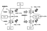
- FIG. 3 is a schematic diagram showing a magnetic detection bridge circuit in the current sensor according to the present embodiment.
- the magnetization directions (second second) of the ferromagnetic pinned layers 32 of the two magnetoresistive elements 12a and 12b that output the midpoint potential (Out1) are output.
- the magnetization direction (Pin2) of the ferromagnetic film is 180 ° different from each other (anti-parallel), and the magnetization direction (the first direction) of the ferromagnetic pinned layer 32 of the two magnetoresistive effect elements 12c and 12d that output the midpoint potential (Out2).
- the magnetization directions of the two ferromagnetic films (Pin2) are 180 ° different from each other (antiparallel).
- the resistance change rates of the four magnetoresistive elements 12a to 12d are the same.
- the magnetoresistive effect elements 12a to 12d preferably exhibit the same rate of change in resistance at the same magnetic field strength when the angle of the applied magnetic field to the ferromagnetic pinned layer 32 is the same.
- 12d a pair of magnetoresistive elements 12a and 12b constitutes a first half bridge circuit
- another pair of magnetoresistive elements 12c and 12d constitutes a second half bridge circuit.
- the conductor 13 has a cross-sectional area in the first section S1 in the vicinity of the magnetoresistive effect elements 12a and 12b in the second section in the vicinity of the magnetoresistive effect elements 12c and 12d. Since it is larger than the cross-sectional area of the conductor 13 in S2, an induced magnetic field A having a relatively small magnetic field strength is applied to the magnetoresistive elements 12a and 12b.
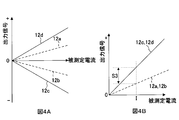
- FIG. 4 is a conceptual diagram showing the correlation between the magnitude of the current to be measured and the output signals from the magnetoresistive elements 12a to 12d.
- the horizontal axis represents the magnitude of the induced magnetic field
- the vertical axis represents the magnitude of the output signal.
- the output signals output from the pair of magnetoresistive effect elements 12a and 12b arranged along the first section S1 of the conductor 13 are in opposite phases and have the same strength (see FIG. 4A). (See dashed line 4A).
- the output signals output from the other pair of magnetoresistive elements 12c and 12d disposed along the second section S2 of the conductor 13 are in reverse phase with each other, have the same strength, and have a pair of magnetic fields. It becomes relatively large with respect to the output signals output from the resistance effect elements 12a and 12b (see the solid line in FIG. 4A). For this reason, as shown in FIG.
- the magnetization directions of the ferromagnetic pinned layers 32 of the magnetoresistive effect elements 12a and 12d are made the same, and the ferromagnetic pinned layers of the magnetoresistive effect elements 12a and 12d are aligned.
- the magnetization direction of 32 the magnetization direction of the ferromagnetic fixed layer 32 of the magnetoresistive effect elements 12b and 12c is aligned in an antiparallel direction (a direction different by 180 °).
- the output signals output from the pair of magnetoresistive elements 12a and 12b by the induced magnetic field A and the output signals output from the other pair of magnetoresistive elements 12c and 12d are reversed in phase
- the output signals output from the pair of magnetoresistive elements 12a and 12b due to the disturbance noise B are equal to the output signals output from the other pair of magnetoresistive elements 12c and 12d. Therefore, by obtaining a differential output between the output signals from the pair of magnetoresistive elements 12a and 12b and the output signals from the other pair of magnetoresistive elements 12c and 12d, Since addition and disturbance noise can be canceled, measurement accuracy and detection sensitivity can be improved. Therefore, a current sensor with high detection sensitivity and measurement accuracy can be realized.
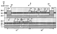
- FIG. 5 is a cross-sectional view taken along line VV of the current sensor 1 shown in FIG.
- a magnetic field detection bridge circuit magnetoresistance effect elements 12a to 12d
- a conductor 13 are stacked on the same substrate 11.
- a silicon oxide film 21 that is an insulating layer is formed on a substrate 11.
- An aluminum oxide film 22 is formed on the silicon oxide film 21.
- the aluminum oxide film 22 can be formed by a method such as sputtering. Further, a silicon substrate or the like is used as the substrate 11.
- magnetoresistive effect elements 12a to 12d are arranged to form a magnetic field detection bridge circuit.
- the magnetoresistive elements 12a to 12d TMR elements (tunnel type magnetoresistive elements), GMR elements (giant magnetoresistive elements), and the like can be used.
- Hard bias layers 14 for applying a bias magnetic field to the free magnetic layer 37 of the magnetoresistive effect elements 12a to 12d are provided at both ends of the magnetoresistive effect elements 12a to 12d.
- a conductor 13 (current line to be measured) is laminated via an insulating layer 23.
- the conductor 13 can be formed by photolithography and plating after forming a base material by sputtering or the like.
- Electrodes 13 a and 13 b are formed at both ends of the conductor 13.
- the electrode pads 13a and 13b can be formed by photolithography and plating after forming an electrode material.
- a polyimide layer formed by applying and curing a polyimide material can be used.
- a high magnetic permeability material such as an amorphous magnetic material, a permalloy magnetic material, or an iron microcrystalline material can be used.
- a silicon oxide film 26 is laminated on the magnetic shield 25.
- the silicon oxide film 26 can be formed by a method such as sputtering.
- a contact hole 27 is formed in a predetermined region of the insulating layer 24 and the silicon oxide film 26 (region where the electrode pads 13a and 13b are formed), and the electrode pads 13a and 13b are formed in the contact hole 27.
- photolithography, etching, or the like is used for forming the contact hole 27.
- the magnetic detection bridge circuit is configured by the four magnetoresistive effect elements 12a to 12d having the same film configuration, the zero magnetic field resistance value (R 0 ) between the elements and the resistance temperature coefficient ( TCR 0 ) can be eliminated. For this reason, variation in the midpoint potential can be reduced regardless of the environmental temperature, and current measurement can be performed with high accuracy.
- the current sensor 1 having the above configuration can be reduced in size because the conductor 13, the magnetic shield 25, and the magnetic field detection bridge circuit (the magnetoresistive effect elements 12a to 12d) are stacked on the same substrate. . Furthermore, since the current sensor 1 has a configuration without a magnetic core, it can be reduced in size and cost.
- FIG. 6 is a schematic cross-sectional view showing a laminated structure of magnetoresistive elements 12a to 12d of the current sensor 1 according to the present embodiment.
- the magnetoresistive effect elements 12a to 12d are stacked on the aluminum oxide film 22.
- the magnetoresistive effect elements 12a to 12d include a seed layer 31, a ferromagnetic pinned layer 32 (a first ferromagnetic film 33, an antiparallel coupling film 34, and a second ferromagnetic film 35), a nonmagnetic intermediate layer 36, a free layer
- the magnetic layer 37 and the protective layer 38 are laminated in this order.
- the first ferromagnetic film 33 and the second ferromagnetic film 35 are antiferromagnetically coupled via the antiparallel coupling film 34, so-called self-pinning type.
- a ferromagnetic pinned layer 32 (SFP: Synthetic Ferri Pinned layer) is formed.
- SFP Synthetic Ferri Pinned layer
- Annealing in a magnetic field for fixing the magnetization direction of a certain ferromagnetic pinned layer 32 becomes unnecessary, and the induced magnetic anisotropy in the stripe longitudinal direction D1 imparted during the formation of the free magnetic layer 37 can be maintained. Thereby, it becomes possible to reduce hysteresis with respect to the detection target direction.
- the thickness of the antiparallel coupling film 34 is set to 0.3 nm to 0.45 nm, or 0.75 nm to 0.95 nm, so that the first ferromagnetic film 33 and the second ferromagnetic film 33 Strong antiferromagnetic coupling with the ferromagnetic film 35 can be brought about.
- the magnetization amount (Ms ⁇ t) of the first ferromagnetic film 33 and the magnetization amount (Ms ⁇ t) of the second ferromagnetic film 35 are substantially the same. That is, the difference in magnetization between the first ferromagnetic film 33 and the second ferromagnetic film 35 is substantially zero. For this reason, the effective anisotropic magnetic field of the ferromagnetic fixed layer 32 is large. Therefore, sufficient magnetization stability of the ferromagnetic pinned layer 32 can be ensured without using an antiferromagnetic material.
- the magnetoresistive effect elements 12a to 12d used in the current sensor 1 have a film configuration that does not have an antiferromagnetic layer.
- Formula (1) eff Hk 2 (K ⁇ t 1 + K ⁇ t 2 ) / (Ms ⁇ t 1 ⁇ Ms ⁇ t 2 )
- the Curie temperature (Tc) of the first ferromagnetic film 33 and the Curie temperature (Tc) of the second ferromagnetic film 35 are the same. Thereby, even in a high temperature environment, the difference in magnetization (Ms ⁇ t) between the first ferromagnetic film 33 and the second ferromagnetic film 35 becomes zero, and high magnetization stability can be maintained.
- the first ferromagnetic film 33 is preferably made of a CoFe alloy containing 40 atomic% to 80 atomic% of Fe. This is because a CoFe alloy having this composition range has a large coercive force and can stably maintain magnetization with respect to an external magnetic field.
- the second ferromagnetic film 35 is preferably composed of a CoFe alloy containing 0 atomic% to 40 atomic% of Fe. This is because the CoFe alloy having this composition range has a small coercive force and is easily magnetized in an antiparallel direction (a direction different by 180 °) with respect to the direction in which the first ferromagnetic film 33 is preferentially magnetized. is there.
- a magnetic field is applied to the first ferromagnetic film 33 and the second ferromagnetic film 35 in the stripe width direction of the meander shape during the film formation, and the first ferromagnetic film 33 and the second strong film after the film formation are applied. It is preferable that induced magnetic anisotropy is imparted to the magnetic film 35. As a result, the first ferromagnetic film 33 and the second ferromagnetic film 35 are magnetized antiparallel to the stripe width direction.
- the magnetization directions (directions in which the magnetization is fixed) of the first ferromagnetic film 33 and the second ferromagnetic film 35 are determined by the magnetic field application direction when the first ferromagnetic film 33 is formed. It is possible to form a plurality of magnetoresistive elements having ferromagnetic pinned layers having different magnetization directions on the same substrate by changing the direction of magnetic field application during the formation of the ferromagnetic film 33.
- the seed layer 31 is made of NiFeCr or Cr.
- the protective layer 38 is made of T or the like.
- the aluminum oxide film 22 and the seed layer 31 are made of a nonmagnetic material such as at least one element of Ta, Hf, Nb, Zr, Ti, Mo, and W, for example.
- An underlayer may be provided.
- the antiparallel coupling film 34 of the ferromagnetic pinned layer 32 is made of Ru or the like.
- the free magnetic layer (free layer) 37 is made of a magnetic material such as a CoFe alloy, a NiFe alloy, or a CoFeNi alloy.
- the nonmagnetic intermediate layer 36 is made of Cu or the like. Further, it is preferable that a magnetic field is applied to the free magnetic layer 37 in the stripe longitudinal direction D1 during film formation, and induced magnetic anisotropy is imparted to the free magnetic layer 37 after film formation.
- the resistance is linearly changed with respect to the external magnetic field (magnetic field from the current to be measured) in the stripe width direction orthogonal to the stripe longitudinal direction D1, and the hysteresis can be reduced. it can.
- a spin valve configuration is adopted by the ferromagnetic pinned layer 30, the nonmagnetic intermediate layer 36 and the free magnetic layer 37.
- the film configuration of the magnetoresistive effect elements 12a to 12d used in the current sensor 1 for example, NiFeCr (seed layer 31: 5 nm) / Fe 70 Co 30 (first ferromagnetic film 33: 1.65 nm) / Ru (anti-parallel coupling film 34: 0.4 nm) / Co 90 Fe 10 (second ferromagnetic film 35: 2 nm) / Cu (nonmagnetic intermediate layer 36: 2.2 nm) / Co 90 Fe 10 (free magnetic layer 37: 1 nm) / Ni 81 Fe 19 (free magnetic layer 37: 7 nm) / Ta (protective layer 38: 5 nm).
- the first ferromagnetic film 33 and the second ferromagnetic film 35 are anti-bonded on the aluminum oxide film 22 via the anti-parallel coupling film 34.
- a magnetoresistive effect element 12a to 12 having a self-pinned ferromagnetic fixed layer 32, a nonmagnetic intermediate layer 36, and a free magnetic layer 37 that are ferromagnetically coupled and whose magnetization direction is fixed in a specific direction.
- first forming step the first laminated film in a region other than the region where the first laminated film is left is removed from the aluminum oxide film 22 (removing step), and the first laminated film is removed.
- Self-pinning type ferromagnetic pinning in which the first ferromagnetic film 33 and the second ferromagnetic film 35 are antiferromagnetically coupled to the removed aluminum oxide film 22 via the antiparallel coupling film 34.
- the magnetoresistive effect elements 12 a and 12 b having different magnetization directions of the ferromagnetic pinned layer 32 can be provided close to each other on the same substrate 11. Further, by repeatedly performing the removing step and the second forming step, it is possible to provide a plurality of magnetoresistive elements 12a to 12d having different magnetization directions of the ferromagnetic pinned layer 32 on the same substrate 11.
- FIGS. 7A to 7C and FIGS. 8A to 8C are explanatory diagrams of a method of manufacturing the magnetoresistive effect elements 12a to 12d in the current sensor 1 according to the present embodiment.
- the magnetoresistive effect elements 12b and 12c are formed after the magnetoresistive effect elements 12a and 12d are formed.
- a seed layer 31 on the aluminum oxide film 22, a seed layer 31, a first ferromagnetic film 33, an antiparallel coupling film 34, a second ferromagnetic film 35, a nonmagnetic intermediate layer 36, a free magnetic layer.
- a layer 37 and a protective layer 38 are sequentially formed.
- a magnetic field is applied in the meander-shaped stripe width direction. 7A to 7C, with respect to the first ferromagnetic film 33 (Pin1), the applied magnetic field direction is the direction from the back side to the near side of the paper, and the second ferromagnetic film 35 (Pin2) is applied.
- the direction of the magnetic field is the direction from the front side to the back side of the page.
- the same direction as the first ferromagnetic film 33 or no magnetic field may be used.
- a resist layer 40 is formed on the protective layer 38, and the resist layer 40 is left on the regions of the magnetoresistive effect elements 12a and 12d by photolithography and etching.
- the exposed laminated film is removed by ion milling or the like to expose the aluminum oxide film 22 in the region where the magnetoresistive effect elements 12b and 12c are provided.
- the seed layer 31 After removing the resist layer 40, the seed layer 31, the first ferromagnetic film 33, the antiparallel coupling film 34, and the second ferromagnetic material are formed on the exposed aluminum oxide film 22.
- a magnetic field is applied in the meander-shaped stripe width direction.
- the direction of the applied magnetic field is the direction from the back side to the front side of the page, and the magnetoresistive effect 12b
- the direction of the applied magnetic field is the direction from the front side of the page toward the back side of the page.
- the direction of the applied magnetic field is the direction from the front side to the back side of the paper surface, and the second ferromagnetic film 35 that becomes the magnetoresistive effects 12b and 12c.
- the applied magnetic field direction is the direction from the back side to the front side of the drawing.
- a magnetic field is applied in the longitudinal direction of the meander stripe.
- a resist layer 40 is formed on the protective layer 38, and the resist layer 40 is left on the formation regions of the magnetoresistive effect elements 12a, 12b, 12c, and 12d by photolithography and etching.
- the exposed laminated film is removed by ion milling or the like, and magnetoresistive effect elements 12a, 12b, 12c, and 12d are formed in an arrangement as shown in FIG.
- the magnetization direction of the ferromagnetic fixed layer 32 without providing an antiferromagnetic layer. can be fixed in any direction, so that the magnetization direction of the ferromagnetic pinned layer 32 of each of the magnetoresistive effect elements 12a to 12d can be set to an arbitrary direction even when four magnetoresistive effect elements are arranged in parallel on the substrate. Can be fixed.
- a current-drawing type current sensor using a conductor extending in one direction can be realized, so that the current to be measured flows through the conductor 13 as compared with the case where a conductor having a curved shape is used.
- the resistance due to the conductor 13 can be reduced, and the loss of the current to be measured and the heat generation due to the flow of the current to be measured can be suppressed. Furthermore, since the direction of the induced magnetic field from the current to be measured can be aligned, it is possible to suppress the interference of the induced magnetic field and the generation of induced electromotive force against the disturbance magnetic field, and a current sensor with a wide measurement range and high measurement accuracy can be obtained. realizable.
- the pair of magnetoresistive elements 12a and 12b are disposed along the first section S1 having a relatively large cross-sectional area of the conductor 13, and the other pair of magnetoresistive elements. Since 12c and 12d are disposed along the second section S2 having a relatively small cross-sectional area, an induced magnetic field applied to the pair of magnetoresistive elements 12a and 12b and another pair of magnetoresistances The effect elements 12c and 12d and the induced magnetic field applied have different magnetic field strengths. Accordingly, the output signals output from the pair of magnetoresistive effect elements 12a and 12b and the output signals output from the other pair of magnetoresistive effect elements 12c and 12d have different signal strengths.
- the measured current can be measured by the magnetic field detection bridge circuit without using.
- the magnetization direction of the ferromagnetic pinned layer 32 of the pair of magnetoresistive effect elements 12a and 12b and the magnetization direction of the ferromagnetic pinned layer 32 of the other pair of magnetoresistive effect elements 12c and 12d are fixed in the same direction. Therefore, the output signals output from the pair of magnetoresistance effect elements 12a and 12b and the output signals output from the other pair of magnetoresistance effect elements 12c and 12d are in phase due to disturbance noise. Furthermore, due to the current to be measured, the induced magnetic field applied to the pair of magnetoresistive effect elements 12a and 12b and the induced magnetic field applied to the other pair of magnetoresistive effect elements 12c and 12d have different magnetic field strengths.
- the differential output is appear.
- an output signal derived from an induced magnetic field from the current to be measured is obtained by a differential output between the output signals of the pair of magnetoresistive effect elements 12a and 12b and the output signals of the other pair of magnetoresistive effect elements 12c and 12d.
- disturbance noise components are canceled out, so that a current sensor with high detection sensitivity and high measurement accuracy can be realized.
- the magnetic field detection bridge circuit can be configured without using a fixed resistance element, so that offset can be reduced and a conductor extending in one direction can be used. Since the current to be measured can be measured, the area of the substrate can be reduced, and the current sensor can be downsized and the manufacturing cost can be reduced. In addition, since it is possible to configure the magnetoresistive element without using an antiferromagnetic material, it is possible to ensure the stability of the operation of the current sensor 1 even in a high temperature environment and not to use an antiferromagnetic material. Therefore, it is possible to reduce the manufacturing cost because the material cost and the annealing process in the magnetic field are not required.
- the magnetic detection bridge circuit is composed of four magnetoresistive effect elements having the same film configuration, the zero magnetic field resistance value (R 0 ) and the resistance temperature coefficient between the elements.
- the deviation of (TCR 0 ) can be eliminated. For this reason, the variation in the midpoint potential can be reduced regardless of the environmental temperature, and the measurement accuracy of the current to be measured can be improved.
- the pair of magnetoresistive elements 12a and 12b are disposed with the region on the electrode pad 13a side of the conductor 13 as the first section S1, and the region on the electrode pad 13b side of the conductor 13 is defined.
- the configuration in which the other pair of magnetoresistive effect elements 12c and 12d is provided as the second section S2 has been described.
- the arrangement of the magnetoresistive effect elements 12a to 12d is a pair of the magnetoresistive effect elements 12a and 12b and the other pair. As long as the arrangement is such that output signals having different signal strengths are output from the magnetoresistive effect elements 12c and 12d, the magnetoresistive effect elements 12c and 12d can be appropriately changed.
- both ends of the conductor 13 in the extending direction D1 are respectively set as the first section S1, and the pair of magnetoresistive effect elements 12a and 12b are respectively disposed, and the section between the first sections S1 is set as the second section S2.
- Another pair of magnetoresistive elements 12c and 12d may be provided.
- the first section S1 and the second section S2 are provided alternately from the electrode pad 13a side to the electrode pad 13b side of the conductor 13, thereby providing a pair of magnetoresistive elements. You may arrange
- the width dimension L1 of 1st area S1 and the width dimension L2 of 2nd area S2 are made into different magnitude
- the configuration of the conductor 13 having S2 has been described, a configuration in which the cross-sectional areas of the first section S1 and the second section S2 are made different from each other is a pair of magnetoresistance effect elements 12a and 12b and another pair of magnetoresistance effects. If output signals having different signal intensities are output from the elements 12c and 12d, they can be appropriately changed.
- the width dimensions L1 and L2 of the conductor 13 are the same, and the dimensions (thicknesses) in the height direction D3 perpendicular to the extending direction D1 and the width direction D2 of the conductor 13 are different from each other.
- the conductor 13 having the first section S1 and the second section S2 may be used.
- FIG. 9 is a schematic plan view of the current sensor 2 according to the present embodiment
- FIG. 10 is a schematic cross-sectional view taken along the line XX in FIG.
- the conductor 51 is provided so as to extend in one direction, and has a uniform width dimension L1.
- the magnetoresistance effect elements 12a to 12d are arranged in parallel along the extending direction D1 of the conductor 51.
- the pair of magnetoresistive elements 12a and 12b are disposed in the first plane (see F1) in the first section S1, and the other pair of magnetoresistive elements 12c and 12d are second. In the section S2, it is disposed in the second plane (see F2).
- the distance L3 between the pair of magnetoresistance effect elements 12a and 12b and the conductor 13 in the height direction D3 of the conductor 13, and the other pair of magnetoresistance effect elements 12c and 12d Since the distance L4 between the conductor 13 and the conductor 13 is different from each other, the induced magnetic field applied to the pair of magnetoresistive elements 12a and 12b and the induced magnetic field applied to the other pair of magnetoresistive elements 12c and 12d And have different magnetic field strengths. As a result, the output signals output from the pair of magnetoresistive elements 12a and 12b and the output signals output from the other pair of magnetoresistive elements 12c and 12d have different signal intensities.
- the current to be measured can be measured by the circuit.
- a silicon oxide film 21 is provided on the substrate 11, and magnetoresistive effect elements 12a and 12b are disposed on the silicon oxide film 21 via an aluminum oxide film 22.
- Hard bias layers 14 for applying a bias magnetic field to the free magnetic layers 37 of the magnetoresistive effect elements 12a and 12b are provided at both ends of the magnetoresistive effect elements 12a and 12b.
- An insulating layer 23, an aluminum oxide film 52, an insulating layer 53, a conductor 51, and the like are stacked on the magnetoresistive effect elements 12a and 12b.
- a silicon oxide film 21, an aluminum oxide film 22, and an insulating layer 23 are stacked in this order on the substrate 11, and the magnetoresistive effect element 12 c is formed on the insulating layer 23 via an aluminum oxide film 52. , 12d are disposed.
- Hard bias layers 14 for applying a bias magnetic field to the free magnetic layers 37 of the magnetoresistive effect elements 12c and 12d are provided at both ends of the magnetoresistive effect elements 12c and 12d.
- An insulating layer 53, a conductor 51, and the like are stacked on the magnetoresistive effect elements 12a and 12b. Since the other laminated structure is the same as that of the current sensor 1 according to the first embodiment, the description thereof is omitted.
- the current sensor 2 has a different stacked structure in the region on the electrode pad 13a side of the conductor 51 and the region on the electrode pad 13b side, and the pair of magnetoresistive effect elements 12a and 12b and the conductor 13 are provided. Is larger than the distance L4 between the other pair of magnetoresistive elements 12c and 12b and the conductor 13.
- the magnetic field strength of the induced magnetic field applied to the pair of magnetoresistive effect elements 12a and 12b is relative to the magnetic field strength of the induced magnetic field applied to the other pair of magnetoresistive effect elements 12c and 12d.
- the output signals output from the pair of magnetoresistive elements 12a and 12b and the output signals output from the other pair of magnetoresistive elements 12c and 12d have different signal strengths. It becomes possible to measure the current to be measured.
- FIG. 11 is a schematic cross-sectional view of the current sensor 3 according to the present embodiment.
- the conductor 61 includes first and second conductive paths 61a and 61b extending in the same direction, and the first conductive path 61a and the second conductive path 61b. And a third conductive path 61c to be connected.
- the first and second conductive paths 61a and 61b are provided so as to extend parallel to the surface of the substrate 11, and the relative positions in the height direction D3 orthogonal to the extending direction D1 of the conductor 61 are They are provided differently.
- the first conductive path 61a is the first section S1
- the second conductive path 61b is the second section S2.
- the conductor 61 is provided such that the distance between the surface of the substrate 11 and the first conductive path 61a is smaller than the distance between the surface of the substrate 11 and the second conductive path 61b. It is done.
- An electrode pad 13a is provided on one end side of the first conductive path 61a, and an electrode pad 13b is provided on the other end side of the second conductive path 61b.
- the other end of the first conductive path 61a and one end of the second conductive path 61b are connected by a third conductive path 61c.
- the magnetoresistive elements 12a to 12d are juxtaposed along the extending direction of the conductor 61, and are arranged in the same plane (see F3).
- a pair of magnetoresistive elements 12a and 12b are disposed along the first conductive path 61a, and the other pair of magnetoresistive elements 12c and 12d are disposed along the second conductive path 61b. .
- the distance L5 between the pair of magnetoresistive elements 12a and 12b and the first conductor 61a is other than It arrange
- the magnetoresistive effect elements 12a to 12d are output from the pair of magnetoresistive effect elements 12a and 12b and the other pair of magnetoresistive effect elements 12c and 12d by the induced magnetic field from the current to be measured.
- the configuration is not limited to the configuration in which the output signals are arranged in the same plane.
- the distance L5 between the pair of magnetoresistive elements 12a and 12b and the first conductive path 61a is equal to the other pair of magnetoresistive elements 12c
- the distance L6 is smaller than the distance L6 between 12d and the second conductive path 61b
- the magnetic field strength of the induced magnetic field applied to the pair of magnetoresistive elements 12a and 12b is different from that of the other pair of magnetoresistive elements 12c.
- 12d becomes relatively large with respect to the magnetic field strength of the induction magnetic field applied to 12d.
- the output signals output from the pair of magnetoresistive elements 12a and 12b and the output signals output from the other pair of magnetoresistive elements 12c and 12d have different signal strengths. It becomes possible to measure the current to be measured.
- FIG. 12 is a schematic cross-sectional view of the current sensor 4 according to the present embodiment.
- the pair of magnetoresistive elements 12a and 12b and the other pair of magnetoresistive elements 12c and 12d have an application direction of an induced magnetic field from the current I to be measured. It arrange
- the pair of magnetoresistive elements 12a and 12b are arranged on the lower surface side in the first section S1 on the electrode pad 13a side of the conductor 13 with respect to the extending direction of the conductor 13 in a sectional view.
- the other pair of magnetoresistive elements 12c and 12d are disposed on the upper surface side in the second section S2 on the electrode pad 13b side of the conductor 13 with respect to the extending direction of the conductor 13 in a sectional view.
- the induced magnetic field when the current I to be measured flows through the conductor 13 from the electrode pad 13a side to the electrode pad 13b side is from the front side of the sheet with respect to the pair of magnetoresistive effect elements 12a and 12b. It is applied toward the back side of the paper, and applied to the other pair of magnetoresistive elements 12c and 12d from the back side of the paper toward the front of the paper.
- the output signals output from the pair of magnetoresistive elements 12a and 12b and the output signals output from the other pair of magnetoresistive elements 12b are out of phase, so that the current to be measured can be measured. It becomes.
- a silicon oxide film 21 is provided on the substrate 11, and magnetoresistive effect elements 12a and 12b are disposed on the silicon oxide film 21 via an aluminum oxide film 22.
- Hard bias layers 14 for applying a bias magnetic field to the free magnetic layers 37 of the magnetoresistive effect elements 12a and 12b are provided at both ends of the magnetoresistive effect elements 12a and 12b.
- the insulating layer 24, the conductor 13, the insulating layer 24, the aluminum oxide film 52, and the silicon oxide film 26 are laminated in this order.
- a silicon oxide film 21, an aluminum oxide film 22, an insulating layer 23, a conductor 13, and an insulating layer 24 are stacked in this order on the substrate 11, and an aluminum oxide film is formed on the insulating layer 24.
- the magnetoresistive effect elements 12 c and 12 d are disposed via 52.
- Hard bias layers 14 for applying a bias magnetic field to the free magnetic layers 37 of the magnetoresistive effect elements 12c and 12d are provided at both ends of the magnetoresistive effect elements 12c and 12d.
- a silicon oxide film 26 is laminated on the magnetoresistive effect elements 12c and 12d.
- the other laminated structure is the same as that of the current sensors 1, 2, and 3 according to the first, second, and third embodiments, and thus the description thereof is omitted.
- the pair of magnetoresistive elements 12a and 12b and the other pair of magnetoresistive elements 12c and 12d apply an induced magnetic field from the current to be measured. It arrange
- the direction in which the induction magnetic field is applied to the pair of magnetoresistance effect elements 12a and 12b and the direction in which the induction magnetic field is applied to the other pair of magnetoresistance effect elements 12c and 12d are different from each other.
- the output signals output from the resistance effect elements 12a and 12b and the output signals output from the other pair of magnetoresistance effect elements 12c and 12d have different signal strengths. As a result, the current to be measured can be detected by the magnetic field detection bridge circuit.
- the present invention has the effect of realizing a current sensor that has excellent operational stability at high temperatures and high measurement accuracy, and in particular, various current sensors and current sensors that detect the magnitude of current for driving motors in electric vehicles. It is possible to apply to.
Landscapes
- Physics & Mathematics (AREA)
- General Physics & Mathematics (AREA)
- Chemical & Material Sciences (AREA)
- Engineering & Computer Science (AREA)
- Nanotechnology (AREA)
- Condensed Matter Physics & Semiconductors (AREA)
- Crystallography & Structural Chemistry (AREA)
- Measuring Magnetic Variables (AREA)
- Measuring Instrument Details And Bridges, And Automatic Balancing Devices (AREA)
- Hall/Mr Elements (AREA)
Abstract
L'invention porte sur un capteur de courant, qui présente une excellente stabilité de fonctionnement à haute température, et une précision de mesure élevée. Un capteur de courant (1) de la présente invention est caractérisé en ce qu'il comporte : un corps conducteur (13), qui s'étend dans une direction ; et des éléments à effet magnéto-résistif (12a-12d), qui sont disposés en parallèle dans la direction d'extension du corps conducteur (13), et qui émettent des signaux de sortie au moyen d'un champ magnétique inducteur provenant d'un courant à mesurer, ledit courant circulant dans le corps conducteur (13). Le capteur de courant est également caractérisé en ce que les éléments à effet magnéto-résistif (12a-12d) comprennent une paire d'éléments à effet magnéto-résistif (12a, 12b), qui sont disposés le long d'une première section (S1) du corps conducteur (13), et une autre paire d'éléments à effet magnéto-résistif (12c, 12d), qui sont disposés le long d'une seconde section (S2) du corps conducteur (13), et en ce que la paire d'éléments à effet magnéto-résistif (12a, 12b) et l'autre paire d'éléments à effet magnéto-résistif (12c, 12d) sont disposés de sorte que le champ magnétique inducteur soit appliqué à ceux-ci à des intensités différentes les unes des autres ou à partir de directions différentes les unes des autres.
Priority Applications (1)
| Application Number | Priority Date | Filing Date | Title |
|---|---|---|---|
| JP2013502216A JP5540326B2 (ja) | 2011-03-02 | 2012-01-27 | 電流センサ |
Applications Claiming Priority (2)
| Application Number | Priority Date | Filing Date | Title |
|---|---|---|---|
| JP2011-044711 | 2011-03-02 | ||
| JP2011044711 | 2011-03-02 |
Publications (1)
| Publication Number | Publication Date |
|---|---|
| WO2012117784A1 true WO2012117784A1 (fr) | 2012-09-07 |
Family
ID=46757726
Family Applications (1)
| Application Number | Title | Priority Date | Filing Date |
|---|---|---|---|
| PCT/JP2012/051846 WO2012117784A1 (fr) | 2011-03-02 | 2012-01-27 | Capteur de courant |
Country Status (2)
| Country | Link |
|---|---|
| JP (1) | JP5540326B2 (fr) |
| WO (1) | WO2012117784A1 (fr) |
Cited By (3)
| Publication number | Priority date | Publication date | Assignee | Title |
|---|---|---|---|---|
| JP2018004565A (ja) * | 2016-07-07 | 2018-01-11 | 公益財団法人電磁材料研究所 | 磁気センサモジュール |
| US10545198B2 (en) | 2014-11-18 | 2020-01-28 | Hitachi Metals, Ltd. | Magnetic sensor, manufacturing method thereof, and current detector using the same |
| CN111090063A (zh) * | 2018-10-24 | 2020-05-01 | Tdk株式会社 | 磁传感器 |
Citations (3)
| Publication number | Priority date | Publication date | Assignee | Title |
|---|---|---|---|---|
| JPH01105178A (ja) * | 1987-07-07 | 1989-04-21 | Nippon Denso Co Ltd | 電流検出器 |
| JP2005529338A (ja) * | 2002-06-06 | 2005-09-29 | コーニンクレッカ フィリップス エレクトロニクス エヌ ヴィ | 荷電粒子の流れを測定するためのセンサおよび方法 |
| JP2009180604A (ja) * | 2008-01-30 | 2009-08-13 | Hitachi Metals Ltd | 角度センサ、その製造方法及びそれを用いた角度検知装置 |
-
2012
- 2012-01-27 JP JP2013502216A patent/JP5540326B2/ja active Active
- 2012-01-27 WO PCT/JP2012/051846 patent/WO2012117784A1/fr active Application Filing
Patent Citations (3)
| Publication number | Priority date | Publication date | Assignee | Title |
|---|---|---|---|---|
| JPH01105178A (ja) * | 1987-07-07 | 1989-04-21 | Nippon Denso Co Ltd | 電流検出器 |
| JP2005529338A (ja) * | 2002-06-06 | 2005-09-29 | コーニンクレッカ フィリップス エレクトロニクス エヌ ヴィ | 荷電粒子の流れを測定するためのセンサおよび方法 |
| JP2009180604A (ja) * | 2008-01-30 | 2009-08-13 | Hitachi Metals Ltd | 角度センサ、その製造方法及びそれを用いた角度検知装置 |
Cited By (3)
| Publication number | Priority date | Publication date | Assignee | Title |
|---|---|---|---|---|
| US10545198B2 (en) | 2014-11-18 | 2020-01-28 | Hitachi Metals, Ltd. | Magnetic sensor, manufacturing method thereof, and current detector using the same |
| JP2018004565A (ja) * | 2016-07-07 | 2018-01-11 | 公益財団法人電磁材料研究所 | 磁気センサモジュール |
| CN111090063A (zh) * | 2018-10-24 | 2020-05-01 | Tdk株式会社 | 磁传感器 |
Also Published As
| Publication number | Publication date |
|---|---|
| JP5540326B2 (ja) | 2014-07-02 |
| JPWO2012117784A1 (ja) | 2014-07-07 |
Similar Documents
| Publication | Publication Date | Title |
|---|---|---|
| US8487612B2 (en) | Current sensor | |
| JP5572208B2 (ja) | 磁気センサ及びそれを用いた磁気平衡式電流センサ | |
| JP4930627B2 (ja) | 磁気センサ | |
| WO2010143666A1 (fr) | Capteur de courant à équilibre magnétique | |
| WO2012081377A1 (fr) | Capteur magnétique et son procédé de fabrication | |
| JP5540299B2 (ja) | 電流センサ | |
| WO2012090631A1 (fr) | Capteur de courant proportionnel électromagnétique | |
| US20120306491A1 (en) | Magnetic balance type current sensor | |
| US20130057274A1 (en) | Current sensor | |
| WO2011111537A1 (fr) | Capteur de courant | |
| JP5447616B2 (ja) | 磁気センサの製造方法 | |
| JP7057680B2 (ja) | 磁気センサおよび電流センサ | |
| JP5597305B2 (ja) | 電流センサ | |
| JP5540326B2 (ja) | 電流センサ | |
| JP2011027633A (ja) | 磁気センサおよびその製造方法 | |
| WO2018037634A1 (fr) | Capteur magnétique et capteur de courant | |
| WO2011111457A1 (fr) | Capteur de magnétisme et capteur de courant à balance magnétique associé | |
| JP7122836B2 (ja) | 磁気センサおよび電流センサ | |
| JP2017096691A (ja) | 磁気センサおよびその製造方法、ならびに電流センサ |
Legal Events
| Date | Code | Title | Description |
|---|---|---|---|
| 121 | Ep: the epo has been informed by wipo that ep was designated in this application |
Ref document number: 12753021 Country of ref document: EP Kind code of ref document: A1 |
|
| ENP | Entry into the national phase |
Ref document number: 2013502216 Country of ref document: JP Kind code of ref document: A |
|
| NENP | Non-entry into the national phase |
Ref country code: DE |
|
| 122 | Ep: pct application non-entry in european phase |
Ref document number: 12753021 Country of ref document: EP Kind code of ref document: A1 |