WO2012117757A1 - バイアス制御回路 - Google Patents
バイアス制御回路 Download PDFInfo
- Publication number
- WO2012117757A1 WO2012117757A1 PCT/JP2012/050762 JP2012050762W WO2012117757A1 WO 2012117757 A1 WO2012117757 A1 WO 2012117757A1 JP 2012050762 W JP2012050762 W JP 2012050762W WO 2012117757 A1 WO2012117757 A1 WO 2012117757A1
- Authority
- WO
- WIPO (PCT)
- Prior art keywords
- bias
- amplifier
- current
- circuit
- control circuit
- Prior art date
- Legal status (The legal status is an assumption and is not a legal conclusion. Google has not performed a legal analysis and makes no representation as to the accuracy of the status listed.)
- Ceased
Links
Images




Classifications
-
- H—ELECTRICITY
- H03—ELECTRONIC CIRCUITRY
- H03F—AMPLIFIERS
- H03F1/00—Details of amplifiers with only discharge tubes, only semiconductor devices or only unspecified devices as amplifying elements
- H03F1/26—Modifications of amplifiers to reduce influence of noise generated by amplifying elements
-
- H—ELECTRICITY
- H03—ELECTRONIC CIRCUITRY
- H03F—AMPLIFIERS
- H03F1/00—Details of amplifiers with only discharge tubes, only semiconductor devices or only unspecified devices as amplifying elements
- H03F1/02—Modifications of amplifiers to raise the efficiency, e.g. gliding Class A stages, use of an auxiliary oscillation
- H03F1/0205—Modifications of amplifiers to raise the efficiency, e.g. gliding Class A stages, use of an auxiliary oscillation in transistor amplifiers
- H03F1/0211—Modifications of amplifiers to raise the efficiency, e.g. gliding Class A stages, use of an auxiliary oscillation in transistor amplifiers with control of the supply voltage or current
- H03F1/0216—Continuous control
- H03F1/0222—Continuous control by using a signal derived from the input signal
-
- H—ELECTRICITY
- H03—ELECTRONIC CIRCUITRY
- H03F—AMPLIFIERS
- H03F1/00—Details of amplifiers with only discharge tubes, only semiconductor devices or only unspecified devices as amplifying elements
- H03F1/32—Modifications of amplifiers to reduce non-linear distortion
- H03F1/3205—Modifications of amplifiers to reduce non-linear distortion in field-effect transistor amplifiers
-
- H—ELECTRICITY
- H03—ELECTRONIC CIRCUITRY
- H03F—AMPLIFIERS
- H03F3/00—Amplifiers with only discharge tubes or only semiconductor devices as amplifying elements
- H03F3/189—High-frequency amplifiers, e.g. radio frequency amplifiers
- H03F3/19—High-frequency amplifiers, e.g. radio frequency amplifiers with semiconductor devices only
-
- H—ELECTRICITY
- H03—ELECTRONIC CIRCUITRY
- H03F—AMPLIFIERS
- H03F3/00—Amplifiers with only discharge tubes or only semiconductor devices as amplifying elements
- H03F3/20—Power amplifiers, e.g. Class B amplifiers, Class C amplifiers
- H03F3/24—Power amplifiers, e.g. Class B amplifiers, Class C amplifiers of transmitter output stages
- H03F3/245—Power amplifiers, e.g. Class B amplifiers, Class C amplifiers of transmitter output stages with semiconductor devices only
-
- H—ELECTRICITY
- H03—ELECTRONIC CIRCUITRY
- H03F—AMPLIFIERS
- H03F2200/00—Indexing scheme relating to amplifiers
- H03F2200/102—A non-specified detector of a signal envelope being used in an amplifying circuit
Definitions
- the present invention relates to a bias control circuit that controls the bias of an amplifier.
- OFDM Orthogonal Frequency Division Multiplex
- an envelope tracking method is known.
- Japanese Patent Application Laid-Open No. 2010-206545 detects an envelope of an input signal, and the envelope level exceeds a threshold value.
- International Publication WO02 / 003545 proposes a method of adjusting the bias current of the amplifier by a current mirror circuit following the level fluctuation of the envelope of the input signal.
- JP 2010-206545 A International Publication WO02 / 003545
- an object of the present invention is to propose a bias control circuit that can suppress a decrease in gain with respect to a low-level high-frequency signal while relaxing the distortion characteristics of the amplifier.
- a bias control circuit is a bias control circuit that controls the bias of an amplifier that amplifies a high-frequency signal, and includes a detector that detects an envelope of the high-frequency signal, and a constant amplifier. And a second bias circuit for supplying a bias current, which fluctuates following the level fluctuation of the envelope of the high-frequency signal, to the amplifier. Even when the level of the high-frequency signal is small, since a constant bias current is supplied from the first bias circuit to the amplifier, it is possible to suppress a decrease in gain of the amplifier and to ensure a stable operation. In addition, since the bias current that varies following the level variation of the envelope of the high-frequency signal is supplied from the second bias circuit to the amplifier, the distortion characteristics of the amplifier can be relaxed.
- the first bias circuit preferably supplies a constant bias current to the amplifier irrespective of the envelope level of the high-frequency signal. As a result, even when the level of the high-frequency signal is small, a minimum bias current is supplied to the amplifier, so that a decrease in gain of the amplifier can be suppressed and stable operation can be ensured.
- the second bias circuit preferably supplies the amplifier with a bias current that fluctuates following the fluctuation of the envelope level when the envelope level of the high-frequency signal exceeds a threshold value.
- a bias current that fluctuates following the fluctuation of the envelope level when the envelope level of the high-frequency signal exceeds a threshold value.
- the bias control circuit may further include a current backflow prevention circuit inserted in each current path for supplying a bias current from the first and second bias circuits to the amplifier. Thereby, reverse flow of the bias current between the first bias circuit and the second bias circuit can be prevented.
- the first bias circuit is preferably a current mirror circuit that supplies a bias current obtained by multiplying a reference current having a constant current value by the first mirror ratio regardless of the envelope level of the high-frequency signal
- the second bias circuit supplies a bias current obtained by multiplying a reference current that changes following the envelope level fluctuation by the second mirror ratio when the envelope level of the high-frequency signal exceeds a threshold value.
- a current mirror circuit is preferred. According to the current mirror circuit, it is possible to easily generate a bias current that fluctuates following the fluctuation in the level of the envelope of the high-frequency signal based on the junction area ratio of the transistor, the power supply voltage, the current adjusting resistor, or the like.
- the detector, the first bias circuit, and the second bias circuit are preferably configured to be connected in parallel to the amplifier. Such a circuit configuration is suitable for one-chip integration of the bias control circuit.
- the bias control circuit may further include a third bias circuit that supplies a bias current that fluctuates following the level fluctuation of the envelope of the high-frequency signal to the amplifier. This makes it possible to accurately supply the bias current in consideration of the distortion characteristics of the amplifier.
- the bias control circuit of the present invention it is possible to effectively suppress a decrease in gain with respect to a low-level high-frequency signal while relaxing the distortion characteristics of the amplifier.
- FIG. 3 is a block diagram illustrating a configuration of a bias control circuit according to the first embodiment.
- 3 is a circuit diagram illustrating a configuration of a first bias circuit according to Embodiment 1.
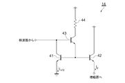
- FIG. 3 is a circuit diagram illustrating a configuration of a second bias circuit according to the first embodiment.
- 6 is a graph showing the operation of the bias control circuit according to the first embodiment.
- FIG. 6 is a block diagram illustrating a configuration of a bias control circuit according to a second embodiment. 6 is a graph illustrating an operation of a bias control circuit according to the second embodiment.
- FIG. 1 is a block diagram showing the configuration of the bias control circuit 10 according to the first embodiment.
- the amplifier 20 is a power amplifier for power-amplifying a high-frequency signal (for example, OFDM modulation signal) input to the input terminal 71 and outputting it to the output terminal 72.
- the amplifier 20 is composed of one or more bipolar transistors and the like.
- a matching circuit 21 for matching the impedance of the input signal source to the input impedance of the amplifier 20 is provided at the front stage of the amplifier 20, and the output stage of the amplifier 20 is matched with the load impedance at the subsequent stage of the amplifier 20.
- a matching circuit 22 is provided.
- the bias control circuit 10 is a circuit for controlling supply of a bias current to the amplifier 20.
- the bias control circuit 10 detects the envelope of the high frequency signal, the first bias circuit 12 that supplies a constant bias current to the amplifier 20, and the level fluctuation (voltage fluctuation) of the envelope of the high frequency signal. And a second bias circuit 14 that supplies the amplifier 20 with a bias current that fluctuates and follows.
- the detector 11, the first bias circuit 12, and the second bias circuit 14 are connected in parallel to the amplifier 20, and are suitable for the one-chip integration of the bias control circuit 10.
- the detector 11 is a known envelope detection circuit, and includes a detection element such as a diode and a smoothing circuit such as a capacitor.
- FIG. 2 is a circuit diagram showing a configuration of the first bias circuit 12.
- the first bias circuit 12 is a current mirror circuit including an input transistor 31, an output transistor 32, and a resistance element 33. As shown in the figure, the gate of the input transistor 31 and the gate of the output transistor 32 are connected, and the source of the input transistor 31 and the source of the output transistor 32 are connected to a common power source. Further, the gate and drain of the input transistor 31 are short-circuited, and a resistance element 33 is connected to the drain.
- the reference current I ref1 flowing through the drain of the input transistor 31 is constant regardless of the level (voltage) of the envelope of the high frequency signal, and the current value is adjusted by the power supply voltage and the resistance element 33.
- the current I 1 flowing through the drain of the output transistor 32 has a current value obtained by multiplying the reference current I ref1 by the first mirror ratio, and is supplied to the amplifier 20 as a constant bias current.
- the first mirror ratio can be adjusted by the junction area ratio of the transistors 31 and 32.
- FIG. 3 is a circuit diagram showing a configuration of the second bias circuit 14.
- the second bias circuit 14 is a current mirror circuit including an input transistor 41, an output transistor 42, a switching transistor 43, and a resistance element 44.
- the collector of the switching transistor 43 is connected to the power supply via the resistance element 44, the base thereof is connected to the output of the detector 11, and the emitter thereof is the base of the input transistor 41 and the base of the output transistor 42.
- the collector of the input transistor 41 is connected to the base of the switching transistor 43, and the collector of the output transistor 42 is connected to the power source.
- the switching transistor 43 is turned on when the level of the envelope of the high-frequency signal input to its base exceeds the first threshold voltage Vth1, and the level of the envelope of the high-frequency signal is less than or equal to the first threshold voltage Vth1.
- the value of the first threshold voltage Vth1 is preferably such a value that the switching transistor 43 is turned on immediately before or before the deterioration of the distortion characteristics of the amplifier 20 appears (before about 1 to 3 dB).
- the base current of the input transistor 41 fluctuates following the level fluctuation of the envelope of the high frequency signal, so that the reference current I ref2 flowing through the emitter of the input transistor 41 is also of the envelope of the high frequency signal. It fluctuates following the level fluctuation.
- the current I 2 flowing through the emitter of the output transistor 42 has a current value obtained by multiplying the reference current I ref2 by the second mirror ratio, and the bias fluctuates following the level fluctuation of the envelope of the high-frequency signal.
- the current is supplied to the amplifier 20 as a current.
- the second mirror ratio can be adjusted by the junction area ratio of the transistors 41 and 42.
- FIG. 4 is a graph showing the operation of the bias control circuit 10, the horizontal axis showing the signal level of the envelope of the high frequency signal, and the vertical axis showing the bias current.
- Reference numerals 51 and 52 denote bias currents I 1 and I 2 shown in FIGS. 2 and 3, respectively, and reference numeral 53 denotes an overall bias current supplied from the bias control circuit 10 to the amplifier 20. .
- the bias current 53 is a sum of two bias currents 51 and 52.
- the constant bias current 51 is stably supplied to the amplifier 20 when the envelope level of the high-frequency signal is equal to or lower than the first threshold voltage Vth1, the amplifier 20 with respect to the low-level high-frequency signal is supplied. Low power consumption can be realized while suppressing a decrease in gain.
- the envelope level of the high-frequency signal exceeds the first threshold voltage Vth1
- a bias current 52 that increases as the envelope level of the high-frequency signal increases is added to the constant bias current 51 and supplied to the amplifier 20. Therefore, the distortion characteristic of the amplifier 20 can be relaxed.
- diodes 13 and 15 as current backflow prevention circuits are inserted in the respective current paths for supplying a bias current from the first and second bias circuits 12 and 14 to the amplifier 20. Is preferred. Thereby, the backflow of the bias current between the first bias circuit 12 and the second bias circuit 14 can be prevented.
- the current backflow prevention circuit is not limited to the diodes 13 and 15 and may be a transistor.
- the first and second bias circuits 12 and 14 are not limited to current mirror circuits, and may be emitter followers, for example.
- FIG. 5 is a block diagram showing the configuration of the bias control circuit 80 according to the second embodiment.
- the bias control circuit 80 supplies a bias current that fluctuates following the level fluctuation of the envelope of the high-frequency signal to the amplifier 20, and supplies the bias current from the third bias circuit 16 to the amplifier 20.
- the bias control circuit 10 according to the first embodiment is different from the bias control circuit 10 according to the first embodiment in that a diode 17 is provided as a current backflow prevention circuit inserted in a current path.
- the third bias circuit 16 is a current mirror circuit having a circuit configuration similar to that of the second bias circuit 14.
- the third bias circuit 16 supplies a bias current to the amplifier 20 when the level of the envelope of the high-frequency signal exceeds the second threshold voltage Vth2, and the level of the envelope of the high-frequency signal is set to the second threshold voltage Vth2. Supply of the bias current to the amplifier 20 is stopped at the following times.
- the second threshold voltage Vth2 is set to be larger than the first threshold voltage Vth1 so that a bias current is supplied from the third bias circuit 16 to the amplifier 20 immediately before the deterioration of the distortion characteristic of the amplifier 20 appears. Is preferred.
- FIG. 6 is a graph showing the operation of the bias control circuit 80, the horizontal axis showing the signal level of the envelope of the high frequency signal, and the vertical axis showing the bias current.
- Reference numerals 61, 62, and 63 denote individual bias currents supplied from the first, second, and third bias circuits 12, 14, and 16 to the amplifier 20, respectively, and reference numeral 64 denotes the bias control circuit 10.
- the overall bias current supplied to the amplifier 20 is shown.
- the bias current 64 is obtained by adding three bias currents 61, 62, and 63.
- the constant bias current 61 is stably supplied to the amplifier 20 when the level of the envelope of the high-frequency signal is equal to or lower than the first threshold voltage Vth1, the amplifier 20 for the low-level high-frequency signal is supplied. Low power consumption can be realized while suppressing a decrease in gain.
- the bias current 62 that increases as the level of the envelope of the high-frequency signal increases is added to the constant bias current 61 and supplied to the amplifier 20. Therefore, the distortion characteristic of the amplifier 20 can be relaxed.
- a bias current 63 that increases as the level of the envelope of the high-frequency signal increases is added to the bias currents 61 and 62 and supplied to the amplifier 20.
- the rate of change of each of the bias currents 62 and 63 (the slope of the graph) with respect to the level fluctuation of the envelope of the high-frequency signal can be adjusted by the mirror ratio of each of the second and third bias circuits 14 and 16. Therefore, it is possible to supply the bias current more accurately in consideration of the distortion characteristics of the amplifier 20. For example, the rate of change of the bias current 63 with respect to the fluctuation of the envelope level of the high frequency signal can be made larger than the rate of change of the bias current 62.
- the third bias circuit 16 is not limited to the current mirror circuit, and may be an emitter follower, for example.
- the bias control circuit 80 may include three or more bias circuits that supply the amplifier 20 with a bias current that varies in accordance with the level variation of the envelope of the high-frequency signal.
- the present invention is useful for a circuit that controls the bias of an amplifier that requires linearity.
Landscapes
- Engineering & Computer Science (AREA)
- Power Engineering (AREA)
- Physics & Mathematics (AREA)
- Nonlinear Science (AREA)
- Amplifiers (AREA)
Abstract
【課題】増幅器の歪み特性を緩和しつつ、低レベル高周波信号に対する利得低下を抑制する。 【解決手段】高周波信号を増幅する増幅器(20)のバイアスを制御するためのバイアス制御回路(10)は、高周波信号の包絡線を検波する検波器(11)と、増幅器(20)に一定のバイアス電流を供給する第一のバイアス回路(12)と、高周波信号の包絡線のレベル変動に追従して変動するバイアス電流を増幅器に供給する第二のバイアス回路(14)とを備える。
Description
本発明は増幅器のバイアスを制御するバイアス制御回路に関する。
OFDM(Orthogonal Frequency Division Multiplex)は、直交周波数を利用したマルチキャリア伝送方式であるため、周波数利用効率が高く、マルチパス歪に強い特性を有している。OFDM変調波は、高いピークファクタを有するため、増幅器のバックオフが十分でないと、増幅器の非線形歪みにより伝送品質に劣化が生じたり、或いは周波数スペクトラムのサイドローブレベルが高まることにより、隣接チャネル干渉量が増加したりするという問題が生じる。その一方、A級又はAB級動作する増幅器では、バックオフを大きくとると、増幅器の効率が低下するため、バックオフを取った動作点でも効率が低下しないようにするための増幅方式が求められている。そのような増幅方式として、包絡線追跡(Envelope Tracking)方式が知られており、例えば、特開2010-206545号公報には、入力信号の包絡線を検波し、包絡線のレベルが閾値を超えるか否かによって増幅器のバイアス電圧を変更する方式が提案されている。また、国際公開WO02/003545号公報には、入力信号の包絡線のレベル変動に追従して、カレントミラー回路により増幅器のバイアス電流を調整する方式が提案されている。
しかし、特開2010-206545号公報に記載の増幅方式では、増幅器がバイポーラトランジスタで構成されている場合、バイアス電圧の制御が不連続になると、コレクタ電流が過剰に流れてしまう結果、増幅器の線形性が劣化するという問題が生じる。また、増幅器のバイアス電圧を制御する回路がデジタルシグナルプロセッサで構成されているため、回路構成が複雑かつ大規模になってしまう。一方、国際公開WO02/003545号公報に記載の増幅方式では、入力信号の包絡線のレベルが小さいと、増幅器に供給されるバイアス電流も小さくなるため、増幅器の利得が低下してしまうという問題が生じる。
そこで、本発明は、増幅器の歪み特性を緩和しつつ、低レベル高周波信号に対する利得低下を抑制できるバイアス制御回路を提案することを課題とする。
上述の課題を解決するため、本発明に係わるバイアス制御回路は、高周波信号を増幅する増幅器のバイアスを制御するバイアス制御回路であって、高周波信号の包絡線を検波する検波器と、増幅器に一定のバイアス電流を供給する第一のバイアス回路と、高周波信号の包絡線のレベル変動に追従して変動するバイアス電流を増幅器に供給する第二のバイアス回路とを備える。高周波信号のレベルが小さい場合でも、第一のバイアス回路から増幅器に一定のバイアス電流が供給されるため、増幅器の利得低下を抑制し、安定動作を確保できる。また、高周波信号の包絡線のレベル変動に追従して変動するバイアス電流が第二のバイアス回路から増幅器に供給されるため、増幅器の歪み特性を緩和できる。
第一のバイアス回路は、高周波信号の包絡線のレベルに関係なく、一定のバイアス電流を増幅器に供給するのが好ましい。これにより、高周波信号のレベルが小さい場合でも、最低限のバイアス電流が増幅器に供給されるため、増幅器の利得低下を抑制し、安定動作を確保できる。
第二のバイアス回路は、高周波信号の包絡線のレベルが閾値を超えたときに包絡線のレベル変動に追従して変動するバイアス電流を増幅器に供給するのが好ましい。これにより、例えば、増幅器がバイポーラトランジスタで構成されている場合に、高周波信号の包絡線のレベル変動に対してコレクタ電流が急激に変化することを抑制し、増幅器の線形性を保つことができる。
バイアス制御回路は、第一及び第二のバイアス回路から増幅器にバイアス電流を供給するためのそれぞれの電流経路に介挿された電流逆流防止回路を更に備えてもよい。これにより、第一のバイアス回路と第二のバイアス回路との間のバイアス電流の逆流を防止できる。
第一のバイアス回路は、高周波信号の包絡線のレベルに関係なく一定の電流値を有する基準電流に第一のミラー比を乗じて得られるバイアス電流を供給するカレントミラー回路であることが好ましく、第二のバイアス回路は、高周波信号の包絡線のレベルが閾値を超えたときに包絡線のレベル変動に追従して変動する基準電流に第二のミラー比を乗じて得られるバイアス電流を供給するカレントミラー回路であることが好ましい。カレントミラー回路によれば、トランジスタの接合面積比、電源電圧又は電流調整用抵抗等により、高周波信号の包絡線のレベル変動に追従して変動するバイアス電流を容易に生成できる。
検波器、第一のバイアス回路、及び第二のバイアス回路は、増幅器に並列接続するように構成するのが好ましい。このような回路構成は、バイアス制御回路の1チップ集積化に好適である。
バイアス制御回路は、高周波信号の包絡線のレベル変動に追従して変動するバイアス電流を増幅器に供給する第三のバイアス回路を更に備えてもよい。これにより、増幅器の歪み特性を考慮したバイアス電流の精密な供給が可能になる。
本発明に係わるバイアス制御回路よれば、増幅器の歪み特性を緩和しつつ、低レベル高周波信号に対する利得低下を効果的に抑制できる。
以下、各図を参照しながら本発明に係わる実施例について説明する。同一の回路については同一の符号を付すものとし、重複する説明を省略する。
図1は実施例1に係わるバイアス制御回路10の構成を示すブロック図である。増幅器20は、入力端子71に入力された高周波信号(例えば、OFDM変調信号)を電力増幅し、これを出力端子72に出力するためのパワーアンプである。増幅器20は、一つ以上のバイポーラトランジスタ等で構成される。増幅器20の前段には、入力信号源のインピーダンスを増幅器20の入力インピーダンスに整合させるための整合回路21が設けられ、増幅器20の後段には、増幅器20の出力インピーダンスを負荷インピーダンスに整合させるための整合回路22が設けられている。バイアス制御回路10は、増幅器20へのバイアス電流の供給を制御するための回路である。バイアス制御回路10は、高周波信号の包絡線を検波する検波器11と、増幅器20に一定のバイアス電流を供給する第一のバイアス回路12と、高周波信号の包絡線のレベル変動(電圧変動)に追従して変動するバイアス電流を増幅器20に供給する第二のバイアス回路14とを備える。検波器11、第一のバイアス回路12、及び第二のバイアス回路14は、増幅器20に並列接続しており、バイアス制御回路10の1チップ集積化に好適である。検波器11は、公知の包絡線検波回路であり、例えばダイオード等の検波素子及びキャパシタ等の平滑回路によって構成されている。
図2は第一のバイアス回路12の構成を示す回路図である。第一のバイアス回路12は、入力トランジスタ31、出力トランジスタ32及び抵抗素子33を備えて構成されるカレントミラー回路である。同図に示すように、入力トランジスタ31のゲートと出力トランジスタ32のゲートとが接続され、入力トランジスタ31のソースと出力トランジスタ32のソースとが共通電源に接続されている。また、入力トランジスタ31のゲート・ドレイン間は短絡されており、そのドレインには抵抗素子33が接続されている。入力トランジスタ31のドレインに流れる基準電流Iref1は、高周波信号の包絡線のレベル(電圧)に関係なく一定であり、その電流値は電源電圧及び抵抗素子33によって調整される。出力トランジスタ32のドレインに流れる電流I1は、基準電流Iref1に第一のミラー比を乗じて得られる電流値を有しており、一定のバイアス電流として増幅器20に供給される。第一のミラー比は、トランジスタ31,32の接合面積比によって調整可能である。
図3は第二のバイアス回路14の構成を示す回路図である。第二のバイアス回路14は、入力トランジスタ41、出力トランジスタ42、スイッチングトランジスタ43及び抵抗素子44を備えて構成されるカレントミラー回路である。同図に示すように、スイッチングトランジスタ43のコレクタは抵抗素子44を介して電源に接続され、そのベースは検波器11の出力に接続され、そのエミッタは入力トランジスタ41のベース及び出力トランジスタ42のベースに共通接続している。また、入力トランジスタ41のコレクタはスイッチングトランジスタ43のベースに接続され、出力トランジスタ42のコレクタは電源に接続されている。スイッチングトランジスタ43は、そのベースに入力される高周波信号の包絡線のレベルが第一の閾値電圧Vth1を超えたときにオン状態となり、高周波信号の包絡線のレベルが第一の閾値電圧Vth1以下のときにオフ状態となる。第一の閾値電圧Vth1の値は、増幅器20の歪み特性の劣化が現れる直前又はそれよりも前(1~3dB程度手前)にスイッチングトランジスタ43がオン状態となるような値であることが好ましい。スイッチングトランジスタ43がオン状態になると、入力トランジスタ41のベース電流は高周波信号の包絡線のレベル変動に追従して変動するため、入力トランジスタ41のエミッタに流れる基準電流Iref2も高周波信号の包絡線のレベル変動に追従して変動する。出力トランジスタ42のエミッタに流れる電流I2は、基準電流Iref2に第二のミラー比を乗じて得られる電流値を有しており、高周波信号の包絡線のレベル変動に追従して変動するバイアス電流として増幅器20に供給される。第二のミラー比は、トランジスタ41,42の接合面積比によって調整可能である。
図4はバイアス制御回路10の動作を示すグラフであり、その横軸は高周波信号の包絡線の信号レベルを示し、その縦軸はバイアス電流を示す。符号51,52は、それぞれ、図2及び図3に記されているバイアス電流I1,I2を示し、符号53は、バイアス制御回路10から増幅器20に供給される全体的なバイアス電流を示す。バイアス電流53は二つバイアス電流51,52を加算したものである。同図に示すように、高周波信号の包絡線のレベルが第一の閾値電圧Vth1以下のときには、一定のバイアス電流51が増幅器20に安定的に供給されるため、低レベル高周波信号に対する増幅器20の利得低下を抑制しつつ、低消費電力を実現できる。一方、高周波信号の包絡線のレベルが第一の閾値電圧Vth1を越えると、高周波信号の包絡線のレベル増加に伴って増加するバイアス電流52が一定のバイアス電流51に加算されて増幅器20に供給されるため、増幅器20の歪み特性を緩和させることができる。また、高周波信号の包絡線のレベル変動に応じて増幅器20のコレクタ電流が急激に変化することを抑制し、増幅器20の線形性を維持することができる。
尚、図1に示すように、第一及び第二のバイアス回路12,14から増幅器20にバイアス電流を供給するためのそれぞれの電流経路に電流逆流防止回路としてのダイオード13,15を介挿するのが好ましい。これにより、第一のバイアス回路12と第二のバイアス回路14との間のバイアス電流の逆流を防止できる。電流逆流防止回路は、ダイオード13,15に限らずトランジスタでもよい。また、第一及び第二のバイアス回路12,14は、カレントミラー回路に限られるものではなく、例えば、エミッタフォロワでもよい。
図5は実施例2に係わるバイアス制御回路80の構成を示すブロック図である。バイアス制御回路80は、高周波信号の包絡線のレベル変動に追従して変動するバイアス電流を増幅器20に供給する第三のバイアス回路16と、第三のバイアス回路16から増幅器20にバイアス電流を供給するための電流経路に介挿された電流逆流防止回路としてのダイオード17を備える点で実施形態1に係わるバイアス制御回路10と相違し、その余の点で共通する。第三のバイアス回路16は、第二のバイアス回路14と同様の回路構成を有するカレントミラー回路である。第三のバイアス回路16は、高周波信号の包絡線のレベルが第二の閾値電圧Vth2を超えたときに増幅器20にバイアス電流を供給し、高周波信号の包絡線のレベルが第二の閾値電圧Vth2以下のときに増幅器20へのバイアス電流の供給を停止する。第二の閾値電圧Vth2は、第一の閾値電圧Vth1よりも大きく、且つ増幅器20の歪み特性の劣化が現れる直前に第三のバイアス回路16から増幅器20にバイアス電流が供給されるように設定するのが好ましい。
図6はバイアス制御回路80の動作を示すグラフであり、その横軸は高周波信号の包絡線の信号レベルを示し、その縦軸はバイアス電流を示す。符号61,62,63は、それぞれ、第一、第二及び第三のバイアス回路12,14,16から増幅器20に供給される個別的なバイアス電流を示し、符号64は、バイアス制御回路10から増幅器20に供給される全体的なバイアス電流を示す。バイアス電流64は三つバイアス電流61,62,63を加算したものである。同図に示すように、高周波信号の包絡線のレベルが第一の閾値電圧Vth1以下のときには、一定のバイアス電流61が増幅器20に安定的に供給されるため、低レベル高周波信号に対する増幅器20の利得低下を抑制しつつ、低消費電力を実現できる。一方、高周波信号の包絡線のレベルが第一の閾値電圧Vth1を越えると、高周波信号の包絡線のレベル増加に伴って増加するバイアス電流62が一定のバイアス電流61に加算されて増幅器20に供給されるため、増幅器20の歪み特性を緩和させることができる。高周波信号の包絡線のレベルが第二の閾値電圧Vth2を越えると、高周波信号の包絡線のレベル増加に伴って増加するバイアス電流63がバイアス電流61,62に加算されて増幅器20に供給される。高周波信号の包絡線のレベル変動に対するバイアス電流62,63のそれぞれの変化の割合(グラフの傾き)は、第二及び第三のバイアス回路14,16のそれぞれのミラー比により調整することが可能であるため、増幅器20の歪み特性を考慮したバイアス電流のより精密な供給が可能になる。例えば、高周波信号の包絡線のレベル変動に対するバイアス電流63の変化の割合をバイアス電流62の変化の割合よりも大きくすることができる。このように高周波信号の包絡線のレベル変動に対するバイアス電流の変化の割合が異なる複数のバイアス回路14,16を組み合わせることにより、増幅器20の線形性を保つために必要とされる理想的なバイアス電流を増幅器20に供給することができる。このような組み合わせは、バイアス回路14のみでは、増幅器20の線形性を保つために必要とされる理想的なバイアス電流を供給し難い場合に効果的である。
尚、第三のバイアス回路16は、カレントミラー回路に限られるものではなく、例えば、エミッタフォロワでもよい。また、バイアス制御回路80は、高周波信号の包絡線のレベル変動に追従して変動するバイアス電流を増幅器20に供給する三つ以上のバイアス回路を備えてもよい。
本発明は線形性が要求される増幅器のバイアスを制御する回路に有用である。
10…バイアス制御回路
11…検波器
12…第一のバイアス回路
13…ダイオード
14…第二のバイアス回路
15…ダイオード
16…第三のバイアス回路
17…ダイオード
20…増幅器
21,22…整合回路
31…入力トランジスタ
32…出力トランジスタ
33…抵抗素子
41…入力トランジスタ
42…出力トランジスタ
43…スイッチングトランジスタ
44…抵抗素子
71…入力端子
72…出力端子
11…検波器
12…第一のバイアス回路
13…ダイオード
14…第二のバイアス回路
15…ダイオード
16…第三のバイアス回路
17…ダイオード
20…増幅器
21,22…整合回路
31…入力トランジスタ
32…出力トランジスタ
33…抵抗素子
41…入力トランジスタ
42…出力トランジスタ
43…スイッチングトランジスタ
44…抵抗素子
71…入力端子
72…出力端子
Claims (7)
- 高周波信号を増幅する増幅器のバイアスを制御するバイアス制御回路であって、
前記高周波信号の包絡線を検波する検波器と、
前記増幅器に一定のバイアス電流を供給する第一のバイアス回路と、
前記包絡線のレベル変動に追従して変動するバイアス電流を前記増幅器に供給する第二のバイアス回路と、
を備えるバイアス制御回路。 - 請求項1に記載のバイアス制御回路であって、
前記第一のバイアス回路は、前記包絡線のレベルに関係なく一定のバイアス電流を前記増幅器に供給する、バイアス制御回路。 - 請求項1又は請求項2に記載のバイアス制御回路であって、
前記第二のバイアス回路は、前記包絡線のレベルが閾値を超えたときに前記包絡線のレベル変動に追従して変動するバイアス電流を前記増幅器に供給する、バイアス制御回路。 - 請求項1乃至請求項3のうち何れか1項に記載のバイアス制御回路であって、
前記第一及び第二のバイアス回路から前記増幅器にバイアス電流を供給するためのそれぞれの電流経路に介挿された電流逆流防止回路を更に備える、バイアス制御回路。 - 請求項1乃至請求項4のうち何れか1項に記載のバイアス制御回路であって、
前記第一のバイアス回路は、前記包絡線のレベルに関係なく一定の電流値を有する基準電流に第一のミラー比を乗じて得られるバイアス電流を供給するカレントミラー回路であり、
前記第二のバイアス回路は、前記包絡線のレベルが閾値を超えたときに前記包絡線のレベル変動に追従して変動する基準電流に第二のミラー比を乗じて得られるバイアス電流を供給するカレントミラー回路である、バイアス制御回路。 - 請求項1乃至請求項5のうち何れか1項に記載のバイアス制御回路であって、
前記検波器、前記第一のバイアス回路、及び前記第二のバイアス回路は、前記増幅器に並列接続している、バイアス制御回路。 - 請求項1乃至請求項6のうち何れか1項に記載のバイアス制御回路であって、
前記包絡線のレベル変動に追従して変動するバイアス電流を前記増幅器に供給する第三のバイアス回路を更に備える、バイアス制御回路。
Priority Applications (2)
| Application Number | Priority Date | Filing Date | Title |
|---|---|---|---|
| CN201280003562.0A CN103201951B (zh) | 2011-03-03 | 2012-01-17 | 偏置控制电路 |
| US13/988,110 US9099968B2 (en) | 2011-03-03 | 2012-01-17 | Bias control circuit |
Applications Claiming Priority (2)
| Application Number | Priority Date | Filing Date | Title |
|---|---|---|---|
| JP2011-046919 | 2011-03-03 | ||
| JP2011046919A JP5268036B2 (ja) | 2011-03-03 | 2011-03-03 | バイアス制御回路 |
Publications (1)
| Publication Number | Publication Date |
|---|---|
| WO2012117757A1 true WO2012117757A1 (ja) | 2012-09-07 |
Family
ID=46757699
Family Applications (1)
| Application Number | Title | Priority Date | Filing Date |
|---|---|---|---|
| PCT/JP2012/050762 Ceased WO2012117757A1 (ja) | 2011-03-03 | 2012-01-17 | バイアス制御回路 |
Country Status (4)
| Country | Link |
|---|---|
| US (1) | US9099968B2 (ja) |
| JP (1) | JP5268036B2 (ja) |
| CN (1) | CN103201951B (ja) |
| WO (1) | WO2012117757A1 (ja) |
Cited By (1)
| Publication number | Priority date | Publication date | Assignee | Title |
|---|---|---|---|---|
| JP2018074560A (ja) * | 2016-10-28 | 2018-05-10 | サムソン エレクトロ−メカニックス カンパニーリミテッド. | エンベロープトラッキング電流バイアス回路及び電力増幅装置 |
Families Citing this family (8)
| Publication number | Priority date | Publication date | Assignee | Title |
|---|---|---|---|---|
| JP6291796B2 (ja) * | 2013-11-08 | 2018-03-14 | 株式会社ソシオネクスト | 増幅器 |
| JP6094783B2 (ja) * | 2014-08-28 | 2017-03-15 | 株式会社村田製作所 | バイアス制御回路及び電力増幅モジュール |
| US10958223B2 (en) * | 2016-04-05 | 2021-03-23 | Mitsubishi Electric Corporation | Amplifier |
| US10374557B2 (en) * | 2016-10-28 | 2019-08-06 | Samsung Electro-Mechanics Co., Ltd. | Adaptive multiband power amplifier apparatus |
| JP2018198355A (ja) * | 2017-05-23 | 2018-12-13 | 株式会社村田製作所 | 電力増幅回路 |
| WO2020002748A1 (en) * | 2018-06-27 | 2020-01-02 | Teleste Oyj | An arrangement for catv amplifier control |
| CN111711423B (zh) * | 2020-06-03 | 2024-02-02 | 唯捷创芯(天津)电子技术股份有限公司 | 射频功率放大器、射频前端模块及通信终端 |
| CN116076018A (zh) * | 2020-09-14 | 2023-05-05 | 株式会社村田制作所 | 电流控制电路、偏置供给电路以及放大装置 |
Citations (3)
| Publication number | Priority date | Publication date | Assignee | Title |
|---|---|---|---|---|
| JP2006287770A (ja) * | 2005-04-04 | 2006-10-19 | Matsushita Electric Ind Co Ltd | 演算増幅器と、それを用いた振幅変調器および送信装置 |
| JP2010527563A (ja) * | 2007-05-31 | 2010-08-12 | インテル コーポレイション | ポーラ増幅器 |
| JP2010206545A (ja) * | 2009-03-03 | 2010-09-16 | Toshiba Corp | 高効率増幅器および増幅方法 |
Family Cites Families (5)
| Publication number | Priority date | Publication date | Assignee | Title |
|---|---|---|---|---|
| JPS62277806A (ja) * | 1986-05-26 | 1987-12-02 | Nippon Telegr & Teleph Corp <Ntt> | 高周波増幅器 |
| JP2003526980A (ja) | 2000-03-10 | 2003-09-09 | パラゴン コミュニケイションズ リミテッド | 大きなピーク対平均比の下で動作する電力増幅器の効率を改善する改善された方法と装置 |
| US6492867B2 (en) * | 2000-03-10 | 2002-12-10 | Paragon Communications Ltd. | Method and apparatus for improving the efficiency of power amplifiers, operating under a large peak-to-average ratio |
| US6437641B1 (en) | 2000-03-10 | 2002-08-20 | Paragon Communications Ltd. | Method and apparatus for improving the efficiency of power amplifiers, operating under a large peak-to-average ratio |
| WO2002003544A1 (en) | 2000-06-30 | 2002-01-10 | Mitsubishi Denki Kabushiki Kaisha | High-frequency amplifier |
-
2011
- 2011-03-03 JP JP2011046919A patent/JP5268036B2/ja active Active
-
2012
- 2012-01-17 CN CN201280003562.0A patent/CN103201951B/zh active Active
- 2012-01-17 WO PCT/JP2012/050762 patent/WO2012117757A1/ja not_active Ceased
- 2012-01-17 US US13/988,110 patent/US9099968B2/en active Active
Patent Citations (3)
| Publication number | Priority date | Publication date | Assignee | Title |
|---|---|---|---|---|
| JP2006287770A (ja) * | 2005-04-04 | 2006-10-19 | Matsushita Electric Ind Co Ltd | 演算増幅器と、それを用いた振幅変調器および送信装置 |
| JP2010527563A (ja) * | 2007-05-31 | 2010-08-12 | インテル コーポレイション | ポーラ増幅器 |
| JP2010206545A (ja) * | 2009-03-03 | 2010-09-16 | Toshiba Corp | 高効率増幅器および増幅方法 |
Cited By (1)
| Publication number | Priority date | Publication date | Assignee | Title |
|---|---|---|---|---|
| JP2018074560A (ja) * | 2016-10-28 | 2018-05-10 | サムソン エレクトロ−メカニックス カンパニーリミテッド. | エンベロープトラッキング電流バイアス回路及び電力増幅装置 |
Also Published As
| Publication number | Publication date |
|---|---|
| JP2012186564A (ja) | 2012-09-27 |
| CN103201951A (zh) | 2013-07-10 |
| US9099968B2 (en) | 2015-08-04 |
| JP5268036B2 (ja) | 2013-08-21 |
| US20130328626A1 (en) | 2013-12-12 |
| CN103201951B (zh) | 2016-01-20 |
Similar Documents
| Publication | Publication Date | Title |
|---|---|---|
| JP5268036B2 (ja) | バイアス制御回路 | |
| US7589589B2 (en) | Power amplifying apparatus and mobile communication terminal | |
| US8908795B2 (en) | Apparatus and method for calibration of supply modulation in transmitter | |
| JP5165050B2 (ja) | 高周波増幅器 | |
| US7339426B2 (en) | High efficiency linear amplifier employing dynamically controlled back off | |
| US9742358B2 (en) | Power amplification circuit | |
| US9634612B2 (en) | Efficiency for linear amplifier of envelope tracking modulator | |
| US7940125B2 (en) | Power amplifier, power amplifier circuit and power amplifying method | |
| CN108206675B (zh) | 具有可编程级的射频功率放大器偏压调制 | |
| KR102619263B1 (ko) | 전력 증폭 모듈 | |
| US20110254622A1 (en) | Power amplifying devices | |
| KR101119374B1 (ko) | 비대칭 전력 분배기 | |
| US7265627B2 (en) | Self adaptable bias circuit for enabling dynamic control of quiescent current in a linear power amplifier | |
| JP2019036817A (ja) | トランスインピーダンス増幅回路、及び利得可変増幅器 | |
| JP4710870B2 (ja) | デジタルアンプ装置およびスピーカ装置 | |
| US8665019B2 (en) | Power amplifier | |
| JP2010258896A (ja) | Rf増幅装置 | |
| JP2005217997A (ja) | 高周波増幅器 | |
| JP2013239962A (ja) | 電力増幅装置 | |
| JP2012023489A (ja) | 変調電源 | |
| TW201642580A (zh) | 放大模組的功率控制方法 | |
| Kim et al. | 1.9 GHz band highly linear 2-stage power amplifier MMIC based on InGaP/GaAs HBT | |
| KR101636408B1 (ko) | 전력 증폭기의 효율 개선 장치 및 방법 | |
| JP2006033134A (ja) | 高周波電力増幅器 | |
| KR20110025617A (ko) | 바이어스 변조 장치, 그리고 이를 이용한 광대역 이동 통신용 신호 송신 장치 및 방법 |
Legal Events
| Date | Code | Title | Description |
|---|---|---|---|
| 121 | Ep: the epo has been informed by wipo that ep was designated in this application |
Ref document number: 12751904 Country of ref document: EP Kind code of ref document: A1 |
|
| WWE | Wipo information: entry into national phase |
Ref document number: 13988110 Country of ref document: US |
|
| NENP | Non-entry into the national phase |
Ref country code: DE |
|
| 122 | Ep: pct application non-entry in european phase |
Ref document number: 12751904 Country of ref document: EP Kind code of ref document: A1 |