WO2012115329A1 - Appareil d'éclairage comprenant des dispositifs d'émission de lumière à jonctions p-n - Google Patents
Appareil d'éclairage comprenant des dispositifs d'émission de lumière à jonctions p-n Download PDFInfo
- Publication number
- WO2012115329A1 WO2012115329A1 PCT/KR2011/008363 KR2011008363W WO2012115329A1 WO 2012115329 A1 WO2012115329 A1 WO 2012115329A1 KR 2011008363 W KR2011008363 W KR 2011008363W WO 2012115329 A1 WO2012115329 A1 WO 2012115329A1
- Authority
- WO
- WIPO (PCT)
- Prior art keywords
- light emitting
- junction
- group
- emitting device
- pen
- Prior art date
Links
Images


Classifications
-
- H—ELECTRICITY
- H05—ELECTRIC TECHNIQUES NOT OTHERWISE PROVIDED FOR
- H05B—ELECTRIC HEATING; ELECTRIC LIGHT SOURCES NOT OTHERWISE PROVIDED FOR; CIRCUIT ARRANGEMENTS FOR ELECTRIC LIGHT SOURCES, IN GENERAL
- H05B45/00—Circuit arrangements for operating light-emitting diodes [LED]
- H05B45/40—Details of LED load circuits
- H05B45/44—Details of LED load circuits with an active control inside an LED matrix
- H05B45/48—Details of LED load circuits with an active control inside an LED matrix having LEDs organised in strings and incorporating parallel shunting devices
-
- F—MECHANICAL ENGINEERING; LIGHTING; HEATING; WEAPONS; BLASTING
- F21—LIGHTING
- F21K—NON-ELECTRIC LIGHT SOURCES USING LUMINESCENCE; LIGHT SOURCES USING ELECTROCHEMILUMINESCENCE; LIGHT SOURCES USING CHARGES OF COMBUSTIBLE MATERIAL; LIGHT SOURCES USING SEMICONDUCTOR DEVICES AS LIGHT-GENERATING ELEMENTS; LIGHT SOURCES NOT OTHERWISE PROVIDED FOR
- F21K9/00—Light sources using semiconductor devices as light-generating elements, e.g. using light-emitting diodes [LED] or lasers
- F21K9/60—Optical arrangements integrated in the light source, e.g. for improving the colour rendering index or the light extraction
-
- F—MECHANICAL ENGINEERING; LIGHTING; HEATING; WEAPONS; BLASTING
- F21—LIGHTING
- F21S—NON-PORTABLE LIGHTING DEVICES; SYSTEMS THEREOF; VEHICLE LIGHTING DEVICES SPECIALLY ADAPTED FOR VEHICLE EXTERIORS
- F21S2/00—Systems of lighting devices, not provided for in main groups F21S4/00 - F21S10/00 or F21S19/00, e.g. of modular construction
- F21S2/005—Systems of lighting devices, not provided for in main groups F21S4/00 - F21S10/00 or F21S19/00, e.g. of modular construction of modular construction
-
- F—MECHANICAL ENGINEERING; LIGHTING; HEATING; WEAPONS; BLASTING
- F21—LIGHTING
- F21V—FUNCTIONAL FEATURES OR DETAILS OF LIGHTING DEVICES OR SYSTEMS THEREOF; STRUCTURAL COMBINATIONS OF LIGHTING DEVICES WITH OTHER ARTICLES, NOT OTHERWISE PROVIDED FOR
- F21V23/00—Arrangement of electric circuit elements in or on lighting devices
- F21V23/003—Arrangement of electric circuit elements in or on lighting devices the elements being electronics drivers or controllers for operating the light source, e.g. for a LED array
- F21V23/004—Arrangement of electric circuit elements in or on lighting devices the elements being electronics drivers or controllers for operating the light source, e.g. for a LED array arranged on a substrate, e.g. a printed circuit board
- F21V23/005—Arrangement of electric circuit elements in or on lighting devices the elements being electronics drivers or controllers for operating the light source, e.g. for a LED array arranged on a substrate, e.g. a printed circuit board the substrate is supporting also the light source
-
- F—MECHANICAL ENGINEERING; LIGHTING; HEATING; WEAPONS; BLASTING
- F21—LIGHTING
- F21V—FUNCTIONAL FEATURES OR DETAILS OF LIGHTING DEVICES OR SYSTEMS THEREOF; STRUCTURAL COMBINATIONS OF LIGHTING DEVICES WITH OTHER ARTICLES, NOT OTHERWISE PROVIDED FOR
- F21V23/00—Arrangement of electric circuit elements in or on lighting devices
- F21V23/06—Arrangement of electric circuit elements in or on lighting devices the elements being coupling devices, e.g. connectors
-
- H—ELECTRICITY
- H05—ELECTRIC TECHNIQUES NOT OTHERWISE PROVIDED FOR
- H05B—ELECTRIC HEATING; ELECTRIC LIGHT SOURCES NOT OTHERWISE PROVIDED FOR; CIRCUIT ARRANGEMENTS FOR ELECTRIC LIGHT SOURCES, IN GENERAL
- H05B45/00—Circuit arrangements for operating light-emitting diodes [LED]
- H05B45/30—Driver circuits
- H05B45/37—Converter circuits
-
- F—MECHANICAL ENGINEERING; LIGHTING; HEATING; WEAPONS; BLASTING
- F21—LIGHTING
- F21Y—INDEXING SCHEME ASSOCIATED WITH SUBCLASSES F21K, F21L, F21S and F21V, RELATING TO THE FORM OR THE KIND OF THE LIGHT SOURCES OR OF THE COLOUR OF THE LIGHT EMITTED
- F21Y2115/00—Light-generating elements of semiconductor light sources
- F21Y2115/10—Light-emitting diodes [LED]
Definitions
- the present disclosure relates generally to a PIE-junction light emitting device illumination device, and more particularly to a PIE-junction light emitting device illumination device having reduced volume and weight.
- a light emitting diode module in which a plurality of light emitting diodes are mounted on a power transmission board is used as a light source.
- the light emitting diode has advantages such as small size, low power consumption, and excellent control characteristics, so that the light emitting diode lighting device can be manufactured slim and light.
- a conventional LED lighting device has a separate driving substrate for driving a heat sink or LED module for heat dissipation. Elements such as heat sinks and driving substrates make it difficult to make the light emitting diode lighting device slim and light.
- the driving substrate may be provided with an A / D converter to provide a DC power source, and the A / D converter includes a transformer coil for stepping down alternating current. Since the transformer coil is disposed at a considerable size in the driving substrate, there is a problem in that a product to which the transformer is applied is enlarged.
- SMPS switching mode power supply
- the light emitting diode module includes a plurality of light emitting diodes, the total current capacity is increased, so that an electrolytic capacitor is used as a component in a conventional light emitting diode driving circuit. While such an electrolytic capacitor is suitable for a circuit having a large capacitance, there is a problem in that the reliability of the circuit is deteriorated because the frequency characteristic is bad and the deterioration is relatively high. In particular, when the electrolytic capacitor is mounted on the power transmission board together with the light emitting diode, the life of the electrolytic capacitor is further shortened due to heat due to the light emission of the light emitting diode. In addition, in a circuit in which a plurality of light emitting diodes are arranged, there is a problem of limiting the exterior design of the light emitting diode lighting apparatus as the volume of the inductor and the capacitor increases.
- a conventional lighting device in which columns are connected in parallel by arranging a plurality of PN-junction light emitting devices in both directions directly to an AC power source without a separate driving circuit.
- the necessary voltage is controlled through a resistor, and when the positive voltage is applied, the P-junction light emitting device in one direction emits light, and when the negative voltage is applied, the P-junction light emitting device in the opposite direction emits light. .
- Such a lighting device has the advantage of simply implementing a PEN-junction light emitting device lighting device without a separate driving circuit for converting alternating current into direct current, but causes a problem in the use of a dimmer (see FIG. 2). For example, if 10V is required to drive a series-connected PN-junction light emitting device, if it is dimmed to 5V, current will not be conducted. In the case of using a dimmer of the conduction time on / off method, the light emitting time is limited because the PEN junction light emitting element does not emit light at 10V or less basically. can do.
- a power transmission board on which a plurality of boundaries are defined; A plurality of PN-junction light emitting elements positioned within each boundary and divided into a plurality of groups; And provided to the power transmission substrate, and when the supplied alternating current is the first voltage, the light is turned on to emit light of the first group of PEN junction light emitting elements located within each boundary, and the supplied alternating current is higher than the first voltage. And a first switch which is in an off state when the second group of Pn-junction light emitting devices positioned within each boundary connected in series to the first group at a second voltage is emitted.
- a light emitting device illumination device is provided.
- a first light emitting module including a first power transfer substrate and a plurality of PJ-junction light emitting elements provided in the first power transfer substrate;
- a second light emitting module including a second power transfer substrate electrically connected to the first power transfer substrate, and a plurality of PJ junction light emitting elements provided on the second power transfer substrate; And when the supplied alternating current is at the first voltage, the device is turned on to emit light of the first group of PEN junction light emitting devices positioned on the first power supply board and the second power supply board, and the supplied alternating current is the first voltage.
- a first switch which is in an off state when the first power transfer board connected to the first group in series with a higher second voltage and the PEN-junction light emitting devices of the second group of the second power transfer board are emitted;
- a PJ junction light emitting device lighting apparatus comprising a.
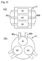
- FIG. 1 is a view showing an example of a Pen junction light emitting device lighting apparatus according to the present disclosure
- FIG. 2 is a view showing examples of the light emitting device package shown in FIG.
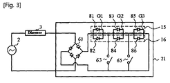
- FIG. 3 is a view illustrating an example of an electrical connection of a PJ junction lighting device according to the present disclosure
- FIG. 4 is a view for explaining a change in the AC voltage according to the application of the dimmer
- FIG. 6 is a view illustrating an example of use of a PJJ lighting device according to the present disclosure
- FIG. 7 is a cross-sectional view taken along the line II ′ of FIG. 6;
- FIG. 8 is a view showing another example of a PEN junction light emitting device lighting device according to the present disclosure.
- FIG. 1 is a view illustrating an example of a PJJ lighting device according to the present disclosure.
- FIG. 2 is a diagram illustrating examples of the light emitting device package illustrated in FIG. 1.
- 3 is a view showing an example of the electrical connection of the PIE junction light emitting device lighting apparatus according to the present disclosure.
- the PJJ lighting device 10 includes a power supply board 21, a plurality of PJPCs 81, 82, 83, 84, 85, 86, a first switch 63, and a second switch 65. And a rectifier circuit 61 of a bridge diode and a dimmer 3.
- the power transmission board 21 is, for example, a printed circuit board.
- the power transmission board 21 may include a metal layer, a wiring layer, and a connector 23 for heat dissipation.
- the wiring layer is formed on the metal layer and may include an insulating layer for insulating the wiring and the wiring.
- the shape of the power transmission board 21 may be changed into various shapes such as a disc, a rectangular plate, and a straight rod according to an example in which the PEN lighting device 10 is used.
- the connectors 23 may be provided at respective short side edges of the substantially rectangular power supply board 21 facing each other, and power is input to the connector 23 from the outside.
- the connection cable 40 (see FIG. 5) is coupled to the connector 23 to apply the transferred power to the connector 23.
- the plurality of PJ LED devices 10 may be electrically connected to each other by a connection cable 40.
- the PEN junction light emitting devices 81, 82, 83, 84, 85, and 86 emit light by power supplied by being mounted on the power transmission board 21.
- the PEN junction LED is a representative example of a light emitting diode (LED), and in addition to the laser diode (LD). A plurality of boundaries are defined on the power transmission board 21.
- the boundary is a unit in which the plurality of PJ LEDs 81, 82, 83, 84, 85, 86 are arranged.
- the boundary is a plurality of PJ LEDs 81, 82, 83. , 84, 85, and 86 are integrally provided light emitting device packages 15 and 16.
- the number and arrangement of the light emitting device packages 15 and 16 may be changed according to the type and use of the PEN-junction light emitting device lighting device 10.
- the light emitting device packages 15 and 16 are arranged in two rows. The case is illustrated.
- FIG. 3 shows the electrical connection between the first light emitting device package 15, the second light emitting device package 16, and the power transmission board 21 on behalf of the light emitting device packages 15 and 16 of the first row and the second row. Giving.
- the number of groups may vary depending on the number of PN-junction light emitting elements included in one boundary. For example, as illustrated in FIGS. 1 and 2, in the first light emitting device package 15, the PEN-junction light emitting device 81 of the first group G1 and the PEN-junction light emission of the second group G2 are provided.
- the device 83 and the Pen junction light emitting device 85 of the third group G3 are positioned.
- the PJJ light emitting device 82 of the first group G1, the PJJ light emitting device 84 of the second group G2, and the PJJ light emitting of the third group G3 are included in the second light emitting device package 16.
- Element 86 is located.
- three PN-junction light emitting devices 81, 82, 83, 84, 85, and 86 located in the first light emitting device package 15 and the second light emitting device package 16, respectively, are shown in FIG. 2.
- the input lead wire 80a and the output lead wire 80b are independently connected.
- the first group G1, the second group G2, and the third group G3 are connected in series as shown in FIG. 3.
- Piene junction light emitting devices belonging to the same group may be connected in parallel or in series with each other, and FIG. 3 illustrates a case where they are connected in parallel.
- the first switch 63 is connected between the first group G1 and the second group G2, and the second switch 65 is connected between the second group G2 and the third group G3. It is.
- the first switch 63 is turned on when the supplied alternating current is the first voltage, so that the first switch 63 of the first group G1 is located in the first light emitting device package 15 and the second light emitting device package 16.
- the light emitting diodes 81 and 82 emit light and when the supplied alternating current becomes a second voltage higher than the first voltage, the light emitting diodes 83 and 84 of the second group G2 emit light. in the off) state.
- the second switch 65 is turned on in a state where the supplied alternating current becomes a second voltage and the first switch 63 is turned off. 83, 84).
- the PJ LEDs connected in series may be arranged in both directions to alternately drive the PJ LEDs arranged in different directions according to the change of the direction of the current.
- the PEN junction light emitting devices 81, 82, 83, 84, 85, and 86 may be arranged in one direction, and the PEN junction light emitting devices 81 and 82 may be formed using the rectifier circuit 61.
- 83, 84, 85, 86 can be provided in one direction.
- FIG. 4 is a view for explaining a change in the AC voltage according to the application of the dimmer.
- the dimmer 3 may adjust the brightness of the PJJ lighting device 10 by controlling the AC voltage.
- the PJ-junction light emitting devices 81 and 82 of the first group G1 may emit light.
- the first switch 63 when the AC voltage reaches V1, the PJ-junction light emitting devices 81 and 82 of the first group G1 may emit light.
- the first switch 63 when the AC voltage reaches V2, the PJ-junction light emitting devices 83 and 84 of the second group G2 may emit light.
- the first switch 63 is turned off and the second switch 65 is turned on. When it is turned on, light emission of the first group G1 and the second group G2 is possible.
- the PIE-connected light emitting devices 85 and 86 of the third group G3 may also emit light, and when the first switch 63 and the second switch 65 are turned off, Light emission of the first group G1, the second group G2, and the third group G3 is possible.
- the PEN junction light emitting device 81 belonging to the first group G1 when the maximum voltage is set by the dimmer 3 to a value between V2 and V3, light emission occurs only in the first group G1 and the second group G2, and the third group G3.
- the PEN junction light emitting device 81 belonging to the first group G1 the PEN junction light emitting device 83 belonging to the second group G2, and the PEN junction light emitting device 85 belonging to the third group G3.
- the P-junction light emitting device 82 belonging to the first group G1 and the P-junction light emitting device belonging to the second group G2 ( 84) and the Pen-junction light emitting device 86 belonging to the third group G3 is included in the second light emitting device package 16 which is the other boundary. Therefore, even though the third group G3 does not emit light due to dimming, light is emitted from both the first light emitting device package 15 and the second light emitting device package 16 which are positioned throughout the PEN lighting device 10. To lose.
- FIG. 5 is a diagram illustrating an example of the configuration of the switch illustrated in FIG. 3.
- FIG. 6 is a diagram illustrating an example of use of a PJJ lighting device according to the present disclosure.
- FIG. 7 is a cross-sectional view taken along the line II ′ of FIG. 6.
- the PJJ lighting device 10 may be housed in a case as illustrated in FIGS. 6 and 7 to form a lighting module 5.
- the case includes, for example, a lower cover 30 and an upper cover 50.
- the PEN-junction light emitting device illuminating device 10 is disposed.
- the lower cover 30 may be made of plastic, and the lower cover 30 may have a groove 31 into which the power transmission board 20 is inserted, as shown in FIG. 6. Screw fastening holes 33 are formed at the corners of the lower cover 30.
- the metal layer of the power transmission substrate 21 contacts the lower cover 30, and heat generated when the PEN junction light emitting device 15 emits light is radiated through the metal layer and the lower cover 30 of the power transmission substrate 21. .
- the lighting module 5 employing the PN-junction light emitting device illumination device 10 has a large amount of volume and weight since a separate heat sink having a heat dissipation fin or a heating blade is removed.
- the lower cover 30 may be made of heat dissipation plastic having excellent heat dissipation.
- the number of light emitting device packages 15 and 16 mounted on the power transmission board 21 can be reduced to suppress excessive rise in temperature.
- the upper cover 50 is positioned on the power transmission board 21 and coupled to the lower cover 30.
- the top cover 50 may include a bottom portion 51, an inclined portion 53, and a side portion 56 as shown in FIGS. 6 and 7.
- An opening 55 corresponding to the light emitting device packages 15 and 16 is formed at the bottom 51.
- the light emitting device packages 15 and 16 may be exposed by the openings 55 and inserted into the openings 55 as shown in FIG. 7.
- the inclined portion 53 extends from the edge of the bottom portion 51 and extends upward to form an inclination angle with the bottom portion 51, as shown in FIG.
- the inclined portion 53 corresponds to the edge of the power transmission substrate 21, and a space is formed between the power transmission substrate 21 and the inclined portion 53, so that the first switch 63 and the second switch 65 described above. ), A space for the rectifier circuit 61 and the dimmer 3 is provided.
- the side portion 56 extends downward from the top of the inclined portion 53 and is coupled to the lower cover 30.
- a fastening protrusion 54 is formed at the side portion 56, and a fastening hole into which the fastening protrusion 54 is inserted in a hook coupling manner may be formed in the lower cover 30.
- the upper cover 50 may have a screwing hole 57 corresponding to the lower cover 30.
- the transparent lens 70 is positioned on the upper cover 50, and a guide groove in which the transparent lens 70 is disposed is formed on the upper side of the side cover 56 of the upper cover 50.
- the transparent lens 70 shields and protects the light emitting device packages 15 and 16 from the outside.
- the transparent lens 70 may be made of a transparent plastic, and may transmit light from the PEN-junction light emitting device and adjust a direction of light.
- the heat sink is removed, and a separate driving substrate for driving the light emitting device packages 15 and 16 is removed, thereby making the slim and light lighting module ( 5) can be provided.
- FIG. 8 is a view showing another example of a PN junction light emitting device lighting apparatus according to the present disclosure.
- the PEN-junction light emitting device illumination device 310 illustrated in FIG. 8 includes the PEN-junction light emitting device illumination described in FIGS. 1 to 7 except that the plurality of light emitting modules 301 and 303 are electrically connected to form a circuit. It is substantially the same as the device 10. Therefore, duplicate descriptions are omitted.
- a plurality of light emitting device packages 315 are arranged on the first power transfer board 321 to constitute the first light emitting module 301.
- a plurality of PEN-junction light emitting devices are located, and the PEN-junction light emitting devices in the light emitting device are divided into a plurality of groups.
- a plurality of light emitting device packages 317 are arranged on the second power transmission substrate 322 to constitute the second light emitting module 303.
- connection cable 340 is coupled to the connector, and the first power transfer board 321 and the second power transfer board 322 are electrically connected by the connection cable 340. Accordingly, the PEN-junction light emitting device of the first group of the first light emitting module 301 and the PEN-junction light emitting device of the first group of the second light emitting module 303 may be connected in parallel. In addition, the P-junction light emitting device of the second group of the first light emitting module 301 and the P-junction light emitting device of the second group of the second light emitting module 303 may be connected in parallel.
- the first switch, the second switch, and the rectifier circuit may be provided on one of the first power transfer board 321 or the second power transfer board 322.
- the first switch is turned on when the supplied alternating current is at a first voltage to emit light of the first group of Pen-junction light emitting devices positioned on the first power transmission substrate 321 and the second power transmission substrate 322. Let's do it.
- the first power supply board 321 connected in series with the first group in a state in which the second switch is turned on while the supplied alternating current becomes a second voltage higher than the first voltage and the first switch is turned off.
- a second group of P-junction light emitting devices of the second power transmission substrate 322 emit light.
- a plurality of light emitting modules may be connected to configure lighting devices of various uses and types.
- a PEN junction light emitting device illuminating device wherein a plurality of PEN junction light emitting elements in a boundary are packaged in a light emitting element package, and a boundary is defined by a light emitting element package.
- a PJ junction light emitting device comprising three PIE junction light emitting devices forming one light emitting device package, and each PEN junction light emitting device is independently connected to an input lead wire and an output lead wire.
- the one PEN junction light emitting element located within the first boundary and the one PEN junction light emitting element located within the second boundary are connected in parallel, and in the second group, located within the first boundary.
- the other PEN junction light emitting device and the other PEN junction light emitting device positioned within the second boundary are connected in parallel.
- the PEN-junction light emitting devices may be connected in series or in parallel, but when connected in parallel, it is possible to provide a lighting device capable of more sensitively responding to dimming.
- the PEN-junction light emitting devices may be connected in series or in parallel, but when connected in parallel, it is possible to provide a lighting device capable of more sensitively responding to dimming.
- three PIE junction light emitting devices (light emission at 3V) are provided in a group, 9V is required in series but 3V is required in parallel, and it is possible to cope with the dimmer in 3V units instead of 9V units. .
- a group of Pn-junction light emitting devices can be added as necessary. For example, when only the first group of PEN light emitting devices and the second group of PEN light emitting devices are located within a boundary, only one first switch may be connected between the first group and the second group.
- a PN-junction light emitting device illumination device characterized in that the PNP junction light emitting element of the first group and the PNP junction light emitting element of the second group are located on the power transmission substrate at a distance from each other.
- the boundary may be formed by one package having a plurality of chips, by a plurality of chips formed on one substrate, or simply by arranging a plurality of chips or packages in one region. It is desirable to use one package to increase the intensity of integration and to consider the wiring required later.
- a lower cover located below the power transmission board; An upper cover positioned on the power transmission substrate, the upper cover having an opening exposing the PJ junction light emitting element; And a transparent lens positioned on the upper cover and transmitting the light from the PEN light emitting device.
- the lighting apparatus can emit light without restriction due to the change of the structure of the first switch or the like according to the introduction of the dimmer.
- the plurality of PN-junction light emitting devices positioned in the first light emitting module and the second light emitting module are packaged in a light emitting device package, and the plurality of PN-junction light emitting devices located in each light emitting device package are divided into a plurality of groups.
- Piene junction light emitting device illumination device characterized in that.
- the P-junction light emitting device of the first group of the first light emitting module and the P-junction light emitting device of the first group of the second light emitting module are connected in parallel, and the P-junction light emitting device of the second group of the first light emitting module A PJ junction light emitting device according to claim 2, wherein the PJ junction light emitting device of the second group of the second light emitting module is connected in parallel.
- the PEN-junction light emitting device illuminating device is integrated with the PEN junction light emitting device and the switch for driving the PEN junction light emitting device, so that a separate driving substrate is removed.
- the volume and weight of the lighting lamp employing the element lighting device is reduced.
- the device provided in the power transmission board does not have an electrolytic capacitor that is vulnerable to heat, thereby preventing deterioration of reliability such as life.
- the PEN-junction semiconductor light emitting device lighting apparatus can provide a lighting apparatus suitable for dimming and using alternating current.
- a separate heat sink is removed and the lower cover, the power transmission board, the top cover and the transparent lens have a compact coupling structure, so that the slim and light PEN lighting device An apparatus is provided.
Landscapes
- Engineering & Computer Science (AREA)
- General Engineering & Computer Science (AREA)
- Microelectronics & Electronic Packaging (AREA)
- Physics & Mathematics (AREA)
- Optics & Photonics (AREA)
- Circuit Arrangement For Electric Light Sources In General (AREA)
- Arrangement Of Elements, Cooling, Sealing, Or The Like Of Lighting Devices (AREA)
- Non-Portable Lighting Devices Or Systems Thereof (AREA)
Abstract
La présente invention porte sur un appareil d'éclairage comprenant des dispositifs d'émission de lumière à jonctions P-N. L'appareil d'éclairage comprenant des dispositifs d'émission de lumière à jonctions P-N comprend : une carte de transmission de puissance dans laquelle une pluralité de limites sont définies ; une pluralité de dispositifs d'émission de lumière à jonctions P-N disposés à l'intérieur de la pluralité de limites et divisés en une pluralité de groupes, respectivement ; et un premier commutateur disposé sur la carte de transmission de puissance, le premier commutateur étant activé lorsque le courant alternatif fourni est à une première tension de façon à permettre aux dispositifs d'émission de lumière à jonctions P-N du premier groupe disposés à l'intérieur de chacune des limites d'émettre de la lumière, et étant désactivé lorsqu'une seconde tension supérieure à la première tension est appliquée de façon à permettre aux dispositifs d'émission de lumière à jonctions P-N du second groupe, disposés à l'intérieur de chacune des limites et connectés à ceux du premier groupe en série, d'émettre de la lumière.
Priority Applications (1)
| Application Number | Priority Date | Filing Date | Title |
|---|---|---|---|
| CN201180002660.8A CN102812293B (zh) | 2011-02-25 | 2011-11-04 | Pn结发光元件照明装置 |
Applications Claiming Priority (2)
| Application Number | Priority Date | Filing Date | Title |
|---|---|---|---|
| KR1020110016997A KR101287901B1 (ko) | 2011-02-25 | 2011-02-25 | 피엔접합 발광소자 조명 장치 |
| KR10-2011-0016997 | 2011-02-25 |
Publications (1)
| Publication Number | Publication Date |
|---|---|
| WO2012115329A1 true WO2012115329A1 (fr) | 2012-08-30 |
Family
ID=46718499
Family Applications (1)
| Application Number | Title | Priority Date | Filing Date |
|---|---|---|---|
| PCT/KR2011/008363 WO2012115329A1 (fr) | 2011-02-25 | 2011-11-04 | Appareil d'éclairage comprenant des dispositifs d'émission de lumière à jonctions p-n |
Country Status (4)
| Country | Link |
|---|---|
| US (1) | US8492981B2 (fr) |
| KR (1) | KR101287901B1 (fr) |
| CN (1) | CN102812293B (fr) |
| WO (1) | WO2012115329A1 (fr) |
Families Citing this family (5)
| Publication number | Priority date | Publication date | Assignee | Title |
|---|---|---|---|---|
| TWI434617B (zh) * | 2011-01-28 | 2014-04-11 | Analog Integrations Corp | 可提高電能轉換效率的驅動電路與其驅動方法 |
| CN102769961B (zh) * | 2011-05-05 | 2015-03-18 | 光宝电子(广州)有限公司 | 交流发光装置 |
| WO2013115439A1 (fr) * | 2012-02-02 | 2013-08-08 | 주식회사 포스코엘이디 | Dissipateur thermique et dispositif d'éclairage à del incluant ledit dissipateur |
| US8981668B2 (en) * | 2013-03-08 | 2015-03-17 | LT Lighting (Taiwan) Corp. | Demand-side initiated dimmable LED lamp |
| US20160066382A1 (en) * | 2014-08-27 | 2016-03-03 | Bridgelux, Inc. | Light emitting apparatus comprising individually controlled light emitting circuits on an integrated circuit |
Citations (4)
| Publication number | Priority date | Publication date | Assignee | Title |
|---|---|---|---|---|
| JP2008218043A (ja) * | 2007-02-28 | 2008-09-18 | Sharp Corp | Led駆動回路、及びled発光装置 |
| KR20090127208A (ko) * | 2008-06-07 | 2009-12-10 | 심현섭 | 교류전원에 의해 구동되는 알지비 컬러 엘이디 모듈 |
| KR20100009201A (ko) * | 2008-07-18 | 2010-01-27 | 안철용 | Led로 구성된 조립식 조명등 |
| KR20100121816A (ko) * | 2009-05-11 | 2010-11-19 | 엘지전자 주식회사 | Led 구동회로 및 그 구동방법 |
Family Cites Families (8)
| Publication number | Priority date | Publication date | Assignee | Title |
|---|---|---|---|---|
| US5457450A (en) * | 1993-04-29 | 1995-10-10 | R & M Deese Inc. | LED traffic signal light with automatic low-line voltage compensating circuit |
| JP3498290B1 (ja) * | 2002-12-19 | 2004-02-16 | 俊二 岸村 | 白色led照明装置 |
| US7081722B1 (en) * | 2005-02-04 | 2006-07-25 | Kimlong Huynh | Light emitting diode multiphase driver circuit and method |
| KR101186617B1 (ko) | 2006-02-21 | 2012-09-27 | 엘지이노텍 주식회사 | 엘이디 드라이브의 웨이브 노이즈 방지 장치 |
| US20110031889A1 (en) | 2008-05-09 | 2011-02-10 | Shim Hyun-Seop | Ac-powered led lighting system |
| KR20100052629A (ko) | 2008-11-11 | 2010-05-20 | 에프씨반도체 주식회사 | Led 조명등 |
| KR100926040B1 (ko) | 2009-05-19 | 2009-11-11 | 주식회사 케이디파워 | Led 조명등 |
| CN102169878B (zh) * | 2010-02-26 | 2013-02-20 | 旭丽电子(广州)有限公司 | 拼接式发光二极管模块 |
-
2011
- 2011-02-25 KR KR1020110016997A patent/KR101287901B1/ko not_active IP Right Cessation
- 2011-04-07 US US13/081,625 patent/US8492981B2/en not_active Expired - Fee Related
- 2011-11-04 WO PCT/KR2011/008363 patent/WO2012115329A1/fr active Application Filing
- 2011-11-04 CN CN201180002660.8A patent/CN102812293B/zh not_active Expired - Fee Related
Patent Citations (4)
| Publication number | Priority date | Publication date | Assignee | Title |
|---|---|---|---|---|
| JP2008218043A (ja) * | 2007-02-28 | 2008-09-18 | Sharp Corp | Led駆動回路、及びled発光装置 |
| KR20090127208A (ko) * | 2008-06-07 | 2009-12-10 | 심현섭 | 교류전원에 의해 구동되는 알지비 컬러 엘이디 모듈 |
| KR20100009201A (ko) * | 2008-07-18 | 2010-01-27 | 안철용 | Led로 구성된 조립식 조명등 |
| KR20100121816A (ko) * | 2009-05-11 | 2010-11-19 | 엘지전자 주식회사 | Led 구동회로 및 그 구동방법 |
Also Published As
| Publication number | Publication date |
|---|---|
| CN102812293B (zh) | 2015-03-04 |
| KR20120097657A (ko) | 2012-09-05 |
| US8492981B2 (en) | 2013-07-23 |
| US20120217891A1 (en) | 2012-08-30 |
| CN102812293A (zh) | 2012-12-05 |
| KR101287901B1 (ko) | 2013-07-18 |
Similar Documents
| Publication | Publication Date | Title |
|---|---|---|
| WO2010036067A2 (fr) | Appareil électroluminescent | |
| US9271354B2 (en) | Lighting source and lighting apparatus | |
| WO2016190644A1 (fr) | Dispositif electroluminescent et lampe de véhicule comprenant celui-ci | |
| WO2012115329A1 (fr) | Appareil d'éclairage comprenant des dispositifs d'émission de lumière à jonctions p-n | |
| WO2013005971A2 (fr) | Dispositif d'éclairage | |
| WO2012091258A1 (fr) | Alimentation électrique | |
| JP5793050B2 (ja) | 電源モジュール、led照明ユニット、led照明装置、および、led照明システム | |
| WO2018106052A1 (fr) | Dispositif d'éclairage et lampe pour automobile le comprenant | |
| EP2772681B1 (fr) | Dispositif d'éclairage | |
| WO2013039317A2 (fr) | Moteur d'éclairage à diodes électroluminescentes qui adopte une unité de diffusion de type stalactite | |
| WO2012115327A1 (fr) | Appareil d'éclairage ayant un élément émetteur de lumière à semi-conducteurs à jonction pn et procédé d'éclairage de celui-ci | |
| WO2019139328A1 (fr) | Dispositif d'éclairage | |
| WO2016140464A1 (fr) | Module de conditionnement de diode électroluminescente (del) comprenant une puce à courant constant intégrée | |
| WO2012115328A1 (fr) | Appareil d'éclairage comprenant un dispositif émetteur de lumière à jonction p-n | |
| TWI420048B (zh) | 光源模組 | |
| WO2010055983A1 (fr) | Module d’éclairage à del | |
| CN105546363A (zh) | 发光装置 | |
| US7946731B1 (en) | Power LED channel letter lighting module | |
| WO2014209055A1 (fr) | Appareil d'éclairage | |
| KR20130026785A (ko) | Dsp를 이용한 led 구동 장치 | |
| WO2017191941A1 (fr) | Appareil d'éclairage | |
| WO2013070025A1 (fr) | Appareil d'éclairage à led | |
| WO2014046439A1 (fr) | Barre à del | |
| WO2014133214A1 (fr) | Ampoule à del utilisant un circuit d'attaque de del à dissipation thermique | |
| WO2019146933A1 (fr) | Dispositif d'éclairage |
Legal Events
| Date | Code | Title | Description |
|---|---|---|---|
| WWE | Wipo information: entry into national phase |
Ref document number: 201180002660.8 Country of ref document: CN |
|
| 121 | Ep: the epo has been informed by wipo that ep was designated in this application |
Ref document number: 11859638 Country of ref document: EP Kind code of ref document: A1 |
|
| NENP | Non-entry into the national phase |
Ref country code: DE |
|
| 122 | Ep: pct application non-entry in european phase |
Ref document number: 11859638 Country of ref document: EP Kind code of ref document: A1 |