WO2012115329A1 - Lighting apparatus comprising p-n junction light-emitting devices - Google Patents
Lighting apparatus comprising p-n junction light-emitting devices Download PDFInfo
- Publication number
- WO2012115329A1 WO2012115329A1 PCT/KR2011/008363 KR2011008363W WO2012115329A1 WO 2012115329 A1 WO2012115329 A1 WO 2012115329A1 KR 2011008363 W KR2011008363 W KR 2011008363W WO 2012115329 A1 WO2012115329 A1 WO 2012115329A1
- Authority
- WO
- WIPO (PCT)
- Prior art keywords
- light emitting
- junction
- group
- emitting device
- pen
- Prior art date
Links
Images


Classifications
-
- H—ELECTRICITY
- H05—ELECTRIC TECHNIQUES NOT OTHERWISE PROVIDED FOR
- H05B—ELECTRIC HEATING; ELECTRIC LIGHT SOURCES NOT OTHERWISE PROVIDED FOR; CIRCUIT ARRANGEMENTS FOR ELECTRIC LIGHT SOURCES, IN GENERAL
- H05B45/00—Circuit arrangements for operating light-emitting diodes [LED]
- H05B45/40—Details of LED load circuits
- H05B45/44—Details of LED load circuits with an active control inside an LED matrix
- H05B45/48—Details of LED load circuits with an active control inside an LED matrix having LEDs organised in strings and incorporating parallel shunting devices
-
- F—MECHANICAL ENGINEERING; LIGHTING; HEATING; WEAPONS; BLASTING
- F21—LIGHTING
- F21K—NON-ELECTRIC LIGHT SOURCES USING LUMINESCENCE; LIGHT SOURCES USING ELECTROCHEMILUMINESCENCE; LIGHT SOURCES USING CHARGES OF COMBUSTIBLE MATERIAL; LIGHT SOURCES USING SEMICONDUCTOR DEVICES AS LIGHT-GENERATING ELEMENTS; LIGHT SOURCES NOT OTHERWISE PROVIDED FOR
- F21K9/00—Light sources using semiconductor devices as light-generating elements, e.g. using light-emitting diodes [LED] or lasers
- F21K9/60—Optical arrangements integrated in the light source, e.g. for improving the colour rendering index or the light extraction
-
- F—MECHANICAL ENGINEERING; LIGHTING; HEATING; WEAPONS; BLASTING
- F21—LIGHTING
- F21S—NON-PORTABLE LIGHTING DEVICES; SYSTEMS THEREOF; VEHICLE LIGHTING DEVICES SPECIALLY ADAPTED FOR VEHICLE EXTERIORS
- F21S2/00—Systems of lighting devices, not provided for in main groups F21S4/00 - F21S10/00 or F21S19/00, e.g. of modular construction
- F21S2/005—Systems of lighting devices, not provided for in main groups F21S4/00 - F21S10/00 or F21S19/00, e.g. of modular construction of modular construction
-
- F—MECHANICAL ENGINEERING; LIGHTING; HEATING; WEAPONS; BLASTING
- F21—LIGHTING
- F21V—FUNCTIONAL FEATURES OR DETAILS OF LIGHTING DEVICES OR SYSTEMS THEREOF; STRUCTURAL COMBINATIONS OF LIGHTING DEVICES WITH OTHER ARTICLES, NOT OTHERWISE PROVIDED FOR
- F21V23/00—Arrangement of electric circuit elements in or on lighting devices
- F21V23/003—Arrangement of electric circuit elements in or on lighting devices the elements being electronics drivers or controllers for operating the light source, e.g. for a LED array
- F21V23/004—Arrangement of electric circuit elements in or on lighting devices the elements being electronics drivers or controllers for operating the light source, e.g. for a LED array arranged on a substrate, e.g. a printed circuit board
- F21V23/005—Arrangement of electric circuit elements in or on lighting devices the elements being electronics drivers or controllers for operating the light source, e.g. for a LED array arranged on a substrate, e.g. a printed circuit board the substrate is supporting also the light source
-
- F—MECHANICAL ENGINEERING; LIGHTING; HEATING; WEAPONS; BLASTING
- F21—LIGHTING
- F21V—FUNCTIONAL FEATURES OR DETAILS OF LIGHTING DEVICES OR SYSTEMS THEREOF; STRUCTURAL COMBINATIONS OF LIGHTING DEVICES WITH OTHER ARTICLES, NOT OTHERWISE PROVIDED FOR
- F21V23/00—Arrangement of electric circuit elements in or on lighting devices
- F21V23/06—Arrangement of electric circuit elements in or on lighting devices the elements being coupling devices, e.g. connectors
-
- H—ELECTRICITY
- H05—ELECTRIC TECHNIQUES NOT OTHERWISE PROVIDED FOR
- H05B—ELECTRIC HEATING; ELECTRIC LIGHT SOURCES NOT OTHERWISE PROVIDED FOR; CIRCUIT ARRANGEMENTS FOR ELECTRIC LIGHT SOURCES, IN GENERAL
- H05B45/00—Circuit arrangements for operating light-emitting diodes [LED]
- H05B45/30—Driver circuits
- H05B45/37—Converter circuits
-
- F—MECHANICAL ENGINEERING; LIGHTING; HEATING; WEAPONS; BLASTING
- F21—LIGHTING
- F21Y—INDEXING SCHEME ASSOCIATED WITH SUBCLASSES F21K, F21L, F21S and F21V, RELATING TO THE FORM OR THE KIND OF THE LIGHT SOURCES OR OF THE COLOUR OF THE LIGHT EMITTED
- F21Y2115/00—Light-generating elements of semiconductor light sources
- F21Y2115/10—Light-emitting diodes [LED]
Definitions
- the present disclosure relates generally to a PIE-junction light emitting device illumination device, and more particularly to a PIE-junction light emitting device illumination device having reduced volume and weight.
- a light emitting diode module in which a plurality of light emitting diodes are mounted on a power transmission board is used as a light source.
- the light emitting diode has advantages such as small size, low power consumption, and excellent control characteristics, so that the light emitting diode lighting device can be manufactured slim and light.
- a conventional LED lighting device has a separate driving substrate for driving a heat sink or LED module for heat dissipation. Elements such as heat sinks and driving substrates make it difficult to make the light emitting diode lighting device slim and light.
- the driving substrate may be provided with an A / D converter to provide a DC power source, and the A / D converter includes a transformer coil for stepping down alternating current. Since the transformer coil is disposed at a considerable size in the driving substrate, there is a problem in that a product to which the transformer is applied is enlarged.
- SMPS switching mode power supply
- the light emitting diode module includes a plurality of light emitting diodes, the total current capacity is increased, so that an electrolytic capacitor is used as a component in a conventional light emitting diode driving circuit. While such an electrolytic capacitor is suitable for a circuit having a large capacitance, there is a problem in that the reliability of the circuit is deteriorated because the frequency characteristic is bad and the deterioration is relatively high. In particular, when the electrolytic capacitor is mounted on the power transmission board together with the light emitting diode, the life of the electrolytic capacitor is further shortened due to heat due to the light emission of the light emitting diode. In addition, in a circuit in which a plurality of light emitting diodes are arranged, there is a problem of limiting the exterior design of the light emitting diode lighting apparatus as the volume of the inductor and the capacitor increases.
- a conventional lighting device in which columns are connected in parallel by arranging a plurality of PN-junction light emitting devices in both directions directly to an AC power source without a separate driving circuit.
- the necessary voltage is controlled through a resistor, and when the positive voltage is applied, the P-junction light emitting device in one direction emits light, and when the negative voltage is applied, the P-junction light emitting device in the opposite direction emits light. .
- Such a lighting device has the advantage of simply implementing a PEN-junction light emitting device lighting device without a separate driving circuit for converting alternating current into direct current, but causes a problem in the use of a dimmer (see FIG. 2). For example, if 10V is required to drive a series-connected PN-junction light emitting device, if it is dimmed to 5V, current will not be conducted. In the case of using a dimmer of the conduction time on / off method, the light emitting time is limited because the PEN junction light emitting element does not emit light at 10V or less basically. can do.
- a power transmission board on which a plurality of boundaries are defined; A plurality of PN-junction light emitting elements positioned within each boundary and divided into a plurality of groups; And provided to the power transmission substrate, and when the supplied alternating current is the first voltage, the light is turned on to emit light of the first group of PEN junction light emitting elements located within each boundary, and the supplied alternating current is higher than the first voltage. And a first switch which is in an off state when the second group of Pn-junction light emitting devices positioned within each boundary connected in series to the first group at a second voltage is emitted.
- a light emitting device illumination device is provided.
- a first light emitting module including a first power transfer substrate and a plurality of PJ-junction light emitting elements provided in the first power transfer substrate;
- a second light emitting module including a second power transfer substrate electrically connected to the first power transfer substrate, and a plurality of PJ junction light emitting elements provided on the second power transfer substrate; And when the supplied alternating current is at the first voltage, the device is turned on to emit light of the first group of PEN junction light emitting devices positioned on the first power supply board and the second power supply board, and the supplied alternating current is the first voltage.
- a first switch which is in an off state when the first power transfer board connected to the first group in series with a higher second voltage and the PEN-junction light emitting devices of the second group of the second power transfer board are emitted;
- a PJ junction light emitting device lighting apparatus comprising a.
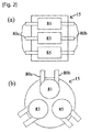
- FIG. 1 is a view showing an example of a Pen junction light emitting device lighting apparatus according to the present disclosure
- FIG. 2 is a view showing examples of the light emitting device package shown in FIG.
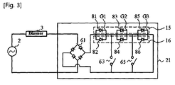
- FIG. 3 is a view illustrating an example of an electrical connection of a PJ junction lighting device according to the present disclosure
- FIG. 4 is a view for explaining a change in the AC voltage according to the application of the dimmer
- FIG. 6 is a view illustrating an example of use of a PJJ lighting device according to the present disclosure
- FIG. 7 is a cross-sectional view taken along the line II ′ of FIG. 6;
- FIG. 8 is a view showing another example of a PEN junction light emitting device lighting device according to the present disclosure.
- FIG. 1 is a view illustrating an example of a PJJ lighting device according to the present disclosure.
- FIG. 2 is a diagram illustrating examples of the light emitting device package illustrated in FIG. 1.
- 3 is a view showing an example of the electrical connection of the PIE junction light emitting device lighting apparatus according to the present disclosure.
- the PJJ lighting device 10 includes a power supply board 21, a plurality of PJPCs 81, 82, 83, 84, 85, 86, a first switch 63, and a second switch 65. And a rectifier circuit 61 of a bridge diode and a dimmer 3.
- the power transmission board 21 is, for example, a printed circuit board.
- the power transmission board 21 may include a metal layer, a wiring layer, and a connector 23 for heat dissipation.
- the wiring layer is formed on the metal layer and may include an insulating layer for insulating the wiring and the wiring.
- the shape of the power transmission board 21 may be changed into various shapes such as a disc, a rectangular plate, and a straight rod according to an example in which the PEN lighting device 10 is used.
- the connectors 23 may be provided at respective short side edges of the substantially rectangular power supply board 21 facing each other, and power is input to the connector 23 from the outside.
- the connection cable 40 (see FIG. 5) is coupled to the connector 23 to apply the transferred power to the connector 23.
- the plurality of PJ LED devices 10 may be electrically connected to each other by a connection cable 40.
- the PEN junction light emitting devices 81, 82, 83, 84, 85, and 86 emit light by power supplied by being mounted on the power transmission board 21.
- the PEN junction LED is a representative example of a light emitting diode (LED), and in addition to the laser diode (LD). A plurality of boundaries are defined on the power transmission board 21.
- the boundary is a unit in which the plurality of PJ LEDs 81, 82, 83, 84, 85, 86 are arranged.
- the boundary is a plurality of PJ LEDs 81, 82, 83. , 84, 85, and 86 are integrally provided light emitting device packages 15 and 16.
- the number and arrangement of the light emitting device packages 15 and 16 may be changed according to the type and use of the PEN-junction light emitting device lighting device 10.
- the light emitting device packages 15 and 16 are arranged in two rows. The case is illustrated.
- FIG. 3 shows the electrical connection between the first light emitting device package 15, the second light emitting device package 16, and the power transmission board 21 on behalf of the light emitting device packages 15 and 16 of the first row and the second row. Giving.
- the number of groups may vary depending on the number of PN-junction light emitting elements included in one boundary. For example, as illustrated in FIGS. 1 and 2, in the first light emitting device package 15, the PEN-junction light emitting device 81 of the first group G1 and the PEN-junction light emission of the second group G2 are provided.
- the device 83 and the Pen junction light emitting device 85 of the third group G3 are positioned.
- the PJJ light emitting device 82 of the first group G1, the PJJ light emitting device 84 of the second group G2, and the PJJ light emitting of the third group G3 are included in the second light emitting device package 16.
- Element 86 is located.
- three PN-junction light emitting devices 81, 82, 83, 84, 85, and 86 located in the first light emitting device package 15 and the second light emitting device package 16, respectively, are shown in FIG. 2.
- the input lead wire 80a and the output lead wire 80b are independently connected.
- the first group G1, the second group G2, and the third group G3 are connected in series as shown in FIG. 3.
- Piene junction light emitting devices belonging to the same group may be connected in parallel or in series with each other, and FIG. 3 illustrates a case where they are connected in parallel.
- the first switch 63 is connected between the first group G1 and the second group G2, and the second switch 65 is connected between the second group G2 and the third group G3. It is.
- the first switch 63 is turned on when the supplied alternating current is the first voltage, so that the first switch 63 of the first group G1 is located in the first light emitting device package 15 and the second light emitting device package 16.
- the light emitting diodes 81 and 82 emit light and when the supplied alternating current becomes a second voltage higher than the first voltage, the light emitting diodes 83 and 84 of the second group G2 emit light. in the off) state.
- the second switch 65 is turned on in a state where the supplied alternating current becomes a second voltage and the first switch 63 is turned off. 83, 84).
- the PJ LEDs connected in series may be arranged in both directions to alternately drive the PJ LEDs arranged in different directions according to the change of the direction of the current.
- the PEN junction light emitting devices 81, 82, 83, 84, 85, and 86 may be arranged in one direction, and the PEN junction light emitting devices 81 and 82 may be formed using the rectifier circuit 61.
- 83, 84, 85, 86 can be provided in one direction.
- FIG. 4 is a view for explaining a change in the AC voltage according to the application of the dimmer.
- the dimmer 3 may adjust the brightness of the PJJ lighting device 10 by controlling the AC voltage.
- the PJ-junction light emitting devices 81 and 82 of the first group G1 may emit light.
- the first switch 63 when the AC voltage reaches V1, the PJ-junction light emitting devices 81 and 82 of the first group G1 may emit light.
- the first switch 63 when the AC voltage reaches V2, the PJ-junction light emitting devices 83 and 84 of the second group G2 may emit light.
- the first switch 63 is turned off and the second switch 65 is turned on. When it is turned on, light emission of the first group G1 and the second group G2 is possible.
- the PIE-connected light emitting devices 85 and 86 of the third group G3 may also emit light, and when the first switch 63 and the second switch 65 are turned off, Light emission of the first group G1, the second group G2, and the third group G3 is possible.
- the PEN junction light emitting device 81 belonging to the first group G1 when the maximum voltage is set by the dimmer 3 to a value between V2 and V3, light emission occurs only in the first group G1 and the second group G2, and the third group G3.
- the PEN junction light emitting device 81 belonging to the first group G1 the PEN junction light emitting device 83 belonging to the second group G2, and the PEN junction light emitting device 85 belonging to the third group G3.
- the P-junction light emitting device 82 belonging to the first group G1 and the P-junction light emitting device belonging to the second group G2 ( 84) and the Pen-junction light emitting device 86 belonging to the third group G3 is included in the second light emitting device package 16 which is the other boundary. Therefore, even though the third group G3 does not emit light due to dimming, light is emitted from both the first light emitting device package 15 and the second light emitting device package 16 which are positioned throughout the PEN lighting device 10. To lose.
- FIG. 5 is a diagram illustrating an example of the configuration of the switch illustrated in FIG. 3.
- FIG. 6 is a diagram illustrating an example of use of a PJJ lighting device according to the present disclosure.
- FIG. 7 is a cross-sectional view taken along the line II ′ of FIG. 6.
- the PJJ lighting device 10 may be housed in a case as illustrated in FIGS. 6 and 7 to form a lighting module 5.
- the case includes, for example, a lower cover 30 and an upper cover 50.
- the PEN-junction light emitting device illuminating device 10 is disposed.
- the lower cover 30 may be made of plastic, and the lower cover 30 may have a groove 31 into which the power transmission board 20 is inserted, as shown in FIG. 6. Screw fastening holes 33 are formed at the corners of the lower cover 30.
- the metal layer of the power transmission substrate 21 contacts the lower cover 30, and heat generated when the PEN junction light emitting device 15 emits light is radiated through the metal layer and the lower cover 30 of the power transmission substrate 21. .
- the lighting module 5 employing the PN-junction light emitting device illumination device 10 has a large amount of volume and weight since a separate heat sink having a heat dissipation fin or a heating blade is removed.
- the lower cover 30 may be made of heat dissipation plastic having excellent heat dissipation.
- the number of light emitting device packages 15 and 16 mounted on the power transmission board 21 can be reduced to suppress excessive rise in temperature.
- the upper cover 50 is positioned on the power transmission board 21 and coupled to the lower cover 30.
- the top cover 50 may include a bottom portion 51, an inclined portion 53, and a side portion 56 as shown in FIGS. 6 and 7.
- An opening 55 corresponding to the light emitting device packages 15 and 16 is formed at the bottom 51.
- the light emitting device packages 15 and 16 may be exposed by the openings 55 and inserted into the openings 55 as shown in FIG. 7.
- the inclined portion 53 extends from the edge of the bottom portion 51 and extends upward to form an inclination angle with the bottom portion 51, as shown in FIG.
- the inclined portion 53 corresponds to the edge of the power transmission substrate 21, and a space is formed between the power transmission substrate 21 and the inclined portion 53, so that the first switch 63 and the second switch 65 described above. ), A space for the rectifier circuit 61 and the dimmer 3 is provided.
- the side portion 56 extends downward from the top of the inclined portion 53 and is coupled to the lower cover 30.
- a fastening protrusion 54 is formed at the side portion 56, and a fastening hole into which the fastening protrusion 54 is inserted in a hook coupling manner may be formed in the lower cover 30.
- the upper cover 50 may have a screwing hole 57 corresponding to the lower cover 30.
- the transparent lens 70 is positioned on the upper cover 50, and a guide groove in which the transparent lens 70 is disposed is formed on the upper side of the side cover 56 of the upper cover 50.
- the transparent lens 70 shields and protects the light emitting device packages 15 and 16 from the outside.
- the transparent lens 70 may be made of a transparent plastic, and may transmit light from the PEN-junction light emitting device and adjust a direction of light.
- the heat sink is removed, and a separate driving substrate for driving the light emitting device packages 15 and 16 is removed, thereby making the slim and light lighting module ( 5) can be provided.
- FIG. 8 is a view showing another example of a PN junction light emitting device lighting apparatus according to the present disclosure.
- the PEN-junction light emitting device illumination device 310 illustrated in FIG. 8 includes the PEN-junction light emitting device illumination described in FIGS. 1 to 7 except that the plurality of light emitting modules 301 and 303 are electrically connected to form a circuit. It is substantially the same as the device 10. Therefore, duplicate descriptions are omitted.
- a plurality of light emitting device packages 315 are arranged on the first power transfer board 321 to constitute the first light emitting module 301.
- a plurality of PEN-junction light emitting devices are located, and the PEN-junction light emitting devices in the light emitting device are divided into a plurality of groups.
- a plurality of light emitting device packages 317 are arranged on the second power transmission substrate 322 to constitute the second light emitting module 303.
- connection cable 340 is coupled to the connector, and the first power transfer board 321 and the second power transfer board 322 are electrically connected by the connection cable 340. Accordingly, the PEN-junction light emitting device of the first group of the first light emitting module 301 and the PEN-junction light emitting device of the first group of the second light emitting module 303 may be connected in parallel. In addition, the P-junction light emitting device of the second group of the first light emitting module 301 and the P-junction light emitting device of the second group of the second light emitting module 303 may be connected in parallel.
- the first switch, the second switch, and the rectifier circuit may be provided on one of the first power transfer board 321 or the second power transfer board 322.
- the first switch is turned on when the supplied alternating current is at a first voltage to emit light of the first group of Pen-junction light emitting devices positioned on the first power transmission substrate 321 and the second power transmission substrate 322. Let's do it.
- the first power supply board 321 connected in series with the first group in a state in which the second switch is turned on while the supplied alternating current becomes a second voltage higher than the first voltage and the first switch is turned off.
- a second group of P-junction light emitting devices of the second power transmission substrate 322 emit light.
- a plurality of light emitting modules may be connected to configure lighting devices of various uses and types.
- a PEN junction light emitting device illuminating device wherein a plurality of PEN junction light emitting elements in a boundary are packaged in a light emitting element package, and a boundary is defined by a light emitting element package.
- a PJ junction light emitting device comprising three PIE junction light emitting devices forming one light emitting device package, and each PEN junction light emitting device is independently connected to an input lead wire and an output lead wire.
- the one PEN junction light emitting element located within the first boundary and the one PEN junction light emitting element located within the second boundary are connected in parallel, and in the second group, located within the first boundary.
- the other PEN junction light emitting device and the other PEN junction light emitting device positioned within the second boundary are connected in parallel.
- the PEN-junction light emitting devices may be connected in series or in parallel, but when connected in parallel, it is possible to provide a lighting device capable of more sensitively responding to dimming.
- the PEN-junction light emitting devices may be connected in series or in parallel, but when connected in parallel, it is possible to provide a lighting device capable of more sensitively responding to dimming.
- three PIE junction light emitting devices (light emission at 3V) are provided in a group, 9V is required in series but 3V is required in parallel, and it is possible to cope with the dimmer in 3V units instead of 9V units. .
- a group of Pn-junction light emitting devices can be added as necessary. For example, when only the first group of PEN light emitting devices and the second group of PEN light emitting devices are located within a boundary, only one first switch may be connected between the first group and the second group.
- a PN-junction light emitting device illumination device characterized in that the PNP junction light emitting element of the first group and the PNP junction light emitting element of the second group are located on the power transmission substrate at a distance from each other.
- the boundary may be formed by one package having a plurality of chips, by a plurality of chips formed on one substrate, or simply by arranging a plurality of chips or packages in one region. It is desirable to use one package to increase the intensity of integration and to consider the wiring required later.
- a lower cover located below the power transmission board; An upper cover positioned on the power transmission substrate, the upper cover having an opening exposing the PJ junction light emitting element; And a transparent lens positioned on the upper cover and transmitting the light from the PEN light emitting device.
- the lighting apparatus can emit light without restriction due to the change of the structure of the first switch or the like according to the introduction of the dimmer.
- the plurality of PN-junction light emitting devices positioned in the first light emitting module and the second light emitting module are packaged in a light emitting device package, and the plurality of PN-junction light emitting devices located in each light emitting device package are divided into a plurality of groups.
- Piene junction light emitting device illumination device characterized in that.
- the P-junction light emitting device of the first group of the first light emitting module and the P-junction light emitting device of the first group of the second light emitting module are connected in parallel, and the P-junction light emitting device of the second group of the first light emitting module A PJ junction light emitting device according to claim 2, wherein the PJ junction light emitting device of the second group of the second light emitting module is connected in parallel.
- the PEN-junction light emitting device illuminating device is integrated with the PEN junction light emitting device and the switch for driving the PEN junction light emitting device, so that a separate driving substrate is removed.
- the volume and weight of the lighting lamp employing the element lighting device is reduced.
- the device provided in the power transmission board does not have an electrolytic capacitor that is vulnerable to heat, thereby preventing deterioration of reliability such as life.
- the PEN-junction semiconductor light emitting device lighting apparatus can provide a lighting apparatus suitable for dimming and using alternating current.
- a separate heat sink is removed and the lower cover, the power transmission board, the top cover and the transparent lens have a compact coupling structure, so that the slim and light PEN lighting device An apparatus is provided.
Abstract
The present invention relates to a lighting apparatus comprising P-N junction light-emitting devices. The lighting apparatus comprising P-N junction light-emitting devices includes: a power transmission board in which a plurality of boundaries are defined; a plurality of P-N junction light-emitting devices disposed within the plurality of boundaries and divided into a plurality of groups, respectively; and a first switch disposed on the power transmission board, the first switch being turned on when the supplied alternating current is a first voltage so as to enable the P-N junction light-emitting devices of the first group disposed within each of the boundaries to emit light, and being turned off when a second voltage greater than the first voltage is applied so as to enable the P-N junction light-emitting devices of the second group, disposed within each of the boundaries and connected to those of the first group in series, to emit light.
Description
본 개시는 전체적으로 피엔접합 발광소자 조명 장치에 관한 것으로, 특히 부피 및 무게가 감소된 피엔접합 발광소자 조명 장치에 관한 것이다.The present disclosure relates generally to a PIE-junction light emitting device illumination device, and more particularly to a PIE-junction light emitting device illumination device having reduced volume and weight.
여기서는, 본 개시에 관한 배경기술이 제공되며, 이들이 반드시 공지기술을 의미하는 것은 아니다(This section provides background information related to the present disclosure which is not necessarily prior art).This section provides background information related to the present disclosure which is not necessarily prior art.
피엔접합 발광소자 조명 장치에서 대표적으로 다수의 발광다이오드(Light Emitting Diode)가 전원전달기판에 실장된 발광다이오드 모듈이 광원으로 사용된다. 발광다이오드는 작은 크기, 낮은 소비전력 및 우수한 제어특성 등의 장점을 가지므로 발광다이오드 조명 장치도 슬림하고 가볍게 제조할 수 있는 장점이 있다. 그러나 통상적인 발광다이오드 조명 장치는 방열을 위한 히트싱크나 발광다이오드 모듈을 구동하기 위한 별도의 구동기판을 구비한다. 이러한 히트싱크나 구동기판과 같은 요소는 발광다이오드 조명 장치를 슬림하고 가볍게 제작하는 데에 어려움을 준다.In the PJJ lighting device, a light emitting diode module in which a plurality of light emitting diodes are mounted on a power transmission board is used as a light source. The light emitting diode has advantages such as small size, low power consumption, and excellent control characteristics, so that the light emitting diode lighting device can be manufactured slim and light. However, a conventional LED lighting device has a separate driving substrate for driving a heat sink or LED module for heat dissipation. Elements such as heat sinks and driving substrates make it difficult to make the light emitting diode lighting device slim and light.
예를 들어, 구동기판에는 직류전원을 제공하기 위해 A/D 컨버터가 구비될 수 있으며, A/D 컨버터는 교류를 강압하기 위한 트랜스 코일을 포함한다. 트랜스 코일은 구동기판에서 상당한 크기로 배치되기 때문에 이를 적용한 제품이 대형화되는 문제점이 있다.For example, the driving substrate may be provided with an A / D converter to provide a DC power source, and the A / D converter includes a transformer coil for stepping down alternating current. Since the transformer coil is disposed at a considerable size in the driving substrate, there is a problem in that a product to which the transformer is applied is enlarged.
상기와 같은 문제점을 해결하기 위해 최근에는 SMPS(Switching Mode Power Supply)라 호칭되는 전원공급장치가 적용된다. SMPS는 교류 주파수(50㎐~60㎐)를 직류로 변환하여 사용하며, 이에 따른 고난도의 기술이 필요하다.In order to solve the above problems, a power supply device called a switching mode power supply (SMPS) is recently applied. SMPS converts AC frequency (50Hz ~ 60Hz) into DC and uses high difficulty technology accordingly.
하지만, 종래의 SMPS를 이용한 LED 구동장치는, 고속 스위칭을 사용하기 때문에 노이즈가 많이 발생되어 노이즈 필터를 반드시 구성하여야 하고, 그 이외에도 회로 구성시 많은 부품을 사용하기 때문에 저렴한 비용으로 회로를 구성하기 어렵다. 또한, SMPS 자체도 LED 모듈의 크기에 대비하여 상당히 큰 크기이기 때문에 LED 모듈의 소형화에는 한계가 발생되어 제품 자체를 소형화하기 어려운 문제점이 있었다.However, in the conventional LED driver using SMPS, since high noise is generated, a lot of noise is generated, and a noise filter must be configured. Besides, many components are used in circuit construction, and thus it is difficult to construct a circuit at low cost. . In addition, since the SMPS itself is quite large compared to the size of the LED module, there is a problem in miniaturization of the LED module, which makes it difficult to miniaturize the product itself.
한편, 발광다이오드 모듈이 다수의 발광다이오드를 포함하므로 전체 전류 용량이 커져 종래의 발광다이오드 구동회로에는 전해 커패시터(electrolytic capacitor)를 부품으로 채용하고 있는 실정이다. 이와 같은 전해 커패시터는 큰 정전용량의 회로에 적합한 반면, 주파수 특성이 나쁘고, 경년열화가 비교적 높기 때문에 회로의 신뢰성이 저하되는 문제가 있다. 특히 전해 커패시터를 발광다이오드와 함께 전원전달기판에 실장하는 경우 발광다이오드의 발광으로 인한 열 때문에 전해 커패시터의 수명이 더욱 단축되는 문제점이 발생하였다. 또한, 다수의 발광다이오드가 배열된 회로에서는 인덕터와 커패시터의 부피가 커짐에 따라 발광다이오드 조명 장치의 외장 디자인에까지 제약을 주는 문제점이 있다.On the other hand, since the light emitting diode module includes a plurality of light emitting diodes, the total current capacity is increased, so that an electrolytic capacitor is used as a component in a conventional light emitting diode driving circuit. While such an electrolytic capacitor is suitable for a circuit having a large capacitance, there is a problem in that the reliability of the circuit is deteriorated because the frequency characteristic is bad and the deterioration is relatively high. In particular, when the electrolytic capacitor is mounted on the power transmission board together with the light emitting diode, the life of the electrolytic capacitor is further shortened due to heat due to the light emission of the light emitting diode. In addition, in a circuit in which a plurality of light emitting diodes are arranged, there is a problem of limiting the exterior design of the light emitting diode lighting apparatus as the volume of the inductor and the capacitor increases.
또한, 종래의 조명 장치는 일 예로 별도의 구동 회로 없이 교류 전원에 직접 복수의 피엔접합 발광소자를 양방향으로 배열하여 열들이 병렬연결되어 사용되는 경우가 개시되어 있다. 필요한 전압의 조절은 저항을 통해 이루어지며, 양(+)의 전압 인가시에 일 방향의 피엔접합 발광소자가 발광되고, 음(-)의 전압 인가시에 반대 방향의 피엔접합 발광소자가 발광된다.In addition, a conventional lighting device is disclosed in which columns are connected in parallel by arranging a plurality of PN-junction light emitting devices in both directions directly to an AC power source without a separate driving circuit. The necessary voltage is controlled through a resistor, and when the positive voltage is applied, the P-junction light emitting device in one direction emits light, and when the negative voltage is applied, the P-junction light emitting device in the opposite direction emits light. .
이러한 조명 장치는 교류를 직류로 전환하는 별도의 구동 회로 없이도 간단히 피엔접합 발광소자 조명 장치를 구현하는 이점을 가지지만, 조광기(Dimmer; 도 2 참조)의 사용에 문제점을 야기한다. 예를 들어 직렬연결된 피엔접합 발광소자의 구동에 10V가 필요한 경우에 5V로 조광된다면, 전류가 도통되지 않게 된다. 도통 시간을 on/off하는 방식의 조광기를 이용하는 경우에, 기본적으로 10V 이하에서 피엔접합 발광소자가 발광하지 않아 발광 시간이 제약되는데, 더하여 조광기에 의해 도통 시간이 제약되면 눈깜박임 등의 문제점을 야기할 수 있다.Such a lighting device has the advantage of simply implementing a PEN-junction light emitting device lighting device without a separate driving circuit for converting alternating current into direct current, but causes a problem in the use of a dimmer (see FIG. 2). For example, if 10V is required to drive a series-connected PN-junction light emitting device, if it is dimmed to 5V, current will not be conducted. In the case of using a dimmer of the conduction time on / off method, the light emitting time is limited because the PEN junction light emitting element does not emit light at 10V or less basically. can do.
이에 대하여 '발명의 실시를 위한 구체적인 내용'의 후단에 기술한다.This is described later in the section titled 'Details of the Invention.'
여기서는, 본 개시의 전체적인 요약(Summary)이 제공되며, 이것이 본 개시의 외연을 제한하는 것으로 이해되어서는 아니된다(This section provides a general summary of the disclosure and is not a comprehensive disclosure of its full scope or all of its features).This section provides a general summary of the disclosure and is not a comprehensive disclosure of its full scope or all, provided that this is a summary of the disclosure. of its features).
본 개시에 따른 일 태양에 의하면(According to one aspect of the present disclosure), 복수의 경계(boundary)가 정의된 전원전달기판; 각 경계 내에 위치하며 복수의 그룹으로 구분된 복수의 피엔접합 발광소자; 그리고 전원전달기판에 구비되며, 공급된 교류가 제1 전압일 때 온(on) 상태로 되어 각 경계 내에 위치하는 제1 그룹의 피엔접합 발광소자를 발광시키며, 공급된 교류가 제1 전압보다 높은 제2 전압으로 되어 제1 그룹에 직렬로 연결된 각 경계 내에 위치하는 제2 그룹의 피엔접합 발광소자가 발광될 때, 오프(off)된 상태인 제1 스위치;를 포함하는 것을 특징으로 하는 피엔접합 발광소자 조명 장치가 제공된다.According to one aspect of the present disclosure (According to one aspect of the present disclosure), a power transmission board on which a plurality of boundaries are defined; A plurality of PN-junction light emitting elements positioned within each boundary and divided into a plurality of groups; And provided to the power transmission substrate, and when the supplied alternating current is the first voltage, the light is turned on to emit light of the first group of PEN junction light emitting elements located within each boundary, and the supplied alternating current is higher than the first voltage. And a first switch which is in an off state when the second group of Pn-junction light emitting devices positioned within each boundary connected in series to the first group at a second voltage is emitted. A light emitting device illumination device is provided.
본 개시에 따른 다른 태양에 의하면(According to one aspect of the present disclosure), 제1 전원전달기판과, 제1 전원전달기판에 구비된 복수의 피엔접합 발광소자를 포함하는 제1 발광 모듈; 제1 전원전달기판과 전기적으로 연결되는 제2 전원전달기판과, 제2 전원전달기판 위에 구비된 복수의 피엔접합 발광소자를 포함하는 제2 발광 모듈; 그리고 공급된 교류가 제1 전압일 때 온(on) 상태로 되어 제1 전원전달기판 및 제2 전원전달기판 위에 위치하는 제1 그룹의 피엔접합 발광소자를 발광시키며, 공급된 교류가 제1 전압보다 높은 제2 전압으로 되어 제1 그룹에 직렬로 연결된 제1 전원전달기판 및 제2 전원전달기판의 제2 그룹의 피엔접합 발광소자가 발광될 때, 오프(off)된 상태인 제1 스위치;를 포함하는 것을 특징으로 하는 피엔접합 발광소자 조명 장치가 제공된다.According to another aspect of the present disclosure (According to one aspect of the present disclosure), a first light emitting module including a first power transfer substrate and a plurality of PJ-junction light emitting elements provided in the first power transfer substrate; A second light emitting module including a second power transfer substrate electrically connected to the first power transfer substrate, and a plurality of PJ junction light emitting elements provided on the second power transfer substrate; And when the supplied alternating current is at the first voltage, the device is turned on to emit light of the first group of PEN junction light emitting devices positioned on the first power supply board and the second power supply board, and the supplied alternating current is the first voltage. A first switch which is in an off state when the first power transfer board connected to the first group in series with a higher second voltage and the PEN-junction light emitting devices of the second group of the second power transfer board are emitted; Provided is a PJ junction light emitting device lighting apparatus comprising a.
이에 대하여 '발명의 실시를 위한 구체적인 내용'의 후단에 기술한다.This is described later in the section titled 'Details of the Invention.'
도 1은 본 개시에 따른 피엔접합 발광소자 조명 장치의 일 예를 나타내는 도면,1 is a view showing an example of a Pen junction light emitting device lighting apparatus according to the present disclosure;
도 2는 도 1에 도시된 발광소자 패키지의 예들을 나타내는 도면, 2 is a view showing examples of the light emitting device package shown in FIG.
도 3은 본 개시에 따른 피엔접합 발광소자 조명 장치의 전기적 연결의 일 예를 나타내는 도면,3 is a view illustrating an example of an electrical connection of a PJ junction lighting device according to the present disclosure;
도 4는 조광기의 적용에 따른 교류 전압의 변화를 설명하는 도면,4 is a view for explaining a change in the AC voltage according to the application of the dimmer,
도 5는 3에 도시된 스위치의 구성의 일 예를 나타내는 도면,5 is a view showing an example of the configuration of the switch shown in 3,
도 6은 본 개시에 따른 피엔접합 발광소자 조명 장치의 사용 예를 나타내는 도면,6 is a view illustrating an example of use of a PJJ lighting device according to the present disclosure;
도 7은 도 6에 도시된 I-I' 선을 따라 절단한 단면을 나타내는 도면,7 is a cross-sectional view taken along the line II ′ of FIG. 6;
도 8은 본 개시에 따른 피엔접합 발광소자 조명 장치의 다른 예를 나타내는 도면.8 is a view showing another example of a PEN junction light emitting device lighting device according to the present disclosure.
이하, 본 개시를 첨부된 도면을 참고로 하여 자세하게 설명한다(The present disclosure will now be described in detail with reference to the accompanying drawing(s)).The present disclosure will now be described in detail with reference to the accompanying drawing (s).
도 1은 본 개시에 따른 피엔접합 발광소자 조명 장치의 일 예를 나타내는 도면이다. 도 2는 도 1에 도시된 발광소자 패키지의 예들을 나타내는 도면이다. 도 3은 본 개시에 따른 피엔접합 발광소자 조명 장치의 전기적 연결의 일 예를 나타내는 도면이다.1 is a view illustrating an example of a PJJ lighting device according to the present disclosure. FIG. 2 is a diagram illustrating examples of the light emitting device package illustrated in FIG. 1. 3 is a view showing an example of the electrical connection of the PIE junction light emitting device lighting apparatus according to the present disclosure.
피엔접합 발광소자 조명 장치(10)는 전원전달기판(21), 복수의 피엔접합 발광소자(81, 82, 83, 84, 85, 86), 제1 스위치(63), 제2 스위치(65), 브릿지 다이오드로 된 정류회로(61) 및 조광기(3)를 포함한다.The PJJ lighting device 10 includes a power supply board 21, a plurality of PJPCs 81, 82, 83, 84, 85, 86, a first switch 63, and a second switch 65. And a rectifier circuit 61 of a bridge diode and a dimmer 3.
전원전달기판(21)은, 예를 들어, 인쇄회로기판(printed circuit board)이다. 전원전달기판(21)은 방열을 위한 금속층, 배선층 및 커넥터(23)를 포함할 수 있다. 배선층은 금속층 위에 형성되며, 배선 및 배선을 절연하는 절연층을 포함할 수 있다. 전원전달기판(21)의 형상은 피엔접합 발광소자 조명 장치(10)가 사용되는 예에 따라 원판, 직사각판 및 직선형 막대 등 다양한 형상으로 변경될 수 있다.The power transmission board 21 is, for example, a printed circuit board. The power transmission board 21 may include a metal layer, a wiring layer, and a connector 23 for heat dissipation. The wiring layer is formed on the metal layer and may include an insulating layer for insulating the wiring and the wiring. The shape of the power transmission board 21 may be changed into various shapes such as a disc, a rectangular plate, and a straight rod according to an example in which the PEN lighting device 10 is used.
커넥터(23)는 도 1에 도시된 것과 같이, 대략 직사각 형상의 전원전달기판(21)의 서로 대향하는 단변측 가장자리에 각각 구비될 수 있으며, 커넥터(23)에는 외부로부터 전원이 입력된다. 연결 케이블(40; 도 5 참조)은 커넥터(23)에 결합되어 전달된 전원을 커넥터(23)에 인가한다. 복수의 피엔접합 발광소자 조명 장치(10)는 연결 케이블(40)에 의해 서로 전기적으로 연결될 수 있다.As shown in FIG. 1, the connectors 23 may be provided at respective short side edges of the substantially rectangular power supply board 21 facing each other, and power is input to the connector 23 from the outside. The connection cable 40 (see FIG. 5) is coupled to the connector 23 to apply the transferred power to the connector 23. The plurality of PJ LED devices 10 may be electrically connected to each other by a connection cable 40.
도 3에 도시된 것과 같이 피엔접합 발광소자(81, 82, 83, 84, 85, 86)는 전원전달기판(21)에 실장되어 공급된 전원에 의해 발광한다. 피엔접합 발광소자는 LED(Light Emitting Diode)를 그 대표적인 예로 하며, 이외에도 LD(Laser Diode) 등을 예로 들 수 있다. 전원전달기판(21) 위에는 복수의 경계가 정의된다.As shown in FIG. 3, the PEN junction light emitting devices 81, 82, 83, 84, 85, and 86 emit light by power supplied by being mounted on the power transmission board 21. The PEN junction LED is a representative example of a light emitting diode (LED), and in addition to the laser diode (LD). A plurality of boundaries are defined on the power transmission board 21.
경계는 복수의 피엔접합 발광소자(81, 82, 83, 84, 85, 86)가 배열되는 단위이며, 일 예로, 도 1 및 도 2에서 경계는 복수의 피엔접합 발광소자(81, 82, 83, 84, 85, 86)가 일체로 구비된 발광소자 패키지(15, 16)이다. 발광소자 패키지(15, 16)의 개수 및 배열 방식은 피엔접합 발광소자 조명 장치(10)의 타입 및 용도 등에 따라 변경될 수 있으며, 도 1에는 발광소자 패키지(15, 16)가 2열로 배열된 경우가 예시되어 있다. 도 3은 제1 열 및 제2 열의 발광소자 패키지(15, 16)를 대표하여 제1 발광소자 패키지(15)와 제2 발광소자 패키지(16) 및 전원전달기판(21)의 전기적 연결을 보여주고 있다.The boundary is a unit in which the plurality of PJ LEDs 81, 82, 83, 84, 85, 86 are arranged. For example, in FIG. 1 and FIG. 2, the boundary is a plurality of PJ LEDs 81, 82, 83. , 84, 85, and 86 are integrally provided light emitting device packages 15 and 16. The number and arrangement of the light emitting device packages 15 and 16 may be changed according to the type and use of the PEN-junction light emitting device lighting device 10. In FIG. 1, the light emitting device packages 15 and 16 are arranged in two rows. The case is illustrated. FIG. 3 shows the electrical connection between the first light emitting device package 15, the second light emitting device package 16, and the power transmission board 21 on behalf of the light emitting device packages 15 and 16 of the first row and the second row. Giving.
각 경계, 즉 각 발광소자 패키지(15, 16) 내에 위치하는 복수의 피엔접합 발광소자(81, 82, 83, 84, 85, 86)는 복수의 그룹으로 구분되어 있다. 그룹의 개수는 하나의 경계에 포함되는 피엔접합 발광소자의 개수에 따라 변경될 수 있다. 예를 들어, 도 1 및 도 2에 도시된 것과 같이, 제1 발광소자 패키지(15) 내에는 제1 그룹(G1)의 피엔접합 발광소자(81), 제2 그룹(G2)의 피엔접합 발광소자(83) 및 제3 그룹(G3)의 피엔접합 발광소자(85)가 위치한다. 제2 발광소자 패키지(16) 내에는 제1 그룹(G1)의 피엔접합 발광소자(82), 제2 그룹(G2)의 피엔접합 발광소자(84) 및 제3 그룹(G3)의 피엔접합 발광소자(86)가 위치한다. 제1 발광소자 패키지(15) 및 제2 발광소자 패키지(16) 내에 각각 위치한 3개의 피엔접합 발광소자(81, 82, 83, 84, 85, 86)에는, 도 2에 도시된 것과 같이, 각각 입력 리드선(80a) 및 출력 리드선(80b)이 독립적으로 연결되어 있다.Each of the plurality of PJ LEDs 81, 82, 83, 84, 85, and 86 located in each boundary, that is, in each of the light emitting device packages 15 and 16, is divided into a plurality of groups. The number of groups may vary depending on the number of PN-junction light emitting elements included in one boundary. For example, as illustrated in FIGS. 1 and 2, in the first light emitting device package 15, the PEN-junction light emitting device 81 of the first group G1 and the PEN-junction light emission of the second group G2 are provided. The device 83 and the Pen junction light emitting device 85 of the third group G3 are positioned. In the second light emitting device package 16, the PJJ light emitting device 82 of the first group G1, the PJJ light emitting device 84 of the second group G2, and the PJJ light emitting of the third group G3 are included in the second light emitting device package 16. Element 86 is located. As shown in FIG. 2, three PN-junction light emitting devices 81, 82, 83, 84, 85, and 86 located in the first light emitting device package 15 and the second light emitting device package 16, respectively, are shown in FIG. 2. The input lead wire 80a and the output lead wire 80b are independently connected.
제1 그룹(G1), 제2 그룹(G2) 및 제3 그룹(G3)은 도 3에 도시된 것과 같이 직렬로 연결되어 있다. 동일한 그룹에 속하는 피엔접합 발광소자는 서로 병열로 연결되어도 좋고 직렬로 연결되어도 좋으며, 도 3에는 병렬로 연결된 경우가 예시되어 있다.The first group G1, the second group G2, and the third group G3 are connected in series as shown in FIG. 3. Piene junction light emitting devices belonging to the same group may be connected in parallel or in series with each other, and FIG. 3 illustrates a case where they are connected in parallel.
제1 스위치(63)는 제1 그룹(G1)과 제2 그룹(G2)의 사이에 연결되며, 제2 스위치(65)는 제2 그룹(G2)과 제3 그룹(G3)의 사이에 연결되어 있다. 제1 스위치(63)는 공급된 교류가 제1 전압일 때 온(on) 상태로 되어 제1 발광소자 패키지(15) 및 제2 발광소자 패키지(16) 내에 위치하는 제1 그룹(G1)의 피엔접합 발광소자(81, 82)를 발광시키며, 공급된 교류가 제1 전압보다 높은 제2 전압으로 되어 제2 그룹(G2)의 피엔접합 발광소자(83, 84)가 발광될 때, 오프(off)된 상태에 있다. The first switch 63 is connected between the first group G1 and the second group G2, and the second switch 65 is connected between the second group G2 and the third group G3. It is. The first switch 63 is turned on when the supplied alternating current is the first voltage, so that the first switch 63 of the first group G1 is located in the first light emitting device package 15 and the second light emitting device package 16. The light emitting diodes 81 and 82 emit light and when the supplied alternating current becomes a second voltage higher than the first voltage, the light emitting diodes 83 and 84 of the second group G2 emit light. in the off) state.
제2 스위치(65)는 공급된 교류가 제2 전압이 되어 제1 스위치(63)가 오프(off)된 상태에서, 온(on) 상태가 되어 제2 그룹(G2)의 피엔접합 발광소자(83, 84)를 발광시킨다.The second switch 65 is turned on in a state where the supplied alternating current becomes a second voltage and the first switch 63 is turned off. 83, 84).
교류를 사용하여 피엔접합 발광소자를 구동하기 위해서는 직렬로 연결된 피엔접합 발광소자를 양방향으로 배열하여 전류의 방향변화에 따라 서로 다른 방향으로 배열된 피엔접합 발광소자를 교대로 구동할 수도 있다. 이와 다르게, 도 3에 도시된 것과 같이, 피엔접합 발광소자(81, 82, 83, 84, 85, 86)를 일 방향으로 배열하고 정류회로(61)를 사용하여 피엔접합 발광소자(81, 82, 83, 84, 85, 86)에 전류를 일방향으로 제공할 수 있다.In order to drive the PJ LED by using AC, the PJ LEDs connected in series may be arranged in both directions to alternately drive the PJ LEDs arranged in different directions according to the change of the direction of the current. Alternatively, as shown in FIG. 3, the PEN junction light emitting devices 81, 82, 83, 84, 85, and 86 may be arranged in one direction, and the PEN junction light emitting devices 81 and 82 may be formed using the rectifier circuit 61. , 83, 84, 85, 86 can be provided in one direction.
도 4는 조광기의 적용에 따른 교류 전압의 변화를 설명하는 도면이다.4 is a view for explaining a change in the AC voltage according to the application of the dimmer.
조광기(3)는 교류전압을 조절하여 피엔접합 발광소자 조명 장치(10)의 밝기를 조절할 수 있다.The dimmer 3 may adjust the brightness of the PJJ lighting device 10 by controlling the AC voltage.
도 4a에 도시된 바와 같이, 교류 전압이 V1에 이르면 제1 그룹(G1)의 피엔접합 발광소자(81, 82)가 발광될 수 있다. 이때 제1 스위치(63)가 온(on)되어 있으면 교류가 흐를 수 있게 되어 제1 그룹(G1)의 발광이 가능해진다. 또한 교류 전압이 V2에 이르면 제2 그룹(G2)의 피엔접합 발광소자(83, 84)가 발광될 수 있고, 이때 제1 스위치(63)가 오프(off)되고 제2 스위치(65)가 온(on)되어 있으면 제1 그룹(G1) 및 제2 그룹(G2)의 발광이 가능해진다. 또한 교류 전압이 V3에 이르면 제3 그룹(G3)의 피엔접합 발광소자(85, 86)도 발광될 수 있고, 이때 제1 스위치(63) 및 제2 스위치(65)가 오프(off)되어 있으면 제1 그룹(G1), 제2 그룹(G2) 및 제3 그룹(G3)의 발광이 가능해진다.As shown in FIG. 4A, when the AC voltage reaches V1, the PJ-junction light emitting devices 81 and 82 of the first group G1 may emit light. At this time, when the first switch 63 is turned on, an alternating current may flow to enable light emission of the first group G1. In addition, when the AC voltage reaches V2, the PJ-junction light emitting devices 83 and 84 of the second group G2 may emit light. In this case, the first switch 63 is turned off and the second switch 65 is turned on. When it is turned on, light emission of the first group G1 and the second group G2 is possible. In addition, when the AC voltage reaches V3, the PIE-connected light emitting devices 85 and 86 of the third group G3 may also emit light, and when the first switch 63 and the second switch 65 are turned off, Light emission of the first group G1, the second group G2, and the third group G3 is possible.
도 4b에 도시된 바와 같이, 조광기(3)에 의해 최대 전압이 V2과 V3 사이의 값으로 설정되면, 제1 그룹(G1) 및 제2 그룹(G2)에서만 발광이 일어나고, 제3 그룹(G3)에서는 발광이 일어나지 않게 된다. 본 개시에서 제1 그룹(G1)에 속하는 피엔접합 발광소자(81), 제2 그룹(G2)에 속하는 피엔접합 발광소자(83) 및 제3 그룹(G3)에 속하는 피엔접합 발광소자(85)가 하나의 경계, 예를 들어, 제1 발광소자 패키지(15)에 포함되고, 제1 그룹(G1)에 속하는 피엔접합 발광소자(82), 제2 그룹(G2)에 속하는 피엔접합 발광소자(84) 및 제3 그룹(G3)에 속하는 피엔접합 발광소자(86)가 다른 하나의 경계인 제2 발광소자 패키지(16)에 포함된다. 따라서 조광에 의해 제3 그룹(G3)이 발광되지 않더라도, 피엔접합 발광소자 조명 장치(10)에 두루 위치하는 제1 발광소자 패키지(15) 및 제2 발광소자 패키지(16) 모두에서 발광이 이루어지도록 하고 있다. 즉, 조광기(3)에 의해 최대 전압이 V2과 V3 사이의 값으로 설정되면, 하나의 경계 내의 3개의 피엔접합 발광소자(81, 82, 83, 84, 85, 86) 모두가 발광하는 구간이 없으므로, 다소 어두워지게 된다. 그러나 피엔접합 발광소자 조명 장치(10) 전체에 걸쳐 두루 조광된 발광이 이루어진다.As shown in FIG. 4B, when the maximum voltage is set by the dimmer 3 to a value between V2 and V3, light emission occurs only in the first group G1 and the second group G2, and the third group G3. ) Does not cause light emission. In the present disclosure, the PEN junction light emitting device 81 belonging to the first group G1, the PEN junction light emitting device 83 belonging to the second group G2, and the PEN junction light emitting device 85 belonging to the third group G3. Is included in one boundary, for example, the P-junction light emitting device 82 belonging to the first group G1 and the P-junction light emitting device belonging to the second group G2 ( 84) and the Pen-junction light emitting device 86 belonging to the third group G3 is included in the second light emitting device package 16 which is the other boundary. Therefore, even though the third group G3 does not emit light due to dimming, light is emitted from both the first light emitting device package 15 and the second light emitting device package 16 which are positioned throughout the PEN lighting device 10. To lose. In other words, when the maximum voltage is set to a value between V2 and V3 by the dimmer 3, a section in which all three PEN junction light emitting elements 81, 82, 83, 84, 85, and 86 within one boundary emit light. It will be somewhat darker. However, dimmed light emission is made throughout the PJJ lighting device 10.
도 4c에 도시된 바와 같이, 도통 시간을 조절하여 조광이 이루어지는 경우에, 교류 전압의 하나의 주기 내에서 1/2의 구간에서만 발광이 이루어지므로 전체 광량이 줄어들게 된다. 그러나 조명 장치 전체에 걸쳐 조광된 발광이 두루 이루어진다. As shown in FIG. 4C, in the case where dimming is performed by adjusting the conduction time, light is emitted only in a section of 1/2 within one period of the AC voltage, thereby reducing the total amount of light. However, dimmed light emission occurs throughout the lighting device.
도 5는 3에 도시된 스위치의 구성의 일 예를 나타내는 도면이다.5 is a diagram illustrating an example of the configuration of the switch illustrated in FIG. 3.
도 3의 스위치(63, 65)는 도 5에 도시된 것과 같이 스위칭용 트랜지스터(T)에 교류 전압의 크기가 각각 V1, V2, V3에 도달했는지를 감지하는 OP 앰프 비교기(OP1)를 이용하면 용이하게 구현할 수 있다.When the switches 63 and 65 of FIG. 3 use the OP amplifier comparator OP1 for detecting whether the magnitude of the AC voltage reaches V1, V2, and V3, respectively, as shown in FIG. It can be easily implemented.
도 6은 본 개시에 따른 피엔접합 발광소자 조명 장치의 사용 예를 나타내는 도면이다. 도 7은 도 6에 도시된 I-I' 선을 따라 절단한 단면을 나타내는 도면이다.6 is a diagram illustrating an example of use of a PJJ lighting device according to the present disclosure. FIG. 7 is a cross-sectional view taken along the line II ′ of FIG. 6.
피엔접합 발광소자 조명 장치(10)가 도 6 및 도 7에 도시된 것과 같이 케이스에 수납되어 조명 모듈(5)이 구성될 수 있다. 케이스는, 예를 들어, 하부 커버(30) 및 상부 커버(50)를 포함한다.The PJJ lighting device 10 may be housed in a case as illustrated in FIGS. 6 and 7 to form a lighting module 5. The case includes, for example, a lower cover 30 and an upper cover 50.
하부 커버(30)에는 피엔접합 발광소자 조명 장치(10)가 배치된다. 하부 커버(30)는 플라스틱으로 제조될 수 있으며, 하부 커버(30)에는 도 6에 도시된 것과 같이 전원전달기판(20)이 삽입되는 홈(31)이 형성될 수 있다. 하부 커버(30)의 모서리에는 나사체결용 홀(33)이 형성되어 있다. 전원전달기판(21)의 금속층이 하부 커버(30)에 접촉되며, 피엔접합 발광소자(15)의 발광시 발생된 열이 전원전달기판(21)의 금속층 및 하부 커버(30)를 통해 방열된다.In the lower cover 30, the PEN-junction light emitting device illuminating device 10 is disposed. The lower cover 30 may be made of plastic, and the lower cover 30 may have a groove 31 into which the power transmission board 20 is inserted, as shown in FIG. 6. Screw fastening holes 33 are formed at the corners of the lower cover 30. The metal layer of the power transmission substrate 21 contacts the lower cover 30, and heat generated when the PEN junction light emitting device 15 emits light is radiated through the metal layer and the lower cover 30 of the power transmission substrate 21. .
이와 같이 피엔접합 발광소자 조명 장치(10)를 채용한 조명 모듈(5)은 방열핀이나 발열날개를 갖는 별도의 히트싱크가 제거되어 부피 및 무게가 많이 감소한다. 방열특성을 향상하기 위해 하부 커버(30)는 방열 특성이 우수한 방열 플라스틱으로 제조될 수 있다. 또한, 전원전달기판(21)에 실장되는 발광소자 패키지(15, 16)의 개수를 작게 하여 온도가 과도하게 상승하는 것을 억제할 수 있다.As described above, the lighting module 5 employing the PN-junction light emitting device illumination device 10 has a large amount of volume and weight since a separate heat sink having a heat dissipation fin or a heating blade is removed. In order to improve heat dissipation, the lower cover 30 may be made of heat dissipation plastic having excellent heat dissipation. In addition, the number of light emitting device packages 15 and 16 mounted on the power transmission board 21 can be reduced to suppress excessive rise in temperature.
상부 커버(50)는 전원전달기판(21) 위에 위치하며 하부 커버(30)에 결합한다. 상부 커버(50)는 도 6 및 도 7에 도시된 것과 같이 바닥부(51), 경사부(53) 및 측면부(56)를 포함할 수 있다.The upper cover 50 is positioned on the power transmission board 21 and coupled to the lower cover 30. The top cover 50 may include a bottom portion 51, an inclined portion 53, and a side portion 56 as shown in FIGS. 6 and 7.
바닥부(51)에는 발광소자 패키지(15, 16)에 대응하는 개구(55)가 형성되어 있다. 발광소자 패키지(15, 16)는 도 7에 도시된 것과 같이 개구(55)에 의해 노출되며 개구(55)에 삽입될 수 있다.An opening 55 corresponding to the light emitting device packages 15 and 16 is formed at the bottom 51. The light emitting device packages 15 and 16 may be exposed by the openings 55 and inserted into the openings 55 as shown in FIG. 7.
경사부(53)는 바닥부(51)의 에지로부터 연장되며, 도 7에 도시된 것과 같이, 바닥부(51)와 경사각을 이루도록 위로 연장되어 있다. 경사부(53)는 전원전달기판(21)의 가장자리에 대응하며, 전원전달기판(21)과 경사부(53) 사이에 공간이 형성되어 전술된 제1 스위치(63), 제2 스위치(65), 정류회로(61) 및 조광기(3)이 위치할 공간이 마련된다.The inclined portion 53 extends from the edge of the bottom portion 51 and extends upward to form an inclination angle with the bottom portion 51, as shown in FIG. The inclined portion 53 corresponds to the edge of the power transmission substrate 21, and a space is formed between the power transmission substrate 21 and the inclined portion 53, so that the first switch 63 and the second switch 65 described above. ), A space for the rectifier circuit 61 and the dimmer 3 is provided.
측면부(56)는 경사부(53)의 상단으로부터 아래로 연장되어 하부 커버(30)에 결합된다. 예를 들어, 도 6에 도시된 것과 같이 측면부(56)에는 체결돌기(54)가 형성되며, 하부 커버(30)에는 체결돌기(54)가 후크결합 방식으로 삽입되는 체결홀이 형성될 수 있다. 상부 커버(50)에는 하부 커버(30)에 대응하여 나사체결용 홀(57)이 형성될 수 있다.The side portion 56 extends downward from the top of the inclined portion 53 and is coupled to the lower cover 30. For example, as shown in FIG. 6, a fastening protrusion 54 is formed at the side portion 56, and a fastening hole into which the fastening protrusion 54 is inserted in a hook coupling manner may be formed in the lower cover 30. . The upper cover 50 may have a screwing hole 57 corresponding to the lower cover 30.
투명 렌즈(70)는 도 6 및 도 7에 도시된 것과 같이 상부 커버(50) 위에 위치하며 상부 커버(50)의 측면부(56) 상단에는 투명 렌즈(70)가 놓이는 가이드홈이 형성되어 있다. 투명 렌즈(70)는 발광소자 패키지(15, 16)를 외부로부터 차폐하여 보호한다. 투명 렌즈(70)는 투명한 플라스틱으로 제조될 수 있으며, 피엔접합 발광소자로부터 나온 빛을 투과하며 빛의 지향각을 조절할 수 있다.As shown in FIGS. 6 and 7, the transparent lens 70 is positioned on the upper cover 50, and a guide groove in which the transparent lens 70 is disposed is formed on the upper side of the side cover 56 of the upper cover 50. The transparent lens 70 shields and protects the light emitting device packages 15 and 16 from the outside. The transparent lens 70 may be made of a transparent plastic, and may transmit light from the PEN-junction light emitting device and adjust a direction of light.
피엔접합 발광소자 조명 장치(10)가 전술된 것과 같이 조명 모듈에 사용되면 히트싱크가 제거되고, 발광소자 패키지(15, 16)의 구동을 위한 별도의 구동기판이 제거되므로 슬림하고 가벼운 조명 모듈(5)을 제공할 수 있다.When the PJ junction light emitting device lighting device 10 is used in the lighting module as described above, the heat sink is removed, and a separate driving substrate for driving the light emitting device packages 15 and 16 is removed, thereby making the slim and light lighting module ( 5) can be provided.
도 8은 본 개시에 따른 피엔접합 발광소자 조명 장치의 다른 예를 나타내는 도면이다.8 is a view showing another example of a PN junction light emitting device lighting apparatus according to the present disclosure.
도 8에 도시된 피엔접합 발광소자 조명 장치(310)는 복수의 발광 모듈(301, 303)이 전기적으로 연결되어 회로를 구성하는 것을 제외하고는 도 1 내지 도 7에서 설명된 피엔접합 발광소자 조명 장치(10)와 실질적으로 동일하다. 따라서 중복된 설명은 생략한다.The PEN-junction light emitting device illumination device 310 illustrated in FIG. 8 includes the PEN-junction light emitting device illumination described in FIGS. 1 to 7 except that the plurality of light emitting modules 301 and 303 are electrically connected to form a circuit. It is substantially the same as the device 10. Therefore, duplicate descriptions are omitted.
제1 전원전달기판(321)에 복수의 발광소자 패키지(315)가 배열되어 제1 발광 모듈(301)을 구성한다. 발광소자 패키지 내에는 복수의 피엔접합 발광소자가 위치하며, 발광소자 내의 피엔접합 발광소자는 복수의 그룹으로 구분되어 있다. 제2 전원전달기판(322)에 복수의 발광소자 패키지(317)가 배열되어 제2 발광 모듈(303)을 구성한다.A plurality of light emitting device packages 315 are arranged on the first power transfer board 321 to constitute the first light emitting module 301. In the light emitting device package, a plurality of PEN-junction light emitting devices are located, and the PEN-junction light emitting devices in the light emitting device are divided into a plurality of groups. A plurality of light emitting device packages 317 are arranged on the second power transmission substrate 322 to constitute the second light emitting module 303.
연결 케이블(340)은 커넥터에 결합되며, 제1 전원전달기판(321) 및 제2 전원전달기판(322)이 연결 케이블(340)에 의해 전기적으로 연결되어 있다. 이에 따라 제1 발광 모듈(301)의 제1 그룹의 피엔접합 발광소자와 제2 발광 모듈(303)의 제1 그룹의 피엔접합 발광소자는 병렬연결될 수 있다. 또한, 제1 발광 모듈(301)의 제2 그룹의 피엔접합 발광소자와 제2 발광 모듈(303)의 제2 그룹의 피엔접합 발광소자는 병렬연결될 수 있다.The connection cable 340 is coupled to the connector, and the first power transfer board 321 and the second power transfer board 322 are electrically connected by the connection cable 340. Accordingly, the PEN-junction light emitting device of the first group of the first light emitting module 301 and the PEN-junction light emitting device of the first group of the second light emitting module 303 may be connected in parallel. In addition, the P-junction light emitting device of the second group of the first light emitting module 301 and the P-junction light emitting device of the second group of the second light emitting module 303 may be connected in parallel.
제1 스위치, 제2 스위치 및 정류회로가 제1 전원전달기판(321) 또는 제2 전원전달기판(322) 중 하나에 구비될 수 있다. 제1 스위치는 공급된 교류가 제1 전압일 때 온(on) 상태로 되어 제1 전원전달기판(321) 및 제2 전원전달기판(322) 위에 위치하는 제1 그룹의 피엔접합 발광소자를 발광시킨다. 공급된 교류가 제1 전압보다 높은 제2 전압으로 되어 제1 스위치가 오프(off)된 상태에서 제2 스위치는 온(on) 상태로 되며 제1 그룹에 직렬로 연결된 제1 전원전달기판(321) 및 제2 전원전달기판(322)의 제2 그룹의 피엔접합 발광소자가 발광된다.The first switch, the second switch, and the rectifier circuit may be provided on one of the first power transfer board 321 or the second power transfer board 322. The first switch is turned on when the supplied alternating current is at a first voltage to emit light of the first group of Pen-junction light emitting devices positioned on the first power transmission substrate 321 and the second power transmission substrate 322. Let's do it. The first power supply board 321 connected in series with the first group in a state in which the second switch is turned on while the supplied alternating current becomes a second voltage higher than the first voltage and the first switch is turned off. ) And a second group of P-junction light emitting devices of the second power transmission substrate 322 emit light.
이와 같이, 복수의 발광 모듈을 연결하여 다양한 용도와 타입의 조명 장치를 구성할 수 있다.In this way, a plurality of light emitting modules may be connected to configure lighting devices of various uses and types.
이하, 본 개시의 다양한 실시 형태에 대하여 설명한다.Hereinafter, various embodiments of the present disclosure will be described.
(1) 경계 내의 복수의 피엔접합 발광소자는 발광소자 패키지로 패키징되어 있고, 경계는 발광소자 패키지에 의해 정의되는 것을 특징으로 하는 피엔접합 발광소자 조명 장치.(1) A PEN junction light emitting device illuminating device, wherein a plurality of PEN junction light emitting elements in a boundary are packaged in a light emitting element package, and a boundary is defined by a light emitting element package.
(2) 3개의 피엔접합 발광소자가 하나의 발광소자 패키지를 이루며, 각 피엔접합 발광소자에는 입력 리드선 및 출력 리드선이 독립적으로 연결된 것을 특징으로 하는 피엔접합 발광소자 조명 장치.(2) A PJ junction light emitting device comprising three PIE junction light emitting devices forming one light emitting device package, and each PEN junction light emitting device is independently connected to an input lead wire and an output lead wire.
(3) 제1 그룹에서, 제1 경계 내에 위치하는 하나의 피엔접합 발광소자와 제2 경계 내에 위치하는 하나의 피엔접합 발광소자는 병렬연결되어 있으며, 제2 그룹에서, 제1 경계 내에 위치하는 다른 하나의 피엔접합 발광소자와 제2 경계 내에 위치하는 다른 하나의 피엔접합 발광소자는 병렬연결되어 있는 것을 특징으로 하는 피엔접합 발광소자 조명 장치.(3) In the first group, the one PEN junction light emitting element located within the first boundary and the one PEN junction light emitting element located within the second boundary are connected in parallel, and in the second group, located within the first boundary. The other PEN junction light emitting device and the other PEN junction light emitting device positioned within the second boundary are connected in parallel.
그룹 내에서 피엔접합 발광소자들은 직렬 또는 병렬로 연결될 수 있지만, 병렬로 연결하는 경우에 디밍에 보다 감도 높게 반응할 수 있는 조명장치를 제공할 수 있게 된다. 예를 그룹 내에 3개의 피엔접합 발광소자(3V에서 발광)가 구비된다면, 직렬의 경우에 9V가 필요하지만 병렬의 경우에 3V가 필요하게 되며, 9V 단위가 아니라 3V 단위로 조광기에 대응할 수 있게 된다.In the group, the PEN-junction light emitting devices may be connected in series or in parallel, but when connected in parallel, it is possible to provide a lighting device capable of more sensitively responding to dimming. For example, if three PIE junction light emitting devices (light emission at 3V) are provided in a group, 9V is required in series but 3V is required in parallel, and it is possible to cope with the dimmer in 3V units instead of 9V units. .
(4) 전원전달기판에 구비되며, 공급된 교류가 제2 전압이 되어 제1 스위치가 오프(off)된 상태에서, 온(on) 상태가 되어 제2 그룹의 피엔접합 발광소자를 발광시키는 제2 스위치;를 더 포함하는 것을 특징으로 하는 피엔접합 발광소자 조명 장치.(4) a device provided in the power transmission board, wherein the supplied alternating current becomes a second voltage so that the first switch is turned off and turned on to emit light of the second group of PEN-junction light emitting devices; 2 switch; Pen junction light emitting device lighting apparatus further comprising.
이는 피엔접합 발광소자의 그룹이 필요에 따라 추가될 수 있음을 의미한다. 예를 들어, 경계 내에 제1 그룹의 피엔접합 발광소자 및 제2 그룹의 피엔접합 발광소자만 위치하는 경우 제1 그룹과 제2 그룹 사이에 제1 스위치 하나만 연결될 수도 있다.This means that a group of Pn-junction light emitting devices can be added as necessary. For example, when only the first group of PEN light emitting devices and the second group of PEN light emitting devices are located within a boundary, only one first switch may be connected between the first group and the second group.
(5) 하나의 경계 내에 위치하는 제1 그룹의 피엔접합 발광소자와 제2 그룹의 피엔접합 발광소자는 서로 거리를 두고 전원전달기판 위에 위치하는 것을 특징으로 하는 피엔접합 발광소자 조명 장치.(5) A PN-junction light emitting device illumination device, characterized in that the PNP junction light emitting element of the first group and the PNP junction light emitting element of the second group are located on the power transmission substrate at a distance from each other.
경계는 복수의 칩을 가지는 하나의 패키지에 의해 이루어지거나, 하나의 기판에 형성된 복수의 칩에 의해 이루어지거나, 단순히 하나의 영역에 복수의 칩 또는 패키지를 배치하는 등의 방법으로 이루어질 수 있으나, 칩의 집약도를 높이고 이후에 필요한 배선을 고려할 때 하나의 패키지를 이용하는 것이 바람직하다.The boundary may be formed by one package having a plurality of chips, by a plurality of chips formed on one substrate, or simply by arranging a plurality of chips or packages in one region. It is desirable to use one package to increase the intensity of integration and to consider the wiring required later.
어떠한 방식으로 경계를 정의하더라도 각 그룹에 속하는 피엔접합 발광소자를 조명 장치 전체에 고르게 분포시키면, 조광기가 적용됨에도 불구하고, 조명장치 전체에 걸쳐 교류 전원의 변화에 따라 고르게 발광을 행할 수 있게 된다.Regardless of how the boundary is defined, evenly distributing the Pn-junction light emitting elements belonging to each group throughout the lighting apparatus, even though the dimmer is applied, it is possible to emit light evenly according to the change of AC power throughout the lighting apparatus.
(6) 전원전달기판의 아래에 위치하는 하부 커버; 전원전달기판 위에 위치하며, 피엔접합 발광소자를 노출하는 개구가 형성된 상부 커버; 그리고 상부 커버 위에 위치하며 피엔접합 발광소자로부터 나온 빛을 투과시키는 투명 렌즈;를 포함하는 것을 특징으로 하는 피엔접합 발광소자 조명 장치.(6) a lower cover located below the power transmission board; An upper cover positioned on the power transmission substrate, the upper cover having an opening exposing the PJ junction light emitting element; And a transparent lens positioned on the upper cover and transmitting the light from the PEN light emitting device.
이는 본 개시에 따른 조명 장치의 바람직한 일 실시예이다. 이러한 구성을 통해 조광기의 도입에 따른 제1 스위치 등의 구조 변경에 따른 제약 없이 조명장치가 발광을 행할 수 있게 된다.This is one preferred embodiment of the lighting device according to the present disclosure. Through such a configuration, the lighting apparatus can emit light without restriction due to the change of the structure of the first switch or the like according to the introduction of the dimmer.
(7) 제1 발광 모듈 및 제2 발광 모듈에 위치하는 복수의 피엔접합 발광소자는 발광소자 패키지로 패키징되어 있으며, 각 발광소자 패키지 내에 위치하는 복수의 피엔접합 발광소자는 복수의 그룹으로 구분된 것을 특징으로 하는 피엔접합 발광소자 조명 장치.(7) The plurality of PN-junction light emitting devices positioned in the first light emitting module and the second light emitting module are packaged in a light emitting device package, and the plurality of PN-junction light emitting devices located in each light emitting device package are divided into a plurality of groups. Piene junction light emitting device illumination device characterized in that.
(8) 제1 발광 모듈의 제1 그룹의 피엔접합 발광소자와 제2 발광 모듈의 제1 그룹의 피엔접합 발광소자는 병렬연결되어 있으며, 제1 발광 모듈의 제2 그룹의 피엔접합 발광소자와 제2 발광 모듈의 제2 그룹의 피엔접합 발광소자는 병렬연결되어 있는 것을 특징으로 하는 피엔접합 발광소자 조명장치.(8) The P-junction light emitting device of the first group of the first light emitting module and the P-junction light emitting device of the first group of the second light emitting module are connected in parallel, and the P-junction light emitting device of the second group of the first light emitting module A PJ junction light emitting device according to claim 2, wherein the PJ junction light emitting device of the second group of the second light emitting module is connected in parallel.
본 개시에 따른 피엔접합 반도체 발광소자 조명장치에 의하면 전원전달기판에 피엔접합 발광소자 및 피엔접합 발광소자를 구동하기 위한 스위치 등의 소자가 일체로 구비되어 별도의 구동기판이 제거되므로 피엔접합 반도체 발광소자 조명장치를 채용한 조명등의 부피 및 무게가 감소된다.In accordance with the present invention, the PEN-junction light emitting device illuminating device is integrated with the PEN junction light emitting device and the switch for driving the PEN junction light emitting device, so that a separate driving substrate is removed. The volume and weight of the lighting lamp employing the element lighting device is reduced.
또한, 본 개시에 따른 피엔접합 반도체 발광소자 조명장치에 의하면 전원전달기판에 구비된 소자는 열에 취약한 전해 커패시터를 갖지 않아서 수명 등 신뢰성의 저하가 방지된다.In addition, according to the PJJ semiconductor lighting device according to the present disclosure, the device provided in the power transmission board does not have an electrolytic capacitor that is vulnerable to heat, thereby preventing deterioration of reliability such as life.
또한, 본 개시에 따른 피엔접합 반도체 발광소자 조명 장치에 의하면 교류를 조광하여 사용하는데 적합한 조명 장치를 제공할 수 있게 된다.In addition, the PEN-junction semiconductor light emitting device lighting apparatus according to the present disclosure can provide a lighting apparatus suitable for dimming and using alternating current.
본 개시에 따른 또다른 피엔접합 반도체 발광소자 조명 장치에 의하면, 별도의 히트싱크가 제거되고 하부 커버, 전원전달기판, 상부 커버 및 투명 렌즈가 콤팩트한 결합구조를 가져 슬림하고 가벼운 피엔접합 발광소자 조명 장치가 제공된다.According to another PEN semiconductor light emitting device lighting apparatus according to the present disclosure, a separate heat sink is removed and the lower cover, the power transmission board, the top cover and the transparent lens have a compact coupling structure, so that the slim and light PEN lighting device An apparatus is provided.
Claims (10)
- 복수의 경계(boundary)가 정의된 전원전달기판;A power transmission board on which a plurality of boundaries are defined;각 경계 내에 위치하며 복수의 그룹으로 구분된 복수의 피엔접합 발광소자; 그리고A plurality of PN-junction light emitting elements positioned within each boundary and divided into a plurality of groups; And전원전달기판에 구비되며, 공급된 교류가 제1 전압일 때 온(on) 상태로 되어 각 경계 내에 위치하는 제1 그룹의 피엔접합 발광소자를 발광시키며, 공급된 교류가 제1 전압보다 높은 제2 전압으로 되어 제1 그룹에 직렬로 연결된 각 경계 내에 위치하는 제2 그룹의 피엔접합 발광소자가 발광될 때, 오프(off)된 상태인 제1 스위치;를 포함하는 것을 특징으로 하는 피엔접합 발광소자 조명 장치.It is provided on the power transmission substrate, and when the supplied alternating current is the first voltage (on), the first group of light-emitting diodes located in each boundary to emit light, and the supplied alternating current is higher than the first voltage And a first switch which is in an off state when the second group of Pn-junction light emitting elements positioned within each boundary connected to the first group at two voltages is emitted. Device lighting device.
- 청구항 1에 있어서,The method according to claim 1,경계 내의 복수의 피엔접합 발광소자는 발광소자 패키지로 패키징되어 있고, 경계는 발광소자 패키지에 의해 정의되는 것을 특징으로 하는 피엔접합 발광소자 조명 장치.And a plurality of PN-junction light emitting elements in the boundary are packaged in a light-emitting element package, and the boundary is defined by the light-emitting element package.
- 청구항 2에 있어서,The method according to claim 2,3개의 피엔접합 발광소자가 하나의 발광소자 패키지를 이루며, 각 피엔접합 발광소자에는 입력 리드선 및 출력 리드선이 독립적으로 연결된 것을 특징으로 하는 피엔접합 발광소자 조명 장치.3. A PJ junction light emitting device comprising three PIE junction light emitting devices forming one light emitting device package, and each PEN junction light emitting device is independently connected to an input lead wire and an output lead wire.
- 청구항 2에 있어서,The method according to claim 2,제1 그룹에서, 제1 경계 내에 위치하는 하나의 피엔접합 발광소자와 제2 경계 내에 위치하는 하나의 피엔접합 발광소자는 병렬연결되어 있으며,In the first group, one PEN junction light emitting element located in the first boundary and one PEN junction light emitting element located in the second boundary are connected in parallel,제2 그룹에서, 제1 경계 내에 위치하는 다른 하나의 피엔접합 발광소자와 제2 경계 내에 위치하는 다른 하나의 피엔접합 발광소자는 병렬로 연결되어 있는 것을 특징으로 하는 피엔접합 발광소자 조명 장치.In the second group, the other PEN light emitting device positioned in the first boundary and the other PEN light emitting device positioned in the second boundary are connected in parallel.
- 청구항 1에 있어서,The method according to claim 1,전원전달기판에 구비되며, 공급된 교류가 제2 전압이 되어 제1 스위치가 오프(off)된 상태에서, 온(on) 상태가 되어 제2 그룹의 피엔접합 발광소자를 발광시키는 제2 스위치;를 더 포함하는 것을 특징으로 하는 피엔접합 발광소자 조명 장치.A second switch provided in the power transmission board, the second switch being turned on in a state in which the supplied alternating current becomes a second voltage and being turned off, so as to emit a second group of Pen-junction light emitting devices; Pi-junction light emitting device illumination device further comprising.
- 청구항 1에 있어서,The method according to claim 1,하나의 경계 내에 위치하는 제1 그룹의 피엔접합 발광소자와 제2 그룹의 피엔접합 발광소자는 서로 거리를 두고 전원전달기판 위에 위치하는 것을 특징으로 하는 피엔접합 발광소자 조명 장치.1. The PEN junction lighting device of claim 1, wherein the PNP junction light emitting device of the first group and the PNP junction light emitting device of the second group are positioned on the power transmission substrate at a distance from each other.
- 청구항 1에 있어서,The method according to claim 1,전원전달기판의 아래에 위치하는 하부 커버;A lower cover positioned below the power transmission board;전원전달기판 위에 위치하며, 피엔접합 발광소자를 노출하는 개구가 형성된 상부 커버; 그리고An upper cover positioned on the power transmission substrate, the upper cover having an opening exposing the PJ junction light emitting element; And상부 커버 위에 위치하며 피엔접합 발광소자로부터 나온 빛을 투과시키는 투명 렌즈;를 포함하는 것을 특징으로 하는 피엔접합 발광소자 조명 장치.And a transparent lens positioned on the upper cover and transmitting the light from the PEN light emitting device.
- 제1 전원전달기판과, 제1 전원전달기판에 구비된 복수의 피엔접합 발광소자를 포함하는 제1 발광 모듈;A first light emitting module including a first power transfer substrate and a plurality of PN-junction light emitting elements provided in the first power transfer substrate;제1 전원전달기판과 전기적으로 연결되는 제2 전원전달기판과, 제2 전원전달기판 위에 구비된 복수의 피엔접합 발광소자를 포함하는 제2 발광 모듈; 그리고A second light emitting module including a second power transfer substrate electrically connected to the first power transfer substrate, and a plurality of PJ junction light emitting elements provided on the second power transfer substrate; And공급된 교류가 제1 전압일 때 온(on) 상태로 되어 제1 전원전달기판 및 제2 전원전달기판 위에 위치하는 제1 그룹의 피엔접합 발광소자를 발광시키며, 공급된 교류가 제1 전압보다 높은 제2 전압으로 되어 제1 그룹에 직렬로 연결된 제1 전원전달기판 및 제2 전원전달기판의 제2 그룹의 피엔접합 발광소자가 발광될 때, 오프(off)된 상태인 제1 스위치;를 포함하는 것을 특징으로 하는 피엔접합 발광소자 조명 장치.When the supplied alternating current is at the first voltage, the device is turned on to emit light of the first group of PEN-junction light emitting devices positioned on the first power supply board and the second power supply board, and the supplied alternating current is higher than the first voltage. A first switch which is in an off state when the first power transmission substrate connected to the first group in series with a high second voltage and the PEN-junction light emitting devices of the second group of the second power transmission substrate emit light; Pi-junction light emitting device lighting apparatus comprising a.
- 청구항 8에 있어서,The method according to claim 8,제1 발광 모듈 및 제2 발광 모듈에 위치하는 복수의 피엔접합 발광소자는 발광소자 패키지로 패키징되어 있으며, 각 발광소자 패키지 내에 위치하는 복수의 피엔접합 발광소자는 복수의 그룹으로 구분된 것을 특징으로 하는 피엔접합 발광소자 조명 장치.The plurality of PJ LEDs positioned in the first light emitting module and the second LED module are packaged in a light emitting device package, and the plurality of PJ LEDs located in each light emitting device package are divided into a plurality of groups. Pien junction light emitting device illumination device.
- 청구항 9에 있어서,The method according to claim 9,제1 발광 모듈의 제1 그룹의 피엔접합 발광소자와 제2 발광 모듈의 제1 그룹의 피엔접합 발광소자는 병렬연결되어 있으며,The P-junction light emitting device of the first group of the first light emitting module and the P-junction light emitting device of the first group of the second light emitting module are connected in parallel,제1 발광 모듈의 제2 그룹의 피엔접합 발광소자와 제2 발광 모듈의 제2 그룹의 피엔접합 발광소자는 병렬연결되어 있는 것을 특징으로 하는 피엔접합 발광소자 조명장치.The PEN junction light emitting device of the second group of the first light emitting module and the PEN junction light emitting device of the second group of the second light emitting module are connected in parallel.
Priority Applications (1)
| Application Number | Priority Date | Filing Date | Title |
|---|---|---|---|
| CN201180002660.8A CN102812293B (en) | 2011-02-25 | 2011-11-04 | Lighting apparatus using PN junction light-emitting element |
Applications Claiming Priority (2)
| Application Number | Priority Date | Filing Date | Title |
|---|---|---|---|
| KR10-2011-0016997 | 2011-02-25 | ||
| KR1020110016997A KR101287901B1 (en) | 2011-02-25 | 2011-02-25 | Lighting apparatus using pn junction light emitting means |
Publications (1)
| Publication Number | Publication Date |
|---|---|
| WO2012115329A1 true WO2012115329A1 (en) | 2012-08-30 |
Family
ID=46718499
Family Applications (1)
| Application Number | Title | Priority Date | Filing Date |
|---|---|---|---|
| PCT/KR2011/008363 WO2012115329A1 (en) | 2011-02-25 | 2011-11-04 | Lighting apparatus comprising p-n junction light-emitting devices |
Country Status (4)
| Country | Link |
|---|---|
| US (1) | US8492981B2 (en) |
| KR (1) | KR101287901B1 (en) |
| CN (1) | CN102812293B (en) |
| WO (1) | WO2012115329A1 (en) |
Families Citing this family (5)
| Publication number | Priority date | Publication date | Assignee | Title |
|---|---|---|---|---|
| TWI434617B (en) * | 2011-01-28 | 2014-04-11 | Analog Integrations Corp | Driving circuit capable of enhancing energy conversion efficiency and driving method thereof |
| CN102769961B (en) * | 2011-05-05 | 2015-03-18 | 光宝电子(广州)有限公司 | Alternating-current lighting device |
| EP2811224A4 (en) * | 2012-02-02 | 2015-10-21 | Posco Led Co Ltd | Heatsink and led lighting device including same |
| US8981668B2 (en) * | 2013-03-08 | 2015-03-17 | LT Lighting (Taiwan) Corp. | Demand-side initiated dimmable LED lamp |
| US20160066382A1 (en) * | 2014-08-27 | 2016-03-03 | Bridgelux, Inc. | Light emitting apparatus comprising individually controlled light emitting circuits on an integrated circuit |
Citations (4)
| Publication number | Priority date | Publication date | Assignee | Title |
|---|---|---|---|---|
| JP2008218043A (en) * | 2007-02-28 | 2008-09-18 | Sharp Corp | Led drive circuit and led light emitting device |
| KR20090127208A (en) * | 2008-06-07 | 2009-12-10 | 심현섭 | Rgb color led module functioning for ac power sources |
| KR20100009201A (en) * | 2008-07-18 | 2010-01-27 | 안철용 | Led consist fabricate illumination lamp |
| KR20100121816A (en) * | 2009-05-11 | 2010-11-19 | 엘지전자 주식회사 | Led driving circuit and method for operating the same |
Family Cites Families (8)
| Publication number | Priority date | Publication date | Assignee | Title |
|---|---|---|---|---|
| US5457450A (en) * | 1993-04-29 | 1995-10-10 | R & M Deese Inc. | LED traffic signal light with automatic low-line voltage compensating circuit |
| JP3498290B1 (en) * | 2002-12-19 | 2004-02-16 | 俊二 岸村 | White LED lighting device |
| US7081722B1 (en) * | 2005-02-04 | 2006-07-25 | Kimlong Huynh | Light emitting diode multiphase driver circuit and method |
| KR101186617B1 (en) | 2006-02-21 | 2012-09-27 | 엘지이노텍 주식회사 | apparatus for preventing wave noises of LED drive |
| WO2009136691A2 (en) | 2008-05-09 | 2009-11-12 | Shim Hyun Seop | Ac-powered led lighting system |
| KR20100052629A (en) | 2008-11-11 | 2010-05-20 | 에프씨반도체 주식회사 | Light emitted diode light |
| KR100926040B1 (en) | 2009-05-19 | 2009-11-11 | 주식회사 케이디파워 | Led illumination lamp |
| CN102169878B (en) * | 2010-02-26 | 2013-02-20 | 旭丽电子(广州)有限公司 | Spliced light emitting diode module |
-
2011
- 2011-02-25 KR KR1020110016997A patent/KR101287901B1/en not_active IP Right Cessation
- 2011-04-07 US US13/081,625 patent/US8492981B2/en not_active Expired - Fee Related
- 2011-11-04 WO PCT/KR2011/008363 patent/WO2012115329A1/en active Application Filing
- 2011-11-04 CN CN201180002660.8A patent/CN102812293B/en not_active Expired - Fee Related
Patent Citations (4)
| Publication number | Priority date | Publication date | Assignee | Title |
|---|---|---|---|---|
| JP2008218043A (en) * | 2007-02-28 | 2008-09-18 | Sharp Corp | Led drive circuit and led light emitting device |
| KR20090127208A (en) * | 2008-06-07 | 2009-12-10 | 심현섭 | Rgb color led module functioning for ac power sources |
| KR20100009201A (en) * | 2008-07-18 | 2010-01-27 | 안철용 | Led consist fabricate illumination lamp |
| KR20100121816A (en) * | 2009-05-11 | 2010-11-19 | 엘지전자 주식회사 | Led driving circuit and method for operating the same |
Also Published As
| Publication number | Publication date |
|---|---|
| CN102812293B (en) | 2015-03-04 |
| CN102812293A (en) | 2012-12-05 |
| KR20120097657A (en) | 2012-09-05 |
| KR101287901B1 (en) | 2013-07-18 |
| US20120217891A1 (en) | 2012-08-30 |
| US8492981B2 (en) | 2013-07-23 |
Similar Documents
| Publication | Publication Date | Title |
|---|---|---|
| WO2010036067A2 (en) | Light emitting apparatus | |
| US9271354B2 (en) | Lighting source and lighting apparatus | |
| WO2016190644A1 (en) | Light-emitting device and vehicular lamp comprising same | |
| WO2012115329A1 (en) | Lighting apparatus comprising p-n junction light-emitting devices | |
| WO2013005971A2 (en) | Lighting device | |
| WO2012091258A1 (en) | Power supply | |
| JP5793050B2 (en) | Power supply module, LED lighting unit, LED lighting device, and LED lighting system | |
| WO2018106052A1 (en) | Lighting device and lamp for automobile including same | |
| EP2772681B1 (en) | Illuminating apparatus | |
| WO2013039317A2 (en) | Led lighting engine adopting an icicle type diffusion unit | |
| WO2012115327A1 (en) | Lighting apparatus having pn junction semiconductor light-emitting element and method for illuminating same | |
| WO2019139328A1 (en) | Lighting device | |
| WO2016140464A1 (en) | Light emitting diode package module having built-in constant current chip | |
| WO2012115328A1 (en) | Lighting apparatus comprising a p-n junction light-emitting device | |
| TWI420048B (en) | Light source module | |
| WO2010055983A1 (en) | Led lighting module | |
| CN105546363A (en) | Light emitting device | |
| US7946731B1 (en) | Power LED channel letter lighting module | |
| WO2014209055A1 (en) | Lighting apparatus | |
| KR20130026785A (en) | Operating apparatus for led using digital signal processor | |
| WO2017191941A1 (en) | Lighting apparatus | |
| WO2013070025A1 (en) | Led lighting apparatus | |
| WO2014046439A1 (en) | Led bar | |
| WO2014133214A1 (en) | Led bulb using heat dissipation led driver | |
| WO2019146933A1 (en) | Lighting device |
Legal Events
| Date | Code | Title | Description |
|---|---|---|---|
| WWE | Wipo information: entry into national phase |
Ref document number: 201180002660.8 Country of ref document: CN |
|
| 121 | Ep: the epo has been informed by wipo that ep was designated in this application |
Ref document number: 11859638 Country of ref document: EP Kind code of ref document: A1 |
|
| NENP | Non-entry into the national phase |
Ref country code: DE |
|
| 122 | Ep: pct application non-entry in european phase |
Ref document number: 11859638 Country of ref document: EP Kind code of ref document: A1 |