WO2012115218A1 - Method for producing dianthra[2,3-b:2',3'-f]thieno[3,2-b]thiophene, and use thereof - Google Patents
Method for producing dianthra[2,3-b:2',3'-f]thieno[3,2-b]thiophene, and use thereof Download PDFInfo
- Publication number
- WO2012115218A1 WO2012115218A1 PCT/JP2012/054528 JP2012054528W WO2012115218A1 WO 2012115218 A1 WO2012115218 A1 WO 2012115218A1 JP 2012054528 W JP2012054528 W JP 2012054528W WO 2012115218 A1 WO2012115218 A1 WO 2012115218A1
- Authority
- WO
- WIPO (PCT)
- Prior art keywords
- organic
- layer
- thieno
- thiophene
- compound
- Prior art date
Links
- IJXLVOGJQLDOHJ-UHFFFAOYSA-N COc1cc2cc3ccccc3cc2cc1SC Chemical compound COc1cc2cc3ccccc3cc2cc1SC IJXLVOGJQLDOHJ-UHFFFAOYSA-N 0.000 description 1
- OWUNKHHRHJKRSB-UHFFFAOYSA-N CSc1cc(cc(cccc2)c2c2)c2cc1O Chemical compound CSc1cc(cc(cccc2)c2c2)c2cc1O OWUNKHHRHJKRSB-UHFFFAOYSA-N 0.000 description 1
Images


Classifications
-
- C—CHEMISTRY; METALLURGY
- C07—ORGANIC CHEMISTRY
- C07D—HETEROCYCLIC COMPOUNDS
- C07D495/00—Heterocyclic compounds containing in the condensed system at least one hetero ring having sulfur atoms as the only ring hetero atoms
- C07D495/02—Heterocyclic compounds containing in the condensed system at least one hetero ring having sulfur atoms as the only ring hetero atoms in which the condensed system contains two hetero rings
- C07D495/04—Ortho-condensed systems
-
- H—ELECTRICITY
- H10—SEMICONDUCTOR DEVICES; ELECTRIC SOLID-STATE DEVICES NOT OTHERWISE PROVIDED FOR
- H10K—ORGANIC ELECTRIC SOLID-STATE DEVICES
- H10K10/00—Organic devices specially adapted for rectifying, amplifying, oscillating or switching; Organic capacitors or resistors having a potential-jump barrier or a surface barrier
- H10K10/40—Organic transistors
- H10K10/46—Field-effect transistors, e.g. organic thin-film transistors [OTFT]
- H10K10/462—Insulated gate field-effect transistors [IGFETs]
- H10K10/481—Insulated gate field-effect transistors [IGFETs] characterised by the gate conductors
-
- H—ELECTRICITY
- H10—SEMICONDUCTOR DEVICES; ELECTRIC SOLID-STATE DEVICES NOT OTHERWISE PROVIDED FOR
- H10K—ORGANIC ELECTRIC SOLID-STATE DEVICES
- H10K85/00—Organic materials used in the body or electrodes of devices covered by this subclass
- H10K85/60—Organic compounds having low molecular weight
- H10K85/649—Aromatic compounds comprising a hetero atom
- H10K85/657—Polycyclic condensed heteroaromatic hydrocarbons
- H10K85/6576—Polycyclic condensed heteroaromatic hydrocarbons comprising only sulfur in the heteroaromatic polycondensed ring system, e.g. benzothiophene
-
- H—ELECTRICITY
- H10—SEMICONDUCTOR DEVICES; ELECTRIC SOLID-STATE DEVICES NOT OTHERWISE PROVIDED FOR
- H10K—ORGANIC ELECTRIC SOLID-STATE DEVICES
- H10K10/00—Organic devices specially adapted for rectifying, amplifying, oscillating or switching; Organic capacitors or resistors having a potential-jump barrier or a surface barrier
- H10K10/40—Organic transistors
- H10K10/46—Field-effect transistors, e.g. organic thin-film transistors [OTFT]
- H10K10/462—Insulated gate field-effect transistors [IGFETs]
- H10K10/464—Lateral top-gate IGFETs comprising only a single gate
-
- H—ELECTRICITY
- H10—SEMICONDUCTOR DEVICES; ELECTRIC SOLID-STATE DEVICES NOT OTHERWISE PROVIDED FOR
- H10K—ORGANIC ELECTRIC SOLID-STATE DEVICES
- H10K10/00—Organic devices specially adapted for rectifying, amplifying, oscillating or switching; Organic capacitors or resistors having a potential-jump barrier or a surface barrier
- H10K10/40—Organic transistors
- H10K10/46—Field-effect transistors, e.g. organic thin-film transistors [OTFT]
- H10K10/462—Insulated gate field-effect transistors [IGFETs]
- H10K10/466—Lateral bottom-gate IGFETs comprising only a single gate
-
- H—ELECTRICITY
- H10—SEMICONDUCTOR DEVICES; ELECTRIC SOLID-STATE DEVICES NOT OTHERWISE PROVIDED FOR
- H10K—ORGANIC ELECTRIC SOLID-STATE DEVICES
- H10K71/00—Manufacture or treatment specially adapted for the organic devices covered by this subclass
- H10K71/10—Deposition of organic active material
- H10K71/12—Deposition of organic active material using liquid deposition, e.g. spin coating
- H10K71/13—Deposition of organic active material using liquid deposition, e.g. spin coating using printing techniques, e.g. ink-jet printing or screen printing
- H10K71/135—Deposition of organic active material using liquid deposition, e.g. spin coating using printing techniques, e.g. ink-jet printing or screen printing using ink-jet printing
-
- Y—GENERAL TAGGING OF NEW TECHNOLOGICAL DEVELOPMENTS; GENERAL TAGGING OF CROSS-SECTIONAL TECHNOLOGIES SPANNING OVER SEVERAL SECTIONS OF THE IPC; TECHNICAL SUBJECTS COVERED BY FORMER USPC CROSS-REFERENCE ART COLLECTIONS [XRACs] AND DIGESTS
- Y02—TECHNOLOGIES OR APPLICATIONS FOR MITIGATION OR ADAPTATION AGAINST CLIMATE CHANGE
- Y02E—REDUCTION OF GREENHOUSE GAS [GHG] EMISSIONS, RELATED TO ENERGY GENERATION, TRANSMISSION OR DISTRIBUTION
- Y02E10/00—Energy generation through renewable energy sources
- Y02E10/50—Photovoltaic [PV] energy
- Y02E10/549—Organic PV cells
-
- Y—GENERAL TAGGING OF NEW TECHNOLOGICAL DEVELOPMENTS; GENERAL TAGGING OF CROSS-SECTIONAL TECHNOLOGIES SPANNING OVER SEVERAL SECTIONS OF THE IPC; TECHNICAL SUBJECTS COVERED BY FORMER USPC CROSS-REFERENCE ART COLLECTIONS [XRACs] AND DIGESTS
- Y02—TECHNOLOGIES OR APPLICATIONS FOR MITIGATION OR ADAPTATION AGAINST CLIMATE CHANGE
- Y02P—CLIMATE CHANGE MITIGATION TECHNOLOGIES IN THE PRODUCTION OR PROCESSING OF GOODS
- Y02P70/00—Climate change mitigation technologies in the production process for final industrial or consumer products
- Y02P70/50—Manufacturing or production processes characterised by the final manufactured product
Definitions
- the present invention relates to a novel process for producing diantra [2,3-b: 2 ', 3'-f] thieno [3,2-b] thiophene.
- the present invention also relates to an organic electronic device using the compound.
- organic electronics devices In recent years, interest in organic electronics devices has increased. Its features include that it has a flexible structure and can have a large area, and further enables an inexpensive and high-speed printing method in the device manufacturing process.
- Typical devices include organic photoelectric conversion elements, organic EL elements, organic transistor elements, and the like.
- organic photoelectric conversion element As an organic photoelectric conversion element, research and development as an organic thin film solar cell, an optical sensor, and an image sensor have been made.
- organic EL elements are applied from mobile phone displays to TVs, and organic transistor elements are being researched and developed into flexible displays and inexpensive ICs.
- an organic compound is used as a semiconductor material.
- a material using pentacene, thiophene, or an oligomer or polymer thereof is already known as a material having a hole transport property (patents).
- Patent Document 2 Pentacene is an acene-based aromatic hydrocarbon in which five benzene rings are linearly condensed.
- a field effect transistor using this as a semiconductor material has a charge mobility comparable to amorphous silicon currently in practical use. It has been reported to show (carrier mobility).
- a field effect transistor using pentacene is deteriorated due to the environment and has a problem in stability.
- Patent Document 3 discloses dianthra [2,3-b: 2 Although ', 3'-f] thieno [3,2-b] thiophene (DATT) has been described, it is difficult to say that its production method is an industrial production method, and makes this compound industrially usable. Therefore, it was necessary to establish a method for producing the compound that can be used industrially.
- the present invention relates to a novel method for producing diantra [2,3-b: 2 ′, 3′-f] thieno [3,2-b] thiophene having a characteristic as a practical semiconductor exhibiting excellent carrier mobility. And an organic electronic device having a semiconductor layer formed of the compound.
- the present invention [1] A method for producing diantra [2,3-b: 2 ′, 3′-f] thieno [3,2-b] thiophene, A step of reacting a compound represented by the formula (1) with dimethyl sulfide to obtain a compound represented by the formula (2); A step of reacting a compound represented by formula (2) with a tin compound represented by formula (3) to obtain a compound represented by formula (4); and a compound represented by formula (4) Cyclization to obtain diantra [2,3-b: 2 ′, 3′-f] thieno [3,2-b] thiophene; Including the above method.
- R 1 and R 2 represent a substituent, and Me represents a methyl group.
- An ink for producing a semiconductor device containing dianthra [2,3-b: 2 ′, 3′-f] thieno [3,2-b] thiophene obtained by the method according to [1].
- An organic semiconductor thin film containing diantra [2,3-b: 2 ′, 3′-f] thieno [3,2-b] thiophene obtained by the method according to [1].
- the organic electronics device according to [5] which is a photoelectric conversion element, an organic EL element, an organic semiconductor laser element, a liquid crystal display element, or a thin film transistor element.
- an intermediate of dianthra [2,3-b: 2 ′, 3′-f] thieno [3,2-b] thiophene can be produced with high selectivity, and dianthra [2,3-b : 2 ′, 3′-f] thieno [3,2-b] thiophene is an industrially useful production method capable of obtaining a good yield.
- dianthra [2,3-b: 2 ′, 3′-f] thieno [3,2-b] thiophene produced by the production method is used in an organic electronic device, it is compared with a conventional organic semiconductor material. An organic electronic device exhibiting excellent performance can be provided.
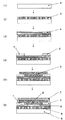
- FIG. 1 is a schematic view showing an embodiment of the field effect transistor of the present invention.
- FIG. 2 is a schematic view of a process for manufacturing one embodiment (bottom contact thin film transistor) of the field effect transistor of the present invention.
- FIG. 3 is a schematic view showing one embodiment of the organic EL element.
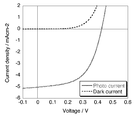
- FIG. 4 is a JV characteristic diagram of the organic solar battery element of Example 3.
- the present invention relates to a method for producing diantra [2,3-b: 2 ', 3'-f] thieno [3,2-b] thiophene.
- the present invention also relates to an organic electronic device obtained by forming a semiconductor layer using dianthra [2,3-b: 2 ′, 3′-f] thieno [3,2-b] thiophene as a semiconductor material.
- reaction formula of the present invention is as follows. Hereinafter, reaction formulas (1), (2), and (3) will be described in order.
- R 1 is preferably a methyl group, a trifluoromethyl group, a perfluorohexyl group, a 4-trifluoromethylphenyl group, or an aryl group in which all hydrogen atoms are replaced by fluorine atoms.
- pentafluorophenyl group, a trifluoromethyl SO 2 group, perfluorohexyl SO 2 group, 4-trifluoromethylphenyl SO 2 group, pentafluorophenyl SO 2 group is an aryl group in which all hydrogen atoms replaced with fluorine atoms Is mentioned.
- Preferable R 1 includes a methyl group and a trifluoromethyl SO 2 group. Many of these compounds (1) are also available as commercial products.
- reaction formula (1) will be described in detail.
- This reaction is a novel reaction, and it is converted to SMe by using dimethyldisulfide (Me 2 S 2 ) highly selectively at the 3-position of the compound (1) which is a starting material bonded to the oxygen atom at the 2-position. It is a feature.
- the inventors examined a base (alkyl metal reagent, alkyl earth metal reagent), a reaction solvent, a reaction temperature, and an operation procedure for metalation by hydrogen extraction at the 3-position, The inventors have found a production method in which SMe is converted to dimethyldisulfide with high selectivity at the 3-position of compound (1).
- an alkali metal reagent such as a lithium reagent, a sodium reagent, or a potassium reagent
- an alkyl earth metal reagent such as a magnesium reagent or a calcium reagent.
- methyl lithium, n-butyl lithium, t-butyl lithium, phenyl lithium, methyl magnesium chloride, butyl magnesium chloride, or the like can be used.
- Particularly preferred is the use of butyl lithium, which is a stable and strong base.
- the amount of the base used is desirably 0.5 mol or more and 10 mol or less with respect to 1 mol of the compound (1).
- the extraction of the hydrogen atom at the 3-position of compound (1) may be smooth.
- a basic compound may be added together with the alkyl metal reagent for the purpose of stabilizing the lithium reagent.
- Examples of basic compounds include N, N, N′-trimethylethylenediamine, dimethylamine, diisopropylamine, morpholine, and the like.
- the reaction temperature when reacting the compound (1) with a base is preferably in the range of ⁇ 100 ° C. to 30 ° C., more preferably ⁇ 30 ° C. to 10 ° C.
- any solvent can be used, but an ether solvent, an aliphatic solvent, or an aromatic solvent is desirable. In addition, it is desirable to use a solvent obtained by drying moisture.
- ether solvents used in the reaction include tetrahydrofuran (THF), diethyl ether, dimethoxyethane, dioxane and the like.
- aliphatic solvent examples include n-pentane, n-hexane, and n-heptane, and examples of the aromatic solvent include toluene and xylene.
- the amount of dimethyl disulfide used in the reaction is desirably 0.5 mol or more and 10 mol or less with respect to 1 mol of the compound (1).
- the purification method is not particularly limited, and a known purification method can be used according to the physical properties of the compound. Specifically, it can be purified by recrystallization, column chromatography or the like.
- R 2 represents an alkyl group.
- the alkyl group include straight-chain or branched-chain alkyl groups, and the carbon number thereof is 1 to 8, preferably 1 to 4, and more preferably 4.
- specific examples of the linear alkyl group include methyl, ethyl, n-propyl, n-butyl, n-pentyl, n-hexyl and the like.
- Specific examples of the branched chain alkyl group include C 3 -C 6 saturated branched chain alkyl groups such as i-propyl, i-butyl, t-butyl, i-pentyl, i-hexyl and the like.
- it is an n-butyl group that is easily available.
- the compound (compound (4)) produced by the reaction formula (2) is trans-1,2-bis (3-methylthioanthracen-2-yl) ethene.
- the reaction of the reaction formula (2) of the present invention is It is a novel reaction, and it reacts with the compound (3) together with elimination of the oxygen atom at the 2-position of the two-molecule compound (2) having a MeS group at the 3-position to produce the compound (4) with high selectivity. It is a feature.
- a Pd-based compound is used as a catalyst. However, Pd is easily violated by a sulfur compound and may lose its activity immediately.
- the present inventors have studied the catalyst, reaction solvent, reaction temperature, and operating procedure for effectively desorbing oxygen from the compound (2) and reacting with the compound (3) as described above.
- the present inventors have found a production method capable of obtaining compound (4) from 2) with high selectivity and high yield.
- R 1 of the compound (2) can be converted into a more optimal substituent and used as necessary when the reaction of the reaction formula (2) is performed.
- the mixing ratio of the compound (2) and the compound (3) when carrying out the reaction of the reaction formula (2) is that 1.8 mol to 2.5 mol of the compound (2) with respect to 1 mol of the compound (3). desirable. More preferably, it is carried out at 1.95 mol to 2.10 mol, and even more preferably at 1.95 mol to 2.05 mol.
- any Pd or Ni-based catalyst can be used, but at least one catalyst is tri-tert-butylphosphine, triadamantylphosphine, 1,3-bis ( 2,4,6-trimethylphenyl) imidazolidinium chloride, 1,3-bis (2,6-diisopropylphenyl) imidazolidinium chloride, 1,3-diadamantylimidazolidinium chloride, or a mixture thereof; metal Pd , Pd / C (with or without water), bis (triphenylphosphino) palladium dichloride (Pd (PPh 3 ) 2 Cl 2 ), palladium (II) acetate (Pd (OAc) 2 ), tetrakis (triphenylphosphine) palladium (Pd (PPh 3 ) 4 ), tetrakis (tripheny Ruphosphine) Nickel (Ni (PPh 3 ) 4 ), Nickel
- the amount of catalyst used is desirably 0.001 mol to 0.5 mol with respect to 1 mol of compound (2). You may add a catalyst in the range of the said usage-amount to the reaction solution which added the compound (2), the compound (3), and the catalyst. By adding the catalyst in two or more stages in this way, a reduction in the reaction rate due to catalyst deactivation may be suppressed.
- the reaction temperature for reacting compound (2) with compound (3) is usually from ⁇ 10 ° C. to 200 ° C. More preferably, it is 40 ° C to 180 ° C, and still more preferably 80 ° C to 150 ° C.
- a solvent may or may not be used. Any solvent can be used as long as it is a solvent used in ordinary organic synthesis.
- aromatic compounds such as chlorobenzene, o-dichlorobenzene, bromobenzene, nitrobenzene, toluene, xylene, and saturated aliphatic hydrocarbons such as n-hexane, n-heptane, n-pentane; cyclohexane, cycloheptane, cyclopentane
- Alicyclic hydrocarbons such as n-propyl bromide, n-butyl chloride, n-butyl bromide, dichloromethane, dibromomethane, dichloropropane, dibromopropane, dichloroethane, dibromoethane, dichloropropane, dibromopropane, dichlorobutane, chloroform, Saturated aliphatic halogen
- At least one high boiling point solvent having a boiling point of 100 ° C. or higher as the reaction solvent because the reaction rate is greatly improved and the selectivity of the reaction is further increased.
- High boiling point solvents having a boiling point of 100 ° C. or higher are amides (N-methyl-2-pyrrolidone (hereinafter referred to as NMP), N, N-dimethylformamide (hereinafter abbreviated as DMF), N, N-dimethylacetamide (hereinafter referred to as DMAc). )); Glycols (ethylene glycol, propylene glycol, polyethylene glycol); and sulfoxides (dimethyl sulfoxide (hereinafter abbreviated as DMSO)) are preferred, and N-methyl-2-pyrrolidone, N, N-dimethyl are more preferred.
- NMP N-methyl-2-pyrrolidone
- DMF N, N-dimethylformamide
- DMAc N-dimethylacetamide
- DMSO sulfoxides
- the purification method is not particularly limited, and a known purification method can be used according to the physical properties of the compound (4). Specifically, it can be purified by recrystallization, column chromatography or the like.
- the thin film of the present invention refers to a thin film formed from the dianthra [2,3-b: 2 ', 3'-f] thieno [3,2-b] thiophene of the present invention or a composition containing the same.
- the thickness of the thin film varies depending on the application, but is usually from 0.1 nm to 100 ⁇ m, preferably from 0.5 nm to 30 ⁇ m, more preferably from 1 nm to 20 ⁇ m.
- the thin film forming method of the present invention generally includes resistance heating evaporation, which is a vacuum process, electron beam evaporation, sputtering, molecular lamination, etc., and spin coating, drop casting, dip coating, and spraying, which are solution processes.
- Letterpress printing methods such as printing, flexographic printing, resin letterpress printing, offset printing methods, dry offset printing methods, pad printing methods, lithographic printing methods such as lithographic printing methods, intaglio printing methods such as gravure printing methods, silk screen printing methods, Examples thereof include a stencil printing method such as a stencil printing method and a lithographic printing method, an ink jet printing method, a microcontact printing method, and a method in which a plurality of these methods are combined.
- a resistance heating vapor deposition method that is a vacuum process
- a spin coating method that is a solution process
- a dip coating method that is a dip coating method
- an ink jet method screen printing, letterpress printing, and the like
- the film forming method required in each organic electronic device is different, it will be described later in the section of each device.
- the organic electronic device of the present invention contains the above-mentioned dianthra [2,3-b: 2 ', 3'-f] thieno [3,2-b] thiophene as an electronic material for electronics use.
- Examples of the organic electronic device include a thin film transistor, an organic EL element, a liquid crystal display element, a photoelectric conversion element, and an organic semiconductor laser element. These will be described in detail.
- a thin film transistor has two electrodes (a source electrode and a drain electrode) in contact with a semiconductor, and a current flowing between the electrodes is controlled by a voltage applied to another electrode called a gate electrode.
- a thin film transistor element often has a structure in which a gate electrode is insulated by an insulating film (Metal-Insulator-Semiconductor: MIS structure).
- An insulating film using a metal oxide film is called a MOS structure.
- MOS structure Metal-Insulator-Semiconductor
- a gate electrode is formed through a Schottky barrier, that is, an MES structure, but in the case of a thin film transistor using an organic semiconductor material, an MIS structure is often used.
- FIG. 1 shows some embodiments of the thin film transistor (element) of the present invention.
- 1 is a source electrode
- 2 is a semiconductor layer
- 3 is a drain electrode
- 4 is an insulator layer
- 5 is a gate electrode
- 6 is a substrate.
- positioning of each layer and an electrode can be suitably selected according to the use of an element.
- a to D are called lateral transistors because a current flows in a direction parallel to the substrate.
- A is called a bottom contact structure, and B is called a top contact structure.
- C has a source and drain electrode and an insulator layer on a semiconductor and further has a gate electrode formed thereon, which is called a bottom gate structure.
- D has a structure called a top & bottom contact type transistor.
- E is a schematic diagram of a transistor having a vertical structure, that is, a static induction transistor (SIT).
- SIT static induction transistor
- a large amount of carriers can move at a time because the current flow spreads in a plane.
- the source electrode and the drain electrode are arranged vertically, the distance between the electrodes can be reduced, so that the response is fast. Therefore, it can be preferably applied to uses such as high-speed switching with a large current.
- a substrate is not described in E in FIG. 1, a substrate is usually provided outside the source and drain electrodes represented by 1 and 3 in E in FIG. 1.
- the substrate 6 needs to be able to hold each layer formed thereon without peeling off.
- insulating materials such as resin plates, films, paper, glass, quartz, ceramics, etc .; those in which an insulating layer is formed on a conductive substrate such as metal or alloy by coating; materials consisting of various combinations such as resin and inorganic materials
- the resin film that can be used include polyethylene terephthalate, polyethylene naphthalate, polyethersulfone, polyamide, polyimide, polycarbonate, cellulose triacetate, and polyetherimide.
- the element can have flexibility, is flexible and lightweight, and improves practicality.
- the thickness of the substrate is usually 1 ⁇ m to 10 mm, preferably 5 ⁇ m to 5 mm.
- a conductive material is used for the source electrode 1, the drain electrode 3, and the gate electrode 5.
- the conductive polymer compound or the semiconductor may be doped.
- the dopant examples include inorganic acids such as hydrochloric acid and sulfuric acid; organic acids having an acidic functional group such as sulfonic acid; Lewis acids such as PF 5 , AsF 5 and FeCl 3 ; halogen atoms such as iodine; lithium, Metal atoms such as sodium and potassium; and the like. Boron, phosphorus, arsenic and the like are also frequently used as dopants for inorganic semiconductors such as silicon. In addition, a conductive composite material in which carbon black, metal particles, or the like is dispersed in the above dopant is also used.
- the distance (channel length) between the source and drain electrodes is an important factor that determines the characteristics of the device.
- the channel length is usually 0.1 to 300 ⁇ m, preferably 0.5 to 100 ⁇ m. If the channel length is short, the amount of current that can be extracted increases. However, since a leak current or the like occurs, an appropriate channel length is required.
- the width (channel width) between the source and drain electrodes is usually 10 to 10,000 ⁇ m, preferably 100 to 5000 ⁇ m. Further, this channel width can be made longer by forming the electrode structure into a comb structure, etc., and may be set to an appropriate length depending on the required amount of current or the structure of the element. . Each structure (shape) of the source and drain electrodes will be described.
- the structure of the source and drain electrodes may be the same or different.
- the length of the electrode may be the same as the channel width. There is no particular limitation on the width of the electrode, but a shorter one is preferable in order to reduce the area of the element as long as the electrical characteristics can be stabilized.
- the width of the electrode is usually 0.1 to 1000 ⁇ m, preferably 0.5 to 100 ⁇ m.
- the thickness of the electrode is usually 0.1 to 1000 nm, preferably 1 to 500 nm, more preferably 5 to 200 nm.
- a wiring is connected to each of the electrodes 1, 3, and 5, but the wiring is also made of substantially the same material as the electrode.
- An insulating material is used for the insulator layer 4.
- polymers such as polyparaxylylene, polyacrylate, polymethyl methacrylate, polystyrene, polyvinylphenol, polyamide, polyimide, polycarbonate, polyester, polyvinyl alcohol, polyvinyl acetate, polyurethane, polysulfone, epoxy resin, phenol resin, fluorine resin And copolymers combining these; metal oxides such as silicon dioxide, aluminum oxide, titanium oxide, and tantalum oxide; ferroelectric metal oxides such as SrTiO 3 and BaTiO 3 ; nitrides such as silicon nitride and aluminum nitride; A sulfide; a dielectric such as fluoride; or a polymer in which particles of the dielectric are dispersed can be used.
- the film thickness of the insulator layer 4 varies depending on the material, but is usually 0.1 nm to 100 ⁇ m, preferably 0.5 nm to 50 ⁇ m
- the dianthra [2,3-b: 2 ', 3'-f] thieno [3,2-b] thiophene of the present invention or a composition containing the same is used as the material for the semiconductor layer 2.
- the semiconductor layer 2 is formed as a thin film using the above method.
- other organic semiconductor materials and various additives may be mixed as necessary.
- the semiconductor layer 2 may be composed of a plurality of layers.
- the above additives are usually added in the range of 0.01 to 10% by weight, preferably 0.05 to 5% by weight, more preferably 0.1 to 3% by weight, when the total amount of the organic semiconductor material is 1. It is good to do. This is not the case when the semiconductor composition is used as the organic semiconductor material. A plurality of layers may also be formed for the semiconductor layer, but a single layer structure is more preferable.
- the thickness of the semiconductor layer 2 is preferably as thin as possible without losing necessary functions. In the lateral thin film transistor as shown in FIGS. 1A, 1B, and 1D, the leakage current increases as the film thickness increases. Therefore, if the film thickness exceeds a predetermined value, the element characteristics do not depend on the film thickness.
- the film thickness of the semiconductor layer for exhibiting the necessary function is usually 1 nm to 10 ⁇ m, preferably 5 nm to 5 ⁇ m, more preferably 10 nm to 3 ⁇ m.
- other layers can be provided as necessary between the substrate layer and the insulating film layer, between the insulating film layer and the semiconductor layer, or on the outer surface of the element.
- a protective layer is formed directly on the organic semiconductor layer or via another layer, the influence of outside air such as humidity can be reduced, and the ON / OFF ratio of the element can be increased.
- the electrical characteristics can be stabilized.
- the material of the protective layer is not particularly limited.
- films made of various resins such as acrylic resin such as epoxy resin and polymethyl methacrylate, polyurethane, polyimide, polyvinyl alcohol, fluororesin, polyolefin, etc .; silicon oxide, aluminum oxide, nitriding
- a film made of an inorganic oxide film such as silicon and a dielectric film such as a nitride film is preferably used, and a resin (polymer) having a low oxygen or moisture permeability and a low water absorption rate is particularly preferable.
- protective materials developed for organic EL displays can also be used.
- the film thickness of the protective layer can be selected according to the purpose, but is usually 100 nm to 1 mm.
- the film quality of the film formed thereon can be improved.
- the characteristics of organic semiconductor materials can vary greatly depending on the state of the film, such as molecular orientation.
- the surface treatment on the substrate or the like can control the molecular orientation at the interface between the substrate and the organic semiconductor layer to be formed thereafter, and can reduce the trap sites on the substrate and the insulator layer. Therefore, it is considered that characteristics such as carrier mobility are improved.
- the trap site refers to a functional group such as a hydroxyl group present in an untreated substrate.
- a functional group such as a hydroxyl group present in an untreated substrate.
- electrons are attracted to the functional group, and as a result, carrier mobility is lowered. Therefore, reducing trap sites is often effective for improving characteristics such as carrier mobility.
- Examples of the substrate treatment for improving the characteristics as described above include hydrophobization treatment with hexamethyldisilazane, cyclohexene, octyltrichlorosilane, octadecyltrichlorosilane, etc .; acid treatment with hydrochloric acid, sulfuric acid, acetic acid, etc .; sodium hydroxide, Alkaline treatment with potassium hydroxide, calcium hydroxide, ammonia, etc .; ozone treatment; fluorination treatment; plasma treatment with oxygen or argon; Langmuir / Blodgett film formation treatment; other insulator or semiconductor thin film formation treatment; Examples include mechanical treatment; electrical treatment such as corona discharge; and rubbing treatment using fibers and the like.
- a vacuum deposition method, a sputtering method, a coating method, a printing method, a sol-gel method, or the like can be appropriately employed as a method of providing each layer such as a substrate layer and an insulating film layer or an insulating film layer and an organic semiconductor layer. .
- the thin film transistor of the present invention is manufactured by providing various layers and electrodes necessary on the substrate 6 (see FIG. 2A).
- the substrate those described above can be used. It is also possible to perform the above-described surface treatment or the like on this substrate.
- the thickness of the substrate 6 is preferably thin as long as necessary functions are not hindered. Although it varies depending on the material, it is usually 1 ⁇ m to 10 mm, preferably 5 ⁇ m to 5 mm. Moreover, you may make it give the function of an electrode to a board
- a gate electrode 5 is formed on the substrate 6 (see FIG. 2B).
- the electrode material described above is used as the electrode material.
- various methods can be used. For example, a vacuum deposition method, a sputtering method, a coating method, a thermal transfer method, a printing method, a sol-gel method, and the like are employed. It is preferable to perform patterning as necessary so as to obtain a desired shape during or after film formation.
- Various methods can be used as the patterning method, and examples thereof include a photolithography method in which patterning and etching of a photoresist are combined.
- the film thickness of the gate electrode 5 varies depending on the material, but is usually 0.1 nm to 10 ⁇ m, preferably 0.5 nm to 5 ⁇ m, more preferably 1 nm to 3 ⁇ m. Moreover, when it serves as a gate electrode and a board
- An insulator layer 4 is formed over the gate electrode 5 (see FIG. 2 (3)).
- the insulator material those described above are used.
- Various methods can be used to form the insulator layer 4. For example, spin coating, spray coating, dip coating, casting, bar coating, blade coating and other coating methods, screen printing, offset printing, inkjet printing methods, vacuum deposition, molecular beam epitaxial growth, ion cluster beam method, ion plating Examples thereof include dry process methods such as a coating method, a sputtering method, an atmospheric pressure plasma method, and a CVD method.
- a sol-gel method alumite on aluminum, a method of forming an oxide film on a metal such as silicon dioxide on silicon, and the like are employed.
- molecules constituting the semiconductor at the interface between the two layers for example, dianthra [2,3-b: 2 ′, 3′-f] thieno [3,2] of the present invention.
- the insulator layer may be subjected to a predetermined surface treatment.
- the surface treatment method the same surface treatment as that of the substrate can be used.
- the thickness of the insulator layer 4 is preferably as thin as possible without impairing its function. Usually, the thickness is 0.1 nm to 100 ⁇ m, preferably 0.5 nm to 50 ⁇ m, more preferably 5 nm to 10 ⁇ m.
- the source electrode 1 and the drain electrode 3 can be formed in accordance with the case of the gate electrode 5 (see FIG. 2 (4)).
- Various additives can be used to reduce the contact resistance with the organic semiconductor layer.
- the organic semiconductor material As described above, the diantra [2,3-b: 2 ′, 3′-f] thieno [3,2-b] thiophene or a composition thereof is used as the organic semiconductor material.
- various methods can be used. Formation method in a vacuum process such as sputtering method, CVD method, molecular beam epitaxial growth method, vacuum deposition method; coating method such as dip coating method, die coater method, roll coater method, bar coater method, spin coating method, ink jet method, It is roughly classified into solution forming methods such as screen printing, offset printing, and microcontact printing.
- an organic thin film to be a semiconductor layer using the dianthra [2,3-b: 2 ′, 3′-f] thieno [3,2-b] thiophene of the present invention as a semiconductor material
- a method of forming an organic thin film formed by a vacuum process as a semiconductor layer is preferable, and a vacuum evaporation method is more preferable. It is possible to form a film by a solution process, and it is possible to adopt a printing method at a low cost.
- a method for obtaining an organic semiconductor layer by depositing an organic semiconductor material by a vacuum process will be described.
- a vapor deposition method is preferably employed.
- the degree of vacuum is usually 1.0 ⁇ 10 ⁇ 1 Pa or less, preferably 1.0 ⁇ 10 ⁇ 3 Pa or less.
- the characteristics of the organic semiconductor film and thus the thin film transistor may change depending on the substrate temperature during vapor deposition, it is preferable to select the substrate temperature carefully.
- the substrate temperature during vapor deposition is usually 0 to 200 ° C., preferably 10 to 150 ° C., more preferably 15 to 120 ° C., and further preferably 25 to 100 ° C.
- the deposition rate is usually 0.001 to 10 nm / second, preferably 0.01 to 1 nm / second.
- the film thickness of the organic semiconductor layer formed from the organic semiconductor material is usually 1 nm to 10 ⁇ m, preferably 5 nm to 5 ⁇ m, more preferably 10 nm to 3 ⁇ m.
- accelerated ions such as argon collide with the material target to knock out the material atoms and adhere to the substrate.
- a sputtering method may be used.
- the dianthra [2,3-b: 2 ′, 3′-f] thieno [3,2-b] thiophene of the present invention is dissolved or dispersed in a solvent or the like, and if necessary, other low molecular compounds or polymers.
- a composition containing additives such as a compound, a dopant, a dispersant, a surfactant, a leveling agent, and a surface tension adjusting agent is prepared as an ink for producing a semiconductor device, and the substrate (insulator layer, source electrode and drain electrode exposed) Part).
- Coating methods include casting, spin coating, dip coating, blade coating, wire bar coating, spray coating, and other coating methods, inkjet printing, screen printing, offset printing, letterpress printing, and other micro contact printing methods.
- the method of soft lithography, etc., or a method combining a plurality of these methods may be employed.
- a Langmuir project method in which a monomolecular film of an organic semiconductor layer produced by dropping the above ink on a water surface is transferred to a substrate and laminated, and two materials of liquid crystal or a melt state are used. It is also possible to adopt a method of sandwiching between substrates or introducing between substrates by capillary action.
- the environment such as the temperature of the substrate and the composition at the time of film formation is also important, and the characteristics of the transistor may change depending on the temperature of the substrate and the composition.
- the substrate temperature at the time of vapor deposition is usually 0 to 200 ° C., preferably 10 to 120 ° C., more preferably 15 to 100 ° C. Special care must be taken because it depends greatly on the solvent in the composition to be used.
- the film thickness of the organic semiconductor layer produced by this method is preferably thinner as long as the function is not impaired. There is a concern that the leakage current increases as the film thickness increases.
- the film thickness of the organic semiconductor layer is usually 1 nm to 10 ⁇ m, preferably 5 nm to 5 ⁇ m, more preferably 10 nm to 3 ⁇ m.
- the characteristics of the organic semiconductor layer thus formed can be further improved by post-processing.
- heat treatment reduces strain in the film generated during film formation, reduces pinholes, etc., and can control the arrangement and orientation in the film.
- the semiconductor characteristics can be improved and stabilized.
- this heat treatment is effective for improving the characteristics.
- This heat treatment is performed by heating the substrate after forming the organic semiconductor layer.
- the temperature of the heat treatment is not particularly limited, but is usually room temperature to 150 ° C., preferably 40 to 120 ° C., more preferably 45 to 100 ° C.
- the heat treatment time at this time is not particularly limited, but is usually about 1 minute to 24 hours, preferably about 2 minutes to 3 hours.
- the atmosphere at that time may be air, but may be an inert atmosphere such as nitrogen or argon.
- an oxidizing or reducing gas such as oxygen or hydrogen or an oxidizing or reducing liquid. You can also. This is often used for the purpose of increasing or decreasing the carrier density in the film, for example.
- characteristics of the organic semiconductor layer can be changed by adding a trace amount of elements, atomic groups, molecules, and polymers to the organic semiconductor layer.
- elements, atomic groups, molecules, and polymers For example, oxygen, hydrogen, hydrochloric acid, sulfuric acid, sulfonic acid and other acids; PF 5 , AsF 5 , FeCl 3 and other Lewis acids; iodine and other halogen atoms; sodium and potassium and other metal atoms; various organic semiconductor materials and the like can do. This can be achieved by bringing these gases into contact with the organic semiconductor layer, immersing them in a solution, or performing an electrochemical doping treatment.
- dopings may be added during the synthesis of the organic semiconductor compound, even after the organic semiconductor layer is not prepared, or may be added to the ink in the process of preparing the organic semiconductor layer using the ink for preparing the organic semiconductor element. It can be added in the process step of forming a thin film.
- a doping material is added to the material that forms the organic semiconductor layer during vapor deposition and co-evaporation is performed, or the organic semiconductor layer is mixed with the surrounding atmosphere when the organic semiconductor layer is formed (in the environment where the doping material is present, the organic semiconductor It is also possible to perform doping by accelerating ions in a vacuum and colliding with the film.
- doping effects include changes in electrical conductivity due to increase or decrease in carrier density, changes in carrier polarity (P-type and N-type), changes in Fermi level, and the like. Such doping is often used particularly in semiconductor elements using inorganic materials such as silicon.
- the protective layer 7 When the protective layer 7 is formed on the organic semiconductor layer, there is an advantage that the influence of outside air can be minimized and the electrical characteristics of the organic thin film transistor can be stabilized (see FIG. 2 (6)).
- the materials described above are used as the material for the protective layer.
- the protective layer 7 may have any thickness depending on the purpose, but is usually 100 nm to 1 mm.
- Various methods can be employed to form the protective layer.
- the protective layer is made of a resin, for example, a method of applying a resin solution and then drying to form a resin film; applying or vapor-depositing a resin monomer And then a method of polymerizing. Cross-linking treatment may be performed after film formation.
- the protective layer is made of an inorganic material, for example, a formation method in a vacuum process such as a sputtering method or a vapor deposition method, or a formation method in a solution process such as a sol-gel method can be used.
- a protective layer can be provided between the layers in addition to the organic semiconductor layer as necessary. These layers may help stabilize the electrical characteristics of the thin film transistor.
- dianthra [2,3-b: 2 ′, 3′-f] thieno [3,2-b] thiophene is used as an organic semiconductor material, it can be manufactured in a relatively low temperature process. is there. Therefore, flexible materials such as plastic plates and plastic films that could not be used under conditions exposed to high temperatures can also be used as the substrate. As a result, it is possible to manufacture a light, flexible, and hard-to-break element, which can be used as a switching element for an active matrix of a display.
- the thin film transistor of the present invention can also be used as a digital element and an analog element such as a memory circuit element, a signal driver circuit element, and a signal processing circuit element. Further, by combining these, it is possible to produce an IC card or an IC tag. Furthermore, since the thin film transistor of the present invention can change its characteristics by an external stimulus such as a chemical substance, it can be used as an FET sensor.
- Organic EL elements are attracting attention and can be used for applications such as solid, self-luminous large-area color display and illumination, and many developments have been made.
- the structure has a structure having two layers of a light emitting layer and a charge transport layer between a counter electrode composed of a cathode and an anode; an electron transport layer, a light emitting layer and a hole transport layer stacked between the counter electrodes.
- Known are those having a structure having three layers; and those having three or more layers; and those having a single light-emitting layer.
- the hole transport layer has a function of injecting holes from the anode, transporting holes to the light emitting layer, facilitating injection of holes into the light emitting layer, and a function of blocking electrons.
- the electron transport layer has a function of injecting electrons from the cathode, transporting electrons to the light emitting layer, facilitating injection of electrons into the light emitting layer, and blocking holes. Further, in the light emitting layer, excitons are generated by recombination of the injected electrons and holes, and the energy emitted in the process of radiative deactivation of the excitons is detected as light emission. Preferred embodiments of the organic EL device of the present invention are described below.
- the organic EL device of the present invention is a device that emits light by electrical energy, in which one or more organic thin films are formed between an anode and a cathode.
- the anode that can be used in the organic EL device of the present invention is an electrode having a function of injecting holes into a hole injection layer, a hole transport layer, and a light emitting layer.
- metal oxides, metals, alloys, conductive materials, and the like having a work function of 4.5 eV or more are suitable.
- conductive metal oxides such as tin oxide (NESA), indium oxide, indium tin oxide (ITO), indium zinc oxide (IZO), gold, silver, platinum, chromium And metals such as aluminum, iron, cobalt, nickel and tungsten, inorganic conductive materials such as copper iodide and copper sulfide, conductive polymers such as polythiophene, polypyrrole and polyaniline, and carbon.
- ITO or NESA it is preferable to use ITO or NESA.
- the anode may be made of a plurality of materials or may be composed of two or more layers.
- the resistance of the anode is not limited as long as it can supply a current sufficient for light emission of the element, but it is preferably low resistance from the viewpoint of power consumption of the element.
- an ITO substrate having a sheet resistance value of 300 ⁇ / ⁇ or less functions as an element electrode, but since it is possible to supply a substrate of several ⁇ / ⁇ , it is desirable to use a low-resistance product.
- the thickness of ITO can be arbitrarily selected according to the resistance value, but is usually 5 to 500 nm, preferably 10 to 300 nm. Examples of film forming methods such as ITO include a vapor deposition method, an electron beam method, a sputtering method, a chemical reaction method, and a coating method.
- the cathode that can be used in the organic EL device of the present invention is an electrode having a function of injecting electrons into an electron injection layer, an electron transport layer, and a light emitting layer.
- a metal or an alloy having a small work function (approximately 4 eV or less) is suitable.
- Specific examples include platinum, gold, silver, copper, iron, tin, zinc, aluminum, indium, chromium, lithium, sodium, potassium, calcium, and magnesium, but are not particularly limited. Lithium, sodium, potassium, calcium, and magnesium are preferable for increasing the electron injection efficiency and improving the device characteristics.
- an alloy with a metal such as aluminum or silver containing these low work function metals or an electrode having a structure in which these are laminated can be used.
- An inorganic salt such as lithium fluoride can be used for the electrode having a laminated structure.
- a transparent electrode that can be formed at a low temperature may be used. Examples of the film forming method include a vapor deposition method, an electron beam method, a sputtering method, a chemical reaction method, and a coating method, but are not particularly limited.
- the resistance of the cathode is not limited as long as it can supply a current sufficient for light emission of the element, but it is preferably low resistance from the viewpoint of power consumption of the element, and preferably about several hundred to several ⁇ / ⁇ .
- the film thickness is usually 5 to 500 nm, preferably 10 to 300 nm.
- oxides such as titanium oxide, silicon nitride, silicon oxide, silicon nitride oxide, germanium oxide, nitrides, or mixtures thereof, polyvinyl alcohol, vinyl chloride, hydrocarbon polymers, fluorine
- the cathode can be protected with a polymer, etc., and sealed with a dehydrating agent such as barium oxide, phosphorus pentoxide, or calcium oxide.
- the transparent substrate include a glass substrate and a polymer substrate.
- soda lime glass, non-alkali glass, quartz, or the like is used.
- the glass substrate may have a thickness sufficient to maintain mechanical and thermal strength, and a thickness of 0.5 mm or more is preferable.
- the material of the glass it is better that there are few ions eluted from the glass, and alkali-free glass is preferred.
- soda lime glass provided with a barrier coat such as SiO 2 is commercially available, it can also be used.
- the substrate made of a polymer other than glass include polycarbonate, polypropylene, polyethersulfone, polyethylene terephthalate, and an acrylic substrate.
- the organic thin film included in the organic EL element of the present invention is formed of one or more layers between the anode and cathode electrodes.
- the “layer” of one or more layers forming the organic thin film in the present invention is a hole transport layer, an electron transport layer, a hole transport light-emitting layer, an electron transport light-emitting layer, a hole block layer, an electron block
- a hole transport layer As shown in the layer, the hole injection layer, the electron injection layer, the light emitting layer, or the following structural example 9), it means a single layer having the functions of these layers.
- Examples of the configuration of the layer forming the organic thin film in the present invention include the following configuration examples 1) to 9), and any configuration may be used.
- the above 9) may be a single layer formed of a material generally called a bipolar light-emitting material; or only one layer including a light-emitting material and a hole transport material or an electron transport material.
- a material generally called a bipolar light-emitting material or only one layer including a light-emitting material and a hole transport material or an electron transport material.
- charges that is, holes and / or electrons can be efficiently transported and these charges can be recombined.
- the stability of the element can be prevented from being lowered and the light emission efficiency can be improved.
- the hole injection layer and the transport layer are formed by laminating a hole transport material alone or a mixture of two or more kinds of the materials.
- the hole transport material include N, N′-diphenyl-N, N′-di (3-methylphenyl) -4,4′-diphenyl-1,1′-diamine, N, N′-dinaphthyl-N, Triphenylamines such as N′-diphenyl-4,4′-diphenyl-1,1′-diamine, bis (N-allylcarbazole) or bis (N-alkylcarbazole) s, pyrazoline derivatives, stilbene compounds, hydrazones
- a polymer compound a triazole derivative, a heterocyclic compound typified by an oxadiazole derivative or a porphyrin derivative, or a polymer system, a polycarbonate, a styrene derivative, polyvinyl carbazole, polysilane, or
- the hole injection layer provided between the hole transport layer and the anode for improving the hole injection property includes phthalocyanine derivatives, starburst amines such as m-MTDATA, polythiophene such as PEDOT in the polymer system, polyvinyl Those prepared with carbazole derivatives and the like can be mentioned.
- the electron transport material As an electron transport material, it is necessary to efficiently transport electrons from the negative electrode between electrodes to which an electric field is applied.
- the electron transport material has high electron injection efficiency, and it is preferable to transport the injected electrons efficiently.
- the substance has a high electron affinity, a high electron mobility, excellent stability, and a substance that does not easily generate trapping impurities during manufacturing and use.
- quinolinol derivative metal complexes represented by tris (8-quinolinolato) aluminum complexes, tropolone metal complexes, perylene derivatives, perinone derivatives, naphthalimide derivatives, naphthalic acid derivatives, oxazole derivatives, oxadiazoles Derivatives, thiazole derivatives, thiadiazole derivatives, triazole derivatives, bisstyryl derivatives, pyrazine derivatives, phenanthroline derivatives, benzoxazole derivatives, quinoxaline derivatives, and the like are exemplified, but are not particularly limited.
- These electron transport materials are used alone, but may be laminated or mixed with different electron transport materials. Examples of the electron injection layer provided between the electron transport layer and the cathode for improving the electron injection property include metals such as cesium, lithium, and strontium, lithium fluoride, and the like.
- the hole blocking layer is formed by laminating and mixing hole blocking substances alone or two or more kinds.
- the hole blocking substance phenanthroline derivatives such as bathophenanthroline and bathocuproin, silole derivatives, quinolinol derivative metal complexes, oxadiazole derivatives and oxazole derivatives are preferable.
- the hole blocking substance is not particularly limited as long as it is a compound that can prevent holes from flowing out from the cathode side to the outside of the device and thereby reducing luminous efficiency.
- the light emitting layer means an organic thin film that emits light, and can be said to be, for example, a hole transporting layer, an electron transporting layer, or a bipolar transporting layer having strong light emitting properties.
- the light emitting layer only needs to be formed of a light emitting material (host material, dopant material, etc.), which may be a mixture of a host material and a dopant material or a host material alone. Each of the host material and the dopant material may be one kind or a combination of a plurality of materials.
- the dopant material may be included in the host material as a whole, or may be included partially.
- the dopant material may be either laminated or dispersed.
- Examples of the light emitting layer include the above-described hole transport layer and electron transport layer.
- Materials used for the light-emitting layer include carbazole derivatives, anthracene derivatives, naphthalene derivatives, phenanthrene derivatives, phenylbutadiene derivatives, styryl derivatives, pyrene derivatives, perylene derivatives, quinoline derivatives, tetracene derivatives, perylene derivatives, quinacridone derivatives, coumarin derivative porphyrins. Derivatives and phosphorescent metal complexes (Ir complex, Pt complex, Eu complex, etc.) can be mentioned.
- These thin film formation methods are generally vacuum heating processes such as resistance heating vapor deposition, electron beam vapor deposition, sputtering, molecular lamination method, solution processes such as casting, spin coating, dip coating, blade coating, wire bar coating, spraying.
- a coating method such as coating, a printing method such as ink jet printing, screen printing, offset printing, and relief printing, a soft lithography method such as a microcontact printing method, and a combination of these methods may be employed.
- the thickness of each layer depends on the resistance value and charge mobility of each substance and cannot be limited, but is selected from 0.5 to 5000 nm. The thickness is preferably 1 to 1000 nm, more preferably 5 to 500 nm.
- the diant [2 of the present invention is formed on one or a plurality of thin films such as a light emitting layer, a hole transport layer, and an electron transport layer, which are present between the anode and cathode electrodes.
- 3-b 2 ′, 3′-f] thieno [3,2-b] thiophene, an element that efficiently emits light even with low electric energy can be obtained.
- the organic EL device of the present invention comprises the dianthra [2,3-b: 2 ′, 3′-f] thieno [3,2-b] thiophene of the present invention in one or more layers between the anode and the cathode. It can be obtained by forming a layer.
- the dianthra [2,3-b: 2 ′, 3′-f] thieno [3,2-b] thiophene of the present invention is preferably used as a hole transport layer or a light emitting layer. It can. For example, it can be used in combination with the above-described electron transport material, hole transport material, light emitting material, or the like.
- quinolinol derivative metal complex represented by tris (8-quinolinolato) aluminum complex, tropolone metal complex, perylene derivative, perinone derivative, naphthalimide derivative, naphthalic acid derivative, bisstyryl derivative, pyrazine derivative, phenanthroline derivative, benzoxazole derivative Quinoxaline derivatives, triphenylamines, bis (N-allylcarbazole) or bis (N-alkylcarbazole) s, pyrazoline derivatives, stilbene compounds, hydrazone compounds, heterocyclic compounds represented by oxadiazole derivatives, etc. Although it is mentioned, it is not particularly limited. These can be used alone, but can also be used by laminating or mixing different materials.
- the dopant material when the dianthra [2,3-b: 2 ′, 3′-f] thieno [3,2-b] thiophene of the present invention is used as a host material in combination with a dopant material, bis ( Perylene derivatives such as diisopropylphenyl) perylenetetracarboxylic imide, perinone derivatives, 4- (dicyanomethylene) -2-methyl-6- (p-dimethylaminostyryl) -4H-pyran (DCM) and its analogs, magnesium phthalocyanine metal phthalocyanine derivatives such as aluminum chloro phthalocyanine, rhodamine compounds, Deazafurabin derivatives, coumarin derivatives, oxazine compounds, squarylium compounds, violanthrone compound, Nile red, pyrromethene derivatives such as 5-Shianopirometen -BF 4 complex, further phosphorescent material Eu complexes having
- the amount of dopant material used is usually used at 30% by mass or less based on the host material. Preferably it is 20 mass% or less, More preferably, it is 10 mass% or less.
- a method for doping the host material with the dopant material in the light emitting layer it can be formed by a co-evaporation method with the host material. It is also possible to use it sandwiched between host materials. In this case, you may laminate
- dopant layers can form each layer alone, or may be used by mixing them.
- the dopant material may be polyvinyl chloride, polycarbonate, polystyrene, polystyrene sulfonic acid, poly (N-vinylcarbazole), poly (methyl) (meth) acrylate, polybutyl methacrylate, polyester, polysulfone, as a polymer binder.
- Solvent-soluble resins such as polyphenylene oxide, polybutadiene, hydrocarbon resin, ketone resin, phenoxy resin, polysulfone, polyamide, ethyl cellulose, vinyl acetate, ABS resin, polyurethane resin, phenol resin, xylene resin, petroleum resin, urea resin, melamine resin
- a curable resin such as an unsaturated polyester resin, an alkyd resin, an epoxy resin, or a silicone resin.
- the method for forming a thin film used in the organic EL device according to the present invention is generally performed using the dianthra [2,3-b: 2 ′, 3′-f] thieno [3,2-b] thiophene or the composition of the present invention.
- vacuum heating processes such as resistance heating deposition, electron beam deposition, sputtering, molecular lamination, solution processes such as casting, spin coating, dip coating, blade coating, wire bar coating, spray coating, etc.
- inkjet Printing methods such as printing, screen printing, offset printing and letterpress printing, soft lithography methods such as microcontact printing methods, and a combination of these methods may be employed.
- Resistance heating vapor deposition, electron beam vapor deposition, sputtering, molecular lamination method, coating method by dissolving and dispersing in solvent or resin (spin coating, casting, dip coating, etc.), LB method, ink jet method, etc. are not particularly limited. .
- resistance heating vapor deposition is preferable in terms of characteristics.
- the thickness of each layer is not limited because it is set according to the resistance value of the light-emitting substance, but is selected from 0.5 to 5000 nm. The thickness is preferably 1 to 1000 nm, more preferably 5 to 500 nm.
- the organic EL element of the present invention can be suitably used as a flat panel display. It can also be used as a flat backlight. In this case, either a light emitting colored light or a light emitting white light can be used.
- the backlight is mainly used for the purpose of improving the visibility of a display device that does not emit light, and is used for a liquid crystal display device, a clock, an audio device, an automobile panel, a display board, a sign, and the like.
- the backlight using the light emitting element of the present invention is thin, The above problem is solved because of its light weight. Similarly, it can be usefully used for illumination.
- an organic solar cell element is the same as that of a silicon-based solar cell, in which a layer for generating power is sandwiched between an anode and a cathode, and holes and electrons generated by absorbing light are received by each electrode as a solar cell.
- the power generation layer is composed of a P-type donor material, an N-type acceptor material, and other materials such as a buffer layer, and an organic solar cell is used in which an organic material is used.
- the structures include Schottky junctions, heterojunctions, bulk heterojunctions, nanostructure junctions, hybrids, etc., but each material efficiently absorbs incident light and generates charges. It functions as a solar cell by separating, transporting and collecting electrons).
- the anode and cathode in the solar cell element of the present invention are the same as those of the organic EL element described above. Since it is necessary to take in light efficiently, it is desirable to use an electrode having transparency in the absorption wavelength region of the power generation layer. Moreover, in order to have a favorable solar cell characteristic, it is preferable that sheet resistance is 20 ohms / square or less.
- the power generation layer in the solar cell element of the present invention is a single layer forming an organic thin film containing at least the dianthra [2,3-b: 2 ′, 3′-f] thieno [3,2-b] thiophene of the present invention. Or it is formed of a plurality of layers. Although the structure shown above can be adopted, it is basically composed of a P-type donor material, an N-type acceptor material, and a buffer layer.
- P-type donor materials include compounds that can transport holes in the same manner as the hole injection and hole transport layers described in the section of organic EL elements, polyparaphenylene vinylene derivatives, polythiophene derivatives, and polyfluorene derivatives. ⁇ -conjugated polymers such as polyaniline derivatives, and polymers having carbazole and other heterocyclic side chains.
- Examples of the low molecular compound include pentacene derivatives, rubrene derivatives, porphyrin derivatives, phthalocyanine derivatives, indigo derivatives, quinacridone derivatives, merocyanine derivatives, cyanine derivatives, squalium derivatives, benzoquinone derivatives, and the like.
- the N-type acceptor layer basically has a compound capable of transporting electrons, such as the electron transport layer described in the section of the organic EL element, an oligomer or polymer having a skeleton of pyridine and its derivative, and a quinoline and its derivative as a skeleton.
- Polymers such as oligomers and polymers, polymers having benzophenanthrolines and derivatives thereof, cyanopolyphenylene vinylene derivatives (CN-PPV, etc.), fluorinated phthalocyanine derivatives, perylene derivatives, naphthalene derivatives, bathocuproine derivatives, C60 and C70
- low molecular weight materials such as fullerene derivatives such as PCBM. Each of them preferably absorbs light efficiently and generates a charge, and the material used has a high extinction coefficient.
- the dianthra [2,3-b: 2 ', 3'-f] thieno [3,2-b] thiophene of the present invention can be particularly suitably used as a P-type donor material.
- the method for forming the thin film for the power generation layer of the organic solar cell of the present invention may be the same as the method described in the above-mentioned section of the organic EL element.
- the thickness of the thin film varies depending on the configuration of the solar cell, it is better to thicken it in order to absorb light sufficiently and prevent short circuiting.
- the thinner is suitable.
- about 10 to 5000 nm is suitable for the power generation layer.
- the Devices include solid-state image sensors as image sensors, and charge coupled devices (CCD) that have the function of converting video signals such as moving images and still images into digital signals. It is also expected to be used as various sensors that take advantage of the flexible functionality inherent to organic matter.
- dianthra [2,3-b: 2 ′, 3′-f] thieno [3,2-b] thiophene of the present invention is a compound having organic semiconductor properties, it is expected to be used as an organic semiconductor laser device.
- a resonator structure is incorporated in an organic semiconductor element containing diantra [2,3-b: 2 ′, 3′-f] thieno [3,2-b] thiophene of the present invention, and carriers are efficiently injected. If the density of the excited state can be sufficiently increased, it is expected that the light will be amplified and cause laser oscillation.
- diantra [2,3-b: 2 ', 3'-f] thieno [3,2-b] thiophene can be synthesized easily and efficiently.
- Example 2 Topic Contact Field Effect Transistor
- An n-doped silicon wafer with 300 nm SiO 2 thermal oxide film (surface resistance 0.02 ⁇ ⁇ cm or less) treated with octadecyltrichlorosilane was placed in a vacuum deposition apparatus, and the degree of vacuum in the apparatus was 3.0 ⁇ 10 ⁇ . It exhausted until it became 3 Pa or less.
- the dianthra [2,3-b: 2 ′, 3′-f] thieno [3,2-b] obtained in Example 1 was applied to this electrode under the condition of a substrate temperature of about 100 ° C. by resistance heating vapor deposition. Thiophene was deposited to a thickness of 25 nm to form a semiconductor layer (2).
- a shadow mask for electrode preparation is attached to this substrate, placed in a vacuum vapor deposition apparatus, evacuated until the degree of vacuum in the apparatus is 1.0 ⁇ 10 ⁇ 4 Pa or less, and gold electrode is formed by resistance heating vapor deposition That is, the source electrode (1) and the drain electrode (3) were vapor-deposited to a thickness of 40 nm to obtain a TC (top contact) type field effect transistor of the present invention.
- the thermal oxide film in the n-doped silicon wafer with the thermal oxide film has the function of the insulating layer (4), and the n-doped silicon wafer is the substrate (6) and the gate electrode (5).
- the obtained field effect transistor was installed in a prober, and semiconductor characteristics were measured using a semiconductor parameter analyzer 4155C (manufactured by Agilent). For semiconductor characteristics, the gate voltage was scanned from 10 V to -100 V in 20 V steps, the drain voltage was scanned from 10 V to -100 V, and the drain current-drain voltage was measured. As a result, current saturation was observed, and from the obtained voltage-current curve, the device showed a p-type semiconductor, and the carrier mobility was 2.5 to 3.0 cm 2 / Vs.
- Example 3 A glass substrate (manufactured by Tokyo Sanyo Vacuum Co., Ltd., 20 ⁇ / ⁇ or less) on which an ITO transparent conductive film was deposited to 115 nm was UV-ozone cleaned before device fabrication. This glass substrate was placed in a vacuum vapor deposition apparatus and evacuated until the degree of vacuum in the apparatus became 3.0 ⁇ 10 ⁇ 3 Pa or less. The dianthra [2,3-b: 2 ′, 3′-f] thieno [3,2-b] thiophene obtained in Example 1 was deposited on this electrode to a thickness of 40 nm by resistance heating evaporation. A semiconductor layer was formed.
- FIG. 4 shows a JV characteristic diagram of the organic solar cell element of this example.
- organic field effect transistors and organic thin-film solar cell elements were produced and their practicality was confirmed. Since dianthra [2,3-b: 2 ′, 3′-f] thieno [3,2-b] thiophene obtained simply and efficiently according to the present invention has excellent characteristic values, organic field effect transistors, It can be said that it is a very useful compound as a material for various organic electronic devices such as organic light emitting diodes, organic light emitting transistors, organic solar cells, organic lasers, and organic optical sensors.
Abstract
A dianthra[2,3-b:2',3'-f]thieno[3,2-b]thiophene is produced by subjecting a specific anthracene derivative to sulfur methylation, reacting the anthracene derivative with a specific tin compound, and then subjecting the reacted anthracene and tin compound to cyclization.
Description
本発明は、ジアントラ[2,3-b:2’,3’-f]チエノ[3,2-b]チオフェンの新規製造方法に関する。また、本発明は当該化合物を利用した、有機エレクトロニクスデバイスに関する。
The present invention relates to a novel process for producing diantra [2,3-b: 2 ', 3'-f] thieno [3,2-b] thiophene. The present invention also relates to an organic electronic device using the compound.
近年、有機エレクトロニクスデバイスへの関心が高まっている。その特徴としてはフレキシブルな構造をとり、大面積化が可能である事、更にはデバイス製造プロセスにおいて安価で高速の印刷方法を可能にすることが挙げられる。代表的なデバイスとしては有機光電変換素子、有機EL素子、有機トランジスタ素子などが挙げられる。有機光電変換素子としては、有機薄膜太陽電池、光センサー、イメージセンサーとしての研究開発がなされている。また、有機EL素子としては携帯電話のディスプレイからTVなどへ応用されており、有機トランジスタ素子としてはフレキシブルなディスプレイや安価なICへの研究開発がなされている。
In recent years, interest in organic electronics devices has increased. Its features include that it has a flexible structure and can have a large area, and further enables an inexpensive and high-speed printing method in the device manufacturing process. Typical devices include organic photoelectric conversion elements, organic EL elements, organic transistor elements, and the like. As an organic photoelectric conversion element, research and development as an organic thin film solar cell, an optical sensor, and an image sensor have been made. Also, organic EL elements are applied from mobile phone displays to TVs, and organic transistor elements are being researched and developed into flexible displays and inexpensive ICs.
これら有機エレクトロニクスデバイスの開発には、そのデバイスを構成する材料の開発が非常に重要である。そのため各分野において数多くの材料が検討されているが、十分な性能を有しているとは言えず、現在でも各種デバイスに有用な材料の開発が精力的に行われている。有機材料を用いることにより、高温での処理を必要としない低温プロセスでの製造が可能になり、用い得る基板材料の範囲が拡大される。その結果、フレキシブル且つ軽量で、壊れにくいデバイスの作製が実現可能となってきた。また各デバイスの作製工程において、半導体材料を溶解した溶液の塗布、インクジェットなどによる印刷等の手法が採用できる場合もあるため、大面積のデバイスを低コストで製造できる可能性がある。また有機の半導体材料用の化合物としては、様々なものが選択可能であり、その特性を活かしたこれまでに無い機能の発現が期待されている。
In developing these organic electronic devices, it is very important to develop materials that constitute the devices. For this reason, many materials have been studied in each field, but they cannot be said to have sufficient performance, and even now, materials that are useful for various devices are being actively developed. By using an organic material, it is possible to manufacture in a low temperature process that does not require high temperature processing, and the range of substrate materials that can be used is expanded. As a result, it has become possible to fabricate devices that are flexible, lightweight, and difficult to break. Further, in each device manufacturing process, there may be a case where a technique such as application of a solution in which a semiconductor material is dissolved, printing by ink jet, or the like may be employed, and thus a large area device may be manufactured at low cost. Various compounds for organic semiconductor materials can be selected, and an unprecedented function utilizing the characteristics is expected.
有機化合物を半導体材料として用いる例は、これまで各種の検討がなされており、例えばペンタセン、チオフェン又はこれらのオリゴマーやポリマーを利用したものが正孔輸送特性を有する材料としてすでに知られている(特許文献1及び特許文献2参照)。ペンタセンは5個のベンゼン環が直線状に縮合したアセン系の芳香族炭化水素であり、これを半導体材料として用いた電界効果トランジスタは、現在実用化されているアモルファスシリコンに匹敵する電荷の移動度(キャリア移動度)を示すことが報告されている。しかしペンタセンを用いた電界効果トランジスタは、環境による劣化が起こり、安定性に問題がある。またチオフェン系の化合物を用いた場合においても同様の問題点があり、いずれも実用性の高い材料とは言いがたいのが現状である。近年では、大気中において安定でかつ高いキャリア移動度を示すジナフト[2,3-b:2’,3’-f]チエノ[3,2-b]チオフェン(DNTT)などが開発され注目を浴びるようになってきた(特許文献3及び非特許文献1参照)。
Various studies have been made on examples in which an organic compound is used as a semiconductor material. For example, a material using pentacene, thiophene, or an oligomer or polymer thereof is already known as a material having a hole transport property (patents). Reference 1 and Patent Document 2). Pentacene is an acene-based aromatic hydrocarbon in which five benzene rings are linearly condensed. A field effect transistor using this as a semiconductor material has a charge mobility comparable to amorphous silicon currently in practical use. It has been reported to show (carrier mobility). However, a field effect transistor using pentacene is deteriorated due to the environment and has a problem in stability. In addition, when using thiophene compounds, there are similar problems, and it is difficult to say that all of them are highly practical materials. In recent years, dinaphtho [2,3-b: 2 ′, 3′-f] thieno [3,2-b] thiophene (DNTT), which exhibits stable and high carrier mobility in the atmosphere, has been developed and attracts attention. (See Patent Document 3 and Non-Patent Document 1).
しかし、これらの化合物でも有機ELなどのディスプレイのアプリケーションに用いるためには更に高いキャリア移動度が必要であり、また、太陽電池や光センサー等のアプリケーションに用いるためには、特定の波長に対する吸収がある等の特徴ある光電変換能が必要であり、マーケットからの強い要求がある。更に耐久性の観点からも高品質・高性能な有機半導体材料の開発が求められている。ジナフト[2,3-b:2’,3’-f]チエノ[3,2-b]チオフェン(DNTT)のπ系を拡張した化合物については特許文献3にジアントラ[2,3-b:2’,3’-f]チエノ[3,2-b]チオフェン(DATT)が記載されているが、その製造方法は工業的な製法であるとは言い難く、該化合物を産業上利用可能にせしめるためには、工業的に利用が可能な該化合物の製造方法の確立が必要であった。
However, even these compounds require higher carrier mobility in order to be used for display applications such as organic EL, and in order to be used in applications such as solar cells and optical sensors, they have absorption for specific wavelengths. Some characteristic photoelectric conversion ability is necessary, and there is a strong demand from the market. Furthermore, from the viewpoint of durability, development of high-quality and high-performance organic semiconductor materials is required. For a compound in which the π system of dinaphtho [2,3-b: 2 ′, 3′-f] thieno [3,2-b] thiophene (DNTT) is expanded, Patent Document 3 discloses dianthra [2,3-b: 2 Although ', 3'-f] thieno [3,2-b] thiophene (DATT) has been described, it is difficult to say that its production method is an industrial production method, and makes this compound industrially usable. Therefore, it was necessary to establish a method for producing the compound that can be used industrially.
本発明は優れたキャリア移動度を示す実用的な半導体としての特性を有する、ジアントラ[2,3-b:2’,3’-f]チエノ[3,2-b]チオフェンの新規な製造方法及びその化合物により形成された半導体層を有する有機エレクトロニクスデバイスを提供することを目的とする。
The present invention relates to a novel method for producing diantra [2,3-b: 2 ′, 3′-f] thieno [3,2-b] thiophene having a characteristic as a practical semiconductor exhibiting excellent carrier mobility. And an organic electronic device having a semiconductor layer formed of the compound.
本発明者らは、上記課題を解決すべく鋭意検討の結果、ジアントラ[2,3-b:2’,3’-f]チエノ[3,2-b]チオフェンを簡便かつ効率的に合成することを可能とする新規製造方法の開発に成功した。また、該化合物は優れたキャリア移動度を示す実用的な半導体としての特性を有することを見出した。それによって、該化合物からなる半導体材料、並びに該化合物により形成された半導体層を有する有機エレクトロニクスデバイスを提供することが可能となり、本発明を完成させるに至った。
As a result of intensive studies to solve the above problems, the present inventors synthesize dianthra [2,3-b: 2 ′, 3′-f] thieno [3,2-b] thiophene simply and efficiently. We have succeeded in developing a new manufacturing method that makes this possible. Moreover, it discovered that this compound has the characteristic as a practical semiconductor which shows the outstanding carrier mobility. Accordingly, it is possible to provide a semiconductor material composed of the compound and an organic electronic device having a semiconductor layer formed of the compound, and the present invention has been completed.
即ち、本発明は、
[1] ジアントラ[2,3-b:2’,3’-f]チエノ[3,2-b]チオフェンを製造する方法であって、
式(1)で表される化合物と、ジメチルスルフィドとを反応させ、式(2)で表される化合物を得る工程;
式(2)で表される化合物と、式(3)で表わされるスズ化合物とを反応させて、式(4)で表される化合物を得る工程;及び
式(4)で表される化合物を環化させ、ジアントラ[2,3-b:2’,3’-f]チエノ[3,2-b]チオフェンを得る工程;
を含む、上記方法。


(式中、R1、R2は置換基を表し、Meはメチル基を表す。)
[2] [1]に記載の方法により得られたジアントラ[2,3-b:2’,3’-f]チエノ[3,2-b]チオフェンを含む有機半導体材料。
[3] [1]に記載の方法により得られたジアントラ[2,3-b:2’,3’-f]チエノ[3,2-b]チオフェンを含有する半導体デバイス作製用インク。
[4] [1]に記載の方法により得られたジアントラ[2,3-b:2’,3’-f]チエノ[3,2-b]チオフェンを含有する有機半導体薄膜。
[5] [4]に記載の有機半導体薄膜層を有する有機エレクトロニクスデバイス。
[6] 光電変換素子、有機EL素子、有機半導体レーザー素子、液晶表示素子又は薄膜トランジスタ素子である、[5]に記載の有機エレクトロニクスデバイス。
[7] 太陽電池である、[5]に記載の有機エレクトロニクスデバイス。
[8] 光センサーである、[5]に記載の有機エレクトロニクスデバイス。
[9] [1]に記載の方法により得られたジアントラ[2,3-b:2’,3’-f]チエノ[3,2-b]チオフェンからなる半導体層を基板上に形成する工程を含む[5]に記載の有機エレクトロニクスデバイスの製造方法。
[10] 半導体層が蒸着法により形成される[9]に記載の有機エレクトロニクスデバイスの製造方法。
[11] [3]に記載の半導体デバイス作製用インクを塗布することによって半導体層を形成する[9]に記載の有機エレクトロニクスデバイスの製造方法。
に関する。 That is, the present invention
[1] A method for producing diantra [2,3-b: 2 ′, 3′-f] thieno [3,2-b] thiophene,
A step of reacting a compound represented by the formula (1) with dimethyl sulfide to obtain a compound represented by the formula (2);
A step of reacting a compound represented by formula (2) with a tin compound represented by formula (3) to obtain a compound represented by formula (4); and a compound represented by formula (4) Cyclization to obtain diantra [2,3-b: 2 ′, 3′-f] thieno [3,2-b] thiophene;
Including the above method.
(In the formula, R 1 and R 2 represent a substituent, and Me represents a methyl group.)
[2] An organic semiconductor material containing diantra [2,3-b: 2 ′, 3′-f] thieno [3,2-b] thiophene obtained by the method according to [1].
[3] An ink for producing a semiconductor device containing dianthra [2,3-b: 2 ′, 3′-f] thieno [3,2-b] thiophene obtained by the method according to [1].
[4] An organic semiconductor thin film containing diantra [2,3-b: 2 ′, 3′-f] thieno [3,2-b] thiophene obtained by the method according to [1].
[5] An organic electronic device having the organic semiconductor thin film layer according to [4].
[6] The organic electronics device according to [5], which is a photoelectric conversion element, an organic EL element, an organic semiconductor laser element, a liquid crystal display element, or a thin film transistor element.
[7] The organic electronic device according to [5], which is a solar cell.
[8] The organic electronic device according to [5], which is an optical sensor.
[9] A step of forming a semiconductor layer made of dianthra [2,3-b: 2 ′, 3′-f] thieno [3,2-b] thiophene obtained by the method according to [1] on a substrate. [5] The manufacturing method of the organic electronics device as described in [5].
[10] The method for producing an organic electronic device according to [9], wherein the semiconductor layer is formed by a vapor deposition method.
[11] The method for producing an organic electronic device according to [9], wherein the semiconductor layer is formed by applying the semiconductor device manufacturing ink according to [3].
About.
[1] ジアントラ[2,3-b:2’,3’-f]チエノ[3,2-b]チオフェンを製造する方法であって、
式(1)で表される化合物と、ジメチルスルフィドとを反応させ、式(2)で表される化合物を得る工程;
式(2)で表される化合物と、式(3)で表わされるスズ化合物とを反応させて、式(4)で表される化合物を得る工程;及び
式(4)で表される化合物を環化させ、ジアントラ[2,3-b:2’,3’-f]チエノ[3,2-b]チオフェンを得る工程;
を含む、上記方法。
(式中、R1、R2は置換基を表し、Meはメチル基を表す。)
[2] [1]に記載の方法により得られたジアントラ[2,3-b:2’,3’-f]チエノ[3,2-b]チオフェンを含む有機半導体材料。
[3] [1]に記載の方法により得られたジアントラ[2,3-b:2’,3’-f]チエノ[3,2-b]チオフェンを含有する半導体デバイス作製用インク。
[4] [1]に記載の方法により得られたジアントラ[2,3-b:2’,3’-f]チエノ[3,2-b]チオフェンを含有する有機半導体薄膜。
[5] [4]に記載の有機半導体薄膜層を有する有機エレクトロニクスデバイス。
[6] 光電変換素子、有機EL素子、有機半導体レーザー素子、液晶表示素子又は薄膜トランジスタ素子である、[5]に記載の有機エレクトロニクスデバイス。
[7] 太陽電池である、[5]に記載の有機エレクトロニクスデバイス。
[8] 光センサーである、[5]に記載の有機エレクトロニクスデバイス。
[9] [1]に記載の方法により得られたジアントラ[2,3-b:2’,3’-f]チエノ[3,2-b]チオフェンからなる半導体層を基板上に形成する工程を含む[5]に記載の有機エレクトロニクスデバイスの製造方法。
[10] 半導体層が蒸着法により形成される[9]に記載の有機エレクトロニクスデバイスの製造方法。
[11] [3]に記載の半導体デバイス作製用インクを塗布することによって半導体層を形成する[9]に記載の有機エレクトロニクスデバイスの製造方法。
に関する。 That is, the present invention
[1] A method for producing diantra [2,3-b: 2 ′, 3′-f] thieno [3,2-b] thiophene,
A step of reacting a compound represented by the formula (1) with dimethyl sulfide to obtain a compound represented by the formula (2);
A step of reacting a compound represented by formula (2) with a tin compound represented by formula (3) to obtain a compound represented by formula (4); and a compound represented by formula (4) Cyclization to obtain diantra [2,3-b: 2 ′, 3′-f] thieno [3,2-b] thiophene;
Including the above method.
(In the formula, R 1 and R 2 represent a substituent, and Me represents a methyl group.)
[2] An organic semiconductor material containing diantra [2,3-b: 2 ′, 3′-f] thieno [3,2-b] thiophene obtained by the method according to [1].
[3] An ink for producing a semiconductor device containing dianthra [2,3-b: 2 ′, 3′-f] thieno [3,2-b] thiophene obtained by the method according to [1].
[4] An organic semiconductor thin film containing diantra [2,3-b: 2 ′, 3′-f] thieno [3,2-b] thiophene obtained by the method according to [1].
[5] An organic electronic device having the organic semiconductor thin film layer according to [4].
[6] The organic electronics device according to [5], which is a photoelectric conversion element, an organic EL element, an organic semiconductor laser element, a liquid crystal display element, or a thin film transistor element.
[7] The organic electronic device according to [5], which is a solar cell.
[8] The organic electronic device according to [5], which is an optical sensor.
[9] A step of forming a semiconductor layer made of dianthra [2,3-b: 2 ′, 3′-f] thieno [3,2-b] thiophene obtained by the method according to [1] on a substrate. [5] The manufacturing method of the organic electronics device as described in [5].
[10] The method for producing an organic electronic device according to [9], wherein the semiconductor layer is formed by a vapor deposition method.
[11] The method for producing an organic electronic device according to [9], wherein the semiconductor layer is formed by applying the semiconductor device manufacturing ink according to [3].
About.
本発明の製造方法は、ジアントラ[2,3-b:2’,3’-f]チエノ[3,2-b]チオフェンの中間体を高選択的に製造でき、ジアントラ[2,3-b:2’,3’-f]チエノ[3,2-b]チオフェンを収率よく得ることが出来る工業的に有用な製造方法である。また、該製法で製造されたジアントラ[2,3-b:2’,3’-f]チエノ[3,2-b]チオフェンを有機エレクトロニクスデバイスに用いると、従来の有機半導体材料に比較して優れた性能を示す有機エレクトロニクスデバイスを提供することが出来る。
According to the production method of the present invention, an intermediate of dianthra [2,3-b: 2 ′, 3′-f] thieno [3,2-b] thiophene can be produced with high selectivity, and dianthra [2,3-b : 2 ′, 3′-f] thieno [3,2-b] thiophene is an industrially useful production method capable of obtaining a good yield. In addition, when dianthra [2,3-b: 2 ′, 3′-f] thieno [3,2-b] thiophene produced by the production method is used in an organic electronic device, it is compared with a conventional organic semiconductor material. An organic electronic device exhibiting excellent performance can be provided.
本発明を詳細に説明する。本発明は、ジアントラ[2,3-b:2’,3’-f]チエノ[3,2-b]チオフェンの製造方法に関する。また、半導体材料としてジアントラ[2,3-b:2’,3’-f]チエノ[3,2-b]チオフェンを使用し、半導体層を形成して得られる有機エレクトロニクスデバイスに関する。
The present invention will be described in detail. The present invention relates to a method for producing diantra [2,3-b: 2 ', 3'-f] thieno [3,2-b] thiophene. The present invention also relates to an organic electronic device obtained by forming a semiconductor layer using dianthra [2,3-b: 2 ′, 3′-f] thieno [3,2-b] thiophene as a semiconductor material.
以下、ジアントラ[2,3-b:2’,3’-f]チエノ[3,2-b]チオフェンの製造方法について詳細に述べる。本発明の製造方法によれば、当該化合物を非常に効率良く製造することができる。本発明の反応式は次の通りである。以下、反応式(1)、(2)、(3)を順に説明する。

Hereinafter, a method for producing diantra [2,3-b: 2 ′, 3′-f] thieno [3,2-b] thiophene will be described in detail. According to the production method of the present invention, the compound can be produced very efficiently. The reaction formula of the present invention is as follows. Hereinafter, reaction formulas (1), (2), and (3) will be described in order.
まず、ジアントラ[2,3-b:2’,3’-f]チエノ[3,2-b]チオフェンの製造における反応式(1)の出発物質である化合物(1)について説明する。
First, the compound (1) which is the starting material of the reaction formula (1) in the production of diantra [2,3-b: 2 ', 3'-f] thieno [3,2-b] thiophene will be described.
出発物質である化合物(1)において、R1として、好ましくはメチル基、トリフルオロメチル基、パーフルオロヘキシル基、4-トリフルオロメチルフェニル基、全ての水素原子がフッ素原子に置き換わったアリール基であるペンタフルオロフェニル基、トリフルオロメチルSO2基、パーフルオロヘキシルSO2基、4-トリフルオロメチルフェニルSO2基、全ての水素原子がフッ素原子に置き換わったアリール基であるペンタフルオロフェニルSO2基が挙げられる。好ましいR1としては、メチル基、トリフルオロメチルSO2基が挙げられる。これらの化合物(1)は、市販品としても入手可能なものが多い。
In the starting compound (1), R 1 is preferably a methyl group, a trifluoromethyl group, a perfluorohexyl group, a 4-trifluoromethylphenyl group, or an aryl group in which all hydrogen atoms are replaced by fluorine atoms. there pentafluorophenyl group, a trifluoromethyl SO 2 group, perfluorohexyl SO 2 group, 4-trifluoromethylphenyl SO 2 group, pentafluorophenyl SO 2 group is an aryl group in which all hydrogen atoms replaced with fluorine atoms Is mentioned. Preferable R 1 includes a methyl group and a trifluoromethyl SO 2 group. Many of these compounds (1) are also available as commercial products.
次に反応式(1)について詳細に説明する。この反応は新規な反応であり、2位の位置で酸素原子と結合している出発物質である化合物(1)の3位に高選択的にジメチルジスルフィド(Me2S2)を用いてSMe化するのが特徴である。この反応の開発のために、発明者らは、3位の水素引き抜きによるメタル化を行うための塩基(アルキル金属試薬、アルキル土類金属試薬)、反応溶媒、反応温度、操作手順を検討し、化合物(1)の3位に高選択的にジメチルジスルフィドを用いてSMe化する製造方法を見出したのである。
Next, reaction formula (1) will be described in detail. This reaction is a novel reaction, and it is converted to SMe by using dimethyldisulfide (Me 2 S 2 ) highly selectively at the 3-position of the compound (1) which is a starting material bonded to the oxygen atom at the 2-position. It is a feature. In order to develop this reaction, the inventors examined a base (alkyl metal reagent, alkyl earth metal reagent), a reaction solvent, a reaction temperature, and an operation procedure for metalation by hydrogen extraction at the 3-position, The inventors have found a production method in which SMe is converted to dimethyldisulfide with high selectivity at the 3-position of compound (1).

反応に使用する塩基としては、アルカリ金属試薬である、リチウム試薬、ナトリウム試薬、カリウム試薬;アルキル土類金属試薬である、マグネシウム試薬、カルシウム試薬の使用が望ましい。具体的には、メチルリチウム、n-ブチルリチウム、t-ブチルリチウム、フェニルリチウム、メチルマグネシウムクロリド、ブチルマグネシウムクロリドなどを用いることができる。特に好ましくは、安定で強力な塩基であるブチルリチウムの使用が望ましい。
As the base used for the reaction, it is desirable to use an alkali metal reagent, such as a lithium reagent, a sodium reagent, or a potassium reagent; an alkyl earth metal reagent, such as a magnesium reagent or a calcium reagent. Specifically, methyl lithium, n-butyl lithium, t-butyl lithium, phenyl lithium, methyl magnesium chloride, butyl magnesium chloride, or the like can be used. Particularly preferred is the use of butyl lithium, which is a stable and strong base.
塩基の使用量は、1molの化合物(1)に対し、0.5mol以上10mol以下であることが望ましい。塩基に化合物(1)を添加した反応溶液に、さらに上記使用量の範囲で塩基を添加してもよい。このように塩基を2段階で加えることにより、化合物(1)の3位の水素原子の引き抜きがスムーズになる場合がある。
The amount of the base used is desirably 0.5 mol or more and 10 mol or less with respect to 1 mol of the compound (1). You may add a base in the range of the said usage-amount to the reaction solution which added the compound (1) to the base. Thus, by adding a base in two steps, the extraction of the hydrogen atom at the 3-position of compound (1) may be smooth.
また、本実施の形態に係る化合物の製造方法においては、アルキル金属試薬とともに、リチウム試薬の安定化などを目的として、塩基性化合物(添加剤)を添加してもよい。塩基性化合物として、N、N,N’-トリメチルエチレンジアミン、ジメチルアミン、ジイソプロピルアミン、モルフォリンなどを挙げることができる。
Further, in the method for producing a compound according to the present embodiment, a basic compound (additive) may be added together with the alkyl metal reagent for the purpose of stabilizing the lithium reagent. Examples of basic compounds include N, N, N′-trimethylethylenediamine, dimethylamine, diisopropylamine, morpholine, and the like.
反応に際して、窒素置換下、乾燥窒素気流下で行うのが、望ましい。
It is desirable to carry out the reaction under nitrogen substitution and in a dry nitrogen stream.
上記化合物(1)と塩基とを反応させる時の反応温度としては、-100℃~30℃の範囲が好ましく、-30℃~10℃がより好ましい。
The reaction temperature when reacting the compound (1) with a base is preferably in the range of −100 ° C. to 30 ° C., more preferably −30 ° C. to 10 ° C.
この反応に際して、溶媒はいかなるものでも使用できるが、エーテル系の溶媒、脂肪族系の溶媒、又は芳香族系の溶媒が望ましい。また、これらの溶媒は水分を乾燥した溶媒を使用することが望ましい。
In this reaction, any solvent can be used, but an ether solvent, an aliphatic solvent, or an aromatic solvent is desirable. In addition, it is desirable to use a solvent obtained by drying moisture.
反応に用いるエーテル系溶媒としては、テトラヒドロフラン(THF)、ジエチルエーテル、ジメトキシエタン、ジオキサンなどが挙げられる。脂肪族系の溶媒としてはn-ペンタン、n-ヘキサン、n-ヘプタンなど、芳香族系の溶媒としては、トルエン、キシレンなどが挙げられる。
Examples of ether solvents used in the reaction include tetrahydrofuran (THF), diethyl ether, dimethoxyethane, dioxane and the like. Examples of the aliphatic solvent include n-pentane, n-hexane, and n-heptane, and examples of the aromatic solvent include toluene and xylene.
反応に用いるジメチルジスルフィドの使用量は、1molの化合物(1)に対し、0.5mol以上10mol以下であることが望ましい。
The amount of dimethyl disulfide used in the reaction is desirably 0.5 mol or more and 10 mol or less with respect to 1 mol of the compound (1).
上記で得られた、化合物(2)を精製する際、精製方法は特に限定されるものではなく、化合物の物性に応じて、公知の精製方法を用いることができる。具体的には再結晶、カラムクロマトグラフィー、などによって精製することができる。
When purifying the compound (2) obtained above, the purification method is not particularly limited, and a known purification method can be used according to the physical properties of the compound. Specifically, it can be purified by recrystallization, column chromatography or the like.
続いて反応式(2)における、化合物(2)と反応させる化合物(3)について説明する
Subsequently, the compound (3) to be reacted with the compound (2) in the reaction formula (2) will be described.

スズ化合物である式(3)において、R2は、アルキル基を表す。アルキル基としては直鎖又は分岐鎖のアルキル基が挙げられ、その炭素数は1~8であり、好ましくは1~4であり、より好ましくは4である。ここで、直鎖アルキル基の具体例としては、メチル、エチル、n-プロピル、n-ブチル、n-ペンチル、n-ヘキシル等が挙げられる。分岐鎖アルキル基の具体例としては、i-プロピル、i-ブチル、t-ブチル、i-ペンチル、i-ヘキシル等のC3-C6の飽和分鎖アルキル基が挙げられる。好ましくは、入手が容易なn-ブチル基である。
In the formula (3) is a tin compound, R 2 represents an alkyl group. Examples of the alkyl group include straight-chain or branched-chain alkyl groups, and the carbon number thereof is 1 to 8, preferably 1 to 4, and more preferably 4. Here, specific examples of the linear alkyl group include methyl, ethyl, n-propyl, n-butyl, n-pentyl, n-hexyl and the like. Specific examples of the branched chain alkyl group include C 3 -C 6 saturated branched chain alkyl groups such as i-propyl, i-butyl, t-butyl, i-pentyl, i-hexyl and the like. Preferably, it is an n-butyl group that is easily available.
以下に式(3)で示されるスズ化合物の具体例を示すが本発明はこれらに限定されるものではない。
Specific examples of the tin compound represented by the formula (3) are shown below, but the present invention is not limited thereto.


反応式(2)により生成した化合物(化合物(4))は、trans-1,2-ビス(3-メチルチオアントラセン-2-イル)エテンである。
The compound (compound (4)) produced by the reaction formula (2) is trans-1,2-bis (3-methylthioanthracen-2-yl) ethene.
特許文献3及び非特許文献1記載の従来の反応では、化合物(4)を合成するための原料のアルデヒド体の合成に非常に苦労していたが、本発明の反応式(2)の反応は新規な反応であり、MeS基を3位に有する2分子の化合物(2)の2位の酸素原子の脱離とともに化合物(3)と反応し、化合物(4)を高選択的製造するのが特徴である。一般的に、反応式(2)の反応は、触媒としてPd系の化合物が用いられるが、Pdは硫黄化合物に犯されやすく、すぐに活性を失うことがある。そのため、本発明者らは上記のように化合物(2)の酸素が効果的に脱離し、化合物(3)と反応する触媒、反応溶媒、反応温度、操作手順を検討し、2分子の化合物(2)から化合物(4)を高選択的・高収率で得ることができる製造方法を見出したのである。
In the conventional reactions described in Patent Document 3 and Non-Patent Document 1, although it has been very difficult to synthesize the aldehyde form as a raw material for synthesizing the compound (4), the reaction of the reaction formula (2) of the present invention is It is a novel reaction, and it reacts with the compound (3) together with elimination of the oxygen atom at the 2-position of the two-molecule compound (2) having a MeS group at the 3-position to produce the compound (4) with high selectivity. It is a feature. In general, in the reaction represented by the reaction formula (2), a Pd-based compound is used as a catalyst. However, Pd is easily violated by a sulfur compound and may lose its activity immediately. For this reason, the present inventors have studied the catalyst, reaction solvent, reaction temperature, and operating procedure for effectively desorbing oxygen from the compound (2) and reacting with the compound (3) as described above. The present inventors have found a production method capable of obtaining compound (4) from 2) with high selectivity and high yield.
ここで、化合物(2)のR1は反応式(2)の反応を行なう時に必要に応じて、より最適な置換基に変換して用いることができる。
Here, R 1 of the compound (2) can be converted into a more optimal substituent and used as necessary when the reaction of the reaction formula (2) is performed.
反応式(2)の反応を行なう際の化合物(2)と化合物(3)の混合比は、1molの化合物(3)に対し、化合物(2)を1.8mol~2.5molであるのが望ましい。1.95mol~2.10molで行うのがより好ましく、1.95mol~2.05molで行なうのがさらに好ましい。
The mixing ratio of the compound (2) and the compound (3) when carrying out the reaction of the reaction formula (2) is that 1.8 mol to 2.5 mol of the compound (2) with respect to 1 mol of the compound (3). desirable. More preferably, it is carried out at 1.95 mol to 2.10 mol, and even more preferably at 1.95 mol to 2.05 mol.
反応に使用する触媒としては、Pd又はNi系の触媒であればどんなものでも使用することが可能だが、少なくとも1つの触媒が、トリ-tert-ブチルホスフィン、トリアダマンチルホスフィン、1,3-ビス(2,4,6-トリメチルフェニル)イミダゾリジニウムクロライド、1,3-ビス(2,6-ジイソプロピルフェニル)イミダゾリジニウムクロライド、1,3-ジアダマンチルイミダゾリジニウムクロライド、又はそれらの混合物;金属Pd、Pd/C(含水又は非含水)、ビス(トリフェニルホスフィノ)パラジウムジクロライド(Pd(PPh3)2Cl2)、酢酸パラジウム(II)(Pd(OAc)2)、テトラキス(トリフェニルホスフィン)パラジウム(Pd(PPh3)4)、テトラキス(トリフェニルホスフィン) ニッケル(Ni(PPh3)4)、ニッケル(II)アセチルアセトネートNi(acac)2、ジクロロ(2,2’-ビピリジン)ニッケル、ジブロモビス(トリフェニルホスフィン)ニッケル(Ni(PPh3)2Br2)、ビス(ジフェニルホスフィノ)プロパンニッケルジクロライド(Ni((dppp)Cl2)、ビス(ジフェニルホスフィノ)エタンニッケルジクロライドNi(dppe)Cl2、又はそれらの混合物の群から選択されるリガンドを持つニッケル及びパラジウム触媒の群から選択される少なくとも1つの化合物を含んでいればよい。好ましい触媒として、Pd/C(含水又は非含水)、Pd(PPh3)2Cl2、Pd(PPh3)4が挙げられ、より好ましくは、Pd(PPh3)2Cl2、Pd(PPh3)4が挙げられる。
As the catalyst used in the reaction, any Pd or Ni-based catalyst can be used, but at least one catalyst is tri-tert-butylphosphine, triadamantylphosphine, 1,3-bis ( 2,4,6-trimethylphenyl) imidazolidinium chloride, 1,3-bis (2,6-diisopropylphenyl) imidazolidinium chloride, 1,3-diadamantylimidazolidinium chloride, or a mixture thereof; metal Pd , Pd / C (with or without water), bis (triphenylphosphino) palladium dichloride (Pd (PPh 3 ) 2 Cl 2 ), palladium (II) acetate (Pd (OAc) 2 ), tetrakis (triphenylphosphine) palladium (Pd (PPh 3 ) 4 ), tetrakis (tripheny Ruphosphine) Nickel (Ni (PPh 3 ) 4 ), Nickel (II) acetylacetonate Ni (acac) 2 , Dichloro (2,2′-bipyridine) nickel, Dibromobis (triphenylphosphine) nickel (Ni (PPh 3 ) 2 Br 2 ), bis (diphenylphosphino) propanenickel dichloride (Ni ((dppp) Cl 2 ), bis (diphenylphosphino) ethanenickel dichloride Ni (dppe) Cl 2 , or mixtures thereof It may contain at least one compound selected from the group of nickel and palladium catalysts having a ligand, and preferred catalysts include Pd / C (hydrous or non-hydrous), Pd (PPh 3 ) 2 Cl 2 , Pd (PPh 3) 4, and more preferably include, Pd (PP 3) 2 Cl 2, Pd ( PPh 3) 4 and the like.
触媒の使用量は、1molの化合物(2)に対し、0.001mol以上0.5mol以下であることが望ましい。化合物(2)と化合物(3)と触媒とを添加した反応溶液に、さらに上記使用量の範囲で触媒を添加してもよい。このように触媒を2段階以上に分けて加えることにより、触媒の失活による反応率の低下が抑えられる場合がある。
The amount of catalyst used is desirably 0.001 mol to 0.5 mol with respect to 1 mol of compound (2). You may add a catalyst in the range of the said usage-amount to the reaction solution which added the compound (2), the compound (3), and the catalyst. By adding the catalyst in two or more stages in this way, a reduction in the reaction rate due to catalyst deactivation may be suppressed.
化合物(2)と化合物(3)とを反応させる時の反応温度としては、通常-10℃~200℃で行なう。より好ましくは、40℃~180℃、さらに好ましくは、80℃~150℃である。
The reaction temperature for reacting compound (2) with compound (3) is usually from −10 ° C. to 200 ° C. More preferably, it is 40 ° C to 180 ° C, and still more preferably 80 ° C to 150 ° C.
反応に際して、窒素置換下又はアルゴン置換下等の不活性な雰囲気下や乾燥窒素気流下などで行うのが望ましい。
It is desirable to carry out the reaction under an inert atmosphere such as nitrogen substitution or argon substitution, or under a dry nitrogen stream.
反応の際は、溶媒を使用しても使用しなくてもよい。通常の有機合成に用いられる溶媒であれば、いかなるものでも使用可能である。例えば、クロロベンゼン、o-ジクロロベンゼン、ブロモベンゼン、ニトロベンゼン、トルエン、キシレン等の芳香族化合物や、n-ヘキサン、n-ヘプタン、n-ペンタン等の飽和脂肪族炭化水素;シクロヘキサン、シクロヘプタン、シクロペンタン等の脂環式炭化水素、n-プロピルブロマイド、n-ブチルクロライド、n-ブチルブロマイド、ジクロロメタン、ジブロモメタン、ジクロロプロパン、ジブロモプロパン、ジクロロエタン、ジブロモエタン、ジクロロプロパン、ジブロモプロパン、ジクロロブタン、クロロホルム、ブロモホルム、四塩化炭素、四臭化炭素、トリクロロエタン、テトラクロロエタン、ペンタクロロエタン等の飽和脂肪族ハロゲン化炭化水素;クロロシクロヘキサン、クロロシクロペンタン、ブロモシクロペンタン等のハロゲン化環状炭化水素;酢酸エチル、酢酸プロピル、酢酸ブチル、プロピオン酸メチル、プロピオン酸エチル、プロピオン酸プロピル、プロピオン酸ブチル、酪酸メチル、酪酸エチル、酪酸プロピル、酪酸ブチル等のエステル;アセトン、メチルエチルケトン、メチルイソブチルケトン等のケトン;を挙げることが出来る。これらの溶媒は単独でも2種以上混合して使用してもよい。
In the reaction, a solvent may or may not be used. Any solvent can be used as long as it is a solvent used in ordinary organic synthesis. For example, aromatic compounds such as chlorobenzene, o-dichlorobenzene, bromobenzene, nitrobenzene, toluene, xylene, and saturated aliphatic hydrocarbons such as n-hexane, n-heptane, n-pentane; cyclohexane, cycloheptane, cyclopentane Alicyclic hydrocarbons such as n-propyl bromide, n-butyl chloride, n-butyl bromide, dichloromethane, dibromomethane, dichloropropane, dibromopropane, dichloroethane, dibromoethane, dichloropropane, dibromopropane, dichlorobutane, chloroform, Saturated aliphatic halogenated hydrocarbons such as bromoform, carbon tetrachloride, carbon tetrabromide, trichloroethane, tetrachloroethane, pentachloroethane; chlorocyclohexane, chlorocyclopentane, bromocyclope Halogenated cyclic hydrocarbons such as tan; esters such as ethyl acetate, propyl acetate, butyl acetate, methyl propionate, ethyl propionate, propyl propionate, butyl propionate, methyl butyrate, ethyl butyrate, propyl butyrate, butyl butyrate; acetone And ketones such as methyl ethyl ketone and methyl isobutyl ketone. These solvents may be used alone or in combination of two or more.
また、反応溶媒として、沸点100℃以上の高沸点溶媒の少なくとも一種を使用すると、大幅に反応速度が向上したり、反応の選択性がより増すので好ましい。
Also, it is preferable to use at least one high boiling point solvent having a boiling point of 100 ° C. or higher as the reaction solvent because the reaction rate is greatly improved and the selectivity of the reaction is further increased.
沸点100℃以上の高沸点溶媒とはアミド類(N-メチル-2-ピロリドン(以下、NMP)、N,N-ジメチルホルムアミド(以下、DMFと略記)、N,N-ジメチルアセトアミド(以下、DMAc));グリコール類(エチレングリコール、プロピレングリコール、ポリエチレングリコール);及びスルホキシド類(ジメチルスルホキシド(以下、DMSOと略記))が好ましく、より好ましくは、N-メチル-2-ピロリドン、N,N-ジメチルホルムアミド、N,N-ジメチルアセトアミドである。
High boiling point solvents having a boiling point of 100 ° C. or higher are amides (N-methyl-2-pyrrolidone (hereinafter referred to as NMP), N, N-dimethylformamide (hereinafter abbreviated as DMF), N, N-dimethylacetamide (hereinafter referred to as DMAc). )); Glycols (ethylene glycol, propylene glycol, polyethylene glycol); and sulfoxides (dimethyl sulfoxide (hereinafter abbreviated as DMSO)) are preferred, and N-methyl-2-pyrrolidone, N, N-dimethyl are more preferred. Formamide, N, N-dimethylacetamide.
得られた化合物(4)を精製する際、精製方法は特に限定されるものではなく、化合物(4)の物性に応じて、公知の精製方法を用いることができる。具体的には再結晶、カラムクロマトグラフィー、などによって精製することができる。
When purifying the obtained compound (4), the purification method is not particularly limited, and a known purification method can be used according to the physical properties of the compound (4). Specifically, it can be purified by recrystallization, column chromatography or the like.
その後、反応式(3)の反応により、化合物(4)から下記のジアントラ[2,3-b:2’,3’-f]チエノ[3,2-b]チオフェンが誘導される。

Thereafter, the following dianthra [2,3-b: 2 ′, 3′-f] thieno [3,2-b] thiophene is derived from the compound (4) by the reaction of the reaction formula (3).
本発明の薄膜とは、本発明のジアントラ[2,3-b:2’,3’-f]チエノ[3,2-b]チオフェン又はそれを含む組成物から形成された薄膜を言う。薄膜の膜厚は、その用途によって異なるが、通常0.1nm~100μmであり、好ましくは0.5nm~30μmであり、より好ましくは1nm~20μmである。
The thin film of the present invention refers to a thin film formed from the dianthra [2,3-b: 2 ', 3'-f] thieno [3,2-b] thiophene of the present invention or a composition containing the same. The thickness of the thin film varies depending on the application, but is usually from 0.1 nm to 100 μm, preferably from 0.5 nm to 30 μm, more preferably from 1 nm to 20 μm.
本発明の薄膜の形成方法は、一般的に、真空プロセスである抵抗加熱蒸着、電子ビーム蒸着、スパッタリング、分子積層法などや、溶液プロセスであるスピンコート法、ドロップキャスト法、ディップコート法、スプレー法、フレキソ印刷、樹脂凸版印刷などの凸版印刷法、オフセット印刷法、ドライオフセット印刷法、パッド印刷法、石版印刷法などの平板印刷法、グラビア印刷法などの凹版印刷法、シルクスクリーン印刷法、謄写版印刷法、リソグラフ印刷法などの孔版印刷法、インクジェット印刷法、マイクロコンタクトプリント法等、さらにはこれらの手法を複数組み合わせた方法が挙げられる。通常は、真空プロセスである抵抗加熱蒸着法や溶液プロセスであるスピンコート法、ディップコート法、インクジェット法、スクリーン印刷、凸版印刷などが好ましい。また、各有機エレクトロニクスデバイスにおいて必要な製膜方法も異なるため、各デバイスの項においても後述する。
The thin film forming method of the present invention generally includes resistance heating evaporation, which is a vacuum process, electron beam evaporation, sputtering, molecular lamination, etc., and spin coating, drop casting, dip coating, and spraying, which are solution processes. Letterpress printing methods such as printing, flexographic printing, resin letterpress printing, offset printing methods, dry offset printing methods, pad printing methods, lithographic printing methods such as lithographic printing methods, intaglio printing methods such as gravure printing methods, silk screen printing methods, Examples thereof include a stencil printing method such as a stencil printing method and a lithographic printing method, an ink jet printing method, a microcontact printing method, and a method in which a plurality of these methods are combined. Usually, a resistance heating vapor deposition method that is a vacuum process, a spin coating method that is a solution process, a dip coating method, an ink jet method, screen printing, letterpress printing, and the like are preferable. Moreover, since the film forming method required in each organic electronic device is different, it will be described later in the section of each device.
本発明の有機エレクトロニクスデバイスとは前記のジアントラ[2,3-b:2’,3’-f]チエノ[3,2-b]チオフェンをエレクトロニクス用途の電子材料として含有するものである。有機エレクトロニクスデバイスとして例えば薄膜トランジスタや有機EL素子、液晶表示素子、光電変換素子、有機半導体レーザー素子などが挙げられる。これらについて詳細に説明する。
The organic electronic device of the present invention contains the above-mentioned dianthra [2,3-b: 2 ', 3'-f] thieno [3,2-b] thiophene as an electronic material for electronics use. Examples of the organic electronic device include a thin film transistor, an organic EL element, a liquid crystal display element, a photoelectric conversion element, and an organic semiconductor laser element. These will be described in detail.
まず薄膜トランジスタについて詳しく説明する。
薄膜トランジスタは、半導体に接して2つの電極(ソース電極及びドレイン電極)があり、その電極間に流れる電流を、ゲート電極と呼ばれるもう一つの電極に印加する電圧で制御するものである。 First, the thin film transistor will be described in detail.
A thin film transistor has two electrodes (a source electrode and a drain electrode) in contact with a semiconductor, and a current flowing between the electrodes is controlled by a voltage applied to another electrode called a gate electrode.
一般に、薄膜トランジスタ素子はゲート電極が絶縁膜で絶縁されている構造(Metal-Insulator-Semiconductor;MIS構造)がよく用いられる。絶縁膜に金属酸化膜を用いるものはMOS構造と呼ばれる。他には、ショットキー障壁を介してゲート電極が形成されている構造、すなわちMES構造もあるが、有機半導体材料を用いた薄膜トランジスタの場合、MIS構造がよく用いられる。
Generally, a thin film transistor element often has a structure in which a gate electrode is insulated by an insulating film (Metal-Insulator-Semiconductor: MIS structure). An insulating film using a metal oxide film is called a MOS structure. In addition, there is a structure in which a gate electrode is formed through a Schottky barrier, that is, an MES structure, but in the case of a thin film transistor using an organic semiconductor material, an MIS structure is often used.
以下、図を用いて本発明による有機系の薄膜トランジスタについてより詳細に説明するが、本発明はこれらの構造には限定されない。
図1に、本発明の薄膜トランジスタ(素子)のいくつかの態様例を示す。各例において、1がソース電極、2が半導体層、3がドレイン電極、4が絶縁体層、5がゲート電極、6が基板を表す。尚、各層や電極の配置は、素子の用途により適宜選択できる。A~Dは基板と並行方向に電流が流れるので、横型トランジスタと呼ばれる。Aはボトムコンタクト構造、Bはトップコンタクト構造と呼ばれる。また、Cは半導体上にソース及びドレイン電極、絶縁体層を設け、さらにその上にゲート電極を形成しており、ボトムゲート構造と呼ばれる。Dはトップ&ボトムコンタクト型トランジスタと呼ばれる構造である。Eは縦型の構造をもつトランジスタ、すなわち静電誘導トランジスタ(SIT)の模式図である。このSITは、電流の流れが平面状に広がるので一度に大量のキャリアが移動できる。またソース電極とドレイン電極が縦に配されているので電極間距離を小さくできるため応答が高速である。従って、大電流を伴う高速のスイッチングを行うなどの用途に好ましく適用できる。なお図1中のEには、基板を記載していないが、通常の場合、図1中のEの1及び3で表されるソース及びドレイン電極の外側には基板が設けられる。 Hereinafter, the organic thin film transistor according to the present invention will be described in more detail with reference to the drawings. However, the present invention is not limited to these structures.
FIG. 1 shows some embodiments of the thin film transistor (element) of the present invention. In each example, 1 is a source electrode, 2 is a semiconductor layer, 3 is a drain electrode, 4 is an insulator layer, 5 is a gate electrode, and 6 is a substrate. In addition, arrangement | positioning of each layer and an electrode can be suitably selected according to the use of an element. A to D are called lateral transistors because a current flows in a direction parallel to the substrate. A is called a bottom contact structure, and B is called a top contact structure. C has a source and drain electrode and an insulator layer on a semiconductor and further has a gate electrode formed thereon, which is called a bottom gate structure. D has a structure called a top & bottom contact type transistor. E is a schematic diagram of a transistor having a vertical structure, that is, a static induction transistor (SIT). In this SIT, a large amount of carriers can move at a time because the current flow spreads in a plane. Further, since the source electrode and the drain electrode are arranged vertically, the distance between the electrodes can be reduced, so that the response is fast. Therefore, it can be preferably applied to uses such as high-speed switching with a large current. Note that although a substrate is not described in E in FIG. 1, a substrate is usually provided outside the source and drain electrodes represented by 1 and 3 in E in FIG. 1.
各態様例における各構成要素につき説明する。
基板6は、その上に形成される各層が剥離することなく保持できることが必要である。例えば、樹脂板やフィルム、紙、ガラス、石英、セラミックなどの絶縁性材料;金属や合金などの導電性基板上にコーティング等により絶縁層を形成した物;樹脂と無機材料など各種組合せからなる材料;などが使用できる。使用できる樹脂フィルムとしては、例えばポリエチレンテレフタレート、ポリエチレンナフタレート、ポリエーテルスルホン、ポリアミド、ポリイミド、ポリカーボネート、セルローストリアセテート、ポリエーテルイミドなどが挙げられる。樹脂フィルムや紙を用いると、素子に可撓性を持たせることができ、フレキシブルで、軽量となり、実用性が向上する。基板の厚さとしては、通常1μm~10mmであり、好ましくは5μm~5mmである。 Each component in each embodiment will be described.
Thesubstrate 6 needs to be able to hold each layer formed thereon without peeling off. For example, insulating materials such as resin plates, films, paper, glass, quartz, ceramics, etc .; those in which an insulating layer is formed on a conductive substrate such as metal or alloy by coating; materials consisting of various combinations such as resin and inorganic materials Can be used. Examples of the resin film that can be used include polyethylene terephthalate, polyethylene naphthalate, polyethersulfone, polyamide, polyimide, polycarbonate, cellulose triacetate, and polyetherimide. When a resin film or paper is used, the element can have flexibility, is flexible and lightweight, and improves practicality. The thickness of the substrate is usually 1 μm to 10 mm, preferably 5 μm to 5 mm.
基板6は、その上に形成される各層が剥離することなく保持できることが必要である。例えば、樹脂板やフィルム、紙、ガラス、石英、セラミックなどの絶縁性材料;金属や合金などの導電性基板上にコーティング等により絶縁層を形成した物;樹脂と無機材料など各種組合せからなる材料;などが使用できる。使用できる樹脂フィルムとしては、例えばポリエチレンテレフタレート、ポリエチレンナフタレート、ポリエーテルスルホン、ポリアミド、ポリイミド、ポリカーボネート、セルローストリアセテート、ポリエーテルイミドなどが挙げられる。樹脂フィルムや紙を用いると、素子に可撓性を持たせることができ、フレキシブルで、軽量となり、実用性が向上する。基板の厚さとしては、通常1μm~10mmであり、好ましくは5μm~5mmである。 Each component in each embodiment will be described.
The
ソース電極1、ドレイン電極3、ゲート電極5には導電性を有する材料が用いられる。例えば、白金、金、銀、アルミニウム、クロム、タングステン、タンタル、ニッケル、コバルト、銅、鉄、鉛、錫、チタン、インジウム、パラジウム、モリブデン、マグネシウム、カルシウム、バリウム、リチウム、カリウム、ナトリウムなどの金属及びそれらを含む合金;InO2、ZnO2、SnO2、ITO等の導電性酸化物;ポリアニリン、ポリピロール、ポリチオフェン、ポリアセチレン、ポリパラフェニレン、ビニレン、ポリジアセチレン等の導電性高分子化合物;シリコン、ゲルマニウム、ガリウム砒素などの半導体;カーボンブラック、フラーレン、カーボンナノチューブ、グラファイト等の炭素材料;等が使用できる。また、導電性高分子化合物や半導体にはドーピングが行われていてもよい。その際のドーパントとしては、例えば、塩酸、硫酸などの無機酸;スルホン酸などの酸性官能基を有する有機酸;PF5、AsF5、FeCl3等のルイス酸;ヨウ素等のハロゲン原子;リチウム、ナトリウム、カリウムなどの金属原子;などが挙げられる。ホウ素、リン、砒素などはシリコンなどの無機半導体用のドーパントとしても多用されている。
また、上記のドーパントにカーボンブラックや金属粒子などを分散した導電性の複合材料も用いられる。 A conductive material is used for thesource electrode 1, the drain electrode 3, and the gate electrode 5. For example, platinum, gold, silver, aluminum, chromium, tungsten, tantalum, nickel, cobalt, copper, iron, lead, tin, titanium, indium, palladium, molybdenum, magnesium, calcium, barium, lithium, potassium, sodium, and other metals And alloys containing them; conductive oxides such as InO 2 , ZnO 2 , SnO 2 , ITO; conductive polymer compounds such as polyaniline, polypyrrole, polythiophene, polyacetylene, polyparaphenylene, vinylene, polydiacetylene; silicon, germanium And semiconductors such as gallium arsenide; carbon materials such as carbon black, fullerene, carbon nanotubes, and graphite; In addition, the conductive polymer compound or the semiconductor may be doped. Examples of the dopant include inorganic acids such as hydrochloric acid and sulfuric acid; organic acids having an acidic functional group such as sulfonic acid; Lewis acids such as PF 5 , AsF 5 and FeCl 3 ; halogen atoms such as iodine; lithium, Metal atoms such as sodium and potassium; and the like. Boron, phosphorus, arsenic and the like are also frequently used as dopants for inorganic semiconductors such as silicon.
In addition, a conductive composite material in which carbon black, metal particles, or the like is dispersed in the above dopant is also used.
また、上記のドーパントにカーボンブラックや金属粒子などを分散した導電性の複合材料も用いられる。 A conductive material is used for the
In addition, a conductive composite material in which carbon black, metal particles, or the like is dispersed in the above dopant is also used.
また、ソースとドレイン電極間の距離(チャネル長)は素子の特性を決める重要なファクターとなる。該チャネル長は、通常0.1~300μm、好ましくは0.5~100μmである。チャネル長が短ければ取り出せる電流量は増えるが、逆にリーク電流などが発生するため、適正なチャネル長が必要である。ソースとドレイン電極間の幅(チャネル幅)は通常10~10000μm、好ましくは100~5000μmとなる。またこのチャネル幅は、電極の構造をくし型構造とすることなどにより、さらに長いチャネル幅を形成することが可能で、必要な電流量や素子の構造などにより、適切な長さにすればよい。
ソース及びドレイン電極のそれぞれの構造(形)について説明する。ソースとドレイン電極の構造はそれぞれ同じであっても、異なっていてもよい。電極の長さは前記のチャネル幅と同じでよい。電極の幅には特に規定は無いが、電気的特性を安定化できる範囲で、素子の面積を小さくするためには短い方が好ましい。電極の幅は、通常0.1~1000μmであり、好ましくは0.5~100μmである。電極の厚さは、通常0.1~1000nmであり、好ましくは1~500nmであり、より好ましくは5~200nmである。各電極1、3及び5には配線が連結されているが、配線も電極とほぼ同様の材料により作製される。 Further, the distance (channel length) between the source and drain electrodes is an important factor that determines the characteristics of the device. The channel length is usually 0.1 to 300 μm, preferably 0.5 to 100 μm. If the channel length is short, the amount of current that can be extracted increases. However, since a leak current or the like occurs, an appropriate channel length is required. The width (channel width) between the source and drain electrodes is usually 10 to 10,000 μm, preferably 100 to 5000 μm. Further, this channel width can be made longer by forming the electrode structure into a comb structure, etc., and may be set to an appropriate length depending on the required amount of current or the structure of the element. .
Each structure (shape) of the source and drain electrodes will be described. The structure of the source and drain electrodes may be the same or different. The length of the electrode may be the same as the channel width. There is no particular limitation on the width of the electrode, but a shorter one is preferable in order to reduce the area of the element as long as the electrical characteristics can be stabilized. The width of the electrode is usually 0.1 to 1000 μm, preferably 0.5 to 100 μm. The thickness of the electrode is usually 0.1 to 1000 nm, preferably 1 to 500 nm, more preferably 5 to 200 nm. A wiring is connected to each of the electrodes 1, 3, and 5, but the wiring is also made of substantially the same material as the electrode.
ソース及びドレイン電極のそれぞれの構造(形)について説明する。ソースとドレイン電極の構造はそれぞれ同じであっても、異なっていてもよい。電極の長さは前記のチャネル幅と同じでよい。電極の幅には特に規定は無いが、電気的特性を安定化できる範囲で、素子の面積を小さくするためには短い方が好ましい。電極の幅は、通常0.1~1000μmであり、好ましくは0.5~100μmである。電極の厚さは、通常0.1~1000nmであり、好ましくは1~500nmであり、より好ましくは5~200nmである。各電極1、3及び5には配線が連結されているが、配線も電極とほぼ同様の材料により作製される。 Further, the distance (channel length) between the source and drain electrodes is an important factor that determines the characteristics of the device. The channel length is usually 0.1 to 300 μm, preferably 0.5 to 100 μm. If the channel length is short, the amount of current that can be extracted increases. However, since a leak current or the like occurs, an appropriate channel length is required. The width (channel width) between the source and drain electrodes is usually 10 to 10,000 μm, preferably 100 to 5000 μm. Further, this channel width can be made longer by forming the electrode structure into a comb structure, etc., and may be set to an appropriate length depending on the required amount of current or the structure of the element. .
Each structure (shape) of the source and drain electrodes will be described. The structure of the source and drain electrodes may be the same or different. The length of the electrode may be the same as the channel width. There is no particular limitation on the width of the electrode, but a shorter one is preferable in order to reduce the area of the element as long as the electrical characteristics can be stabilized. The width of the electrode is usually 0.1 to 1000 μm, preferably 0.5 to 100 μm. The thickness of the electrode is usually 0.1 to 1000 nm, preferably 1 to 500 nm, more preferably 5 to 200 nm. A wiring is connected to each of the
絶縁体層4としては絶縁性を有する材料が用いられる。例えば、ポリパラキシリレン、ポリアクリレート、ポリメチルメタクリレート、ポリスチレン、ポリビニルフェノール、ポリアミド、ポリイミド、ポリカーボネート、ポリエステル、ポリビニルアルコール、ポリ酢酸ビニル、ポリウレタン、ポリスルホン、エポキシ樹脂、フェノール樹脂、フッ素系樹脂などのポリマー及びこれらを組み合わせた共重合体;二酸化珪素、酸化アルミニウム、酸化チタン、酸化タンタルなどの金属酸化物;SrTiO3、BaTiO3などの強誘電性金属酸化物;窒化珪素、窒化アルミニウムなどの窒化物;硫化物;フッ化物などの誘電体;あるいは、これら誘電体の粒子を分散させたポリマー;などが使用しうる。絶縁体層4の膜厚は、材料によって異なるが、通常0.1nm~100μm、好ましくは0.5nm~50μm、より好ましくは1nm~10μmである。
An insulating material is used for the insulator layer 4. For example, polymers such as polyparaxylylene, polyacrylate, polymethyl methacrylate, polystyrene, polyvinylphenol, polyamide, polyimide, polycarbonate, polyester, polyvinyl alcohol, polyvinyl acetate, polyurethane, polysulfone, epoxy resin, phenol resin, fluorine resin And copolymers combining these; metal oxides such as silicon dioxide, aluminum oxide, titanium oxide, and tantalum oxide; ferroelectric metal oxides such as SrTiO 3 and BaTiO 3 ; nitrides such as silicon nitride and aluminum nitride; A sulfide; a dielectric such as fluoride; or a polymer in which particles of the dielectric are dispersed can be used. The film thickness of the insulator layer 4 varies depending on the material, but is usually 0.1 nm to 100 μm, preferably 0.5 nm to 50 μm, more preferably 1 nm to 10 μm.
半導体層2の材料として、本発明のジアントラ[2,3-b:2’,3’-f]チエノ[3,2-b]チオフェン又はそれを含む組成物が用いられる。それを前記の方法を用いて、半導体層2を薄膜として形成する。この場合、単一のジアントラ[2,3-b:2’,3’-f]チエノ[3,2-b]チオフェンを有機半導体材料として用いることが好ましいが、薄膜トランジスタの特性を改善したり他の特性を付与するために、必要に応じて他の有機半導体材料や各種添加剤を混合してもよい。これらは、蒸着プロセスで他の有機半導体材料やドーパントを共蒸着する場合や溶液プロセスで用いる溶媒、分散剤、界面活性剤、レベリング剤、表面張力調整剤などを混合し組成物とする場合などがその例として挙げられる。また半導体層2は複数の層から成ってもよい。
As the material for the semiconductor layer 2, the dianthra [2,3-b: 2 ', 3'-f] thieno [3,2-b] thiophene of the present invention or a composition containing the same is used. The semiconductor layer 2 is formed as a thin film using the above method. In this case, it is preferable to use a single dianthra [2,3-b: 2 ′, 3′-f] thieno [3,2-b] thiophene as an organic semiconductor material, but the characteristics of the thin film transistor can be improved In order to impart the above characteristics, other organic semiconductor materials and various additives may be mixed as necessary. These include cases in which other organic semiconductor materials and dopants are co-deposited in a vapor deposition process, or when a solvent, a dispersant, a surfactant, a leveling agent, a surface tension adjusting agent, etc. used in a solution process are mixed to form a composition. An example is given. The semiconductor layer 2 may be composed of a plurality of layers.
上記の添加剤は、有機半導体材料の総量を1とした場合、通常0.01~10重量%、好ましくは0.05~5重量%、より好ましくは0.1~3重量%の範囲で添加するのがよい。有機半導体材料として前記の半導体組成物を用いる場合はこの限りではない。
また半導体層についても複数の層を形成していてもよいが、単層構造であることがより好ましい。半導体層2の膜厚は、必要な機能を失わない範囲で、薄いほど好ましい。図1のA、B及びDに示すような横型の薄膜トランジスタにおいては、膜厚が厚くなると漏れ電流が増加するため、所定以上の膜厚があれば素子の特性は膜厚に依存しない。必要な機能を示すための半導体層の膜厚は、通常、1nm~10μm、好ましくは5nm~5μm、より好ましくは10nm~3μmである。 The above additives are usually added in the range of 0.01 to 10% by weight, preferably 0.05 to 5% by weight, more preferably 0.1 to 3% by weight, when the total amount of the organic semiconductor material is 1. It is good to do. This is not the case when the semiconductor composition is used as the organic semiconductor material.
A plurality of layers may also be formed for the semiconductor layer, but a single layer structure is more preferable. The thickness of thesemiconductor layer 2 is preferably as thin as possible without losing necessary functions. In the lateral thin film transistor as shown in FIGS. 1A, 1B, and 1D, the leakage current increases as the film thickness increases. Therefore, if the film thickness exceeds a predetermined value, the element characteristics do not depend on the film thickness. The film thickness of the semiconductor layer for exhibiting the necessary function is usually 1 nm to 10 μm, preferably 5 nm to 5 μm, more preferably 10 nm to 3 μm.
また半導体層についても複数の層を形成していてもよいが、単層構造であることがより好ましい。半導体層2の膜厚は、必要な機能を失わない範囲で、薄いほど好ましい。図1のA、B及びDに示すような横型の薄膜トランジスタにおいては、膜厚が厚くなると漏れ電流が増加するため、所定以上の膜厚があれば素子の特性は膜厚に依存しない。必要な機能を示すための半導体層の膜厚は、通常、1nm~10μm、好ましくは5nm~5μm、より好ましくは10nm~3μmである。 The above additives are usually added in the range of 0.01 to 10% by weight, preferably 0.05 to 5% by weight, more preferably 0.1 to 3% by weight, when the total amount of the organic semiconductor material is 1. It is good to do. This is not the case when the semiconductor composition is used as the organic semiconductor material.
A plurality of layers may also be formed for the semiconductor layer, but a single layer structure is more preferable. The thickness of the
本発明の薄膜トランジスタには、例えば基板層と絶縁膜層や絶縁膜層と半導体層の間や素子の外面に必要に応じて他の層を設けることができる。例えば、有機半導体層上に直接、又は他の層を介して、保護層を形成すると、湿度などの外気の影響を小さくすることができ、また、素子のON/OFF比を上げることができるなど、電気的特性を安定化できる利点もある。
In the thin film transistor of the present invention, for example, other layers can be provided as necessary between the substrate layer and the insulating film layer, between the insulating film layer and the semiconductor layer, or on the outer surface of the element. For example, when a protective layer is formed directly on the organic semiconductor layer or via another layer, the influence of outside air such as humidity can be reduced, and the ON / OFF ratio of the element can be increased. There is also an advantage that the electrical characteristics can be stabilized.
保護層の材料としては特に限定されないが、例えば、エポキシ樹脂、ポリメチルメタクリレート等のアクリル樹脂、ポリウレタン、ポリイミド、ポリビニルアルコール、フッ素樹脂、ポリオレフィン等の各種樹脂からなる膜;酸化珪素、酸化アルミニウム、窒化珪素等の無機酸化膜、及び窒化膜等の誘電体からなる膜、等が好ましく用いられ、特に、酸素や水分の透過率や吸水率の小さな樹脂(ポリマー)が好ましい。近年、有機ELディスプレイ用に開発されている保護材料も使用が可能である。保護層の膜厚は、その目的に応じて任意の膜厚を選択できるが、通常100nm~1mmである。
The material of the protective layer is not particularly limited. For example, films made of various resins such as acrylic resin such as epoxy resin and polymethyl methacrylate, polyurethane, polyimide, polyvinyl alcohol, fluororesin, polyolefin, etc .; silicon oxide, aluminum oxide, nitriding A film made of an inorganic oxide film such as silicon and a dielectric film such as a nitride film is preferably used, and a resin (polymer) having a low oxygen or moisture permeability and a low water absorption rate is particularly preferable. In recent years, protective materials developed for organic EL displays can also be used. The film thickness of the protective layer can be selected according to the purpose, but is usually 100 nm to 1 mm.
また有機半導体層が積層される基板又は絶縁体層上などに予め表面処理を行うことにより、薄膜トランジスタ素子としての特性を向上させることが可能である。例えば基板表面の親水性/疎水性の度合いを調整することにより、その上に成膜される膜の膜質を改良しうる。特に、有機半導体材料は分子の配向など膜の状態によって特性が大きく変わることがある。そのため、基板などへの表面処理によって、基板などとその後に成膜される有機半導体層との界面部分の分子配向が制御されること、また基板や絶縁体層上のトラップ部位が低減されることにより、キャリア移動度等の特性が改良されるものと考えられる。
トラップ部位とは、未処理の基板に存在する例えば水酸基のような官能基を指し、このような官能基が存在すると、電子が該官能基に引き寄せられ、この結果としてキャリア移動度が低下する。従って、トラップ部位を低減することもキャリア移動度等の特性改良には有効な場合が多い。 In addition, it is possible to improve characteristics as a thin film transistor element by performing surface treatment in advance on a substrate or an insulator layer on which an organic semiconductor layer is stacked. For example, by adjusting the degree of hydrophilicity / hydrophobicity of the substrate surface, the film quality of the film formed thereon can be improved. In particular, the characteristics of organic semiconductor materials can vary greatly depending on the state of the film, such as molecular orientation. For this reason, the surface treatment on the substrate or the like can control the molecular orientation at the interface between the substrate and the organic semiconductor layer to be formed thereafter, and can reduce the trap sites on the substrate and the insulator layer. Therefore, it is considered that characteristics such as carrier mobility are improved.
The trap site refers to a functional group such as a hydroxyl group present in an untreated substrate. When such a functional group is present, electrons are attracted to the functional group, and as a result, carrier mobility is lowered. Therefore, reducing trap sites is often effective for improving characteristics such as carrier mobility.
上記のような特性改良のための基板処理としては、例えば、ヘキサメチルジシラザン、シクロヘキセン、オクチルトリクロロシラン、オクタデシルトリクロロシラン等による疎水化処理;塩酸や硫酸、酢酸等による酸処理;水酸化ナトリウム、水酸化カリウム、水酸化カルシウム、アンモニア等によるアルカリ処理;オゾン処理;フッ素化処理;酸素やアルゴン等のプラズマ処理;ラングミュア・ブロジェット膜の形成処理;その他の絶縁体や半導体の薄膜の形成処理;機械的処理;コロナ放電などの電気的処理;また、繊維等を利用したラビング処理、等が挙げられる。
Examples of the substrate treatment for improving the characteristics as described above include hydrophobization treatment with hexamethyldisilazane, cyclohexene, octyltrichlorosilane, octadecyltrichlorosilane, etc .; acid treatment with hydrochloric acid, sulfuric acid, acetic acid, etc .; sodium hydroxide, Alkaline treatment with potassium hydroxide, calcium hydroxide, ammonia, etc .; ozone treatment; fluorination treatment; plasma treatment with oxygen or argon; Langmuir / Blodgett film formation treatment; other insulator or semiconductor thin film formation treatment; Examples include mechanical treatment; electrical treatment such as corona discharge; and rubbing treatment using fibers and the like.
これらの態様において、例えば基板層と絶縁膜層や絶縁膜層と有機半導体層等の各層を設ける方法としては、例えば真空蒸着法、スパッタ法、塗布法、印刷法、ゾルゲル法等が適宜採用できる。
In these embodiments, for example, a vacuum deposition method, a sputtering method, a coating method, a printing method, a sol-gel method, or the like can be appropriately employed as a method of providing each layer such as a substrate layer and an insulating film layer or an insulating film layer and an organic semiconductor layer. .
次に、本発明に係る薄膜トランジスタ素子の製造方法について、図1の態様例Aに示すボトムコンタクト型薄膜トランジスタを例として、図2に基づき以下に説明する。この製造方法は前記した他の態様の薄膜トランジスタ等にも同様に適用しうるものである。
Next, a method for manufacturing a thin film transistor element according to the present invention will be described below with reference to FIG. 2 by taking the bottom contact type thin film transistor shown in the embodiment example A of FIG. 1 as an example. This manufacturing method can be similarly applied to the thin film transistors of other embodiments described above.
(薄膜トランジスタの基板及び基板処理について)
本発明の薄膜トランジスタは、基板6上に必要な各種の層や電極を設けることで作製される(図2(1)参照)。基板としては上記で説明したものが使用できる。この基板上に前述の表面処理などを行うことも可能である。基板6の厚みは、必要な機能を妨げない範囲で薄い方が好ましい。材料によっても異なるが、通常1μm~10mmであり、好ましくは5μm~5mmである。また、必要により基板に電極の機能を持たせるようにしてもよい。 (Thin film transistor substrate and substrate processing)
The thin film transistor of the present invention is manufactured by providing various layers and electrodes necessary on the substrate 6 (see FIG. 2A). As the substrate, those described above can be used. It is also possible to perform the above-described surface treatment or the like on this substrate. The thickness of thesubstrate 6 is preferably thin as long as necessary functions are not hindered. Although it varies depending on the material, it is usually 1 μm to 10 mm, preferably 5 μm to 5 mm. Moreover, you may make it give the function of an electrode to a board | substrate as needed.
本発明の薄膜トランジスタは、基板6上に必要な各種の層や電極を設けることで作製される(図2(1)参照)。基板としては上記で説明したものが使用できる。この基板上に前述の表面処理などを行うことも可能である。基板6の厚みは、必要な機能を妨げない範囲で薄い方が好ましい。材料によっても異なるが、通常1μm~10mmであり、好ましくは5μm~5mmである。また、必要により基板に電極の機能を持たせるようにしてもよい。 (Thin film transistor substrate and substrate processing)
The thin film transistor of the present invention is manufactured by providing various layers and electrodes necessary on the substrate 6 (see FIG. 2A). As the substrate, those described above can be used. It is also possible to perform the above-described surface treatment or the like on this substrate. The thickness of the
(ゲート電極の形成について)
基板6上にゲート電極5を形成する(図2(2)を参照)。電極材料としては上記で説明したものが用いられる。電極膜を成膜する方法としては、各種の方法を用いることができ、例えば真空蒸着法、スパッタ法、塗布法、熱転写法、印刷法、ゾルゲル法等が採用される。成膜時又は成膜後、所望の形状になるよう必要に応じてパターニングを行うのが好ましい。パターニングの方法としても各種の方法を用いうるが、例えばフォトレジストのパターニングとエッチングを組み合わせたフォトリソグラフィー法等が挙げられる。また、インクジェット印刷、スクリーン印刷、オフセット印刷、凸版印刷等の印刷法、マイクロコンタクトプリンティング法等のソフトリソグラフィーの手法、及びこれら手法を複数組み合わせた手法を利用し、パターニングすることも可能である。ゲート電極5の膜厚は、材料によっても異なるが、通常0.1nm~10μmであり、好ましくは0.5nm~5μmであり、より好ましくは1nm~3μmである。また、ゲート電極と基板を兼ねる場合は上記の膜厚より大きくてもよい。 (About formation of gate electrode)
Agate electrode 5 is formed on the substrate 6 (see FIG. 2B). The electrode material described above is used as the electrode material. As a method for forming the electrode film, various methods can be used. For example, a vacuum deposition method, a sputtering method, a coating method, a thermal transfer method, a printing method, a sol-gel method, and the like are employed. It is preferable to perform patterning as necessary so as to obtain a desired shape during or after film formation. Various methods can be used as the patterning method, and examples thereof include a photolithography method in which patterning and etching of a photoresist are combined. Moreover, it is also possible to perform patterning using a printing method such as ink jet printing, screen printing, offset printing, letterpress printing or the like, a soft lithography method such as a micro contact printing method, and a method combining a plurality of these methods. The film thickness of the gate electrode 5 varies depending on the material, but is usually 0.1 nm to 10 μm, preferably 0.5 nm to 5 μm, more preferably 1 nm to 3 μm. Moreover, when it serves as a gate electrode and a board | substrate, it may be larger than said film thickness.
基板6上にゲート電極5を形成する(図2(2)を参照)。電極材料としては上記で説明したものが用いられる。電極膜を成膜する方法としては、各種の方法を用いることができ、例えば真空蒸着法、スパッタ法、塗布法、熱転写法、印刷法、ゾルゲル法等が採用される。成膜時又は成膜後、所望の形状になるよう必要に応じてパターニングを行うのが好ましい。パターニングの方法としても各種の方法を用いうるが、例えばフォトレジストのパターニングとエッチングを組み合わせたフォトリソグラフィー法等が挙げられる。また、インクジェット印刷、スクリーン印刷、オフセット印刷、凸版印刷等の印刷法、マイクロコンタクトプリンティング法等のソフトリソグラフィーの手法、及びこれら手法を複数組み合わせた手法を利用し、パターニングすることも可能である。ゲート電極5の膜厚は、材料によっても異なるが、通常0.1nm~10μmであり、好ましくは0.5nm~5μmであり、より好ましくは1nm~3μmである。また、ゲート電極と基板を兼ねる場合は上記の膜厚より大きくてもよい。 (About formation of gate electrode)
A
(絶縁体層の形成について)
ゲート電極5上に絶縁体層4を形成する(図2(3)参照)。絶縁体材料としては上記で説明したもの等が用いられる。絶縁体層4を形成するにあたっては各種の方法を用いうる。例えばスピンコーティング、スプレーコーティング、ディップコーティング、キャスト、バーコート、ブレードコーティングなどの塗布法、スクリーン印刷、オフセット印刷、インクジェット等の印刷法、真空蒸着法、分子線エピタキシャル成長法、イオンクラスタービーム法、イオンプレーティング法、スパッタリング法、大気圧プラズマ法、CVD法などのドライプロセス法が挙げられる。その他、ゾルゲル法やアルミニウム上のアルマイト、シリコン上の二酸化シリコンのように金属上に酸化物膜を形成する方法等が採用される。尚、絶縁体層と半導体層が接する部分においては、両層の界面で半導体を構成する分子、例えば本発明のジアントラ[2,3-b:2’,3’-f]チエノ[3,2-b]チオフェンの分子を良好に配向させるために、絶縁体層に所定の表面処理を行うこともできる。表面処理の手法は、基板の表面処理と同様のものを用いうる。絶縁体層4の膜厚は、その機能を損なわない範囲で薄い方が好ましい。通常0.1nm~100μmであり、好ましくは0.5nm~50μmであり、より好ましくは5nm~10μmである。 (About formation of insulator layer)
Aninsulator layer 4 is formed over the gate electrode 5 (see FIG. 2 (3)). As the insulator material, those described above are used. Various methods can be used to form the insulator layer 4. For example, spin coating, spray coating, dip coating, casting, bar coating, blade coating and other coating methods, screen printing, offset printing, inkjet printing methods, vacuum deposition, molecular beam epitaxial growth, ion cluster beam method, ion plating Examples thereof include dry process methods such as a coating method, a sputtering method, an atmospheric pressure plasma method, and a CVD method. In addition, a sol-gel method, alumite on aluminum, a method of forming an oxide film on a metal such as silicon dioxide on silicon, and the like are employed. It should be noted that at the portion where the insulator layer and the semiconductor layer are in contact, molecules constituting the semiconductor at the interface between the two layers, for example, dianthra [2,3-b: 2 ′, 3′-f] thieno [3,2] of the present invention. -B] In order to satisfactorily align the thiophene molecules, the insulator layer may be subjected to a predetermined surface treatment. As the surface treatment method, the same surface treatment as that of the substrate can be used. The thickness of the insulator layer 4 is preferably as thin as possible without impairing its function. Usually, the thickness is 0.1 nm to 100 μm, preferably 0.5 nm to 50 μm, more preferably 5 nm to 10 μm.
ゲート電極5上に絶縁体層4を形成する(図2(3)参照)。絶縁体材料としては上記で説明したもの等が用いられる。絶縁体層4を形成するにあたっては各種の方法を用いうる。例えばスピンコーティング、スプレーコーティング、ディップコーティング、キャスト、バーコート、ブレードコーティングなどの塗布法、スクリーン印刷、オフセット印刷、インクジェット等の印刷法、真空蒸着法、分子線エピタキシャル成長法、イオンクラスタービーム法、イオンプレーティング法、スパッタリング法、大気圧プラズマ法、CVD法などのドライプロセス法が挙げられる。その他、ゾルゲル法やアルミニウム上のアルマイト、シリコン上の二酸化シリコンのように金属上に酸化物膜を形成する方法等が採用される。尚、絶縁体層と半導体層が接する部分においては、両層の界面で半導体を構成する分子、例えば本発明のジアントラ[2,3-b:2’,3’-f]チエノ[3,2-b]チオフェンの分子を良好に配向させるために、絶縁体層に所定の表面処理を行うこともできる。表面処理の手法は、基板の表面処理と同様のものを用いうる。絶縁体層4の膜厚は、その機能を損なわない範囲で薄い方が好ましい。通常0.1nm~100μmであり、好ましくは0.5nm~50μmであり、より好ましくは5nm~10μmである。 (About formation of insulator layer)
An
(ソース電極及びドレイン電極の形成)
ソース電極1及びドレイン電極3の形成方法等はゲート電極5の場合に準じて形成することができる(図2(4)参照)。また有機半導体層との接触抵抗を低減するために各種添加剤などを用いることが可能である。 (Formation of source electrode and drain electrode)
Thesource electrode 1 and the drain electrode 3 can be formed in accordance with the case of the gate electrode 5 (see FIG. 2 (4)). Various additives can be used to reduce the contact resistance with the organic semiconductor layer.
ソース電極1及びドレイン電極3の形成方法等はゲート電極5の場合に準じて形成することができる(図2(4)参照)。また有機半導体層との接触抵抗を低減するために各種添加剤などを用いることが可能である。 (Formation of source electrode and drain electrode)
The
(有機半導体層の形成について)
有機半導体材料としては上記で説明したように、本発明のジアントラ[2,3-b:2’,3’-f]チエノ[3,2-b]チオフェン又はその組成物が使用される。有機半導体層を成膜するにあたっては、各種の方法を用いることができる。スパッタリング法、CVD法、分子線エピタキシャル成長法、真空蒸着法等の真空プロセスでの形成方法;ディップコート法、ダイコーター法、ロールコーター法、バーコーター法、スピンコート法等の塗布法、インクジェット法、スクリーン印刷法、オフセット印刷法、マイクロコンタクト印刷法などの溶液プロセスでの形成方法;に大別される。 (Formation of organic semiconductor layer)
As described above, the diantra [2,3-b: 2 ′, 3′-f] thieno [3,2-b] thiophene or a composition thereof is used as the organic semiconductor material. In forming the organic semiconductor layer, various methods can be used. Formation method in a vacuum process such as sputtering method, CVD method, molecular beam epitaxial growth method, vacuum deposition method; coating method such as dip coating method, die coater method, roll coater method, bar coater method, spin coating method, ink jet method, It is roughly classified into solution forming methods such as screen printing, offset printing, and microcontact printing.
なお、本発明のジアントラ[2,3-b:2’,3’-f]チエノ[3,2-b]チオフェンを半導体材料として使用して半導体層となる有機薄膜を形成する場合には、真空プロセスによって成膜した有機薄膜を半導体層として形成する方法が好ましく、真空蒸着法がさらに好ましい。溶液プロセスによる製膜も可能でコストの安い印刷方法を採用することが可能である。
In the case of forming an organic thin film to be a semiconductor layer using the dianthra [2,3-b: 2 ′, 3′-f] thieno [3,2-b] thiophene of the present invention as a semiconductor material, A method of forming an organic thin film formed by a vacuum process as a semiconductor layer is preferable, and a vacuum evaporation method is more preferable. It is possible to form a film by a solution process, and it is possible to adopt a printing method at a low cost.
有機半導体材料を真空プロセスによって成膜し有機半導体層を得る方法について説明する。前記の有機半導体材料をルツボや金属のボート中で真空下、加熱し、蒸発した有機半導体材料を基板(絶縁体層、ソース電極及びドレイン電極の露出部)に付着(蒸着)させる方法、すなわち真空蒸着法が好ましく採用される。この際、真空度は、通常1.0×10⁻¹Pa以下、好ましくは1.0×10⁻³Pa以下である。また、蒸着時の基板温度によって有機半導体膜、ひいては薄膜トランジスタの特性が変化する場合があるので、注意深く基板温度を選択するのが好ましい。蒸着時の基板温度は通常、0~200℃であり、好ましくは10~150℃であり、より好ましくは15~120℃であり、さらに好ましくは25~100℃である。
また、蒸着速度は、通常0.001~10nm/秒であり、好ましくは0.01~1nm/秒である。有機半導体材料から形成される有機半導体層の膜厚は、通常1nm~10μm、好ましくは5nm~5μm、より好ましくは10nm~3μmである。
尚、有機半導体層を形成するための有機半導体材料を加熱、蒸発させ基板に付着させる蒸着方法に代えて、加速したアルゴン等のイオンを材料ターゲットに衝突させて材料原子を叩きだし基板に付着させるスパッタリング法を用いてもよい。 A method for obtaining an organic semiconductor layer by depositing an organic semiconductor material by a vacuum process will be described. A method in which the organic semiconductor material is heated in a crucible or a metal boat under vacuum, and the evaporated organic semiconductor material is attached (evaporated) to a substrate (exposed portions of the insulator layer, the source electrode and the drain electrode), that is, vacuum. A vapor deposition method is preferably employed. At this time, the degree of vacuum is usually 1.0 × 10 −1 Pa or less, preferably 1.0 × 10 −3 Pa or less. In addition, since the characteristics of the organic semiconductor film and thus the thin film transistor may change depending on the substrate temperature during vapor deposition, it is preferable to select the substrate temperature carefully. The substrate temperature during vapor deposition is usually 0 to 200 ° C., preferably 10 to 150 ° C., more preferably 15 to 120 ° C., and further preferably 25 to 100 ° C.
The deposition rate is usually 0.001 to 10 nm / second, preferably 0.01 to 1 nm / second. The film thickness of the organic semiconductor layer formed from the organic semiconductor material is usually 1 nm to 10 μm, preferably 5 nm to 5 μm, more preferably 10 nm to 3 μm.
Instead of the vapor deposition method in which the organic semiconductor material for forming the organic semiconductor layer is heated and evaporated to adhere to the substrate, accelerated ions such as argon collide with the material target to knock out the material atoms and adhere to the substrate. A sputtering method may be used.
次いで溶液プロセスによって成膜し有機半導体層を得る方法について説明する。本発明のジアントラ[2,3-b:2’,3’-f]チエノ[3,2-b]チオフェンを溶剤等に溶解又は分散し、更に必要であれば他の低分子化合物や高分子化合物、ドーパント、分散剤、界面活性剤、レベリング剤、表面張力調整剤などの添加剤を加えた組成物を半導体デバイス作製用インクとして調製し、基板(絶縁体層、ソース電極及びドレイン電極の露出部)に塗布する。塗布の方法としては、キャスティング、スピンコーティング、ディップコーティング、ブレードコーティング、ワイヤバーコーティング、スプレーコーティング等のコーティング法や、インクジェット印刷、スクリーン印刷、オフセット印刷、凸版印刷等の印刷法、マイクロコンタクトプリンティング法等のソフトリソグラフィーの手法等、さらにはこれらの手法を複数組み合わせた方法を採用しうる。
更に、塗布方法に類似した方法として水面上に上記のインクを滴下することにより作製した有機半導体層の単分子膜を基板に移し積層するラングミュアプロジェクト法、液晶や融液状態の材料を2枚の基板で挟んだり毛管現象で基板間に導入する方法等も採用できる。製膜時における基板や組成物の温度などの環境も重要で、基板や組成物の温度によってトランジスタの特性が変化する場合があるので、注意深く基板及び組成物の温度を選択するのが好ましい。蒸着時の基板温度は通常、0~200℃であり、好ましくは10~120℃であり、より好ましくは15~100℃である。用いる組成物中の溶剤などに大きく依存するため、特に注意が必要である。 Next, a method for obtaining an organic semiconductor layer by forming a film by a solution process will be described. The dianthra [2,3-b: 2 ′, 3′-f] thieno [3,2-b] thiophene of the present invention is dissolved or dispersed in a solvent or the like, and if necessary, other low molecular compounds or polymers. A composition containing additives such as a compound, a dopant, a dispersant, a surfactant, a leveling agent, and a surface tension adjusting agent is prepared as an ink for producing a semiconductor device, and the substrate (insulator layer, source electrode and drain electrode exposed) Part). Coating methods include casting, spin coating, dip coating, blade coating, wire bar coating, spray coating, and other coating methods, inkjet printing, screen printing, offset printing, letterpress printing, and other micro contact printing methods. The method of soft lithography, etc., or a method combining a plurality of these methods may be employed.
Furthermore, as a method similar to the coating method, a Langmuir project method in which a monomolecular film of an organic semiconductor layer produced by dropping the above ink on a water surface is transferred to a substrate and laminated, and two materials of liquid crystal or a melt state are used. It is also possible to adopt a method of sandwiching between substrates or introducing between substrates by capillary action. The environment such as the temperature of the substrate and the composition at the time of film formation is also important, and the characteristics of the transistor may change depending on the temperature of the substrate and the composition. The substrate temperature at the time of vapor deposition is usually 0 to 200 ° C., preferably 10 to 120 ° C., more preferably 15 to 100 ° C. Special care must be taken because it depends greatly on the solvent in the composition to be used.
この方法により作製される有機半導体層の膜厚は、機能を損なわない範囲で、薄い方が好ましい。膜厚が厚くなると漏れ電流が大きくなる懸念がある。有機半導体層の膜厚は、通常1nm~10μm、好ましくは5nm~5μm、より好ましくは10nm~3μmである。
The film thickness of the organic semiconductor layer produced by this method is preferably thinner as long as the function is not impaired. There is a concern that the leakage current increases as the film thickness increases. The film thickness of the organic semiconductor layer is usually 1 nm to 10 μm, preferably 5 nm to 5 μm, more preferably 10 nm to 3 μm.
このように形成された有機半導体層(図2(5)参照)は、後処理によりさらに特性を改良することが可能である。例えば、熱処理により、成膜時に生じた膜中の歪みが緩和されること、ピンホール等が低減されること、膜中の配列・配向が制御できると考えられていること等の理由により、有機半導体特性の向上や安定化を図ることができる。本発明の薄膜トランジスタの作成時には、この熱処理を行うことが特性の向上の為には効果的である。この熱処理は有機半導体層を形成した後に基板を加熱することによって行う。熱処理の温度は特に制限は無いが、通常室温~150℃で、好ましくは40~120℃、さらに好ましくは45~100℃である。この時の熱処理時間については特に制限は無いが、通常1分~24時間、好ましくは2分~3時間程度である。その時の雰囲気は大気中でもよいが、窒素やアルゴンなどの不活性雰囲気下でもよい。
また、その他の有機半導体層の後処理方法として、酸素や水素等の酸化性あるいは還元性の気体や、酸化性あるいは還元性の液体などと処理することにより、酸化あるいは還元による特性変化を誘起することもできる。これは例えば膜中のキャリア密度の増加あるいは減少の目的で利用することが多い。 The characteristics of the organic semiconductor layer thus formed (see FIG. 2 (5)) can be further improved by post-processing. For example, it is considered that heat treatment reduces strain in the film generated during film formation, reduces pinholes, etc., and can control the arrangement and orientation in the film. The semiconductor characteristics can be improved and stabilized. When the thin film transistor of the present invention is produced, this heat treatment is effective for improving the characteristics. This heat treatment is performed by heating the substrate after forming the organic semiconductor layer. The temperature of the heat treatment is not particularly limited, but is usually room temperature to 150 ° C., preferably 40 to 120 ° C., more preferably 45 to 100 ° C. The heat treatment time at this time is not particularly limited, but is usually about 1 minute to 24 hours, preferably about 2 minutes to 3 hours. The atmosphere at that time may be air, but may be an inert atmosphere such as nitrogen or argon.
In addition, as a post-treatment method for other organic semiconductor layers, a property change due to oxidation or reduction is induced by treatment with an oxidizing or reducing gas such as oxygen or hydrogen or an oxidizing or reducing liquid. You can also. This is often used for the purpose of increasing or decreasing the carrier density in the film, for example.
また、ドーピングと呼ばれる手法において、微量の元素、原子団、分子、高分子を有機半導体層に加えることにより、有機半導体層特性を変化させることができる。例えば、酸素、水素、塩酸、硫酸、スルホン酸等の酸;PF5、AsF5、FeCl3等のルイス酸;ヨウ素等のハロゲン原子;ナトリウム、カリウム等の金属原子;各種有機半導体材料等をドーピングすることができる。これは、有機半導体層に対して、これらのガスを接触させたり、溶液に浸したり、電気化学的なドーピング処理をすることにより達成できる。これらのドーピングは有機半導体層の作製後でなくても、有機半導体化合物の合成時に添加したり、有機半導体素子作製用のインクを用いて有機半導体層を作製するプロセスでは、そのインクに添加したり薄膜を形成する工程段階などで添加することができる。また蒸着時に有機半導体層を形成する材料に、ドーピング材料を添加して共蒸着したり、有機半導体層を作製する時の周囲の雰囲気に混合したり(ドーピング材料を存在させた環境下で有機半導体層を作製する)、さらにはイオンを真空中で加速して膜に衝突させてドーピングすることも可能である。
In addition, in a technique called doping, characteristics of the organic semiconductor layer can be changed by adding a trace amount of elements, atomic groups, molecules, and polymers to the organic semiconductor layer. For example, oxygen, hydrogen, hydrochloric acid, sulfuric acid, sulfonic acid and other acids; PF 5 , AsF 5 , FeCl 3 and other Lewis acids; iodine and other halogen atoms; sodium and potassium and other metal atoms; various organic semiconductor materials and the like can do. This can be achieved by bringing these gases into contact with the organic semiconductor layer, immersing them in a solution, or performing an electrochemical doping treatment. These dopings may be added during the synthesis of the organic semiconductor compound, even after the organic semiconductor layer is not prepared, or may be added to the ink in the process of preparing the organic semiconductor layer using the ink for preparing the organic semiconductor element. It can be added in the process step of forming a thin film. In addition, a doping material is added to the material that forms the organic semiconductor layer during vapor deposition and co-evaporation is performed, or the organic semiconductor layer is mixed with the surrounding atmosphere when the organic semiconductor layer is formed (in the environment where the doping material is present, the organic semiconductor It is also possible to perform doping by accelerating ions in a vacuum and colliding with the film.
これらのドーピングの効果は、キャリア密度の増加あるいは減少による電気伝導度の変化、キャリアの極性の変化(P型、N型)、フェルミ準位の変化等が挙げられる。この様なドーピングは、特にシリコンなどの無機系の材料を用いた半導体素子ではよく利用されているものである。
These doping effects include changes in electrical conductivity due to increase or decrease in carrier density, changes in carrier polarity (P-type and N-type), changes in Fermi level, and the like. Such doping is often used particularly in semiconductor elements using inorganic materials such as silicon.
(保護層について)
有機半導体層上に保護層7を形成すると、外気の影響を最小限にでき、また、有機薄膜トランジスタの電気的特性を安定化できるという利点がある(図2(6)を参照)。保護層の材料としては前記のものが使用される。保護層7の膜厚は、その目的に応じて任意の膜厚を採用できるが、通常100nm~1mmである。
保護層を成膜するにあたっては各種の方法を採用しうるが、保護層が樹脂からなる場合は、例えば、樹脂溶液を塗布後、乾燥させて樹脂膜とする方法;樹脂モノマーを塗布あるいは蒸着したのち重合する方法;などが挙げられる。成膜後に架橋処理を行ってもよい。
保護層が無機物からなる場合は、例えば、スパッタリング法、蒸着法等の真空プロセスでの形成方法や、ゾルゲル法等の溶液プロセスでの形成方法も用いることができる。
本発明の薄膜トランジスタにおいては有機半導体層上の他、各層の間にも必要に応じて保護層を設けることができる。それらの層は薄膜トランジスタの電気的特性の安定化に役立つ場合がある。 (Protective layer)
When theprotective layer 7 is formed on the organic semiconductor layer, there is an advantage that the influence of outside air can be minimized and the electrical characteristics of the organic thin film transistor can be stabilized (see FIG. 2 (6)). The materials described above are used as the material for the protective layer. The protective layer 7 may have any thickness depending on the purpose, but is usually 100 nm to 1 mm.
Various methods can be employed to form the protective layer. When the protective layer is made of a resin, for example, a method of applying a resin solution and then drying to form a resin film; applying or vapor-depositing a resin monomer And then a method of polymerizing. Cross-linking treatment may be performed after film formation.
When the protective layer is made of an inorganic material, for example, a formation method in a vacuum process such as a sputtering method or a vapor deposition method, or a formation method in a solution process such as a sol-gel method can be used.
In the thin film transistor of the present invention, a protective layer can be provided between the layers in addition to the organic semiconductor layer as necessary. These layers may help stabilize the electrical characteristics of the thin film transistor.
有機半導体層上に保護層7を形成すると、外気の影響を最小限にでき、また、有機薄膜トランジスタの電気的特性を安定化できるという利点がある(図2(6)を参照)。保護層の材料としては前記のものが使用される。保護層7の膜厚は、その目的に応じて任意の膜厚を採用できるが、通常100nm~1mmである。
保護層を成膜するにあたっては各種の方法を採用しうるが、保護層が樹脂からなる場合は、例えば、樹脂溶液を塗布後、乾燥させて樹脂膜とする方法;樹脂モノマーを塗布あるいは蒸着したのち重合する方法;などが挙げられる。成膜後に架橋処理を行ってもよい。
保護層が無機物からなる場合は、例えば、スパッタリング法、蒸着法等の真空プロセスでの形成方法や、ゾルゲル法等の溶液プロセスでの形成方法も用いることができる。
本発明の薄膜トランジスタにおいては有機半導体層上の他、各層の間にも必要に応じて保護層を設けることができる。それらの層は薄膜トランジスタの電気的特性の安定化に役立つ場合がある。 (Protective layer)
When the
Various methods can be employed to form the protective layer. When the protective layer is made of a resin, for example, a method of applying a resin solution and then drying to form a resin film; applying or vapor-depositing a resin monomer And then a method of polymerizing. Cross-linking treatment may be performed after film formation.
When the protective layer is made of an inorganic material, for example, a formation method in a vacuum process such as a sputtering method or a vapor deposition method, or a formation method in a solution process such as a sol-gel method can be used.
In the thin film transistor of the present invention, a protective layer can be provided between the layers in addition to the organic semiconductor layer as necessary. These layers may help stabilize the electrical characteristics of the thin film transistor.
本発明によれば、ジアントラ[2,3-b:2’,3’-f]チエノ[3,2-b]チオフェンを有機半導体材料として用いているため比較的低温プロセスでの製造が可能である。従って、高温に曝される条件下では使用できなかったプラスチック板、プラスチックフィルム等のフレキシブルな材質も基板として用いることができる。その結果、軽量で柔軟性に優れた壊れにくい素子の製造が可能になり、ディスプレイのアクティブマトリクスのスイッチング素子等として利用することができる。
According to the present invention, since dianthra [2,3-b: 2 ′, 3′-f] thieno [3,2-b] thiophene is used as an organic semiconductor material, it can be manufactured in a relatively low temperature process. is there. Therefore, flexible materials such as plastic plates and plastic films that could not be used under conditions exposed to high temperatures can also be used as the substrate. As a result, it is possible to manufacture a light, flexible, and hard-to-break element, which can be used as a switching element for an active matrix of a display.
本発明の薄膜トランジスタは、メモリー回路素子、信号ドライバー回路素子、信号処理回路素子などのデジタル素子やアナログ素子としても利用できる。さらにこれらを組み合わせることによりICカードやICタグの作製が可能となる。更に、本発明の薄膜トランジスタは化学物質等の外部刺激によりその特性に変化を起こすことができるので、FETセンサーとしての利用も可能である。
The thin film transistor of the present invention can also be used as a digital element and an analog element such as a memory circuit element, a signal driver circuit element, and a signal processing circuit element. Further, by combining these, it is possible to produce an IC card or an IC tag. Furthermore, since the thin film transistor of the present invention can change its characteristics by an external stimulus such as a chemical substance, it can be used as an FET sensor.
次に本発明の有機EL素子を詳しく説明する。
有機EL素子は固体で自己発光型の大面積カラー表示や照明などの用途に利用できることが注目され、数多くの開発がなされている。その構成は、陰極と陽極からなる対向電極の間に、発光層及び電荷輸送層の2層を有する構造のもの;対向電極の間に積層された電子輸送層、発光層及び正孔輸送層の3層を有する構造のもの;及び3層以上の層を有するもの;等が知られており、また発光層が単層であるもの等が知られている。
ここで正孔輸送層は、正孔を陽極から注入させ、発光層への正孔を輸送し、発光層へ正孔の注入を容易にする機能と電子をブロックする機能とを有する。また、電子輸送層は、電子を陰極から注入させ発光層へ電子を輸送し、発光層へ電子の注入を容易にする機能と正孔をブロックする機能を有する。さらに発光層においてはそれぞれ注入された電子と正孔が再結合することにより励起子が生じ、その励起子が放射失活する過程で放射されるエネルギーが発光として検出される。以下に本発明の有機EL素子の好ましい態様を記載する。 Next, the organic EL device of the present invention will be described in detail.
Organic EL elements are attracting attention and can be used for applications such as solid, self-luminous large-area color display and illumination, and many developments have been made. The structure has a structure having two layers of a light emitting layer and a charge transport layer between a counter electrode composed of a cathode and an anode; an electron transport layer, a light emitting layer and a hole transport layer stacked between the counter electrodes. Known are those having a structure having three layers; and those having three or more layers; and those having a single light-emitting layer.
Here, the hole transport layer has a function of injecting holes from the anode, transporting holes to the light emitting layer, facilitating injection of holes into the light emitting layer, and a function of blocking electrons. The electron transport layer has a function of injecting electrons from the cathode, transporting electrons to the light emitting layer, facilitating injection of electrons into the light emitting layer, and blocking holes. Further, in the light emitting layer, excitons are generated by recombination of the injected electrons and holes, and the energy emitted in the process of radiative deactivation of the excitons is detected as light emission. Preferred embodiments of the organic EL device of the present invention are described below.
本発明の有機EL素子は、陽極と陰極との電極間に1層又は複数層の有機薄膜が形成された、電気エネルギーにより発光する素子である。
本発明の有機EL素子において使用されうる陽極は、正孔を、正孔注入層、正孔輸送層、発光層に注入する機能を有する電極である。一般的に仕事関数が4.5eV以上の金属酸化物や金属、合金、導電性材料などが適している。具体的には、特に限定されるものでないが、酸化錫(NESA)、酸化インジウム、酸化錫インジウム(ITO)、酸化亜鉛インジウム(IZO)などの導電性金属酸化物、金、銀、白金、クロム、アルミニウム、鉄、コバルト、ニッケル、タングステンなどの金属、ヨウ化銅、硫化銅などの無機導電性物質、ポリチオフェン、ポリピロール、ポリアニリンなどの導電性ポリマーや炭素が挙げられる。それらの中でも、ITOやNESAを用いることが好ましい。
陽極は、必要であれば、複数の材料を用いても、また2層以上で構成されていてもよい。陽極の抵抗は素子の発光に十分な電流が供給できるものであれば限定されないが、素子の消費電力の観点からは低抵抗であることが好ましい。例えばシート抵抗値が300Ω/□以下のITO基板であれば素子電極として機能するが、数Ω/□程度の基板の供給も可能になっていることから、低抵抗品を使用することが望ましい。ITOの厚みは抵抗値に合わせて任意に選ぶ事ができるが、通常5~500nm、好ましくは10~300nmの間で用いられる。ITOなどの膜形成方法としては、蒸着法、電子線ビーム法、スパッタリング法、化学反応法、塗布法などが挙げられる。 The organic EL device of the present invention is a device that emits light by electrical energy, in which one or more organic thin films are formed between an anode and a cathode.
The anode that can be used in the organic EL device of the present invention is an electrode having a function of injecting holes into a hole injection layer, a hole transport layer, and a light emitting layer. In general, metal oxides, metals, alloys, conductive materials, and the like having a work function of 4.5 eV or more are suitable. Specifically, although not particularly limited, conductive metal oxides such as tin oxide (NESA), indium oxide, indium tin oxide (ITO), indium zinc oxide (IZO), gold, silver, platinum, chromium And metals such as aluminum, iron, cobalt, nickel and tungsten, inorganic conductive materials such as copper iodide and copper sulfide, conductive polymers such as polythiophene, polypyrrole and polyaniline, and carbon. Among these, it is preferable to use ITO or NESA.
If necessary, the anode may be made of a plurality of materials or may be composed of two or more layers. The resistance of the anode is not limited as long as it can supply a current sufficient for light emission of the element, but it is preferably low resistance from the viewpoint of power consumption of the element. For example, an ITO substrate having a sheet resistance value of 300Ω / □ or less functions as an element electrode, but since it is possible to supply a substrate of several Ω / □, it is desirable to use a low-resistance product. The thickness of ITO can be arbitrarily selected according to the resistance value, but is usually 5 to 500 nm, preferably 10 to 300 nm. Examples of film forming methods such as ITO include a vapor deposition method, an electron beam method, a sputtering method, a chemical reaction method, and a coating method.
本発明の有機EL素子において使用されうる陰極は、電子を電子注入層、電子輸送層、発光層に注入する機能を有する電極である。一般的に仕事関数の小さい(おおよそ4eV以下である)金属や合金が適している。具体的には、白金、金、銀、銅、鉄、錫、亜鉛、アルミニウム、インジウム、クロム、リチウム、ナトリウム、カリウム、カルシウム、マグネシウムが挙げられるが、特に限定されない。電子注入効率を上げて素子特性を向上させるためにはリチウム、ナトリウム、カリウム、カルシウム、マグネシウムが好ましい。
合金としては、これら低仕事関数の金属を含むアルミニウムもしくは銀等の金属との合金又はこれらを積層した構造の電極等が使用できる。積層構造の電極にはフッ化リチウムのような無機塩の使用も可能である。また、陽極側でなく陰極側へ発光を取り出す場合は、低温で製膜可能な透明電極としてもよい。膜形成方法としては、蒸着法、電子線ビーム法、スパッタリング法、化学反応法、塗布法などが挙げられるが、特に制限されるものではない。陰極の抵抗は素子の発光に十分な電流が供給できるものであれば限定されないが、素子の消費電力の観点からは低抵抗であることが好ましく、数100~数Ω/□程度が好ましい。膜厚は通常5~500nm、好ましくは10~300nmの範囲で用いられる。
更に封止、保護のために、酸化チタン、窒化ケイ素、酸化珪素、窒化酸化ケイ素、酸化ゲルマニウムなどの酸化物、窒化物、又はそれらの混合物、ポリビニルアルコール、塩化ビニル、炭化水素系高分子、フッ素系高分子などで陰極を保護し、酸化バリウム、五酸化リン、酸化カルシウム等の脱水剤と共に封止することができる。 The cathode that can be used in the organic EL device of the present invention is an electrode having a function of injecting electrons into an electron injection layer, an electron transport layer, and a light emitting layer. In general, a metal or an alloy having a small work function (approximately 4 eV or less) is suitable. Specific examples include platinum, gold, silver, copper, iron, tin, zinc, aluminum, indium, chromium, lithium, sodium, potassium, calcium, and magnesium, but are not particularly limited. Lithium, sodium, potassium, calcium, and magnesium are preferable for increasing the electron injection efficiency and improving the device characteristics.
As the alloy, an alloy with a metal such as aluminum or silver containing these low work function metals or an electrode having a structure in which these are laminated can be used. An inorganic salt such as lithium fluoride can be used for the electrode having a laminated structure. Moreover, when light emission is taken out not to the anode side but to the cathode side, a transparent electrode that can be formed at a low temperature may be used. Examples of the film forming method include a vapor deposition method, an electron beam method, a sputtering method, a chemical reaction method, and a coating method, but are not particularly limited. The resistance of the cathode is not limited as long as it can supply a current sufficient for light emission of the element, but it is preferably low resistance from the viewpoint of power consumption of the element, and preferably about several hundred to several Ω / □. The film thickness is usually 5 to 500 nm, preferably 10 to 300 nm.
Furthermore, for sealing and protection, oxides such as titanium oxide, silicon nitride, silicon oxide, silicon nitride oxide, germanium oxide, nitrides, or mixtures thereof, polyvinyl alcohol, vinyl chloride, hydrocarbon polymers, fluorine The cathode can be protected with a polymer, etc., and sealed with a dehydrating agent such as barium oxide, phosphorus pentoxide, or calcium oxide.
また発光を取り出すために、一般的には素子の発光波長領域で十分に透明性を有する基板上に電極を作成することが好ましい。透明の基板としてはガラス基板やポリマー基板が挙げられる。ガラス基板はソーダライムガラス、無アルカリガラス、石英などが用いられ、機械的・熱的強度を保つのに十分な厚みがあればよく、0.5mm以上の厚みが好ましい。ガラスの材質については、ガラスからの溶出イオンが少ない方がよく、無アルカリガラスの方が好ましい。このようなものとして、SiO2などのバリアコートを施したソーダライムガラスが市販されているのでこれを使用することもできる。またガラス以外のポリマーでできた基板としては、ポリカーボネート、ポリプロピレン、ポリエーテルサルホン、ポリエチレンテレフタレート、アクリル基板などが挙げられる。
In order to extract light emission, it is generally preferable to form an electrode on a substrate that is sufficiently transparent in the light emission wavelength region of the element. Examples of the transparent substrate include a glass substrate and a polymer substrate. As the glass substrate, soda lime glass, non-alkali glass, quartz, or the like is used. The glass substrate may have a thickness sufficient to maintain mechanical and thermal strength, and a thickness of 0.5 mm or more is preferable. As for the material of the glass, it is better that there are few ions eluted from the glass, and alkali-free glass is preferred. As such, since soda lime glass provided with a barrier coat such as SiO 2 is commercially available, it can also be used. Examples of the substrate made of a polymer other than glass include polycarbonate, polypropylene, polyethersulfone, polyethylene terephthalate, and an acrylic substrate.
本発明の有機EL素子が有する有機薄膜は、陽極と陰極の電極間に、1層又は複数の層で形成されている。その有機薄膜に本発明のジアントラ[2,3-b:2’,3’-f]チエノ[3,2-b]チオフェンを含有させることにより、電気エネルギーにより発光する素子が得られる。
The organic thin film included in the organic EL element of the present invention is formed of one or more layers between the anode and cathode electrodes. By incorporating the dianthra [2,3-b: 2 ′, 3′-f] thieno [3,2-b] thiophene of the present invention into the organic thin film, a device that emits light by electric energy can be obtained.
本発明における有機薄膜を形成する1層又は複数の層の「層」とは、正孔輸送層、電子輸送層、正孔輸送性発光層、電子輸送性発光層、正孔阻止層、電子阻止層、正孔注入層、電子注入層、発光層、又は下記構成例9)に示すように、これらの層が有する機能を併せ持つ単一の層を意味する。本発明における有機薄膜を形成する層の構成としては、以下の構成例1)から9)が挙げられ、いずれの構成であってもよい。
The “layer” of one or more layers forming the organic thin film in the present invention is a hole transport layer, an electron transport layer, a hole transport light-emitting layer, an electron transport light-emitting layer, a hole block layer, an electron block As shown in the layer, the hole injection layer, the electron injection layer, the light emitting layer, or the following structural example 9), it means a single layer having the functions of these layers. Examples of the configuration of the layer forming the organic thin film in the present invention include the following configuration examples 1) to 9), and any configuration may be used.
構成例
1)正孔輸送層/電子輸送性発光層。
2)正孔輸送層/発光層/電子輸送層。
3)正孔輸送性発光層/電子輸送層。
4)正孔輸送層/発光層/正孔阻止層。
5)正孔輸送層/発光層/正孔阻止層/電子輸送層。
6)正孔輸送性発光層/正孔阻止層/電子輸送層。
7)前記1)から6)の組み合わせのそれぞれにおいて、正孔輸送層もしくは正孔輸送性発光層の前に正孔注入層を更にもう一層付与した構成。
8)前記1)から7)の組み合わせのそれぞれにおいて、電子輸送層もしくは電子輸送性発光層の前に電子注入層を更にもう一層付与した構成。
9)前記1)から8)の組み合わせにおいて使用する材料をそれぞれ混合し、この混合した材料を含有する一層のみを有する構成。 Configuration Example 1) Hole transport layer / electron transport light emitting layer.
2) Hole transport layer / light emitting layer / electron transport layer.
3) Hole transporting light emitting layer / electron transporting layer.
4) Hole transport layer / light emitting layer / hole blocking layer.
5) Hole transport layer / light emitting layer / hole blocking layer / electron transport layer.
6) Hole transporting light emitting layer / hole blocking layer / electron transporting layer.
7) In each of the combinations 1) to 6), a hole injection layer is further provided in front of the hole transport layer or the hole transport light emitting layer.
8) A structure in which an electron injecting layer is further provided in front of the electron transporting layer or the electron transporting light emitting layer in each of the combinations 1) to 7).
9) A configuration in which materials used in the combinations 1) to 8) are mixed, and only one layer containing the mixed materials is included.
なお、前記9)は、一般にバイポーラー性の発光材料と言われる材料で形成される単一の層;又は、発光材料と正孔輸送材料又は電子輸送材料を含む層を一層設けるだけでもよい。一般的に多層構造とすることで、効率良く電荷、すなわち正孔及び/又は電子を輸送し、これらの電荷を再結合させることができる。また電荷のクエンチングなどが抑えられることにより、素子の安定性の低下を防ぎ、発光の効率を向上させることができる。
Note that the above 9) may be a single layer formed of a material generally called a bipolar light-emitting material; or only one layer including a light-emitting material and a hole transport material or an electron transport material. In general, with a multilayer structure, charges, that is, holes and / or electrons can be efficiently transported and these charges can be recombined. In addition, by suppressing the quenching of charges, the stability of the element can be prevented from being lowered and the light emission efficiency can be improved.
正孔注入層及び輸送層は、正孔輸送材料を単独で、又は二種類以上の該材料の混合物を積層することにより形成される。正孔輸送材料としては、N,N’-ジフェニル-N,N’-ジ(3-メチルフェニル)-4,4’-ジフェニル-1,1’-ジアミン、N,N’-ジナフチル-N,N’-ジフェニル-4,4’-ジフェニル-1,1’-ジアミンなどのトリフェニルアミン類、ビス(N-アリルカルバゾール)又はビス(N-アルキルカルバゾール)類、ピラゾリン誘導体、スチルベン系化合物、ヒドラゾン系化合物、トリアゾール誘導体、オキサジアゾール誘導体やポルフィリン誘導体に代表される複素環化合物、ポリマー系では前記単量体を側鎖に有するポリカーボネートやスチレン誘導体、ポリビニルカルバゾール、ポリシランなどが好ましく使用できる。素子作製に必要な薄膜を形成し、電極から正孔が注入できて、さらに正孔を輸送できる物質であれば特に限定されるものではない。正孔注入性を向上するための、正孔輸送層と陽極の間に設ける正孔注入層としては、フタロシアニン誘導体、m-MTDATA等のスターバーストアミン類、高分子系ではPEDOT等のポリチオフェン、ポリビニルカルバゾール誘導体等で作成されたものが挙げられる。
The hole injection layer and the transport layer are formed by laminating a hole transport material alone or a mixture of two or more kinds of the materials. Examples of the hole transport material include N, N′-diphenyl-N, N′-di (3-methylphenyl) -4,4′-diphenyl-1,1′-diamine, N, N′-dinaphthyl-N, Triphenylamines such as N′-diphenyl-4,4′-diphenyl-1,1′-diamine, bis (N-allylcarbazole) or bis (N-alkylcarbazole) s, pyrazoline derivatives, stilbene compounds, hydrazones In the case of a polymer compound, a triazole derivative, a heterocyclic compound typified by an oxadiazole derivative or a porphyrin derivative, or a polymer system, a polycarbonate, a styrene derivative, polyvinyl carbazole, polysilane, or the like having the monomer in the side chain can be preferably used. There is no particular limitation as long as a thin film necessary for device fabrication is formed, holes can be injected from the electrodes, and holes can be transported. The hole injection layer provided between the hole transport layer and the anode for improving the hole injection property includes phthalocyanine derivatives, starburst amines such as m-MTDATA, polythiophene such as PEDOT in the polymer system, polyvinyl Those prepared with carbazole derivatives and the like can be mentioned.
電子輸送材料としては、電界を与えられた電極間において負極からの電子を効率良く輸送することが必要である。電子輸送材料は、電子注入効率が高く、注入された電子を効率良く輸送することが好ましい。そのためには電子親和力が大きく、しかも電子移動度が大きく、さらに安定性に優れ、トラップとなる不純物が製造時及び使用時に発生しにくい物質であることが要求される。このような条件を満たす物質として、トリス(8-キノリノラト)アルミニウム錯体に代表されるキノリノール誘導体金属錯体、トロポロン金属錯体、ペリレン誘導体、ペリノン誘導体、ナフタルイミド誘導体、ナフタル酸誘導体、オキサゾール誘導体、オキサジアゾール誘導体、チアゾール誘導体、チアジアゾール誘導体、トリアゾール誘導体、ビススチリル誘導体、ピラジン誘導体、フェナントロリン誘導体、ベンゾオキサゾール誘導体、キノキサリン誘導体などが挙げられるが特に限定されるものではない。これらの電子輸送材料は単独でも用いられるが、異なる電子輸送材料と積層又は混合して使用しても構わない。電子注入性を向上するための、電子輸送層と陰極の間に設ける電子注入層としては、セシウム、リチウム、ストロンチウムなどの金属やフッ化リチウムなどが挙げられる。
As an electron transport material, it is necessary to efficiently transport electrons from the negative electrode between electrodes to which an electric field is applied. The electron transport material has high electron injection efficiency, and it is preferable to transport the injected electrons efficiently. For that purpose, it is required that the substance has a high electron affinity, a high electron mobility, excellent stability, and a substance that does not easily generate trapping impurities during manufacturing and use. As substances satisfying such conditions, quinolinol derivative metal complexes represented by tris (8-quinolinolato) aluminum complexes, tropolone metal complexes, perylene derivatives, perinone derivatives, naphthalimide derivatives, naphthalic acid derivatives, oxazole derivatives, oxadiazoles Derivatives, thiazole derivatives, thiadiazole derivatives, triazole derivatives, bisstyryl derivatives, pyrazine derivatives, phenanthroline derivatives, benzoxazole derivatives, quinoxaline derivatives, and the like are exemplified, but are not particularly limited. These electron transport materials are used alone, but may be laminated or mixed with different electron transport materials. Examples of the electron injection layer provided between the electron transport layer and the cathode for improving the electron injection property include metals such as cesium, lithium, and strontium, lithium fluoride, and the like.
正孔阻止層は正孔阻止性物質単独又は二種類以上の物質を積層、混合することにより形成される。正孔阻止性物質としては、バソフェナントロリン、バソキュプロイン等のフェナントロリン誘導体、シロール誘導体、キノリノール誘導体金属錯体、オキサジアゾール誘導体、オキサゾール誘導体などが好ましい。正孔阻止性物質は、正孔が陰極側から素子外部に流れ出てしまい発光効率が低下するのを阻止することができる化合物であれば特に限定されるものではない。
The hole blocking layer is formed by laminating and mixing hole blocking substances alone or two or more kinds. As the hole blocking substance, phenanthroline derivatives such as bathophenanthroline and bathocuproin, silole derivatives, quinolinol derivative metal complexes, oxadiazole derivatives and oxazole derivatives are preferable. The hole blocking substance is not particularly limited as long as it is a compound that can prevent holes from flowing out from the cathode side to the outside of the device and thereby reducing luminous efficiency.
発光層とは、発光する有機薄膜の意味であり、例えば強い発光性を有する正孔輸送層、電子輸送層又はバイポーラー輸送層であると言うことができる。発光層は、発光材料(ホスト材料、ドーパント材料など)により形成されていればよく、これはホスト材料とドーパント材料との混合物であっても、ホスト材料単独であっても、いずれでもよい。ホスト材料とドーパント材料は、それぞれ一種類であっても、複数の材料の組み合わせであってもよい。ドーパント材料はホスト材料の全体に含まれていても、部分的に含まれていても、いずれであってもよい。ドーパント材料は積層されていても、分散されていても、いずれであってもよい。発光層として例えば前述の正孔輸送層や電子輸送層が挙げられる。発光層に使用される材料としては、カルバゾール誘導体、アントラセン誘導体、ナフタレン誘導体、フェナントレン誘導体、フェニルブタジエン誘導体、スチリル誘導体、ピレン誘導体、ペリレン誘導体、キノリン誘導体、テトラセン誘導体、ペリレン誘導体、キナクリドン誘導体、クマリン誘導体ポルフィリン誘導体や燐光性金属錯体(Ir錯体、Pt錯体、Eu錯体など)などが挙げられる。
The light emitting layer means an organic thin film that emits light, and can be said to be, for example, a hole transporting layer, an electron transporting layer, or a bipolar transporting layer having strong light emitting properties. The light emitting layer only needs to be formed of a light emitting material (host material, dopant material, etc.), which may be a mixture of a host material and a dopant material or a host material alone. Each of the host material and the dopant material may be one kind or a combination of a plurality of materials. The dopant material may be included in the host material as a whole, or may be included partially. The dopant material may be either laminated or dispersed. Examples of the light emitting layer include the above-described hole transport layer and electron transport layer. Materials used for the light-emitting layer include carbazole derivatives, anthracene derivatives, naphthalene derivatives, phenanthrene derivatives, phenylbutadiene derivatives, styryl derivatives, pyrene derivatives, perylene derivatives, quinoline derivatives, tetracene derivatives, perylene derivatives, quinacridone derivatives, coumarin derivative porphyrins. Derivatives and phosphorescent metal complexes (Ir complex, Pt complex, Eu complex, etc.) can be mentioned.
これら薄膜の形成方法は、一般的に、真空プロセスである、抵抗加熱蒸着、電子ビーム蒸着、スパッタリング、分子積層法、溶液プロセスであるキャスティング、スピンコーティング、ディップコーティング、ブレードコーティング、ワイヤバーコーティング、スプレーコーティング等のコーティング法や、インクジェット印刷、スクリーン印刷、オフセット印刷、凸版印刷等の印刷法、マイクロコンタクトプリンティング法等のソフトリソグラフィーの手法等、さらにはこれらの手法を複数組み合わせた方法を採用しうる。各層の厚みは、それぞれの物質の抵抗値・電荷移動度にもよるので限定することはできないが、0.5~5000nmの間から選ばれる。好ましくは1~1000nm、より好ましくは5~500nmである。
These thin film formation methods are generally vacuum heating processes such as resistance heating vapor deposition, electron beam vapor deposition, sputtering, molecular lamination method, solution processes such as casting, spin coating, dip coating, blade coating, wire bar coating, spraying. A coating method such as coating, a printing method such as ink jet printing, screen printing, offset printing, and relief printing, a soft lithography method such as a microcontact printing method, and a combination of these methods may be employed. The thickness of each layer depends on the resistance value and charge mobility of each substance and cannot be limited, but is selected from 0.5 to 5000 nm. The thickness is preferably 1 to 1000 nm, more preferably 5 to 500 nm.
本発明における有機EL素子が有する有機薄膜のうち、陽極と陰極の電極間に存在する、発光層、正孔輸送層、電子輸送層などの薄膜の1層又は複数層に本発明のジアントラ[2,3-b:2’,3’-f]チエノ[3,2-b]チオフェンを含有させることにより、低電気エネルギーでも効率良く発光する素子が得られる。
Among the organic thin films possessed by the organic EL device of the present invention, the diant [2 of the present invention is formed on one or a plurality of thin films such as a light emitting layer, a hole transport layer, and an electron transport layer, which are present between the anode and cathode electrodes. , 3-b: 2 ′, 3′-f] thieno [3,2-b] thiophene, an element that efficiently emits light even with low electric energy can be obtained.
本発明の有機EL素子は、本発明のジアントラ[2,3-b:2’,3’-f]チエノ[3,2-b]チオフェンを、陽極と陰極との電極間に1層又は複数層形成することにより得ることができる。特に本発明のジアントラ[2,3-b:2’,3’-f]チエノ[3,2-b]チオフェンを使用する部位に制限は無いが、正孔輸送層や発光層における利用、ドーパント材料と組み合わせたホスト材料として好適に使用できる。
The organic EL device of the present invention comprises the dianthra [2,3-b: 2 ′, 3′-f] thieno [3,2-b] thiophene of the present invention in one or more layers between the anode and the cathode. It can be obtained by forming a layer. In particular, there is no limitation on the site where the dianthra [2,3-b: 2 ′, 3′-f] thieno [3,2-b] thiophene of the present invention is used. It can be suitably used as a host material combined with the material.
本発明の有機EL素子において、本発明のジアントラ[2,3-b:2’,3’-f]チエノ[3,2-b]チオフェンは正孔輸送層や発光層として好適に用いることができる。例えば前述した電子輸送材料又は正孔輸送材料、発光材料などと組み合わせて使用することや混合して使用することができる。好ましくは、トリス(8-キノリノラト)アルミニウム錯体に代表されるキノリノール誘導体金属錯体、トロポロン金属錯体、ペリレン誘導体、ペリノン誘導体、ナフタルイミド誘導体、ナフタル酸誘導体、ビススチリル誘導体、ピラジン誘導体、フェナントロリン誘導体、ベンゾオキサゾール誘導体、キノキサリン誘導体、トリフェニルアミン類、ビス(N-アリルカルバゾール)又はビス(N-アルキルカルバゾール)類、ピラゾリン誘導体、スチルベン系化合物、ヒドラゾン系化合物、オキサジアゾール誘導体に代表される複素環化合物などが挙げられるが特に限定されるものではない。これらは単独でも用いられるが、異なる材料を積層又は混合しても使用することができる。
In the organic EL device of the present invention, the dianthra [2,3-b: 2 ′, 3′-f] thieno [3,2-b] thiophene of the present invention is preferably used as a hole transport layer or a light emitting layer. it can. For example, it can be used in combination with the above-described electron transport material, hole transport material, light emitting material, or the like. Preferably, quinolinol derivative metal complex represented by tris (8-quinolinolato) aluminum complex, tropolone metal complex, perylene derivative, perinone derivative, naphthalimide derivative, naphthalic acid derivative, bisstyryl derivative, pyrazine derivative, phenanthroline derivative, benzoxazole derivative Quinoxaline derivatives, triphenylamines, bis (N-allylcarbazole) or bis (N-alkylcarbazole) s, pyrazoline derivatives, stilbene compounds, hydrazone compounds, heterocyclic compounds represented by oxadiazole derivatives, etc. Although it is mentioned, it is not particularly limited. These can be used alone, but can also be used by laminating or mixing different materials.
本発明のジアントラ[2,3-b:2’,3’-f]チエノ[3,2-b]チオフェンをドーパント材料と組み合わせたホスト材料として用いるときの、ドーパント材料の具体例としてはビス(ジイソプロピルフェニル)ペリレンテトラカルボン酸イミドなどのペリレン誘導体、ペリノン誘導体、4-(ジシアノメチレン)-2-メチル-6-(p-ジメチルアミノスチリル)-4H-ピラン(DCM)やその類縁体、マグネシウムフタロシアニン、アルミニウムクロロフタロシアニンなどの金属フタロシアニン誘導体、ローダミン化合物、デアザフラビン誘導体、クマリン誘導体、オキサジン化合物、スクアリリウム化合物、ビオラントロン化合物、ナイルレッド、5-シアノピロメテン-BF4錯体等のピロメテン誘導体、さらに燐光材料としてアセチルアセトンやベンゾイルアセトンとフェナントロリンなどを配位子とするEu錯体や、Ir錯体、Ru錯体、Pt錯体、Os錯体などのポルフィリン、オルトメタル金属錯体などを用いることができるが特にこれらに限定されるものではない。また2種類のドーパント材料を混合する場合はルブレンのようなアシストドーパントを用いてホスト色素からのエネルギーを効率良く移動して色純度の向上した発光を得ることも可能である。いずれの場合も高輝度特性を得るためには、蛍光量子収率が高いものをドーピングすることが好ましい。
As a specific example of the dopant material when the dianthra [2,3-b: 2 ′, 3′-f] thieno [3,2-b] thiophene of the present invention is used as a host material in combination with a dopant material, bis ( Perylene derivatives such as diisopropylphenyl) perylenetetracarboxylic imide, perinone derivatives, 4- (dicyanomethylene) -2-methyl-6- (p-dimethylaminostyryl) -4H-pyran (DCM) and its analogs, magnesium phthalocyanine metal phthalocyanine derivatives such as aluminum chloro phthalocyanine, rhodamine compounds, Deazafurabin derivatives, coumarin derivatives, oxazine compounds, squarylium compounds, violanthrone compound, Nile red, pyrromethene derivatives such as 5-Shianopirometen -BF 4 complex, further phosphorescent material Eu complexes having acetylacetone, benzoylacetone and phenanthroline as ligands, porphyrins such as Ir complexes, Ru complexes, Pt complexes, Os complexes, ortho metal metal complexes, etc. can be used, but are not limited to these. It is not something. In addition, when two kinds of dopant materials are mixed, it is also possible to obtain light emission with improved color purity by efficiently transferring energy from the host dye using an assist dopant such as rubrene. In any case, in order to obtain high luminance characteristics, it is preferable to dope those having a high fluorescence quantum yield.
用いるドーパント材料の量は、多すぎると濃度消光現象が起きるため、通常ホスト材料に対して30質量%以下で用いる。好ましくは20質量%以下であり、更に好ましくは10質量%以下である。発光層におけるドーパント材料をホスト材料にドーピングする方法としては、ホスト材料との共蒸着法によって形成することができるが、ホスト材料と予め混合してから同時に蒸着してもよい。また、ホスト材料にサンドイッチ状に挟んで使用することも可能である。この場合、一層又は二層以上のドーパント層として、ホスト材料と積層してもよい。
If the amount of dopant material used is too large, a concentration quenching phenomenon will occur, so it is usually used at 30% by mass or less based on the host material. Preferably it is 20 mass% or less, More preferably, it is 10 mass% or less. As a method for doping the host material with the dopant material in the light emitting layer, it can be formed by a co-evaporation method with the host material. It is also possible to use it sandwiched between host materials. In this case, you may laminate | stack with host material as a dopant layer of one layer or two layers or more.
これらのドーパント層は単独で各層を形成することもできるし、それらを混合して使用してもよい。また、ドーパント材料を、高分子結着剤としてポリ塩化ビニル、ポリカーボネート、ポリスチレン、ポリスチレンスルホン酸、ポリ(N-ビニルカルバゾール)、ポリ(メチル)(メタ)アクリレート、ポリブチルメタクリレート、ポリエステル、ポリスルフォン、ポリフェニレンオキサイド、ポリブタジエン、炭化水素樹脂、ケトン樹脂、フェノキシ樹脂、ポリサルフォン、ポリアミド、エチルセルロース、酢酸ビニル、ABS樹脂、ポリウレタン樹脂などの溶剤可溶性樹脂や、フェノール樹脂、キシレン樹脂、石油樹脂、ユリア樹脂、メラミン樹脂、不飽和ポリエステル樹脂、アルキド樹脂、エポキシ樹脂、シリコーン樹脂などの硬化性樹脂に溶解又は分散させて用いることも可能である。
These dopant layers can form each layer alone, or may be used by mixing them. In addition, the dopant material may be polyvinyl chloride, polycarbonate, polystyrene, polystyrene sulfonic acid, poly (N-vinylcarbazole), poly (methyl) (meth) acrylate, polybutyl methacrylate, polyester, polysulfone, as a polymer binder. Solvent-soluble resins such as polyphenylene oxide, polybutadiene, hydrocarbon resin, ketone resin, phenoxy resin, polysulfone, polyamide, ethyl cellulose, vinyl acetate, ABS resin, polyurethane resin, phenol resin, xylene resin, petroleum resin, urea resin, melamine resin In addition, it can be used by being dissolved or dispersed in a curable resin such as an unsaturated polyester resin, an alkyd resin, an epoxy resin, or a silicone resin.
本発明に関する有機EL素子に用いられる薄膜の形成方法は、本発明のジアントラ[2,3-b:2’,3’-f]チエノ[3,2-b]チオフェンや組成物を用いて一般的に、真空プロセスである、抵抗加熱蒸着、電子ビーム蒸着、スパッタリング、分子積層法、溶液プロセスであるキャスティング、スピンコーティング、ディップコーティング、ブレードコーティング、ワイヤバーコーティング、スプレーコーティング等のコーティング法や、インクジェット印刷、スクリーン印刷、オフセット印刷、凸版印刷等の印刷法、マイクロコンタクトプリンティング法等のソフトリソグラフィーの手法等、さらにはこれらの手法を複数組み合わせた方法を採用しうる。
The method for forming a thin film used in the organic EL device according to the present invention is generally performed using the dianthra [2,3-b: 2 ′, 3′-f] thieno [3,2-b] thiophene or the composition of the present invention. In particular, vacuum heating processes such as resistance heating deposition, electron beam deposition, sputtering, molecular lamination, solution processes such as casting, spin coating, dip coating, blade coating, wire bar coating, spray coating, etc., and inkjet Printing methods such as printing, screen printing, offset printing and letterpress printing, soft lithography methods such as microcontact printing methods, and a combination of these methods may be employed.
抵抗加熱蒸着、電子ビーム蒸着、スパッタリング、分子積層法や溶媒や樹脂に溶解・分散させてコーティングする方法(スピンコート、キャスト、ディップコートなど)、LB法、インクジェット法など特に限定されるものではない。通常は、抵抗加熱蒸着が特性面で好ましい。各層の厚みは、発光物質の抵抗値に応じて、設定するので限定することはできないが、0.5~5000nmの間から選ばれる。好ましくは1~1000nm、より好ましくは5~500nmである。
Resistance heating vapor deposition, electron beam vapor deposition, sputtering, molecular lamination method, coating method by dissolving and dispersing in solvent or resin (spin coating, casting, dip coating, etc.), LB method, ink jet method, etc. are not particularly limited. . Usually, resistance heating vapor deposition is preferable in terms of characteristics. The thickness of each layer is not limited because it is set according to the resistance value of the light-emitting substance, but is selected from 0.5 to 5000 nm. The thickness is preferably 1 to 1000 nm, more preferably 5 to 500 nm.
本発明の有機EL素子はフラットパネルディスプレイとして好適に使用することができる。またフラットバックライトとしても用いることができ、この場合、有色光を発するものでも白色光を発するものでもいずれでも使用できる。バックライトは、主に自発光しない表示装置の視認性を向上させる目的に使用され、液晶表示装置、時計、オーディオ機器、自動車パネル、表示板、標識などに使用される。特に、液晶表示装置、中でもパソコン用途のための従来のバックライトは蛍光灯や導光板からなっているため薄型化が困難であったが、本発明の発光素子を用いたバックライトは、薄型、軽量が特徴であるため上記問題点は解消される。同様に照明にも有用に用いることができる。
The organic EL element of the present invention can be suitably used as a flat panel display. It can also be used as a flat backlight. In this case, either a light emitting colored light or a light emitting white light can be used. The backlight is mainly used for the purpose of improving the visibility of a display device that does not emit light, and is used for a liquid crystal display device, a clock, an audio device, an automobile panel, a display board, a sign, and the like. In particular, it has been difficult to reduce the thickness of a conventional backlight for a liquid crystal display device, particularly a personal computer application, because it is made of a fluorescent lamp or a light guide plate. However, the backlight using the light emitting element of the present invention is thin, The above problem is solved because of its light weight. Similarly, it can be usefully used for illumination.
本発明のジアントラ[2,3-b:2’,3’-f]チエノ[3,2-b]チオフェンを用いると、発光効率が高く、寿命が長い有機EL表示装置を得る事が出来る。さらに本発明の薄膜トランジスタ素子を組み合わせることで印加電圧のオンオフ現象を電気的に高精度に制御した有機EL表示装置を低コストで供給することが可能となる。
When the dianthra [2,3-b: 2 ', 3'-f] thieno [3,2-b] thiophene of the present invention is used, an organic EL display device having high luminous efficiency and a long lifetime can be obtained. Further, by combining the thin film transistor element of the present invention, it becomes possible to supply an organic EL display device in which the applied voltage on / off phenomenon is electrically controlled with high accuracy at low cost.
(光電変換素子について)
本発明のジアントラ[2,3-b:2’,3’-f]チエノ[3,2-b]チオフェンの有機半導体特性を利用することにより、フレキシブルで低コストの、製法が簡便な光電変換素子としての利用が期待される。その中でも、有機太陽電池素子は、色素増感太陽電池の様に電解液を用いないため柔軟性や寿命向上の上でも有利なのが特長であり、従来は導電性ポリマーやフラーレンなどを組み合わせた有機薄膜半導体を用いる太陽電池の開発が主流であるが、発電変換効率が問題となっている。
一般に有機太陽電池素子の構成はシリコン系の太陽電池と同様に、発電を行う層を陽極と陰極ではさみ、光を吸収することで発生した正孔と電子を各電極で受け取ることで太陽電池として機能する。その発電層はP型のドナー材料とN型のアクセプター材料及びバッファー層などのその他の材料で構成されおり、その材料に有機材料が用いられているものを有機太陽電池という。
その構造としては、ショットキー接合、ヘテロ接合、バルクヘテロ接合、ナノ構造接合、ハイブリッドなどが挙げられるが、各材料が効率的に入射光を吸収し、電荷を発生させ、発生した電荷(正孔と電子)を分離・輸送・収集することで太陽電池として機能する。次に本発明の太陽電池素子における構成要素について説明する。 (About photoelectric conversion elements)
Utilizing the organic semiconductor characteristics of the dianthra [2,3-b: 2 ′, 3′-f] thieno [3,2-b] thiophene of the present invention, a flexible, low-cost, and easy-to-use photoelectric conversion method Use as an element is expected. Among them, organic solar cell elements are advantageous in terms of flexibility and longevity because they do not use an electrolyte solution, unlike dye-sensitized solar cells. Conventionally, organic solar cells are combined with conductive polymers and fullerenes. Development of solar cells using thin film semiconductors is the mainstream, but power generation conversion efficiency is a problem.
In general, the structure of an organic solar cell element is the same as that of a silicon-based solar cell, in which a layer for generating power is sandwiched between an anode and a cathode, and holes and electrons generated by absorbing light are received by each electrode as a solar cell. Function. The power generation layer is composed of a P-type donor material, an N-type acceptor material, and other materials such as a buffer layer, and an organic solar cell is used in which an organic material is used.
The structures include Schottky junctions, heterojunctions, bulk heterojunctions, nanostructure junctions, hybrids, etc., but each material efficiently absorbs incident light and generates charges. It functions as a solar cell by separating, transporting and collecting electrons). Next, components in the solar cell element of the present invention will be described.
本発明の太陽電池素子における陽極及び陰極としては、先に述べた有機EL素子と同様である。光を効率的に取り込む必要があるため、発電層の吸収波長領域で透明性を有する電極とすることが望ましい。また良好な太陽電池特性を有するためにはシート抵抗が20Ω/□以下であることが好ましい。
本発明の太陽電池素子における発電層は、本発明のジアントラ[2,3-b:2’,3’-f]チエノ[3,2-b]チオフェンを少なくとも含有する有機薄膜を形成する1層又は複数の層で形成されている。先に示した構造をとることが可能であるが、基本的にP型のドナー材料とN型のアクセプター材料及びバッファー層で構成されている。 The anode and cathode in the solar cell element of the present invention are the same as those of the organic EL element described above. Since it is necessary to take in light efficiently, it is desirable to use an electrode having transparency in the absorption wavelength region of the power generation layer. Moreover, in order to have a favorable solar cell characteristic, it is preferable that sheet resistance is 20 ohms / square or less.
The power generation layer in the solar cell element of the present invention is a single layer forming an organic thin film containing at least the dianthra [2,3-b: 2 ′, 3′-f] thieno [3,2-b] thiophene of the present invention. Or it is formed of a plurality of layers. Although the structure shown above can be adopted, it is basically composed of a P-type donor material, an N-type acceptor material, and a buffer layer.
P型のドナー材料としては、基本的に有機EL素子の項で述べた正孔注入及び正孔輸送層と同様に正孔を輸送できる化合物や、ポリパラフェニレンビニレン誘導体、ポリチオフェン誘導体、ポリフルオレン誘導体、ポリアニリン誘導体等のπ共役型ポリマーや、カルバゾールやその他複素環側鎖にもつポリマーが上げられる。低分子化合物として、ペンタセン誘導体、ルブレン誘導体、ポルフィリン誘導体、フタロシアニン誘導体、インジゴ誘導体、キナクリドン誘導体、メロシアニン誘導体、シアニン誘導体、スクアリウム誘導体、ベンゾキノン誘導体なども挙げられる。
N型のアクセプター層としては基本的に有機EL素子の項で述べた電子輸送層と同様に電子を輸送できる化合物やピリジン及びその誘導体を骨格にもつオリゴマーやポリマー、キノリン及びその誘導体を骨格にもつオリゴマーやポリマー、ベンゾフェナンスロリン類及びその誘導体を持つポリマー、シアノポリフェニレンビニレン誘導体(CN-PPVなど)などの高分子材料や、フッ素化フタロシアニン誘導体、ペリレン誘導体、ナフタレン誘導体、バソキュプロイン誘導体、C60やC70、PCBMなどのフラーレン誘導体、などの低分子材料が挙げられる。
それぞれ光を効率的に吸収し、電荷を発生させることが好ましく、使用する材料の吸光係数が高い物が好ましい。 P-type donor materials include compounds that can transport holes in the same manner as the hole injection and hole transport layers described in the section of organic EL elements, polyparaphenylene vinylene derivatives, polythiophene derivatives, and polyfluorene derivatives. Π-conjugated polymers such as polyaniline derivatives, and polymers having carbazole and other heterocyclic side chains. Examples of the low molecular compound include pentacene derivatives, rubrene derivatives, porphyrin derivatives, phthalocyanine derivatives, indigo derivatives, quinacridone derivatives, merocyanine derivatives, cyanine derivatives, squalium derivatives, benzoquinone derivatives, and the like.
The N-type acceptor layer basically has a compound capable of transporting electrons, such as the electron transport layer described in the section of the organic EL element, an oligomer or polymer having a skeleton of pyridine and its derivative, and a quinoline and its derivative as a skeleton. Polymers such as oligomers and polymers, polymers having benzophenanthrolines and derivatives thereof, cyanopolyphenylene vinylene derivatives (CN-PPV, etc.), fluorinated phthalocyanine derivatives, perylene derivatives, naphthalene derivatives, bathocuproine derivatives, C60 and C70 And low molecular weight materials such as fullerene derivatives such as PCBM.
Each of them preferably absorbs light efficiently and generates a charge, and the material used has a high extinction coefficient.
本発明のジアントラ[2,3-b:2’,3’-f]チエノ[3,2-b]チオフェンは特にP型のドナー材料として好適に用いることが出来る。本発明の有機太陽電池の発電層用の薄膜の形成方法は先述の有機EL素子の項で述べた方法と同様でよい。薄膜の膜厚などは太陽電池の構成によっても異なるが、光を十分に吸収するため及び短絡を防ぐためには厚いほうが良いが、発生した電荷を輸送する距離は短い方が良いため、結果的には薄い方が適している。一般的には発電層として10~5000nm程度が適している。
The dianthra [2,3-b: 2 ', 3'-f] thieno [3,2-b] thiophene of the present invention can be particularly suitably used as a P-type donor material. The method for forming the thin film for the power generation layer of the organic solar cell of the present invention may be the same as the method described in the above-mentioned section of the organic EL element. Although the thickness of the thin film varies depending on the configuration of the solar cell, it is better to thicken it in order to absorb light sufficiently and prevent short circuiting. The thinner is suitable. Generally, about 10 to 5000 nm is suitable for the power generation layer.
(光センサー、イメージセンサーついて)
本発明のジアントラ[2,3-b:2’,3’-f]チエノ[3,2-b]チオフェンの物性及び半導体特性を利用することにより、光センサーやイメージセンサーとしての利用が期待される。デバイスとして、固体撮像素子であるイメージセンサーとしてや、動画や静止画等の映像信号をデジタル信号へ変換する機能を有する電荷結合素子(CCD)等が挙げられ、より安価で、大面積化加工性や、有機物固有のフレキシブル機能性等を活かす各種センサーとしての利用も期待される。 (About light sensor and image sensor)
By utilizing the physical properties and semiconductor properties of the dianthra [2,3-b: 2 ′, 3′-f] thieno [3,2-b] thiophene of the present invention, it is expected to be used as an optical sensor or an image sensor. The Devices include solid-state image sensors as image sensors, and charge coupled devices (CCD) that have the function of converting video signals such as moving images and still images into digital signals. It is also expected to be used as various sensors that take advantage of the flexible functionality inherent to organic matter.
(有機半導体レ-ザー素子について)
本発明のジアントラ[2,3-b:2’,3’-f]チエノ[3,2-b]チオフェンは有機半導体特性を有する化合物である事から、有機半導体レーザー素子としての利用が期待される。すなわち、本発明のジアントラ[2,3-b:2’,3’-f]チエノ[3,2-b]チオフェンを含有する有機半導体素子に共振器構造を組み込み、効率的にキャリアを注入して励起状態の密度を十分に高めることが出来れば、光が増幅されレーザー発振に至る事が期待される。従来、光励起によるレーザー発振が観測されるのみで、電気励起によるレーザー発振に必要とされる、高密度のキャリアを有機半導体素子に注入し、高密度の励起状態を発生させるのは非常に困難と提唱されているが、本発明のジアントラ[2,3-b:2’,3’-f]チエノ[3,2-b]チオフェンを含有する有機半導体素子を用いることで、高効率な発光(電界発光)が起こる可能性が期待される。 (About organic semiconductor laser elements)
Since dianthra [2,3-b: 2 ′, 3′-f] thieno [3,2-b] thiophene of the present invention is a compound having organic semiconductor properties, it is expected to be used as an organic semiconductor laser device. The That is, a resonator structure is incorporated in an organic semiconductor element containing diantra [2,3-b: 2 ′, 3′-f] thieno [3,2-b] thiophene of the present invention, and carriers are efficiently injected. If the density of the excited state can be sufficiently increased, it is expected that the light will be amplified and cause laser oscillation. Conventionally, only laser oscillation by optical excitation has been observed, and it is very difficult to inject high-density carriers necessary for laser oscillation by electrical excitation into an organic semiconductor element to generate a high-density excitation state. It has been proposed that by using the organic semiconductor element containing the dianthra [2,3-b: 2 ′, 3′-f] thieno [3,2-b] thiophene of the present invention, highly efficient light emission ( It is expected that electroluminescence will occur.
以下、実施例を挙げて本発明を更に詳細に説明するが、本発明はこれらの例に限定されるものではない。実施例中、「%」は特に指定しない限り「質量%」を表す。また反応温度は、特に断りのない限り反応系内の内温を記載した。
実施例において得られた各種の化合物は、必要に応じてmp(融点)、NMR(1H,13C)、IR(赤外吸収スペクトル)、MS(質量分析スペクトル)、元素分析の各種の測定を行うことによりその構造式を決定した。測定機器は以下の通りである。
mp:柳本微量融点測定装置 MP-S3
NMR:JEOL Lambda 400 spectrometer
IR:島津フーリエ変換赤外分光光度計 IR Prestige-21
MSスペクトル:Shimadzu QP-5050A
元素分析:Parkin Elmer2400 CHN型元素分析計 EXAMPLES Hereinafter, although an Example is given and this invention is demonstrated still in detail, this invention is not limited to these examples. In Examples, “%” represents “% by mass” unless otherwise specified. Moreover, the reaction temperature described the internal temperature in a reaction system unless there is particular notice.
Various compounds obtained in the examples are subjected to various measurements such as mp (melting point), NMR (1H, 13C), IR (infrared absorption spectrum), MS (mass spectrometry spectrum), and elemental analysis as necessary. The structural formula was determined. The measuring equipment is as follows.
mp: Yanagimoto trace melting point measuring device MP-S3
NMR: JEOL Lambda 400 spectrometer
IR: Shimadzu Fourier Transform Infrared Spectrophotometer IR Prestige-21
MS spectrum: Shimadzu QP-5050A
Elemental analysis: Parkin Elmer2400 CHN type elemental analyzer
実施例1 ジアントラ[2,3-b:2’,3’-f]チエノ[3,2-b]チオフェンの合成
Example 1 Synthesis of dianthra [2,3-b: 2 ', 3'-f] thieno [3,2-b] thiophene
(I) 3-メチルチオ-2-メトキシアントラセンの合成
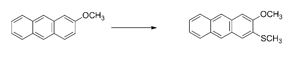
化合物(1)である、2-メトキシアントラセン(15.0g、72mmol)のTHF(520ml)溶液に、1.67Mのn-BuLi(86ml、144mmol)ヘキサン溶液を0℃で加えた。これを1時間室温で攪拌後、ジメチルジスルフィド(13ml、150mmol)を0℃で加え7時間室温で攪拌した。混合物を水(100ml)に投入し、THFをエバポレータで濃縮し、析出した結晶をろ別した。ろ過して水(100ml)、その後メタノール(100ml)で洗浄し、化合物(2)である3-メチルチオ-2-メトキシアントラセン(18.3g,定量的)を白色結晶として得た。
mp 176.5~177.5 ℃; 1H NMR (400 MHz, CDCl3) δ 2.58 (s, 3H), 4.03 (s, 3H), 7.16 (s, 1H), 7.39 (ddd, J = 8.2, 4.9, 1.9 Hz, 1H), 7.42 (ddd, J = 8.2, 4.9, 1.9 Hz, 1H), 7.55 (s, 1H), 7.92 (d, J = 9.5 Hz, 1H) 7.93 (d, J = 9.5 Hz, 1H), 8.22 (s, 1H), 8.24 (s, 1H); 13C NMR (125 MHz, CDCl3) δ 14.7, 56.2, 103.4, 122.5, 124.3, 124.7, 124.9, 125.4, 127.9, 128.4, 128.9, 131.0, 131.0, 131.7, 131.8, 154.6; EIMS (70 eV) m/z = 254 (M+). Anal Calcd for C16H14OS: C, 75.55; H, 5.55%. Found: C, 75.26; H, 5.33%. (I) Synthesis of 3-methylthio-2-methoxyanthracene
To a solution of compound (1), 2-methoxyanthracene (15.0 g, 72 mmol) in THF (520 ml), a 1.67 M n-BuLi (86 ml, 144 mmol) hexane solution was added at 0 ° C. After stirring this at room temperature for 1 hour, dimethyl disulfide (13 ml, 150 mmol) was added at 0 ° C. and stirred at room temperature for 7 hours. The mixture was poured into water (100 ml), THF was concentrated with an evaporator, and the precipitated crystals were separated by filtration. Filtration and washing with water (100 ml) and then methanol (100 ml) gave 3-methylthio-2-methoxyanthracene (18.3 g, quantitative) as compound (2) as white crystals.
mp 176.5-177.5 ° C; 1 H NMR (400 MHz, CDCl 3 ) δ 2.58 (s, 3H), 4.03 (s, 3H), 7.16 (s, 1H), 7.39 (ddd, J = 8.2, 4.9, 1.9 Hz , 1H), 7.42 (ddd, J = 8.2, 4.9, 1.9 Hz, 1H), 7.55 (s, 1H), 7.92 (d, J = 9.5 Hz, 1H) 7.93 (d, J = 9.5 Hz, 1H), 8.22 (s, 1H), 8.24 (s, 1H); 13 C NMR (125 MHz, CDCl 3 ) δ 14.7, 56.2, 103.4, 122.5, 124.3, 124.7, 124.9, 125.4, 127.9, 128.4, 128.9, 131.0, 131.0 , 131.7, 131.8, 154.6; EIMS (70 eV) m / z = 254 (M + ). Anal Calcd for C 16 H 14 OS: C, 75.55; H, 5.55%. Found: C, 75.26; H, 5.33% .
(II) 2-ヒドロキシ-3-メチルチオアントラセンの合成

3-メチルチオ-2-メトキシアントラセン(14.5g,57mmol)のジクロロメタン(200ml)溶液にBBr3(ca.2M,50ml,100mmol)のジクロロメタン溶液を-78℃で滴下した。5時間室温で攪拌した後、氷(約50g)を0℃で加えた。混合物をジクロロメタン(200ml×3)で抽出し、飽和食塩水(100ml×3)で洗浄し、MgSO4で乾燥して濃縮し、2-ヒドロキシ-3-メチルチオアントラセン(13.7g,定量的)を白色結晶として得た。
mp 175.6~176.5℃; 1H NMR (400 MHz, CDCl3) δ 2.49 (s, 3H), 6.54 (s, 1H), 7.31 (s, 1H), 7.39 (ddd, J = 10.7, 6.6, 1.4 Hz, 1H), 7.41 (s, 1H), 7.43 (ddd, J = 10.7, 6.6, 1.4 Hz, 1H), 7.91 (d, J = 8.8 Hz, 1H), 7.93 (dd, J = 8.8 1H), 8.14 (s, 1H), 8.22 (s, 1H), 8.30 (s, 1H); 13C NMR (100 MHz, CDCl3) δ 19.8, 107.8, 124.2, 125.0, 126.2, 126.2, 126.8, 128.0, 128.5, 128.6, 130.8, 132.8, 133.0, 133.8, 151.7; IR (KBr) ν3510 cm-1 (OH); EIMS (70 eV) m/z = 240 (M+); Anal Calcd for C15H12OS: C, 74.66; H, 4.72%. Found: C, 74.70; H, 4.84%. (II) Synthesis of 2-hydroxy-3-methylthioanthracene
A solution of BBr 3 (ca.2M, 50 ml, 100 mmol) in dichloromethane (200 ml) in 3-methylthio-2-methoxyanthracene (14.5 g, 57 mmol) was added dropwise at −78 ° C. After stirring for 5 hours at room temperature, ice (about 50 g) was added at 0 ° C. The mixture was extracted with dichloromethane (200 ml × 3), washed with saturated brine (100 ml × 3), dried over MgSO 4 and concentrated to give 2-hydroxy-3-methylthioanthracene (13.7 g, quantitative). Obtained as white crystals.
mp 175.6-176.5 ° C; 1 H NMR (400 MHz, CDCl 3 ) δ 2.49 (s, 3H), 6.54 (s, 1H), 7.31 (s, 1H), 7.39 (ddd, J = 10.7, 6.6, 1.4 Hz , 1H), 7.41 (s, 1H), 7.43 (ddd, J = 10.7, 6.6, 1.4 Hz, 1H), 7.91 (d, J = 8.8 Hz, 1H), 7.93 (dd, J = 8.8 1H), 8.14 (s, 1H), 8.22 (s, 1H), 8.30 (s, 1H); 13 C NMR (100 MHz, CDCl 3 ) δ 19.8, 107.8, 124.2, 125.0, 126.2, 126.2, 126.8, 128.0, 128.5, 128.6 , 130.8, 132.8, 133.0, 133.8, 151.7; IR (KBr) ν3510 cm -1 (OH); EIMS (70 eV) m / z = 240 (M + ); Anal Calcd for C 15 H 12 OS: C, 74.66 ; H, 4.72%. Found: C, 74.70; H, 4.84%.
(III) 3-(メチルチオ)アントラセン-2-イル トリフルオロメタンスルフォネートの合成

2-ヒドロキシ-3-メチルチオアントラセン(10.1g,42mmol)と、トリエチルアミン(16.0ml,115mmol)のジクロロメタン(400ml)溶液にトリフルオロメタンスルホン酸無水物(10.0ml,54.6mmol)を0℃で加えた。42時間室温で攪拌し水(50ml)で希釈した後、希塩酸(4M,100ml)を加えた。これをジクロロメタン(100ml×3)で抽出し、3回の抽出により得られた有機層を合わせて、飽和食塩水(100ml×3)で洗浄し、MgSO4で乾燥し、濃縮して3-(メチルチオ)アントラセン-2-イル トリフルオロメタンスルフォネート(15.5g,定量的)を黄色固体として得た。
mp 105.5~106.0℃; 1H NMR (400 MHz, CDCl3) δ 2.63 (s, 3H), 7.50 (ddd, J = 9.6, 6.3, 1.8 Hz, 1H), 7.51 (ddd, J = 9.6, 6.3, 1.8 Hz, 1H), 7.78 (s, 1H), 7.88 (s, 1H), 7.97 (dd, J = 5.5, 2.0 Hz, 1H), 7.98 (dd, J = 5.5, 2.0 Hz, 1H), 8.34 (s, 1H), 8.38 (s, 1H); 13C NMR (125 MHz, CDCl3) δ 15.8, 119.0, (q, J = 319 Hz), 119.5, 125.4, 126.2, 126.4, 126.8, 127.1, 128.4(×2), 129.0, 130.6, 131.0, 132.0, 132.9, 145.3; IR (KBr) ν 1429, 1207 cm-1 (-O-SO2-); EIMS (70 eV) m/z = 372 (M+); Anal Calcd for C16H11F3O3S2: C, 51.61; H, 2.98%. Found C, 51.57; H, 2.67%. (III) Synthesis of 3- (methylthio) anthracen-2-yl trifluoromethanesulfonate
To a solution of 2-hydroxy-3-methylthioanthracene (10.1 g, 42 mmol) and triethylamine (16.0 ml, 115 mmol) in dichloromethane (400 ml) was added trifluoromethanesulfonic anhydride (10.0 ml, 54.6 mmol) at 0 ° C. Added in. After stirring at room temperature for 42 hours and diluting with water (50 ml), dilute hydrochloric acid (4M, 100 ml) was added. This was extracted with dichloromethane (100 ml × 3), and the organic layers obtained by the extraction three times were combined, washed with saturated brine (100 ml × 3), dried over MgSO 4 , concentrated, and 3- ( Methylthio) anthracen-2-yl trifluoromethanesulfonate (15.5 g, quantitative) was obtained as a yellow solid.
mp 105.5-106.0 ° C; 1 H NMR (400 MHz, CDCl 3 ) δ 2.63 (s, 3H), 7.50 (ddd, J = 9.6, 6.3, 1.8 Hz, 1H), 7.51 (ddd, J = 9.6, 6.3, 1.8 Hz, 1H), 7.78 (s, 1H), 7.88 (s, 1H), 7.97 (dd, J = 5.5, 2.0 Hz, 1H), 7.98 (dd, J = 5.5, 2.0 Hz, 1H), 8.34 ( s, 1H), 8.38 (s, 1H); 13 C NMR (125 MHz, CDCl 3 ) δ 15.8, 119.0, (q, J = 319 Hz), 119.5, 125.4, 126.2, 126.4, 126.8, 127.1, 128.4 ( × 2), 129.0, 130.6, 131.0, 132.0, 132.9, 145.3; IR (KBr) ν 1429, 1207 cm -1 (-O-SO 2- ); EIMS (70 eV) m / z = 372 (M + ) ; Anal Calcd for C 16 H 11 F 3 O 3 S 2 : C, 51.61; H, 2.98%. Found C, 51.57; H, 2.67%.
(IV) トリブチルスタニルアセチレンの合成

窒素雰囲気下、18w%Naアセチレンのキシレンとミネラルオイルのディスパージョンオイル(10ml,8.5g,32mmol)のTHF(60ml)溶液にトリブチルチンクロリド(8.6ml、32mmol)を0℃で加えた。17時間室温で攪拌した後、混合物をヘキサンで抽出し食塩水で洗浄した。有機層を混合しMgSO4で乾燥したのち濃縮した。減圧蒸留(85~120℃、約0.7mmHg)して、トリブチルスタニルアセチレン(3.6g,34%)を無色油状物質として得た。
1H-NMR(400 MHz, CDCl3) δ 0.91(t, 9H, J = 8.0 Hz), 1.02(t, 8H, J = 8.0 Hz), 1.35(sextet, 6H, J = 8.0 Hz), 1.58(quintet,6H, J = 8.0 Hz), 2.20(s,1H) (IV) Synthesis of tributylstannylacetylene
Under a nitrogen atmosphere, tributyltin chloride (8.6 ml, 32 mmol) was added at 0 ° C. to a solution of 18 w% Na acetylene in xylene and mineral oil dispersion oil (10 ml, 8.5 g, 32 mmol) in THF (60 ml). After stirring for 17 hours at room temperature, the mixture was extracted with hexane and washed with brine. The organic layers were combined, dried over MgSO 4 and concentrated. Distillation under reduced pressure (85-120 ° C., about 0.7 mmHg) gave tributylstannylacetylene (3.6 g, 34%) as a colorless oil.
1 H-NMR (400 MHz, CDCl 3 ) δ 0.91 (t, 9H, J = 8.0 Hz), 1.02 (t, 8H, J = 8.0 Hz), 1.35 (sextet, 6H, J = 8.0 Hz), 1.58 ( quintet, 6H, J = 8.0 Hz), 2.20 (s, 1H)
(V) 1,2-ビス(トリブチルスタニル)エチレン(化合物(3)-05)の合成

窒素雰囲気下、トリブチルスタニルアセチレン(1.6g,5mmol)と、トリブチルチンハイドライド(1.3ml,5mmol)とのトルエン(20ml)溶液にアゾビスイソブチロニトリル(100mg,0.60mmol)を加えた。この混合物を17時間、90℃で加熱攪拌し、水(20ml)を加えたのち濃縮した。混合物をヘキサンで抽出し、抽出液を食塩水で洗浄して1,2-ビス(トリブチルスタニル)エチレン(化合物(3)-05)(3.0g,90%)を無色油状物質として得た。
1H-NMR(400 MHz, CDCl3) δ 0.86-0.91(multiplet, 15H), 1.31(sextet, 6H, J = 8.0 Hz), 1.50(quintet,6H, J = 8.0 Hz), 6.88(s,2H) (V) Synthesis of 1,2-bis (tributylstannyl) ethylene (compound (3) -05)
Under a nitrogen atmosphere, azobisisobutyronitrile (100 mg, 0.60 mmol) was added to a toluene (20 ml) solution of tributylstannylacetylene (1.6 g, 5 mmol) and tributyltin hydride (1.3 ml, 5 mmol). It was. The mixture was stirred with heating at 90 ° C. for 17 hours, water (20 ml) was added, and the mixture was concentrated. The mixture was extracted with hexane, and the extract was washed with brine to give 1,2-bis (tributylstannyl) ethylene (compound (3) -05) (3.0 g, 90%) as a colorless oil. .
1 H-NMR (400 MHz, CDCl 3 ) δ 0.86-0.91 (multiplet, 15H), 1.31 (sextet, 6H, J = 8.0 Hz), 1.50 (quintet, 6H, J = 8.0 Hz), 6.88 (s, 2H )
(VI) trans-1,2-ビス(3-メチルチオアントラセン-2-イル)エタンの合成

窒素雰囲気下で、3-(メチルチオ)アントラセン-2-イル トリフルオロメタンスルフォネート(11.2g,30mmol)と、1,2-ビス(トリブチルスタニル)エチレン(化合物(5)-05)(9.1g,15.0mmol)のDMF(110ml)溶液に、Pd(PPh3)4(1.2g,1.0mmol,3mol%)を加え100℃で17時間暗所で加熱した。冷却して水で薄め、析出した結晶をろ別し、水(100ml)、エタノール(50ml)で洗浄して、化合物(4)であるtrans-1,2-ビス(3-メチルチオアントラセン-2-イル)エタン(3.9g,55%)を黄色固体として得た。
mp > 300℃; 1H NMR (400 MHz, CDCl3)δ 2.66 (s, 6H), 7.44 (dd, J = 5.0, 4.4 Hz, 4H), 7.75 (s, 2H), 7.78 (s, 2H), 7.97 (d, J = 9.6 Hz, 2H), 7.98 (d, J = 9.6 Hz, 2H), 8.27 (s, 2H), 8.30 (s, 2H) , 8.44 (s, 2H); 13C NMR (100 MHz, CDCl3) δ 16.8, 124.2, 124.9, 125.7, 125.7, 126.0, 126.8, 126.9, 128.5, 128.6, 129.2, 130.6, 132.0, 132.8, 136.5, 147.3; IR (KBr) 1485, 1426, 1024, 957, 862, 741 cm-1; EIMS (70 eV) m/z = 472 (M+); Anal Calcd for C32H24S2: C, 81.31; H, 5.12%. Found: C, 81.21; H, 4.90%. (VI) Synthesis of trans-1,2-bis (3-methylthioanthracen-2-yl) ethane
Under a nitrogen atmosphere, 3- (methylthio) anthracen-2-yl trifluoromethanesulfonate (11.2 g, 30 mmol) and 1,2-bis (tributylstannyl) ethylene (compound (5) -05) (9 0.1 g, 15.0 mmol) in DMF (110 ml) was added Pd (PPh 3 ) 4 (1.2 g, 1.0 mmol, 3 mol%) and heated at 100 ° C. for 17 hours in the dark. After cooling and diluting with water, the precipitated crystals were filtered off, washed with water (100 ml) and ethanol (50 ml), and the compound (4) trans-1,2-bis (3-methylthioanthracene-2- Yl) ethane (3.9 g, 55%) was obtained as a yellow solid.
mp> 300 ° C; 1 H NMR (400 MHz, CDCl 3 ) δ 2.66 (s, 6H), 7.44 (dd, J = 5.0, 4.4 Hz, 4H), 7.75 (s, 2H), 7.78 (s, 2H) , 7.97 (d, J = 9.6 Hz, 2H), 7.98 (d, J = 9.6 Hz, 2H), 8.27 (s, 2H), 8.30 (s, 2H), 8.44 (s, 2H); 13 C NMR ( 100 MHz, CDCl 3 ) δ 16.8, 124.2, 124.9, 125.7, 125.7, 126.0, 126.8, 126.9, 128.5, 128.6, 129.2, 130.6, 132.0, 132.8, 136.5, 147.3; IR (KBr) 1485, 1426, 1024, 957 , 862, 741 cm -1 ; EIMS (70 eV) m / z = 472 (M + ); Anal Calcd for C 32 H 24 S 2 : C, 81.31; H, 5.12%. Found: C, 81.21; H, 4.90%.
(VII) ジアントラ[2,3-b:2’,3’-f]チエノ[3,2-b]チオフェンの合成

粉末状にすりつぶしたヨウ素(59g,232mmol)と、trans-1,2-ビス(3-メチルチオアントラセン-2-イル)エタン(3.8g,8.0mmol)とを、酢酸(250ml)に加え、11時間加熱還流した。過剰な酢酸を蒸留にて除去し、飽和NaHSO3水溶液(200ml)を加え、1時間攪拌した。ろ別して結晶を水(100ml)、アセトン(100ml)、ジクロロメタン(100ml)で洗浄してジアントラ[2,3-b:2’,3’-f]チエノ[3,2-b]チオフェン(DATT)(3.8g,定量的)を濃赤色固体として得た。昇華精製を行い(約400℃、10-2Pa以下、窒素気流下)、クロロベンゼンから再結晶し収率50%でジアントラ[2,3-b:2’,3’-f]チエノ[3,2-b]チオフェンを得た。
mp.>300℃;
EIMS (70 eV) m/z = 440 (M+). Anal Calcd for C30H16S2: C, 81.78; H, 3.66%. Found: C, 81.38; H, 3.52%. λmax=550-570nm(薄膜時)。 (VII) Synthesis of diantra [2,3-b: 2 ′, 3′-f] thieno [3,2-b] thiophene
Powdered iodine (59 g, 232 mmol) and trans-1,2-bis (3-methylthioanthracen-2-yl) ethane (3.8 g, 8.0 mmol) were added to acetic acid (250 ml), Heated to reflux for 11 hours. Excess acetic acid was removed by distillation, saturated aqueous NaHSO 3 solution (200 ml) was added, and the mixture was stirred for 1 hr. The crystals were separated by filtration, washed with water (100 ml), acetone (100 ml), dichloromethane (100 ml) and washed with dianthra [2,3-b: 2 ′, 3′-f] thieno [3,2-b] thiophene (DATT). (3.8 g, quantitative) was obtained as a dark red solid. Sublimation purification is performed (about 400 ° C., 10 −2 Pa or less, under a nitrogen stream), recrystallization from chlorobenzene, and 50% yield of dianthra [2,3-b: 2 ′, 3′-f] thieno [3, 2-b] thiophene was obtained.
mp. > 300 ° C;
EIMS (70 eV) m / z = 440 (M + ). Anal Calcd for C 30 H 16 S 2 : C, 81.78; H, 3.66%. Found: C, 81.38; H, 3.52%. Λmax = 550-570nm (When thin).
比較例1
特許文献3にならって下記反応式(4)に従い、ジアントラ[2,3-b:2’,3’-f]チエノ[3,2-b]チオフェンの合成を行った。
反応式(4-1)では目的物化合物の3-(メチルチオ)アントラセン-2-カルボアルデヒドが1位にメチルチオ基が導入された異性体との混合物として収率80%で得られた。プロトンNMRによる同定から、目的物(3位)と副生物(1位)とは4:1の比率での混合物であった。この混合物を用いて反応式(4-2)に示すカップリング反応を行い、目的物のTrans-1,2-ビス(3-メチルチオアントラセン-2-イル)エタンを約50%の純度(プロトンNMRより同定)で含む粗成物を得た。最後に反応式(4-3)に示す環化反応によりジアントラ[2,3-b:2’,3’-f]チエノ[3,2-b]チオフェンを含む粗生成物を得た。これらを昇華精製及び再結晶を繰り返すことにより目的化合物を得たが、本願の製造方法に比べ、中間体不純物が非常に多く、最終的な総収率で大きく劣るほか、それらを取り除くための精製工程が非常に煩雑であった。

Comparative Example 1
According to the following reaction formula (4) followingPatent Document 3, dianthra [2,3-b: 2 ′, 3′-f] thieno [3,2-b] thiophene was synthesized.
In the reaction formula (4-1), the target compound 3- (methylthio) anthracene-2-carbaldehyde was obtained in a yield of 80% as a mixture with an isomer having a methylthio group introduced at the 1-position. From identification by proton NMR, the target product (position 3) and by-product (position 1) were a mixture in a ratio of 4: 1. Using this mixture, a coupling reaction shown in the reaction formula (4-2) was performed, and the target product Trans-1,2-bis (3-methylthioanthracen-2-yl) ethane was purified to about 50% purity (proton NMR). The crude product contained in (identification) was obtained. Finally, a crude product containing dianthra [2,3-b: 2 ′, 3′-f] thieno [3,2-b] thiophene was obtained by a cyclization reaction shown in the reaction formula (4-3). These compounds were obtained by repeating sublimation purification and recrystallization. However, compared with the production method of the present application, the amount of intermediate impurities was very large, and the final total yield was greatly inferior. In addition, purification to remove them was performed. The process was very complicated.
特許文献3にならって下記反応式(4)に従い、ジアントラ[2,3-b:2’,3’-f]チエノ[3,2-b]チオフェンの合成を行った。
反応式(4-1)では目的物化合物の3-(メチルチオ)アントラセン-2-カルボアルデヒドが1位にメチルチオ基が導入された異性体との混合物として収率80%で得られた。プロトンNMRによる同定から、目的物(3位)と副生物(1位)とは4:1の比率での混合物であった。この混合物を用いて反応式(4-2)に示すカップリング反応を行い、目的物のTrans-1,2-ビス(3-メチルチオアントラセン-2-イル)エタンを約50%の純度(プロトンNMRより同定)で含む粗成物を得た。最後に反応式(4-3)に示す環化反応によりジアントラ[2,3-b:2’,3’-f]チエノ[3,2-b]チオフェンを含む粗生成物を得た。これらを昇華精製及び再結晶を繰り返すことにより目的化合物を得たが、本願の製造方法に比べ、中間体不純物が非常に多く、最終的な総収率で大きく劣るほか、それらを取り除くための精製工程が非常に煩雑であった。
According to the following reaction formula (4) following
In the reaction formula (4-1), the target compound 3- (methylthio) anthracene-2-carbaldehyde was obtained in a yield of 80% as a mixture with an isomer having a methylthio group introduced at the 1-position. From identification by proton NMR, the target product (position 3) and by-product (position 1) were a mixture in a ratio of 4: 1. Using this mixture, a coupling reaction shown in the reaction formula (4-2) was performed, and the target product Trans-1,2-bis (3-methylthioanthracen-2-yl) ethane was purified to about 50% purity (proton NMR). The crude product contained in (identification) was obtained. Finally, a crude product containing dianthra [2,3-b: 2 ′, 3′-f] thieno [3,2-b] thiophene was obtained by a cyclization reaction shown in the reaction formula (4-3). These compounds were obtained by repeating sublimation purification and recrystallization. However, compared with the production method of the present application, the amount of intermediate impurities was very large, and the final total yield was greatly inferior. In addition, purification to remove them was performed. The process was very complicated.
以上のように、本発明により、ジアントラ[2,3-b:2’,3’-f]チエノ[3,2-b]チオフェンを簡便かつ効率的に合成することが可能となった。
As described above, according to the present invention, diantra [2,3-b: 2 ', 3'-f] thieno [3,2-b] thiophene can be synthesized easily and efficiently.
次にジアントラ[2,3-b:2’,3’-f]チエノ[3,2-b]チオフェンからなる半導体層を有する電界効果トランジスタについて詳細に説明する。
Next, a field effect transistor having a semiconductor layer made of dianthra [2,3-b: 2 ', 3'-f] thieno [3,2-b] thiophene will be described in detail.
実施例2(トップコンタクト型電界効果トランジスタ)
オクタデシルトリクロロシラン処理を行った300nmのSiO2熱酸化膜付きnドープシリコンウェハー(面抵抗0.02Ω・cm以下)を真空蒸着装置内に設置し、装置内の真空度が3.0×10⁻³Pa以下になるまで排気した。抵抗加熱蒸着法によって、この電極に基板温度約100℃の条件下で、実施例1で得られたジアントラ[2,3-b:2’,3’-f]チエノ[3,2-b]チオフェンを25nmの厚さに蒸着し、半導体層(2)を形成した。次いでこの基板に電極作製用シャドウマスクを取り付け、真空蒸着装置内に設置し、装置内の真空度が1.0×10⁻⁴Pa以下になるまで排気し、抵抗加熱蒸着法によって、金の電極、すなわちソース電極(1)及びドレイン電極(3)、を40nmの厚さに蒸着し、TC(トップコンタクト)型である本発明の電界効果トランジスタを得た。
なお、本実施例における電界効果トランジスタにおいては、熱酸化膜付きnドープシリコンウェハーにおける熱酸化膜が絶縁層(4)の機能を有し、nドープシリコンウェハーが基板(6)及びゲート電極(5)の機能を兼ね備えている。
得られた電界効果トランジスタをプローバー内に設置し半導体パラメーターアナライザー4155C(Agilent社製)を用いて半導体特性を測定した。半導体特性はゲート電圧を10V~-100Vまで20Vステップで走査し、またドレイン電圧を10V~-100Vまで走査し、ドレイン電流-ドレイン電圧を測定した。その結果、電流飽和が観測され、得られた電圧電流曲線より、本素子はp型半導体を示し、キャリア移動度は2.5~3.0cm2/Vsであった。 Example 2 (Top Contact Field Effect Transistor)
An n-doped silicon wafer with 300 nm SiO 2 thermal oxide film (surface resistance 0.02 Ω · cm or less) treated with octadecyltrichlorosilane was placed in a vacuum deposition apparatus, and the degree of vacuum in the apparatus was 3.0 × 10 −. It exhausted until it became 3 Pa or less. The dianthra [2,3-b: 2 ′, 3′-f] thieno [3,2-b] obtained in Example 1 was applied to this electrode under the condition of a substrate temperature of about 100 ° C. by resistance heating vapor deposition. Thiophene was deposited to a thickness of 25 nm to form a semiconductor layer (2). Next, a shadow mask for electrode preparation is attached to this substrate, placed in a vacuum vapor deposition apparatus, evacuated until the degree of vacuum in the apparatus is 1.0 × 10 −4 Pa or less, and gold electrode is formed by resistance heating vapor deposition That is, the source electrode (1) and the drain electrode (3) were vapor-deposited to a thickness of 40 nm to obtain a TC (top contact) type field effect transistor of the present invention.
In the field effect transistor of this example, the thermal oxide film in the n-doped silicon wafer with the thermal oxide film has the function of the insulating layer (4), and the n-doped silicon wafer is the substrate (6) and the gate electrode (5). )
The obtained field effect transistor was installed in a prober, and semiconductor characteristics were measured using a semiconductor parameter analyzer 4155C (manufactured by Agilent). For semiconductor characteristics, the gate voltage was scanned from 10 V to -100 V in 20 V steps, the drain voltage was scanned from 10 V to -100 V, and the drain current-drain voltage was measured. As a result, current saturation was observed, and from the obtained voltage-current curve, the device showed a p-type semiconductor, and the carrier mobility was 2.5 to 3.0 cm 2 / Vs.
次にジアントラ[2,3-b:2’,3’-f]チエノ[3,2-b]チオフェンからなる半導体層を有する有機太陽電池素子について詳細に説明する。
Next, an organic solar cell element having a semiconductor layer made of dianthra [2,3-b: 2 ′, 3′-f] thieno [3,2-b] thiophene will be described in detail.
実施例3
ITO透明導電膜を115nm堆積させたガラス基板(東京三容真空(株)製、20Ω/□以下)を素子作製前にUV-オゾン洗浄した。このガラス基板を真空蒸着装置内に設置し、装置内の真空度が3.0×10-3Pa以下になるまで排気した。抵抗加熱蒸着法によって、この電極に実施例1で得られたジアントラ[2,3-b:2’,3’-f]チエノ[3,2-b]チオフェンを40nmの厚さに蒸着し、半導体層を形成した。次いでC60を40nmの厚さに、2,9-ジメチル-4,7-ジフェニル-1,10-フェナントロリンを10nmの厚さで蒸着した。さらにシャドウマスクを介してアルミニウムを100nmの厚さに蒸着して陰極を形成し、φ2mmの丸型有機太陽電池素子を作製した。AM1.5のソーラーシミュレーターを用いて100mW/cmとして光電変換効率を測定した。開放電圧は0.42V、短絡電流は5.04mA/cm2、フィルファクターは0.56、変換効率は1.19%の有機太陽電池が得られた。図4に本実施例の有機太陽電池素子のJ-V特性図を示す。 Example 3
A glass substrate (manufactured by Tokyo Sanyo Vacuum Co., Ltd., 20Ω / □ or less) on which an ITO transparent conductive film was deposited to 115 nm was UV-ozone cleaned before device fabrication. This glass substrate was placed in a vacuum vapor deposition apparatus and evacuated until the degree of vacuum in the apparatus became 3.0 × 10 −3 Pa or less. The dianthra [2,3-b: 2 ′, 3′-f] thieno [3,2-b] thiophene obtained in Example 1 was deposited on this electrode to a thickness of 40 nm by resistance heating evaporation. A semiconductor layer was formed. Next, C60 was deposited to a thickness of 40 nm, and 2,9-dimethyl-4,7-diphenyl-1,10-phenanthroline was deposited to a thickness of 10 nm. Further, aluminum was deposited to a thickness of 100 nm through a shadow mask to form a cathode, and a φ2 mm round organic solar cell element was produced. The photoelectric conversion efficiency was measured at 100 mW / cm using an AM1.5 solar simulator. An organic solar cell with an open-circuit voltage of 0.42 V, a short-circuit current of 5.04 mA / cm 2 , a fill factor of 0.56, and a conversion efficiency of 1.19% was obtained. FIG. 4 shows a JV characteristic diagram of the organic solar cell element of this example.
以上のように、有機電界効果トランジスタ及び有機薄膜太陽電池素子を作製し、その実用性が確認できた。本発明により簡便かつ効率的に得られたジアントラ[2,3-b:2’,3’-f]チエノ[3,2-b]チオフェンは優れた特性値をもつため、有機電界効果トランジスタ、有機発光ダイオード、有機発光トランジスタ、有機太陽電池、有機レーザー、有機光センサー等、様々な有機エレクトロニクスデバイス用の材料として非常に有用な化合物であるといえる。
As described above, organic field effect transistors and organic thin-film solar cell elements were produced and their practicality was confirmed. Since dianthra [2,3-b: 2 ′, 3′-f] thieno [3,2-b] thiophene obtained simply and efficiently according to the present invention has excellent characteristic values, organic field effect transistors, It can be said that it is a very useful compound as a material for various organic electronic devices such as organic light emitting diodes, organic light emitting transistors, organic solar cells, organic lasers, and organic optical sensors.
図1において同じ名称には同じ番号を付すものとする。
1 ソース電極
2 半導体層
3 ドレイン電極
4 絶縁体層
5 ゲート電極
6 基板
7 保護層 In FIG. 1, the same numbers are assigned to the same names.
1source electrode 2 semiconductor layer 3 drain electrode 4 insulator layer 5 gate electrode 6 substrate 7 protective layer
1 ソース電極
2 半導体層
3 ドレイン電極
4 絶縁体層
5 ゲート電極
6 基板
7 保護層 In FIG. 1, the same numbers are assigned to the same names.
1
Claims (11)
- ジアントラ[2,3-b:2’,3’-f]チエノ[3,2-b]チオフェンを製造する方法であって、
式(1)で表される化合物と、ジメチルスルフィドとを反応させ、式(2)で表される化合物を得る工程;
式(2)で表される化合物と、式(3)で表わされるスズ化合物とを反応させて、式(4)で表される化合物を得る工程;及び
式(4)で表される化合物を環化させ、ジアントラ[2,3-b:2’,3’-f]チエノ[3,2-b]チオフェンを得る工程;
を含む、上記方法。


(式中、R1、R2は置換基を表し、Meはメチル基を表す。) A process for producing diantra [2,3-b: 2 ′, 3′-f] thieno [3,2-b] thiophene, comprising:
A step of reacting a compound represented by the formula (1) with dimethyl sulfide to obtain a compound represented by the formula (2);
Reacting a compound represented by the formula (2) with a tin compound represented by the formula (3) to obtain a compound represented by the formula (4); and a compound represented by the formula (4) Cyclization to obtain diantra [2,3-b: 2 ′, 3′-f] thieno [3,2-b] thiophene;
Including the above method.
(In the formula, R 1 and R 2 represent a substituent, and Me represents a methyl group.) - 請求項1に記載の方法により得られたジアントラ[2,3-b:2’,3’-f]チエノ[3,2-b]チオフェンを含む有機半導体材料。 An organic semiconductor material containing diantra [2,3-b: 2 ', 3'-f] thieno [3,2-b] thiophene obtained by the method according to claim 1.
- 請求項1に記載の方法により得られたジアントラ[2,3-b:2’,3’-f]チエノ[3,2-b]チオフェンを含有する半導体デバイス作製用インク。 An ink for producing a semiconductor device comprising diantra [2,3-b: 2 ', 3'-f] thieno [3,2-b] thiophene obtained by the method according to claim 1.
- 請求項1に記載の方法により得られたジアントラ[2,3-b:2’,3’-f]チエノ[3,2-b]チオフェンを含有する有機半導体薄膜。 An organic semiconductor thin film containing diantra [2,3-b: 2 ', 3'-f] thieno [3,2-b] thiophene obtained by the method according to claim 1.
- 請求項4に記載の有機半導体薄膜を有する有機エレクトロニクスデバイス。 An organic electronic device having the organic semiconductor thin film according to claim 4.
- 光電変換素子、有機EL素子、有機半導体レーザー素子、液晶表示素子又は薄膜トランジスタ素子である、請求項5に記載の有機エレクトロニクスデバイス。 The organic electronics device according to claim 5, which is a photoelectric conversion element, an organic EL element, an organic semiconductor laser element, a liquid crystal display element or a thin film transistor element.
- 太陽電池である、請求項5に記載の有機エレクトロニクスデバイス。 The organic electronic device according to claim 5, which is a solar cell.
- 光センサーである、請求項5に記載の有機エレクトロニクスデバイス。 The organic electronic device according to claim 5, which is an optical sensor.
- 請求項1に記載の方法により得られたジアントラ[2,3-b:2’,3’-f]チエノ[3,2-b]チオフェンからなる半導体層を基板上に形成する工程を含む請求項5に記載の有機エレクトロニクスデバイスの製造方法。 A process comprising: forming a semiconductor layer made of dianthra [2,3-b: 2 ′, 3′-f] thieno [3,2-b] thiophene obtained by the method according to claim 1 on a substrate. Item 6. A method for producing an organic electronic device according to Item 5.
- 半導体層が蒸着法により形成される請求項9に記載の有機エレクトロニクスデバイスの製造方法。 The method for producing an organic electronic device according to claim 9, wherein the semiconductor layer is formed by a vapor deposition method.
- 請求項3に記載の半導体デバイス作製用インクを塗布することによって半導体層を形成する請求項9に記載の有機エレクトロニクスデバイスの製造方法。 The method for producing an organic electronic device according to claim 9, wherein the semiconductor layer is formed by applying the ink for producing a semiconductor device according to claim 3.
Priority Applications (1)
| Application Number | Priority Date | Filing Date | Title |
|---|---|---|---|
| JP2012539130A JPWO2012115218A1 (en) | 2011-02-25 | 2012-02-24 | Process for producing diantra [2,3-b: 2 ', 3'-f] thieno [3,2-b] thiophene and use thereof |
Applications Claiming Priority (2)
| Application Number | Priority Date | Filing Date | Title |
|---|---|---|---|
| JP2011-039404 | 2011-02-25 | ||
| JP2011039404 | 2011-02-25 |
Publications (1)
| Publication Number | Publication Date |
|---|---|
| WO2012115218A1 true WO2012115218A1 (en) | 2012-08-30 |
Family
ID=46720992
Family Applications (1)
| Application Number | Title | Priority Date | Filing Date |
|---|---|---|---|
| PCT/JP2012/054528 WO2012115218A1 (en) | 2011-02-25 | 2012-02-24 | Method for producing dianthra[2,3-b:2',3'-f]thieno[3,2-b]thiophene, and use thereof |
Country Status (3)
| Country | Link |
|---|---|
| JP (1) | JPWO2012115218A1 (en) |
| TW (1) | TW201247676A (en) |
| WO (1) | WO2012115218A1 (en) |
Cited By (5)
| Publication number | Priority date | Publication date | Assignee | Title |
|---|---|---|---|---|
| WO2018043763A1 (en) * | 2016-09-02 | 2018-03-08 | Kyushu University, National University Corporation | Continuous-wave organic thin-film distributed feedback laser and electrically driven organic semiconductor laser diode |
| KR20180026320A (en) * | 2016-09-02 | 2018-03-12 | 고쿠리쓰다이가쿠호진 규슈다이가쿠 | Continuous-wave organic thin-film distributed feedback laser and electrically driven organic semiconductor laser diode |
| WO2020039708A1 (en) | 2018-08-23 | 2020-02-27 | 国立大学法人九州大学 | Organic electroluminescence element |
| US11183815B2 (en) | 2017-02-07 | 2021-11-23 | Koala Tech Inc. | Current-injection organic semiconductor laser diode, meihod for producing same and program |
| WO2023189381A1 (en) * | 2022-03-30 | 2023-10-05 | ソニーグループ株式会社 | Light-emitting element and electronic device |
Families Citing this family (1)
| Publication number | Priority date | Publication date | Assignee | Title |
|---|---|---|---|---|
| CN104854719B (en) * | 2012-12-12 | 2018-11-13 | 株式会社大赛璐 | Organic transistor manufacture solvent or solvent compositions |
Citations (2)
| Publication number | Priority date | Publication date | Assignee | Title |
|---|---|---|---|---|
| WO2009009790A1 (en) * | 2007-07-12 | 2009-01-15 | President And Fellows Of Harvard College | Air-stable, high hole mobility thieno-thiophene derivatives |
| JP2011003852A (en) * | 2009-06-22 | 2011-01-06 | Asahi Kasei Corp | Organic semiconductor thin film with sheet-like crystal of condensed polycyclic aromatic compound containing sulfur atom laminated on substrate, and method of manufacturing the same |
-
2012
- 2012-02-24 TW TW101106272A patent/TW201247676A/en unknown
- 2012-02-24 WO PCT/JP2012/054528 patent/WO2012115218A1/en active Application Filing
- 2012-02-24 JP JP2012539130A patent/JPWO2012115218A1/en active Pending
Patent Citations (2)
| Publication number | Priority date | Publication date | Assignee | Title |
|---|---|---|---|---|
| WO2009009790A1 (en) * | 2007-07-12 | 2009-01-15 | President And Fellows Of Harvard College | Air-stable, high hole mobility thieno-thiophene derivatives |
| JP2011003852A (en) * | 2009-06-22 | 2011-01-06 | Asahi Kasei Corp | Organic semiconductor thin film with sheet-like crystal of condensed polycyclic aromatic compound containing sulfur atom laminated on substrate, and method of manufacturing the same |
Non-Patent Citations (1)
| Title |
|---|
| RICHARD A.H. ET AL.: "Palladium(0) catalyzed coupling of trans-1,2-Bis(tri-n-butylstannyl) ethylene with aromatic halides: A convenient synthesis of substituted trans-§-bromostyrenes.", TETRAHEDRON LETTERS, vol. 29, no. 23, 1988, pages 2783 - 2786 * |
Cited By (11)
| Publication number | Priority date | Publication date | Assignee | Title |
|---|---|---|---|---|
| WO2018043763A1 (en) * | 2016-09-02 | 2018-03-08 | Kyushu University, National University Corporation | Continuous-wave organic thin-film distributed feedback laser and electrically driven organic semiconductor laser diode |
| KR20180026320A (en) * | 2016-09-02 | 2018-03-12 | 고쿠리쓰다이가쿠호진 규슈다이가쿠 | Continuous-wave organic thin-film distributed feedback laser and electrically driven organic semiconductor laser diode |
| JP2019526937A (en) * | 2016-09-02 | 2019-09-19 | 国立大学法人九州大学 | Continuous wave organic thin film distributed feedback laser and electrically driven organic semiconductor laser diode |
| KR102402133B1 (en) * | 2016-09-02 | 2022-05-26 | 고쿠리쓰다이가쿠호진 규슈다이가쿠 | Continuous-wave organic thin-film distributed feedback laser and electrically driven organic semiconductor laser diode |
| US11539190B2 (en) | 2016-09-02 | 2022-12-27 | Kyushu University, National University Corporation | Continuous-wave organic thin-film distributed feedback laser and electrically driven organic semiconductor laser diode |
| US11909177B2 (en) | 2016-09-02 | 2024-02-20 | Kyushu University, National University Corporation | Continuous-wave organic thin-film distributed feedback laser and electrically driven organic semiconductor laser diode |
| US11183815B2 (en) | 2017-02-07 | 2021-11-23 | Koala Tech Inc. | Current-injection organic semiconductor laser diode, meihod for producing same and program |
| US11626710B2 (en) | 2017-02-07 | 2023-04-11 | Kyushu University, National University Corporation | Current-injection organic semiconductor laser diode, method for producing same and program |
| US11955776B2 (en) | 2017-02-07 | 2024-04-09 | Kyushu University, National University Corporation | Current-injection organic semiconductor laser diode, method for producing same and program |
| WO2020039708A1 (en) | 2018-08-23 | 2020-02-27 | 国立大学法人九州大学 | Organic electroluminescence element |
| WO2023189381A1 (en) * | 2022-03-30 | 2023-10-05 | ソニーグループ株式会社 | Light-emitting element and electronic device |
Also Published As
| Publication number | Publication date |
|---|---|
| JPWO2012115218A1 (en) | 2014-07-07 |
| TW201247676A (en) | 2012-12-01 |
Similar Documents
| Publication | Publication Date | Title |
|---|---|---|
| JP5622585B2 (en) | Novel heterocyclic compounds and their use | |
| JP6208133B2 (en) | Heterocyclic compounds and uses thereof | |
| WO2014061745A1 (en) | Novel condensed polycyclic aromatic compound and use thereof | |
| JP6558777B2 (en) | Organic compounds and their uses | |
| WO2012115218A1 (en) | Method for producing dianthra[2,3-b:2',3'-f]thieno[3,2-b]thiophene, and use thereof | |
| JP2016166284A (en) | Novel organic compound and use thereof | |
| JP6436590B2 (en) | Novel organic polycyclic aromatic compounds and uses thereof | |
| WO2013031468A1 (en) | Heterocyclic compound and use thereof | |
| JP6478278B2 (en) | Organic polycyclic aromatic compounds and uses thereof | |
| JP6425646B2 (en) | Novel condensed polycyclic aromatic compound and use thereof | |
| JP5600267B2 (en) | Novel compounds and their use | |
| WO2012165612A1 (en) | Organic semiconductor material, and organic electronics device | |
| JP6572473B2 (en) | Organic compounds and their uses | |
| JP6497560B2 (en) | Novel condensed polycyclic aromatic compounds and uses thereof | |
| JP6592863B2 (en) | Organic compounds and their uses | |
| JP6478279B2 (en) | Organic polycyclic aromatic compounds and uses thereof | |
| JP6478277B2 (en) | Organic polycyclic aromatic compounds and uses thereof |
Legal Events
| Date | Code | Title | Description |
|---|---|---|---|
| WWE | Wipo information: entry into national phase |
Ref document number: 2012539130 Country of ref document: JP |
|
| 121 | Ep: the epo has been informed by wipo that ep was designated in this application |
Ref document number: 12749714 Country of ref document: EP Kind code of ref document: A1 |
|
| NENP | Non-entry into the national phase |
Ref country code: DE |
|
| 122 | Ep: pct application non-entry in european phase |
Ref document number: 12749714 Country of ref document: EP Kind code of ref document: A1 |