以下、添付図面を参照しながら本発明による空間光変調装置および空間光変調方法の実施の形態を詳細に説明する。なお、図面の説明において同一の要素には同一の符号を付し、重複する説明を省略する。
Hereinafter, embodiments of a spatial light modulation device and a spatial light modulation method according to the present invention will be described in detail with reference to the accompanying drawings. In the description of the drawings, the same elements are denoted by the same reference numerals, and redundant description is omitted.
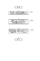
図1は、本発明の一実施形態に係る空間光変調装置1Aの構成を概略的に示すブロック図である。図1に示されるように、本実施形態の空間光変調装置1Aは、位相変調部10を備える。位相変調部10は、シリコン基板の上に液晶が形成された構成を有する、反射型の液晶表示パネル(いわゆるLCOS-SLM)である。この位相変調部10は、入射光の位相を変調する。また、空間光変調装置1Aは、電圧生成部50Aを備える。電圧生成部50Aは、駆動装置20A及び制御装置30Aによって構成されている。位相変調部10、駆動装置20A、及び制御装置30Aは、互いに独立した筐体にそれぞれ収容されている。
FIG. 1 is a block diagram schematically showing a configuration of a spatial light modulation device 1A according to an embodiment of the present invention. As shown in FIG. 1, the spatial light modulation device 1 </ b> A of this embodiment includes a phase modulation unit 10. The phase modulation unit 10 has a configuration in which liquid crystal is formed on a silicon substrate, a reflective liquid crystal display panel (so-called LCOS-SLM). The phase modulation unit 10 modulates the phase of incident light. The spatial light modulation device 1A includes a voltage generation unit 50A. The voltage generation unit 50A includes a drive device 20A and a control device 30A. The phase modulation unit 10, the driving device 20A, and the control device 30A are respectively housed in independent housings.
図2(a)は、位相変調部10の構成の一部を示す側断面図である。位相変調部10は、シリコン基板11と、シリコン基板11上に設けられた液晶層12とを有する。また、位相変調部10は、シリコン基板11と液晶層12との間に配置された第1の電極13、及び該第1の電極13との間に液晶層12を挟む位置に設けられた第2の電極14を更に有する。第1の電極13は、液晶層12に電圧を印加するための複数の画素電極13aを有している。複数の画素電極13aは、複数行および複数列にわたって二次元状に配置されており、これらの画素電極13aによって位相変調部10の複数の画素が規定される。第2の電極14は、ガラス基板15の一方の面上に蒸着された金属膜からなる。ガラス基板15は、上記一方の面とシリコン基板11とが対向するように、スペーサ16を介してシリコン基板11上に支持されている。液晶層12は、シリコン基板11とガラス基板15との間に液晶が充填されて成る。
FIG. 2A is a side sectional view showing a part of the configuration of the phase modulation unit 10. The phase modulation unit 10 includes a silicon substrate 11 and a liquid crystal layer 12 provided on the silicon substrate 11. The phase modulation unit 10 includes a first electrode 13 disposed between the silicon substrate 11 and the liquid crystal layer 12 and a first electrode 13 provided at a position sandwiching the liquid crystal layer 12 between the first electrode 13. Two electrodes 14 are further provided. The first electrode 13 has a plurality of pixel electrodes 13 a for applying a voltage to the liquid crystal layer 12. The plurality of pixel electrodes 13a are two-dimensionally arranged over a plurality of rows and a plurality of columns, and a plurality of pixels of the phase modulation unit 10 are defined by these pixel electrodes 13a. The second electrode 14 is made of a metal film deposited on one surface of the glass substrate 15. The glass substrate 15 is supported on the silicon substrate 11 via a spacer 16 so that the one surface and the silicon substrate 11 face each other. The liquid crystal layer 12 is formed by filling a liquid crystal between the silicon substrate 11 and the glass substrate 15.
このような構成を備える位相変調部10においては、駆動装置20Aから出力されたアナログ信号電圧が、各画素電極13aと第2の電極14との間に印加される。これにより、液晶層12に電界が生じる。そして、図2(b)に示されるように、各画素電極13a上の液晶分子12aが、その印加電界の大きさに応じて回転する。液晶分子12aは複屈折性を有するので、ガラス基板15を透過して光が入射すると、この光のうち液晶分子12aの配向方向と平行な光成分に限って、液晶分子12aの回転に応じた位相差が与えられる。このようにして、画素電極13a毎に光の位相が変調される。
In the phase modulation unit 10 having such a configuration, the analog signal voltage output from the driving device 20A is applied between each pixel electrode 13a and the second electrode 14. As a result, an electric field is generated in the liquid crystal layer 12. Then, as shown in FIG. 2B, the liquid crystal molecules 12a on each pixel electrode 13a rotate according to the magnitude of the applied electric field. Since the liquid crystal molecules 12a have birefringence, when light is transmitted through the glass substrate 15, only the light component parallel to the alignment direction of the liquid crystal molecules 12a is included in the light according to the rotation of the liquid crystal molecules 12a. A phase difference is given. In this way, the phase of light is modulated for each pixel electrode 13a.
また、後述するように、液晶分子12aの有する複屈折率と画素電極13aへの印加電圧との関係は、液晶層12の温度変化によって変動する。本実施形態の位相変調部10は、このような温度変化による変動分を補正する為に、温度センサ17を更に有する。温度センサ17は、位相変調部10の温度、特に液晶層12の温度を検出するために設けられ、液晶層12の温度に応じた信号である温度信号Stempを生成する。温度センサ17は、例えばシリコン基板11上やガラス基板15上に配置される。
Further, as described later, the relationship between the applied voltage to the birefringence and the pixel electrode 13a with the liquid crystal molecules 12a will vary with the temperature change of the liquid crystal layer 12. The phase modulation unit 10 of the present embodiment further includes a temperature sensor 17 in order to correct such a variation due to temperature change. The temperature sensor 17 is provided to detect the temperature of the phase modulation unit 10, particularly the temperature of the liquid crystal layer 12, and generates a temperature signal Stemp that is a signal corresponding to the temperature of the liquid crystal layer 12. The temperature sensor 17 is disposed on, for example, the silicon substrate 11 or the glass substrate 15.
電圧生成部50Aは、複数の画素電極13aにアナログ電圧を提供する。図3は、電圧生成部50Aの駆動装置20A及び制御装置30Aの構成を示すブロック図である。図3に示されるように、制御装置30Aは、例えば中央演算処理部(CPU)31、メモリ32およびハードディスク33を有する電子計算機等によって好適に実現される。ハードディスク33は、所望の位相パターン33aを記憶している。位相パターン33aは、位相変調部10の各画素毎に、所望の位相変調量にて位相変調を行うためのデータである。中央演算処理部31およびメモリ32は、位相パターン33aを、位相変調部10の液晶層12に印加する電圧値を制御するための制御入力値(階調値)S1に変換する。制御装置30Aは、駆動装置20Aとの間で信号の授受を行う通信部34を更に有しており、制御入力値S1は、通信部34を介して駆動装置20Aの通信部21に送られる。なお、通信部34と通信部21との通信手段は、シリアル通信やパラレル通信等、様々な手段を用いることができる。また、この通信手段は、有線及び無線の何れであってもよい。
The voltage generator 50A provides an analog voltage to the plurality of pixel electrodes 13a. FIG. 3 is a block diagram illustrating configurations of the drive device 20A and the control device 30A of the voltage generation unit 50A. As shown in FIG. 3, the control device 30 </ b> A is preferably realized by, for example, an electronic computer having a central processing unit (CPU) 31, a memory 32, and a hard disk 33. The hard disk 33 stores a desired phase pattern 33a. The phase pattern 33 a is data for performing phase modulation with a desired phase modulation amount for each pixel of the phase modulation unit 10. The central processing unit 31 and the memory 32 convert the phase pattern 33a into a control input value (tone value) S1 for controlling the voltage value applied to the liquid crystal layer 12 of the phase modulation unit 10. The control device 30A further includes a communication unit 34 that exchanges signals with the drive device 20A, and the control input value S1 is sent to the communication unit 21 of the drive device 20A via the communication unit 34. Note that various means such as serial communication and parallel communication can be used as communication means between the communication unit 34 and the communication unit 21. Further, this communication means may be either wired or wireless.
図3に示されるように、駆動装置20Aは、通信部21、入力処理部22、不揮発性記憶素子(Read Only Memory:ROM)23、加算部24、温度補正部25、LUT処理部26、ディジタル/アナログ変換部27、および温度センサ処理部28を有している。
As shown in FIG. 3, the driving device 20A includes a communication unit 21, an input processing unit 22, a non-volatile storage element (Read Only Memory: ROM) 23, an addition unit 24, a temperature correction unit 25, an LUT processing unit 26, a digital / Analog converter 27 and temperature sensor processor 28.
通信部21は、制御装置30Aの通信部34との間で、制御入力値S1等の信号の授受を行う。入力処理部22は、通信部21から受けた信号に基づいて、垂直同期信号及び水平同期信号を生成する為のトリガ信号Strを発生させる。不揮発性記憶素子23は、面歪み補正パターンデータ23a、温度変化係数データ23bおよびLUT23cを記憶する記憶手段である。面歪み補正パターンデータ23aは、シリコン基板11に画素電極13a周辺の回路素子を作り込む際に第1の電極13の表面に生じる面歪みを、液晶層12により与える位相差によって補正するためのデータである。温度変化係数データ23bは、液晶層12の温度変化による、画素電極13aへの印加電圧と位相変調量との関係の変動を補正するための係数に関するデータである。LUT23cは、液晶層12の非線形性、すなわち各画素電極13aに与えられる電圧の大きさと位相変調量との間の非線形性を補正するためのデータである。なお、LUT23cは、液晶層12の温度が基準温度であるときのデータである。
The communication unit 21 exchanges signals such as the control input value S1 with the communication unit 34 of the control device 30A. Input processing unit 22 based on the signal received from the communication unit 21, to generate a trigger signal Str for generating a vertical synchronizing signal and a horizontal synchronizing signal. The nonvolatile storage element 23 is a storage unit that stores the surface distortion correction pattern data 23a, the temperature change coefficient data 23b, and the LUT 23c. The surface distortion correction pattern data 23a is data for correcting the surface distortion generated on the surface of the first electrode 13 when a circuit element around the pixel electrode 13a is formed on the silicon substrate 11 by the phase difference provided by the liquid crystal layer 12. It is. The temperature change coefficient data 23b is data related to a coefficient for correcting a change in the relationship between the voltage applied to the pixel electrode 13a and the phase modulation amount due to a temperature change of the liquid crystal layer 12. The LUT 23c is data for correcting the nonlinearity of the liquid crystal layer 12, that is, the nonlinearity between the magnitude of the voltage applied to each pixel electrode 13a and the phase modulation amount. The LUT 23c is data when the temperature of the liquid crystal layer 12 is the reference temperature.
加算部24は、不揮発性記憶素子23から面歪み補正パターンデータ23aを読み出し、制御装置30Aから提供された制御入力値S1に面歪み補正パターンデータ23aを加算することにより、面歪み補正後の制御入力値S2を生成する。加算部24は、生成した制御入力値S2を、温度補正部25へ出力する。温度補正部25は、制御入力値S2に対し、液晶層12の温度変化による変調特性の変動分を補正する。温度補正部25は、不揮発性記憶素子23から温度変化係数データ23bを読み出す。そして、温度補正部25は、この温度変化係数データ23bと、温度センサ処理部28から得られる温度値Tsとに基づいて、制御入力値S2に所定の演算処理を施すことにより、制御入力値S3を生成する。温度補正部25は、生成した制御入力値S3を、LUT処理部26へ出力する。
The adder 24 reads the surface distortion correction pattern data 23a from the nonvolatile memory element 23, and adds the surface distortion correction pattern data 23a to the control input value S1 provided from the control device 30A, thereby performing control after the surface distortion correction. An input value S2 is generated. The adding unit 24 outputs the generated control input value S2 to the temperature correcting unit 25. The temperature correction unit 25 corrects the variation of the modulation characteristic due to the temperature change of the liquid crystal layer 12 with respect to the control input value S2. The temperature correction unit 25 reads the temperature change coefficient data 23 b from the nonvolatile memory element 23. Then, the temperature correction unit 25 performs a predetermined calculation process on the control input value S2 based on the temperature change coefficient data 23b and the temperature value Ts obtained from the temperature sensor processing unit 28, thereby controlling the control input value S3. Is generated. The temperature correction unit 25 outputs the generated control input value S3 to the LUT processing unit 26.
LUT処理部26は、不揮発性記憶素子23からLUT23cを読み出す。そして、LUT処理部26は、このLUT23cを使用して、温度補正部25から出力された値に所定の演算処理を施すことにより、制御入力値S4を生成する。この制御入力値S4は、制御入力値S3を、ディジタル/アナログ変換部27への入力に好適な値に変換したものである。LUT処理部26は、生成した制御入力値S4を、ディジタル/アナログ変換部27へ出力する。ディジタル/アナログ変換部27は、位相変調部10の各画素に印加される画素毎のアナログ電圧Vを、制御入力値S4に基づいて発生させる。これらのアナログ電圧Vは、駆動手段27aを通じて位相変調部10へ出力され、各画素電極13a(図2参照)に印加される。位相変調部10では、印加電圧Vの大きさに応じて液晶分子12a(図2参照)の傾きが変化し、屈折率の変化が生じる。その結果、所望の位相パターン33aに対応する位相分布が空間的に表現され、入射光の位相が変調される。
The LUT processing unit 26 reads the LUT 23c from the nonvolatile memory element 23. The LUT processing unit 26 generates a control input value S4 by performing a predetermined arithmetic process on the value output from the temperature correction unit 25 using the LUT 23c. The control input value S4 is obtained by converting the control input value S3 into a value suitable for input to the digital / analog conversion unit 27. The LUT processing unit 26 outputs the generated control input value S4 to the digital / analog conversion unit 27. The digital / analog converter 27 generates an analog voltage V for each pixel applied to each pixel of the phase modulator 10 based on the control input value S4. These analog voltages V are output to the phase modulation unit 10 through the driving unit 27a and applied to each pixel electrode 13a (see FIG. 2). In the phase modulation unit 10, the inclination of the liquid crystal molecules 12a (see FIG. 2) changes according to the magnitude of the applied voltage V, and the refractive index changes. As a result, the phase distribution corresponding to the desired phase pattern 33a is spatially expressed, and the phase of the incident light is modulated.
温度センサ処理部28は、位相変調部10の温度センサ17から、液晶層12の現在の温度に関する温度信号Stempを受ける。温度センサ処理部28は、この温度信号Stempから読み取られる液晶層12の温度値Tsを、温度補正部25に提供する。
The temperature sensor processing unit 28 receives a temperature signal Stemp related to the current temperature of the liquid crystal layer 12 from the temperature sensor 17 of the phase modulation unit 10. The temperature sensor processing unit 28 provides the temperature correction unit 25 with the temperature value Ts of the liquid crystal layer 12 read from the temperature signal Stemp.
なお、駆動装置20Aの不揮発性記憶素子23に記憶されている面歪み補正パターンデータ23a、温度変化係数データ23bおよびLUT23cの全部又は一部は、制御装置30Aのハードディスク33に記憶されてもよい。その場合、加算部24、温度補正部25およびLUT処理部26の全部又は一部の機能は、中央演算処理部31およびメモリ32によって実現されるとよい。
Note that all or part of the surface distortion correction pattern data 23a, the temperature change coefficient data 23b, and the LUT 23c stored in the nonvolatile storage element 23 of the drive device 20A may be stored in the hard disk 33 of the control device 30A. In that case, all or some of the functions of the adding unit 24, the temperature correcting unit 25, and the LUT processing unit 26 may be realized by the central processing unit 31 and the memory 32.
また、位相変調部10では、印加電圧値Vに対して位相変調量φが非線形性を有する。そこで、本実施形態では、位相変調量φとの関係を線形として扱える制御入力値S1を便宜的に定義し、この制御入力値S1と、各画素電極13aに印加される電圧値Vとの対応関係をLUT23cに表すこととする。なお、制御入力値S1は、一例では0から255までの整数である。
In the phase modulation unit 10, the phase modulation amount φ has nonlinearity with respect to the applied voltage value V. Therefore, in the present embodiment, a control input value S1 that can treat the relationship with the phase modulation amount φ as a linear is defined for convenience, and the correspondence between the control input value S1 and the voltage value V applied to each pixel electrode 13a. The relationship is expressed in the LUT 23c. The control input value S1 is an integer from 0 to 255 in one example.
LUT23cは、例えば次のようにして作成される。まず、制御入力値S1に対して線形性を有する、位相変調量φの離散的な数値群Φを規定する。例えば、制御入力値S1を0から255までの整数とし、位相変調量φを0から2π(rad)までの数値とした場合、位相変調量φの数値群Φに含まれる各数値が次の数式
φ=S×2π/255
を満たすように、位相変調量φの各数値と制御入力値S1との関係を定義する。この数式において、位相変調量φの各数値と対応する制御入力値S1とは、互いに線形の関係を有する。
The LUT 23c is created as follows, for example. First, a discrete numerical value group Φ of the phase modulation amount φ having linearity with respect to the control input value S1 is defined. For example, when the control input value S1 is an integer from 0 to 255 and the phase modulation amount φ is a numerical value from 0 to 2π (rad), each numerical value included in the numerical group Φ of the phase modulation amount φ is φ = S × 2π / 255
The relationship between each numerical value of the phase modulation amount φ and the control input value S1 is defined so as to satisfy the above. In this equation, each numerical value of the phase modulation amount φ and the corresponding control input value S1 have a linear relationship.
次に、この数値群Φに含まれる位相変調量φそれぞれを実現する為に画素電極13aに印加すべき電圧値Vを、位相変調部10の既知の位相変調特性に基づいて算出する。そして、数値群Φに含まれる位相変調量φと、対応する電圧値Vとの表(テーブル)を作成する。数値群Φに含まれる位相変調量φと制御入力値S1の各整数とが互いに線形の関係を有するので、更に、この表(テーブル)を、制御入力値S1と電圧値Vとの対応表(テーブル)に変換する。この変換後の対応表が、LUT23cとなる。
Next, a voltage value V to be applied to the pixel electrode 13a in order to realize each of the phase modulation amounts φ included in the numerical value group Φ is calculated based on the known phase modulation characteristics of the phase modulation unit 10. Then, a table of the phase modulation amount φ included in the numerical value group Φ and the corresponding voltage value V is created. Since the phase modulation amount φ included in the numerical value group Φ and each integer of the control input value S1 have a linear relationship with each other, this table is further converted into a correspondence table between the control input value S1 and the voltage value V ( Table). The converted correspondence table is the LUT 23c.
なお、本実施形態では便宜上、LUT23cへの入力値Sが定義され、LUT23cが制御入力値S1と電圧値Vとの関係を表しているが、LUT23cへの入力を位相変調量φとし、LUT23cが位相変調量φと電圧値Vとの関係を表してもよい。
In this embodiment, for convenience, an input value S to the LUT 23c is defined and the LUT 23c represents the relationship between the control input value S1 and the voltage value V. However, the input to the LUT 23c is a phase modulation amount φ, The relationship between the phase modulation amount φ and the voltage value V may be expressed.
続いて、温度変化係数データ23bの算出方法を説明する。図4は、その算出方法を示すフローチャートである。また、図5は、画素電極13aへの印加電圧Vと位相変調量φとの関係の一例を示すグラフである。図5には、液晶層12の温度が基準温度T0であるときのグラフG11、空間光変調装置1Aの使用環境において想定される最高温度TmaxであるときのグラフG12、及び空間光変調装置1Aの使用環境において想定される最低温度TminであるときのグラフG13が示されている。なお、温度変化係数データ23bの算出は、例えば空間光変調装置1Aの検査時などに行われるとよい。
Subsequently, a method of calculating the temperature change coefficient data 23b will be described. FIG. 4 is a flowchart showing the calculation method. FIG. 5 is a graph showing an example of the relationship between the voltage V applied to the pixel electrode 13a and the phase modulation amount φ. FIG. 5 shows a graph G11 when the temperature of the liquid crystal layer 12 is the reference temperature T0, a graph G12 when the temperature Tmax is assumed in the usage environment of the spatial light modulator 1A, and the spatial light modulator 1A. A graph G13 at the lowest temperature Tmin assumed in the usage environment is shown. The calculation of the temperature change coefficient data 23b may be performed, for example, when the spatial light modulation device 1A is inspected.
まず、液晶層12において想定される最高温度Tmaxと、最高温度Tmaxのときに位相変調部10に要求される最大位相変調量φmaxとに基づいて、画素電極13aへの印加電圧の範囲を設定する(ステップS11)。なお、以下の説明においては、理解の容易のため、最大位相変調量φmaxを2π(rad)に設定する。また、本ステップS11において設定された印加電圧範囲Aの最大値をVbとし、最小値(すなわち最大位相変調量φmaxに対応する電圧値)をVaとする(図5を参照)。
First, the range of the voltage applied to the pixel electrode 13a is set based on the maximum temperature Tmax assumed in the liquid crystal layer 12 and the maximum phase modulation amount φmax required for the phase modulation unit 10 at the maximum temperature Tmax. (Step S11). In the following description, the maximum phase modulation amount φmax is set to 2π (rad) for easy understanding. Further, the maximum value of the applied voltage range A set in step S11 is set to Vb, and the minimum value (that is, the voltage value corresponding to the maximum phase modulation amount φmax) is set to Va (see FIG. 5).
次に、予め用意しておいたデータベース(以下、基礎データベースという)に基づいて、上記ステップS11において設定された印加電圧範囲A(Va~Vb)における、液晶層12の温度変化に伴う位相変調特性の変動量を算出する(ステップS12)。ここで、図6は、基礎データベースの構成を概念的に示す図である。基礎データベース41は、液晶層12の温度範囲Tmin~Tmaxにおいて、この温度範囲に含まれる離散的な温度値群の各温度毎に用意された複数のデータ(印加電圧Vと位相変調量φとの関係を示すデータ)を含む。なお、これら複数のデータの中には、図6に示されるように、基準温度T0のときの印加電圧Vと位相変調量φとの関係を示す基準時データ41aと、液晶層12の温度が最大温度Tmaxのときの印加電圧Vと位相変調量φとの関係を示す高温時データ41bと、液晶層12の温度が最低温度Tminのときの印加電圧Vと位相変調量φとの関係を示す低温時データ41cとが含まれる。これらのデータ41a~41cを含め、基礎データベース41に含まれる複数のデータにおいては、印加電圧Vと位相変調量φとの関係は全て非線形である。本ステップS12では、このような基礎データベース41を使用して、液晶層12の温度変化に伴う位相変調特性の変動量を、印加電圧範囲A(Va~Vb)の全範囲にわたって算出する。
Next, based on a database prepared in advance (hereinafter referred to as a basic database), the phase modulation characteristics accompanying the temperature change of the liquid crystal layer 12 in the applied voltage range A (Va to Vb) set in step S11. Is calculated (step S12). Here, FIG. 6 is a diagram conceptually showing the structure of the basic database. In the temperature range Tmin to Tmax of the liquid crystal layer 12, the basic database 41 has a plurality of data (for the applied voltage V and the phase modulation amount φ) prepared for each temperature in the discrete temperature value group included in this temperature range. Data indicating the relationship). Among these data, as shown in FIG. 6, the reference time data 41a indicating the relationship between the applied voltage V and the phase modulation amount φ at the reference temperature T0, and the temperature of the liquid crystal layer 12 are included. High temperature data 41b indicating the relationship between the applied voltage V and the phase modulation amount φ at the maximum temperature Tmax, and the relationship between the applied voltage V and the phase modulation amount φ when the temperature of the liquid crystal layer 12 is the minimum temperature Tmin. Low temperature data 41c is included. In a plurality of data included in the basic database 41 including these data 41a to 41c, the relationship between the applied voltage V and the phase modulation amount φ is all nonlinear. In this step S12, using such a basic database 41, the amount of change in the phase modulation characteristics accompanying the temperature change of the liquid crystal layer 12 is calculated over the entire range of the applied voltage range A (Va to Vb).
ここで、図7は、基礎データベースを作成する際に使用される光学系の一例として、偏光干渉計100を示す図である。この偏光干渉計100は、温度制御装置101、ハーフミラー102、レンズ103、検光子104、偏光子105、光源106、及び受光素子107を備えている。温度制御装置101は、位相変調部10の液晶層12の温度を任意の温度に制御するための装置である。光源106は所定波長の光を発生する。この所定波長の光は、偏光子105及びハーフミラー102を介して、位相変調部10へ入射する。受光素子107は、位相変調部10からの出射光の光強度を検出する。位相変調部10からの出射光は、ハーフミラー102において反射したのちレンズ103及び検光子104を介して受光素子107に達する。検光子104は、偏光子105に対してクロスニコルまたはオープンニコルの関係にある。
Here, FIG. 7 is a diagram showing a polarization interferometer 100 as an example of an optical system used when creating a basic database. The polarization interferometer 100 includes a temperature control device 101, a half mirror 102, a lens 103, an analyzer 104, a polarizer 105, a light source 106, and a light receiving element 107. The temperature control device 101 is a device for controlling the temperature of the liquid crystal layer 12 of the phase modulation unit 10 to an arbitrary temperature. The light source 106 generates light having a predetermined wavelength. The light having the predetermined wavelength enters the phase modulation unit 10 via the polarizer 105 and the half mirror 102. The light receiving element 107 detects the light intensity of the emitted light from the phase modulation unit 10. The light emitted from the phase modulation unit 10 is reflected by the half mirror 102 and then reaches the light receiving element 107 via the lens 103 and the analyzer 104. The analyzer 104 has a crossed Nicol or open Nicol relationship with the polarizer 105.
基礎データベースを作成する際には、まず、位相変調部10を温度制御装置101に収容し、位相変調部10の液晶層12を任意の温度に制御する。そして、液晶層12の温度が所定の温度で安定したのち、液晶層12に印加可能な全電圧範囲で印加電圧を変化させながら該電圧を画素電極13aに印加し、その電界によって生じる入射光と出射光との位相差を計測する。具体的には、液晶層12の配向方向に対して平行な直線偏光の光を偏光子105により生成し、この光を位相変調部10に入射させる。このとき、画素電極13aへの印加電圧の大きさに応じて、位相変調部10からの出射光には位相変調(位相遅延)が生じる。そして、この出射光が検光子104を通過する際、この検光子104は偏光子105に対してクロスニコル(またはオープンニコル)の関係にあるので、出射光の位相変調量に応じてその光強度が変化する。したがって、受光素子107において検出される光強度と、そのときの印加電圧値とに基づいて、印加電圧と位相変調量との関係、すなわち液晶層12の温度が所定温度であるときの基礎データベースが好適に得られる。
When creating a basic database, first, to accommodate the phase modulation unit 10 to the temperature controller 101 controls the liquid crystal layer 12 of the phase modulation unit 10 to an arbitrary temperature. Then, after the temperature of the liquid crystal layer 12 is stabilized at a predetermined temperature, the voltage is applied to the pixel electrode 13a while changing the applied voltage in the entire voltage range that can be applied to the liquid crystal layer 12, and incident light generated by the electric field is changed. The phase difference from the emitted light is measured. Specifically, the light of the linearly polarized light parallel to the alignment direction of the liquid crystal layer 12 generated by the polarizer 105 to be incident to the light to the phase modulation unit 10. At this time, phase modulation (phase delay) occurs in the light emitted from the phase modulation unit 10 in accordance with the magnitude of the voltage applied to the pixel electrode 13a. When the emitted light passes through the analyzer 104, the analyzer 104 is in a crossed Nicol (or open Nicol) relationship with the polarizer 105, so that the light intensity depends on the phase modulation amount of the emitted light. Changes. Therefore, based on the light intensity detected in the light receiving element 107 and the applied voltage value at that time, the relationship between the applied voltage and the phase modulation amount, that is, the basic database when the temperature of the liquid crystal layer 12 is a predetermined temperature is obtained. Preferably obtained.
なお、図8は、このようにして得られる印加電圧と位相変調量との関係の具体例を示すグラフであり、グラフG21は液晶層12の温度が20度(最低温度Tmin)である場合、グラフG22は液晶層12の温度が27度(基準温度T0)である場合、グラフG23は液晶層12の温度が42度(最高温度Tmax)である場合をそれぞれ示している。また、このグラフにおいて、印加電圧範囲Aにおける最小電圧Va(すなわち位相変調量が2π(rad)となる印加電圧)は1.56(V)である。図8を参照すると、液晶層12の温度が基準温度T0である場合には、最大電圧Vbに対する位相変調量φとして2.56π(rad)が得られ、最低温度Tminである場合には、最大電圧Vbに対する位相変調量φとして2.79π(rad)が得られることがわかる。
FIG. 8 is a graph showing a specific example of the relationship between the applied voltage and the amount of phase modulation obtained in this way, and graph G21 shows the case where the temperature of the liquid crystal layer 12 is 20 degrees (minimum temperature Tmin). Graph G22 shows a case where the temperature of the liquid crystal layer 12 is 27 degrees (reference temperature T0), and graph G23 shows a case where the temperature of the liquid crystal layer 12 is 42 degrees (maximum temperature Tmax). Further, in this graph, the minimum voltage Va (i.e. the voltage applied to the phase modulation amount becomes 2π (rad)) at an applied voltage range A is 1.56 (V). Referring to FIG. 8, when the temperature of the liquid crystal layer 12 is the reference temperature T0, 2.56π (rad) is obtained as the phase modulation amount φ with respect to the maximum voltage Vb, and when the temperature is the minimum temperature Tmin, the maximum value is obtained. It can be seen that 2.79π (rad) is obtained as the phase modulation amount φ with respect to the voltage Vb.
以上のようにして、本ステップS12では、液晶層12の温度毎に、液晶層12に印加可能な全電圧範囲にわたって位相変調量φを計測し、その結果を温度毎のテーブルにまとめる。
As described above, in this step S12, the phase modulation amount φ is measured over the entire voltage range that can be applied to the liquid crystal layer 12 for each temperature of the liquid crystal layer 12, and the results are collected in a table for each temperature.
なお、位相変調部10においては、入射光の波長によって設定電圧範囲A(Va~Vb)が異なるので、位相変調量φも入射光の波長によって異なる。しかしながら、本実施形態においては、基準波長の入射光を用いて上述したステップS12を一度のみ行い、その結果得られた基礎データベースに対して以下の変換式を適用することにより、別の波長における基礎データベースを得ることができる。すなわち、基準波長をλstandard、表示階調値tvのときの位相変調量をφstandard(tv)としたとき、或る波長λのときの位相変調量φ(tv)は、次の数式(1)より求められる。
なお、上式(1)においては、液晶層12の波長分散特性を更に考慮してもよい。
In the phase modulation unit 10, since the set voltage range A (Va to Vb) varies depending on the wavelength of incident light, the phase modulation amount φ also varies depending on the wavelength of incident light. However, in the present embodiment, the above-described step S12 is performed only once using the incident light of the reference wavelength, and the following conversion formula is applied to the basic database obtained as a result, whereby the basic at another wavelength is obtained. You can get a database. That is, when the reference wavelength is λ standard and the phase modulation amount at the display gradation value tv is φ standard (tv), the phase modulation amount φ (tv) at a certain wavelength λ is expressed by the following formula (1). )
In the above formula (1), the wavelength dispersion characteristic of the liquid crystal layer 12 may be further considered.
そして、上記方法により求められた温度毎の位相変調量φに関するテーブルを、位相変調量の変化量γに関するテーブルに変換する。すなわち、位相変調部10が温度Tであるときに得られた位相変調量をφTとし、位相変調部10が基準温度T0であるときに得られた位相変調量をφ0とすると、次の数式(2)により、位相変調量の変動量γを算出することができる。
Then, the table related to the phase modulation amount φ for each temperature obtained by the above method is converted into a table related to the change amount γ of the phase modulation amount. That is, when the phase modulation unit 10 and the phase modulation amount phi T obtained when the temperature T, the phase modulation amount obtained when the phase modulation unit 10 is the reference temperature T0 and phi 0, the following The variation amount γ of the phase modulation amount can be calculated from Equation (2).
図4に示されるように、液晶層12の温度変化に伴う位相変調量の変動量γを上記ステップS12において算出したのち、この算出された変動量γを用いて、温度変化係数データ23bに含まれる温度変化係数αを算出する(ステップS13)。ここで、図9は、ステップS12によって得られたデータに基づく、液晶層12の温度変化量δ(℃)と、位相変調量の変動量γとの関係の一例を示すグラフである。なお、温度変化量δは、基準温度T0と温度Tとの差(T-T0)である。
As shown in FIG. 4, after calculating the fluctuation amount γ of the phase modulation amount accompanying the temperature change of the liquid crystal layer 12 in the above step S12, the calculated fluctuation amount γ is used to be included in the temperature change coefficient data 23b. The calculated temperature change coefficient α is calculated (step S13). FIG. 9 is a graph showing an example of the relationship between the temperature change amount δ (° C.) of the liquid crystal layer 12 and the phase modulation amount variation amount γ based on the data obtained in step S12. The temperature change amount δ is a difference (T−T0) between the reference temperature T0 and the temperature T.
図9を参照すると、液晶層12の温度変化量δと位相変調量の変動量γとは、ほぼ比例関係であり、一次関数G24で近似できることがわかる。このような近似は、図8に示された印加電圧範囲A、すなわち一次関数として近似し得る所定範囲に印加電圧範囲を限定した場合に可能となる。本ステップS13では、この比例関係における以下の近似式(3)の定数αを求める。
この定数αが、温度変化係数データ23bとしての温度変化係数αである。換言すれば、温度変化係数αとは、液晶層12の温度変化に伴う位相変調特性の変化を、或る一つの係数によって表したものである。
Referring to FIG. 9, it can be seen that the temperature change amount δ of the liquid crystal layer 12 and the phase modulation amount fluctuation amount γ are approximately proportional to each other and can be approximated by a linear function G24. Such approximation is possible when the applied voltage range is limited to the applied voltage range A shown in FIG. 8, that is, a predetermined range that can be approximated as a linear function. In step S13, a constant α of the following approximate expression (3) in this proportional relationship is obtained.
This constant α is the temperature change coefficient α as the temperature change coefficient data 23b. In other words, the temperature change coefficient α represents a change in the phase modulation characteristic accompanying a temperature change of the liquid crystal layer 12 by a certain coefficient.
以下に、温度変化係数αを用いた位相変調特性の補正方法を含む本実施形態の空間光変調方法を、図10を参照しながら説明する。図10は、本実施形態の空間光変調方法を示すフローチャートである。
Hereinafter, the spatial light modulation method of this embodiment including the phase modulation characteristic correction method using the temperature change coefficient α will be described with reference to FIG. FIG. 10 is a flowchart showing the spatial light modulation method of this embodiment.
まず、ハードディスク33に記憶されている位相パターン33aが制御装置30Aにおいて制御入力値S1に変換され、この制御入力値S1が制御装置30Aから駆動装置20Aへ転送される(ステップS21)。次に、この制御入力値S1と、駆動装置20Aの不揮発性記憶素子23に記憶されている面歪み補正パターンデータ23aとが加算部24において加算され、制御入力値S2が生成される(ステップS22)。また、温度センサ17によって検出された位相変調部10の現在の温度が、温度センサ処理部28によって読み出される(ステップS23、温度取得ステップ)。なお、このステップS23は、上記ステップS21及びS22と並行して行われても良い。
First, the phase pattern 33a stored in the hard disk 33 is converted into a control input value S1 in the control device 30A, and this control input value S1 is transferred from the control device 30A to the drive device 20A (step S21). Next, the control input value S1 and the surface distortion correction pattern data 23a stored in the non-volatile storage element 23 of the driving device 20A are added by the adding unit 24 to generate the control input value S2 (step S22). ). Further, the current temperature of the phase modulation unit 10 detected by the temperature sensor 17 is read by the temperature sensor processing unit 28 (step S23, temperature acquisition step). In addition, this step S23 may be performed in parallel with the said step S21 and S22.
続いて、不揮発性記憶素子23に記憶されている温度変化係数データ23bと、温度センサ処理部28によって読み出された現在の温度値と、制御入力値S2とが温度補正部25に提供される。温度補正部25では、以下の温度補正式(4)を用いて、液晶層12の温度変化による影響が補正された制御入力値S3を演算する(ステップS24、補正演算ステップ)。なお、数式(4)において、Tは位相変調部10の現在温度であり、T0は位相変調部10の基準温度(一例では、検査時の温度)であり、S0は、基準温度T0において所望の位相変調量φを得るための制御入力値である。
Subsequently, the temperature change coefficient data 23b stored in the nonvolatile memory element 23, the current temperature value read by the temperature sensor processing unit 28, and the control input value S2 are provided to the temperature correction unit 25. . The temperature correction unit 25 calculates the control input value S3 in which the influence of the temperature change of the liquid crystal layer 12 is corrected using the following temperature correction formula (4) (step S24, correction calculation step). In Equation (4), T is the current temperature of the phase modulation unit 10, T0 is the reference temperature of the phase modulation unit 10 (in one example, the temperature at the time of inspection), and S0 is a desired temperature at the reference temperature T0. This is a control input value for obtaining the phase modulation amount φ.
続いて、LUT23cに基づいて、制御入力値S3に所定の演算処理が施され、ディジタル/アナログ変換部27の入力に好適な制御入力値S4が生成される(ステップS25)。そして、位相変調部10の各画素に印加される画素毎のアナログ電圧が、ディジタル/アナログ変換部27において制御入力値S4に基づき生成される(ステップS26)。これらのアナログ電圧は、駆動手段27aへ送られる。そして、これらのアナログ電圧は、駆動手段27aから位相変調部10へ出力され、各画素電極13aに印加される(ステップS27、電圧印加ステップ)。位相変調部10では、印加電圧の大きさに応じて液晶分子12aの傾きが変化し、屈折率の変化が生じる。その結果、所望の位相パターン33aに対応する位相分布が空間的に表現され、入射光の位相が変調される(ステップS28)。
Subsequently, based on the LUT 23c, a predetermined calculation process is performed on the control input value S3, and a control input value S4 suitable for input to the digital / analog conversion unit 27 is generated (step S25). Then, an analog voltage for each pixel applied to each pixel of the phase modulation unit 10 is generated based on the control input value S4 in the digital / analog conversion unit 27 (step S26). These analog voltages are sent to the driving means 27a. These analog voltages are output from the driving unit 27a to the phase modulation unit 10 and applied to each pixel electrode 13a (step S27, voltage application step). In the phase modulation unit 10, the inclination of the liquid crystal molecules 12a changes according to the magnitude of the applied voltage, and the refractive index changes. As a result, the phase distribution corresponding to the desired phase pattern 33a is spatially expressed, and the phase of the incident light is modulated (step S28).
以上に説明した本実施形態の空間光変調装置1Aおよび空間光変調方法によって得られる効果について説明する。この空間光変調装置1Aおよび空間光変調方法では、駆動装置20Aの不揮発性記憶素子23が、液晶層12の温度変化量と、液晶層12における位相変調量の変動量との相関を表す関数に含まれる一の係数αを記憶している。発明者は、液晶層12の温度変化量と、位相変調量の変動量との関係を表す関数を予め求め(上記数式(3)を参照)、その係数αを記憶させておくことにより、大量のLUTを用いることなく、温度変化による位相変調量の変動を好適に補正できることを見出した。すなわち、この空間光変調装置1Aおよび空間光変調方法においては、駆動装置20Aが、温度センサ17から提供された温度信号Stempに示された温度と、上記一の係数αとを使用して、印加電圧Vの大きさを補正するための演算を行う。これにより、必要な記憶容量を小さくでき、作製が容易な空間光変調装置および空間光変調方法を提供できる。更に、離散的なデータの集合であるLUTを使用する場合と異なり、所望の位相変調量に応じた印加電圧値を、液晶層12の温度変化に対応して連続的に得ることができる。したがって、例えば1℃や0.1℃といった小さな温度間隔で位相変調特性の補正が可能となり、所望の位相変調量に対する印加電圧値の精度を高めることができる。
The effects obtained by the spatial light modulation device 1A and the spatial light modulation method of the present embodiment described above will be described. In the spatial light modulation device 1A and the spatial light modulation method, the nonvolatile memory element 23 of the driving device 20A has a function representing a correlation between the temperature change amount of the liquid crystal layer 12 and the variation amount of the phase modulation amount in the liquid crystal layer 12. One included coefficient α is stored. The inventor obtains a function representing the relationship between the temperature change amount of the liquid crystal layer 12 and the variation amount of the phase modulation amount in advance (see the above formula (3)), and stores the coefficient α in a large amount. It was found that the variation of the phase modulation amount due to the temperature change can be suitably corrected without using the LUT. That is, in the spatial light modulation device 1A and the spatial light modulation method, the driving device 20A applies the temperature indicated by the temperature signal Stemp provided from the temperature sensor 17 and the one coefficient α. An operation for correcting the magnitude of the voltage V is performed. Thereby, a required storage capacity can be reduced, and a spatial light modulation device and a spatial light modulation method that can be easily manufactured can be provided. Further, unlike the case of using an LUT that is a set of discrete data, an applied voltage value corresponding to a desired phase modulation amount can be continuously obtained in response to a temperature change of the liquid crystal layer 12. Thus, for example, it is possible to correct the phase modulation characteristics in a small temperature interval, such as 1 ℃ and 0.1 ° C., it is possible to improve the accuracy of the applied voltage value for the desired phase modulation amount.
また、本実施形態の空間光変調装置1Aおよび空間光変調方法においては、液晶層12の温度変化量δと、位相変調量の変動量γとの比例係数である温度変化係数αを用いて、温度補正部25が制御入力値S3を補正している。発明者らは、図9に示したように、温度変化量δと位相変調量の変動量γとが、或る印加電圧範囲Aにおいて顕著な比例関係を有する(一次関数を成す)ことを見出した。その傾き(温度変化係数)αを用いることにより、多量のデータを記憶しておくことなく極めて容易に制御入力値S3を補正することができる。すなわち、この空間光変調装置1Aおよび空間光変調方法によれば、液晶層12の温度変化による位相変調量の変動を、容易に補正することができる。
Further, in the spatial light modulation device 1A and the spatial light modulation method of the present embodiment, the temperature change coefficient α, which is a proportional coefficient between the temperature change amount δ of the liquid crystal layer 12 and the phase modulation amount variation γ, is used. The temperature correction unit 25 corrects the control input value S3. As shown in FIG. 9, the inventors have found that the temperature change amount δ and the phase modulation amount variation amount γ have a significant proportional relationship (form a linear function) in a certain applied voltage range A. It was. By using the inclination (temperature change coefficient) α, the control input value S3 can be corrected very easily without storing a large amount of data. That is, according to the spatial light modulation device 1A and the spatial light modulation method, the variation in the phase modulation amount due to the temperature change of the liquid crystal layer 12 can be easily corrected.
本実施形態においては、面歪み補正パターンデータ23aは駆動装置20Aの不揮発性記憶素子23に記憶されている。しかしながら、面歪み補正パターンデータは、制御装置30Aのハードディスク33に記憶されていてもよい。その場合、加算部24の機能は、制御装置30Bの中央演算処理部31及びメモリ32によって実現されるとよい。
In the present embodiment, the surface distortion correction pattern data 23a is stored in the nonvolatile memory element 23 of the driving device 20A. However, the surface distortion correction pattern data may be stored in the hard disk 33 of the control device 30A. In that case, the function of the adding unit 24 may be realized by the central processing unit 31 and the memory 32 of the control device 30B.
また、本実施形態においては、所望の位相パターン33aが制御装置30Aのハードディスク33に記憶されている。しかしながら、所望の位相パターンは、駆動装置20Aの不揮発性記憶素子23に記憶されていてもよい。その場合であっても、制御装置30Aは、位相変調部10を駆動させるために必要な垂直同期信号及び水平同期信号を生成するために用いられるトリガ信号を、駆動装置20Aに提供する役割を有する。
In the present embodiment, a desired phase pattern 33a is stored in the hard disk 33 of the control device 30A. However, the desired phase pattern may be stored in the nonvolatile memory element 23 of the driving device 20A. Even in that case, the control device 30A has a role of providing the driving device 20A with a trigger signal used to generate a vertical synchronization signal and a horizontal synchronization signal necessary for driving the phase modulation unit 10. .
また、本実施形態においては、位相変調部10、駆動装置20A、及び制御装置30Aが互いに独立した筐体をそれぞれ有する。しかしながら、位相変調部10及び駆動装置20Aは、共通の筐体内に収容されていてもよい。或いは、位相変調部10、駆動装置20A、及び制御装置30A全てが、共通の筐体内に収容されていてもよい。
Further, in the present embodiment, the phase modulation unit 10, the drive device 20A, and the control device 30A each have a housing independent from each other. However, the phase modulation unit 10 and the driving device 20A may be housed in a common housing. Alternatively, all of the phase modulation unit 10, the drive device 20A, and the control device 30A may be housed in a common housing.
また、本実施形態において、液晶層12の温度を制御可能とする手段(例えばファンやペルチェ素子など)を、位相変調部10が更に有してもよい。これにより、液晶層12の温度変化の範囲を小さくすることができるので、例えば基準温度T0に対して数℃の変動を温度補正部25によって補正すればよく、液晶層12の温度変化による位相変調量の変動を更に精度良く補正することができる。
In the present embodiment, the phase modulation unit 10 may further include means (for example, a fan or a Peltier element) that can control the temperature of the liquid crystal layer 12. As a result, the temperature change range of the liquid crystal layer 12 can be reduced. Therefore, for example, a variation of several degrees C. with respect to the reference temperature T0 may be corrected by the temperature correction unit 25, and phase modulation caused by the temperature change of the liquid crystal layer 12. The amount variation can be corrected with higher accuracy.
また、本実施形態においては、温度補正部25が数式(4)に基づいて制御入力値を補正している。しかしながら、画素電極13aに印加される電圧の範囲の広さによっては、温度変化量δと位相変調量の変動量γとの関係が非線形となる場合がある。その場合、上述したステップS13の数式(3)の係数αに代えて、この非線形の関係における以下の近似式(5)の係数β1~βnを求めるとよい。
そして、これらの複数の係数β1~βnを、温度変化係数データ23bの温度変化係数とするとよい。また、温度補正部25は、上述した温度補正式(4)に代えて、以下の温度補正式(6)を用いて、液晶層12の温度変化による影響が補正された制御入力値S3を演算するとよい。なお、数式(6)において、Tは位相変調部10の現在温度であり、T0は位相変調部10の基準温度(一例では、検査時の温度)であり、S0は、基準温度T0において所望の位相変調量φを得るための制御入力値である。
このような非線形係数を用いて温度補正を行うことによって、液晶層12の温度変化に拘わらず、更に高い精度で(例えば位相1°単位、0.1°単位、若しくは0.01°単位で)位相変調を行うことが可能となる。
In the present embodiment, the temperature correction unit 25 corrects the control input value based on Expression (4). However, depending on the range of the voltage applied to the pixel electrode 13a, the relationship between the temperature change amount δ and the phase modulation amount variation γ may be nonlinear. In that case, it is preferable to obtain the coefficients β 1 to β n of the following approximate expression (5) in this nonlinear relationship, instead of the coefficient α of the expression (3) in step S13 described above.
The plurality of coefficients β 1 to β n may be the temperature change coefficients of the temperature change coefficient data 23b. Further, the temperature correction unit 25 calculates the control input value S3 in which the influence of the temperature change of the liquid crystal layer 12 is corrected using the following temperature correction formula (6) instead of the temperature correction formula (4) described above. Good. In Equation (6), T is the current temperature of the phase modulation unit 10, T0 is the reference temperature (in one example, the temperature at the time of inspection) of the phase modulation unit 10, and S0 is a desired temperature at the reference temperature T0. This is a control input value for obtaining the phase modulation amount φ.
By performing temperature correction using such a non-linear coefficient, regardless of the temperature change of the liquid crystal layer 12, it is possible to achieve higher accuracy (for example, in units of phase 1 °, 0.1 °, or 0.01 °). It is possible to perform phase modulation.
(第1変形例)
(First modification)
図11は、上記実施形態の第1変形例である空間光変調装置1Bの構成を示すブロック図である。図11に示されるように、本変形例に係る空間光変調装置1Bは、位相変調部10に加えて、電圧生成部としての駆動装置20B及び制御装置30Bを備えている。なお、位相変調部10の構成については、上記実施形態の位相変調部10の構成と同じなので詳細な説明を省略する。
FIG. 11 is a block diagram showing a configuration of a spatial light modulation device 1B which is a first modification of the embodiment. As shown in FIG. 11, the spatial light modulation device 1 </ b> B according to this modification includes a drive device 20 </ b> B and a control device 30 </ b> B as a voltage generation unit in addition to the phase modulation unit 10. Since the configuration of the phase modulation unit 10 is the same as the configuration of the phase modulation unit 10 of the above embodiment, detailed description thereof is omitted.
制御装置30Bは、上記実施形態の制御装置30Aと同様に、例えば中央演算処理部31、メモリ32およびハードディスク33を有する電子計算機等によって好適に実現される。但し、本変形例においては、ハードディスク33は、所望の位相パターン33aのほか、面歪み補正パターンデータ33b及び温度変化係数データ33cを記憶している。面歪み補正パターンデータ33bは、上記実施形態の面歪み補正パターンデータ23aに相当するデータであって、シリコン基板11に画素電極13a周辺の回路素子を作り込む際に第1の電極13の表面に生じる面歪みを、液晶層12により与える位相差によって補正するためのデータである。また、温度変化係数データ33cは、上記実施形態の温度変化係数データ23bに相当するデータであって、液晶層12の温度変化による、画素電極13aへの印加電圧と位相変調量との関係の変動を補正するための係数に関するデータである。
The control device 30B is suitably realized by, for example, an electronic computer having the central processing unit 31, the memory 32, and the hard disk 33, as with the control device 30A of the above embodiment. However, in the present modification, the hard disk 33 stores surface distortion correction pattern data 33b and temperature change coefficient data 33c in addition to a desired phase pattern 33a. The surface distortion correction pattern data 33b is data corresponding to the surface distortion correction pattern data 23a of the above embodiment, and is formed on the surface of the first electrode 13 when circuit elements around the pixel electrode 13a are formed on the silicon substrate 11. This is data for correcting the generated surface distortion by the phase difference given by the liquid crystal layer 12. The temperature change coefficient data 33c is data corresponding to the temperature change coefficient data 23b of the above embodiment, and the change in the relationship between the voltage applied to the pixel electrode 13a and the phase modulation amount due to the temperature change of the liquid crystal layer 12. It is the data regarding the coefficient for correcting.
中央演算処理部31は、図11に示されるように、加算部32aと、温度補正部32bと、温度読み出し命令部32cとを、メモリ32に記憶された所定のプログラムを読み込むことによって実現する。加算部32aは、ハードディスク33から位相パターン33a及び面歪み補正パターンデータ33bを読み出して、これらを相互に加算することにより、制御入力値S5を生成する。温度読み出し命令部32cは、液晶層12の温度に関するデータを駆動装置20Bに要求するための信号Srを生成する。この信号Srは、通信部34を介して駆動装置20Bの温度センサ処理部28に送られる。温度補正部32bは、ハードディスク33から温度変化係数データ33cを読み出すとともに、位相変調部10の現在の温度に関するデータを駆動装置20Bから受けて、これらのデータを基に制御入力値S5に対して所定の演算を施す。なお、この演算は、上記実施形態において温度補正部25が行う演算と同様である。温度補正部32bは、演算後の制御入力値S6を、通信部34を介して駆動装置20Bに提供する。
As shown in FIG. 11, the central processing unit 31 realizes an adding unit 32 a, a temperature correcting unit 32 b, and a temperature reading command unit 32 c by reading a predetermined program stored in the memory 32. The adder 32a reads the phase pattern 33a and the surface distortion correction pattern data 33b from the hard disk 33, and adds them to each other to generate a control input value S5. The temperature reading command unit 32c generates a signal Sr for requesting the driving device 20B to obtain data related to the temperature of the liquid crystal layer 12. The signal Sr is sent to the temperature sensor processing unit 28 of the driving device 20B via the communication unit 34. The temperature correction unit 32b reads the temperature change coefficient data 33c from the hard disk 33, receives data related to the current temperature of the phase modulation unit 10 from the drive device 20B, and determines a predetermined value for the control input value S5 based on these data. The operation is performed. This calculation is the same as the calculation performed by the temperature correction unit 25 in the above embodiment. The temperature correction unit 32b provides the calculated control input value S6 to the drive device 20B via the communication unit 34.
駆動装置20Bは、通信部21、入力処理部22、不揮発性記憶素子23、LUT処理部26、ディジタル/アナログ変換部27、および温度センサ処理部28を有している。これらの構成および動作は、上記実施形態と同様である。なお、本変形例の駆動装置20Bは、上記実施形態の加算部24および温度補正部25を有しておらず、不揮発性記憶素子23は面歪み補正パターンデータ23aおよび温度変化係数データ23bを記憶していない。これらの要素は、既述した制御装置30Bに含まれている。
The driving device 20B includes a communication unit 21, an input processing unit 22, a nonvolatile memory element 23, an LUT processing unit 26, a digital / analog conversion unit 27, and a temperature sensor processing unit 28. These configurations and operations are the same as those in the above embodiment. Note that the driving device 20B of this modification does not include the adding unit 24 and the temperature correcting unit 25 of the above embodiment, and the nonvolatile memory element 23 stores the surface distortion correction pattern data 23a and the temperature change coefficient data 23b. Not done. These elements are included in the control device 30B described above.
図12は、本変形例に係る空間光変調方法を示すフローチャートである。以下、図12を参照しつつ、本変形例に係る空間光変調方法および空間光変調装置1Bの動作について説明する。
FIG. 12 is a flowchart showing a spatial light modulation method according to this modification. Hereinafter, the spatial light modulation method and the operation of the spatial light modulation device 1B according to this modification will be described with reference to FIG.
まず、ハードディスク33に記憶されている位相パターン33aおよび面歪み補正パターンデータ33bが中央演算処理部31に読み出され、これらが相互に加算されて、制御入力値S5が生成される(ステップS31)。また、温度センサ17によって検出された液晶層12の現在の温度に関する温度信号Stempが温度センサ処理部28に送られ、温度信号Stempに示される温度値Tsが通信部34を介して中央演算処理部31に送られる(ステップS32、温度取得ステップ)。なお、このステップS32は、上記ステップS31と並行して行われても良い。
First, the phase pattern 33a and the surface distortion correction pattern data 33b stored in the hard disk 33 are read to the central processing unit 31, and these are added together to generate the control input value S5 (step S31). . Further, a temperature signal Stemp related to the current temperature of the liquid crystal layer 12 detected by the temperature sensor 17 is sent to the temperature sensor processing unit 28, and the temperature value Ts indicated by the temperature signal Stemp is sent to the central processing unit via the communication unit 34. 31 (step S32, temperature acquisition step). In addition, this step S32 may be performed in parallel with the said step S31.
次に、ハードディスク33に記憶されている温度変化係数データ33cと、現在の温度値Tsとが中央演算処理部31に読み出され、制御入力値S5に対して上述した数式(4)に示された演算を行うことにより、液晶層12の温度変化による影響が補正された制御入力値S6が算出される(ステップS33、補正演算ステップ)。この制御入力値S6は、制御装置30Bから駆動装置20Bへ転送される(ステップS34)。
Next, the temperature change coefficient data 33c stored in the hard disk 33 and the current temperature value Ts are read to the central processing unit 31, and are expressed by the above-described equation (4) with respect to the control input value S5. By performing the above calculation, the control input value S6 in which the influence due to the temperature change of the liquid crystal layer 12 is corrected is calculated (step S33, correction calculation step). The control input value S6 is transferred from the control device 30B to the drive device 20B (step S34).
続いて、LUT23cに基づいて、制御入力値S6に所定の演算処理が施され、ディジタル/アナログ変換部27の入力に好適な制御入力値S7が生成される(ステップS35)。そして、位相変調部10の各画素に印加される画素毎のアナログ電圧Vが、ディジタル/アナログ変換部27において制御入力値S7に基づき生成される(ステップS36)。これらのアナログ電圧Vは、駆動手段27aへ送られる。そして、これらのアナログ電圧Vは、駆動手段27aから位相変調部10へ出力され、各画素電極13aに印加される(ステップS37、電圧印加ステップ)。位相変調部10では、印加電圧Vの大きさに応じて液晶分子12aの傾きが変化し、屈折率の変化が生じる。その結果、所望の位相パターン33aに対応する位相分布が空間的に表現され、入射光の位相が変調される(ステップS38)。
Subsequently, based on the LUT 23c, a predetermined calculation process is performed on the control input value S6 to generate a control input value S7 suitable for input to the digital / analog converter 27 (step S35). Then, the analog voltage V for each pixel applied to each pixel of the phase modulation unit 10 is generated based on the control input value S7 in the digital / analog conversion unit 27 (step S36). These analog voltages V are sent to the driving means 27a. These analog voltages V are output from the driving unit 27a to the phase modulation unit 10 and applied to each pixel electrode 13a (step S37, voltage application step). In the phase modulation unit 10, the inclination of the liquid crystal molecules 12 a changes according to the magnitude of the applied voltage V, and the refractive index changes. As a result, the phase distribution corresponding to the desired phase pattern 33a is spatially expressed, and the phase of the incident light is modulated (step S38).
以上に説明した本変形例に係る空間光変調装置1Bおよび空間光変調方法によれば、上記実施形態と同様に、温度変化係数を用いて温度補正部32bが制御入力値S5を補正しているので、液晶層12の温度変化による位相変調量の変動を容易に補正することができる。更に、必要な記憶容量を小さくでき、作製が容易となり、且つ所望の位相変調量に対する印加電圧値の精度を高めることができる。
According to the spatial light modulation device 1B and the spatial light modulation method according to this modification described above, the temperature correction unit 32b corrects the control input value S5 using the temperature change coefficient, as in the above embodiment. Therefore, the variation of the phase modulation amount due to the temperature change of the liquid crystal layer 12 can be easily corrected. Further, the required storage capacity can be reduced, the manufacturing can be facilitated, and the accuracy of the applied voltage value with respect to the desired phase modulation amount can be increased.
なお、本変形例においては、LUT23cは駆動装置20Bの不揮発性記憶素子23に記憶されている。しかしながら、LUTは、制御装置30Bのハードディスク33に記憶されていてもよい。その場合、LUT処理部は、制御装置30Bの中央演算処理部31及びメモリ32によって実現されるとよい。
In this modification, the LUT 23c is stored in the nonvolatile memory element 23 of the drive device 20B. However, the LUT may be stored in the hard disk 33 of the control device 30B. In that case, the LUT processing unit may be realized by the central processing unit 31 and the memory 32 of the control device 30B.
(第2変形例)
(Second modification)
図13は、上記実施形態の第2変形例である空間光変調装置1Cの構成を示すブロック図である。図13に示されるように、本変形例に係る空間光変調装置1Cは、位相変調部10と、電圧生成部としての駆動装置20Cとを備えている。これらのうち、位相変調部10の構成については、上記実施形態の位相変調部10の構成と同じである。
FIG. 13 is a block diagram showing a configuration of a spatial light modulation device 1C which is a second modification of the embodiment. As illustrated in FIG. 13, the spatial light modulation device 1 </ b> C according to this modification includes a phase modulation unit 10 and a drive device 20 </ b> C as a voltage generation unit. Among these, the configuration of the phase modulation unit 10 is the same as the configuration of the phase modulation unit 10 of the above embodiment.
駆動装置20Cは、制御部29を有している。制御部29は、例えば中央演算処理部(CPU)、メモリおよびハードディスクを有する電子計算機等によって好適に実現される。また、駆動装置20Cは、入力処理部22、不揮発性記憶素子23、加算部24、温度補正部25、LUT処理部26、ディジタル/アナログ変換部27、および温度センサ処理部28を有している。
The driving device 20 </ b> C has a control unit 29. The control unit 29 is preferably realized by, for example, a central processing unit (CPU), an electronic computer having a memory and a hard disk, or the like. Further, the drive device 20C includes an input processing unit 22, a nonvolatile memory element 23, an adding unit 24, a temperature correcting unit 25, an LUT processing unit 26, a digital / analog converting unit 27, and a temperature sensor processing unit 28. .
入力処理部22は、制御部29から受けた信号に基づいて、垂直同期信号及び水平同期信号を生成する為のトリガ信号Strを発生させる。不揮発性記憶素子23は、面歪み補正パターンデータ23a、温度変化係数データ23b及びLUT23cに加えて、所望の位相パターン23dを記憶している。位相パターン23dは、上記実施形態における位相パターン33aに相当するものである。
The input processing unit 22 generates a trigger signal Str for generating a vertical synchronization signal and a horizontal synchronization signal based on the signal received from the control unit 29. The nonvolatile memory element 23 stores a desired phase pattern 23d in addition to the surface distortion correction pattern data 23a, the temperature change coefficient data 23b, and the LUT 23c. The phase pattern 23d corresponds to the phase pattern 33a in the above embodiment.
加算部24は、不揮発性記憶素子23から面歪み補正パターンデータ23a及び位相パターン23dを読み出し、これらを相互に加算することにより、面歪み補正後の制御入力値S8を生成する。加算部24は、生成した制御入力値S8を、温度補正部25へ出力する。温度補正部25は、温度変化係数データ23bと、温度センサ処理部28から得られる温度値Tsとに基づいて、制御入力値S8に所定の演算処理を施すことにより、制御入力値S9を生成する。LUT処理部26は、LUT23cを使用して、制御入力値S9に所定の演算処理を施すことにより、ディジタル/アナログ変換部27への入力に好適な制御入力値S10を生成する。ディジタル/アナログ変換部27は、位相変調部10の各画素に印加される画素毎のアナログ電圧Vを、制御入力値S10に基づいて発生させる。これらのアナログ電圧Vは、駆動手段27aを通じて位相変調部10へ出力され、各画素電極13a(図2参照)に印加される。
The adder 24 reads the surface distortion correction pattern data 23a and the phase pattern 23d from the non-volatile storage element 23 and adds them together to generate a control input value S8 after the surface distortion correction. The adding unit 24 outputs the generated control input value S8 to the temperature correcting unit 25. The temperature correction unit 25 generates a control input value S9 by performing predetermined arithmetic processing on the control input value S8 based on the temperature change coefficient data 23b and the temperature value Ts obtained from the temperature sensor processing unit 28. . The LUT processing unit 26 generates a control input value S10 suitable for input to the digital / analog conversion unit 27 by performing predetermined arithmetic processing on the control input value S9 using the LUT 23c. The digital / analog converter 27 generates an analog voltage V for each pixel applied to each pixel of the phase modulator 10 based on the control input value S10. These analog voltages V are output to the phase modulation unit 10 through the driving unit 27a and applied to each pixel electrode 13a (see FIG. 2).
以上に説明した本変形例に係る空間光変調装置1Cによれば、上記実施形態と同様に、温度変化係数を用いて温度補正部25が制御入力値S8を補正するので、液晶層12の温度変化による位相変調量の変動を容易に補正することができる。更に、必要な記憶容量を小さくでき、作製が容易となり、且つ所望の位相変調量に対する印加電圧値の精度を高めることができる。
According to the spatial light modulation device 1 </ b> C according to the present modification described above, the temperature correction unit 25 corrects the control input value S <b> 8 using the temperature change coefficient, similarly to the above embodiment, so that the temperature of the liquid crystal layer 12 is Variations in the amount of phase modulation due to changes can be easily corrected. Further, the required storage capacity can be reduced, the manufacturing can be facilitated, and the accuracy of the applied voltage value with respect to the desired phase modulation amount can be increased.
本発明による空間光変調装置および空間光変調方法は、上述した実施形態に限られるものではなく、他に様々な変形が可能である。例えば、上記実施形態では、位相変調部の画素電極が複数行および複数列にわたって二次元状に配置されている場合を例示したが、本発明における空間光変調装置はこれに限られず、例えば複数の画素電極が一次元状に配置された構成を有していてもよい。
The spatial light modulation device and the spatial light modulation method according to the present invention are not limited to the above-described embodiments, and various other modifications are possible. For example, in the above-described embodiment, the case where the pixel electrodes of the phase modulation unit are two-dimensionally arranged over a plurality of rows and a plurality of columns is illustrated, but the spatial light modulation device in the present invention is not limited to this, You may have the structure by which the pixel electrode is arrange | positioned in one dimension.
上記実施形態による空間光変調装置では、一次元もしくは二次元に配列された複数の画素毎に入射光の位相を変調する空間光変調装置であって、(1)印加電界の大きさに応じて入射光の位相を変調する液晶層と、(2)液晶層の温度に応じた信号である温度信号を生成する温度センサと、(3)複数の画素毎に設けられ、印加電界を発生させる電圧を液晶層に印加する複数の画素電極と、(4)複数の画素電極に電圧を提供する電圧生成部とを備える構成としている。電圧生成部は、液晶層の基準温度に対する温度変化量と、液晶層における位相変調量の変動量との相関を表す関数に含まれる一又は複数の係数を予め記憶している記憶手段を有しており、温度センサから提供された温度信号に示された温度と、一又は複数の係数とを使用して、電圧の大きさを補正するための演算を行う。
The spatial light modulation device according to the above embodiment is a spatial light modulation device that modulates the phase of incident light for each of a plurality of pixels arranged one-dimensionally or two-dimensionally. (1) According to the magnitude of an applied electric field A liquid crystal layer that modulates the phase of incident light; (2) a temperature sensor that generates a temperature signal that is a signal corresponding to the temperature of the liquid crystal layer; and (3) a voltage that is provided for each of the plurality of pixels and generates an applied electric field. Is provided with a plurality of pixel electrodes for applying a voltage to the liquid crystal layer, and (4) a voltage generator for providing a voltage to the plurality of pixel electrodes. The voltage generation unit has storage means for storing in advance one or a plurality of coefficients included in a function representing a correlation between a temperature change amount with respect to a reference temperature of the liquid crystal layer and a variation amount of the phase modulation amount in the liquid crystal layer. In order to correct the magnitude of the voltage, the temperature indicated by the temperature signal provided from the temperature sensor and one or more coefficients are used.
また、空間光変調装置は、関数が一次関数であり、係数の個数が一つである構成としてもよい。この場合、空間光変調装置は、電圧の範囲が、関数を一次関数として近似し得る所定範囲に限定されていることが好ましい。また、空間光変調装置は、関数がn次関数(nは2以上の整数)であり、係数の個数がn個である構成としてもよい。
Also, the spatial light modulation device may be configured such that the function is a linear function and the number of coefficients is one. In this case, in the spatial light modulation device, the voltage range is preferably limited to a predetermined range in which the function can be approximated as a linear function. The spatial light modulation device may be configured such that the function is an n-order function (n is an integer of 2 or more) and the number of coefficients is n.
また、上記実施形態による空間光変調方法では、印加電界の大きさに応じて入射光の位相を変調する液晶層と、一次元もしくは二次元に配列された複数の画素毎に設けられ、印加電界を発生させる電圧を液晶層に印加する複数の画素電極とを用いる空間光変調方法であって、(1)液晶層の温度に応じた信号である温度信号を温度センサから取得する温度取得ステップと、(2)液晶層の基準温度に対する温度変化量と、液晶層における位相変調量の変動量との相関を表す関数に含まれる一又は複数の係数を予め記憶している記憶手段から該一又は複数の係数を読み出し、温度信号に示された温度と、一又は複数の係数とを使用して、電圧の大きさを補正するための演算を行う補正演算ステップと、(3)複数の画素電極に補正後の電圧を提供する電圧印加ステップとを含む構成としている。
In the spatial light modulation method according to the above embodiment, the liquid crystal layer that modulates the phase of the incident light according to the magnitude of the applied electric field and the plurality of pixels arranged one-dimensionally or two-dimensionally are provided. A spatial light modulation method using a plurality of pixel electrodes for applying a voltage to generate a voltage to a liquid crystal layer, (1) a temperature acquisition step of acquiring a temperature signal, which is a signal corresponding to the temperature of the liquid crystal layer, from a temperature sensor; (2) One or more coefficients included in a function representing a correlation between the temperature change amount with respect to the reference temperature of the liquid crystal layer and the variation amount of the phase modulation amount in the liquid crystal layer are stored in the storage unit. A correction calculation step for reading out a plurality of coefficients and performing a calculation for correcting the magnitude of the voltage using the temperature indicated in the temperature signal and one or a plurality of coefficients; and (3) a plurality of pixel electrodes. To the corrected voltage It has a configuration comprising a voltage application step of subjecting.
また、空間光変調方法は、関数が一次関数であり、係数の個数が一つである構成としてもよい。この場合、空間光変調方法は、電圧の範囲が、関数を一次関数として近似し得る所定範囲に限定されていることが好ましい。また、空間光変調方法は、関数がn次関数(nは2以上の整数)であり、係数の個数がn個である構成としてもよい。
Also, the spatial light modulation method may be configured such that the function is a linear function and the number of coefficients is one. In this case, in the spatial light modulation method, the voltage range is preferably limited to a predetermined range that can approximate the function as a linear function. The spatial light modulation method may be configured such that the function is an n-order function (n is an integer of 2 or more) and the number of coefficients is n.