WO2012108576A1 - 에지컴바이너, 이를 이용한 주파수 체배기 및 주파수 체배방법 - Google Patents
에지컴바이너, 이를 이용한 주파수 체배기 및 주파수 체배방법 Download PDFInfo
- Publication number
- WO2012108576A1 WO2012108576A1 PCT/KR2011/002001 KR2011002001W WO2012108576A1 WO 2012108576 A1 WO2012108576 A1 WO 2012108576A1 KR 2011002001 W KR2011002001 W KR 2011002001W WO 2012108576 A1 WO2012108576 A1 WO 2012108576A1
- Authority
- WO
- WIPO (PCT)
- Prior art keywords
- signal
- pmos transistor
- output unit
- output
- terminal
- Prior art date
- Legal status (The legal status is an assumption and is not a legal conclusion. Google has not performed a legal analysis and makes no representation as to the accuracy of the status listed.)
- Ceased
Links
Images




Classifications
-
- H—ELECTRICITY
- H03—ELECTRONIC CIRCUITRY
- H03K—PULSE TECHNIQUE
- H03K3/00—Circuits for generating electric pulses; Monostable, bistable or multistable circuits
- H03K3/01—Details
- H03K3/017—Adjustment of width or dutycycle of pulses
-
- H—ELECTRICITY
- H03—ELECTRONIC CIRCUITRY
- H03K—PULSE TECHNIQUE
- H03K5/00—Manipulating of pulses not covered by one of the other main groups of this subclass
- H03K5/01—Shaping pulses
- H03K5/12—Shaping pulses by steepening leading or trailing edges
-
- H—ELECTRICITY
- H03—ELECTRONIC CIRCUITRY
- H03K—PULSE TECHNIQUE
- H03K5/00—Manipulating of pulses not covered by one of the other main groups of this subclass
- H03K5/156—Arrangements in which a continuous pulse train is transformed into a train having a desired pattern
-
- H—ELECTRICITY
- H03—ELECTRONIC CIRCUITRY
- H03L—AUTOMATIC CONTROL, STARTING, SYNCHRONISATION OR STABILISATION OF GENERATORS OF ELECTRONIC OSCILLATIONS OR PULSES
- H03L7/00—Automatic control of frequency or phase; Synchronisation
- H03L7/06—Automatic control of frequency or phase; Synchronisation using a reference signal applied to a frequency- or phase-locked loop
- H03L7/08—Details of the phase-locked loop
- H03L7/081—Details of the phase-locked loop provided with an additional controlled phase shifter
Definitions
- the present invention relates to a basic electronic circuit, and more particularly, to a frequency multiplier and a multiplication method having improved performance.
- a delay locked loop is used to generate an internal clock in an electronic device.
- a typical delay locked loop delays a received external clock by a predetermined time using a delay line to generate an internal clock synchronized with an external clock.
- Such a delay locked loop based clock generator is a clock generator based on most phase locked loops. Compared with the local oscillator and the local oscillator, there is no phase noise due to no accumulation of jitter, and the structure of the loop filter is simple, thereby miniaturization.
- the data transfer speed of the semiconductor memory device may be increased by using an internal clock having a frequency multiplied by the frequency of the external clock, and the clocks having the correct phase delay and duty ratio are used for the data transfer. Errors can be reduced in high speed data transmission.
- the frequency multiplier using this advantage of the delay locked loop has the advantage that the voltage control delay line is quickly relocked when switching from each operation mode to another operation mode without accumulating jitter.
- the delay locked loop-based frequency multiplier can maintain stability as a primary system.
- the frequency multiplier is composed of a pulse generator, an edge combiner, and a multiplication factor controller.
- the edge combiner is a part that actually generates a multiplied signal. Therefore, the edge combiner is the most important part in determining the operation speed and duty ratio, which are the performance measures of the frequency multiplier.
- the general structure of the edge combiner has a problem that the duty ratio of the output signal is not 50%, the size of the PMOS transistor is not large, the operation speed is low, and the area required for implementation is large.
- the technical problem to be achieved by the present invention is to provide an edge combiner having an improved performance using an improved structure, a frequency multiplier and a multiplication method using the same.
- Edge combiner includes a differential cascode voltage switch logic (DCVSL), the turn-off of the first PMOS transistor and the second PMOS transistor of the differential cascode voltage switch logic (DCVSL)
- a first signal output unit including a first controller and a second controller to control the operation to enable high speed operation;
- a second signal output unit to toggle the duty ratio of the signal by toggling the output signal of the first signal output unit. It includes.
- the first control unit may include a first inverter having an input terminal connected to an output terminal of the non-inverting signal output unit of the differential cascode voltage switch logic; A first NMOS passgate and a first blocking PMOS transistor connected to an output terminal of the first inverter, respectively, wherein the drain terminals of the first NMOS passgate and the first blocking PMOS transistor are connected to the first PMOS transistor,
- the second control unit includes a second inverter having an input terminal connected to an output terminal of the inverted signal output unit of the differential cascode voltage switch logic; And a second NMOS passgate and a second blocking PMOS transistor respectively connected to an output terminal of the second inverter, wherein the drain terminals of the second NMOS passgate and the second blocking PMOS transistor are connected to the second PMOS transistor.
- the inverted signal output unit includes a plurality of NMOS transistors each receiving a 2n (n is an integer greater than or equal to 0) th pulse signal to a gate terminal, and the non-inverted signal output unit is a 2n + 1 (n is an integer greater than or equal to 0) th pulse signal It includes a plurality of NMOS transistors respectively input to the gate terminal.
- the first control unit is charged with a node connecting drain terminals of the plurality of NMOS transistors of the non-inverting signal output unit, and the plurality of NMOS transistors of the non-inverting signal output unit are each 2n + 1 (n is an integer greater than or equal to 0). Turn off the operation of the first PMOS transistor before the first pulse signal is input to the gate terminal;
- the second controller is charged with a node connecting drain terminals of the plurality of NMOS transistors of the inverted signal output unit, and the plurality of NMOS transistors of the inverted signal output unit respectively output 2n (n is an integer greater than or equal to) gate signals. It is characterized in that the operation of the first PMOS transistor before the input to turn off (turn-off).
- the second signal output unit may include: a third PMOS transistor configured to receive an output signal of a second inverter of the second controller; And a third NMOS transistor configured to receive an output signal of the first inverter of the first controller from a gate terminal. And toggling each output signal of the first signal output unit to set the duty ratio of the signal to 50%.
- the frequency multiplier using the edge combiner includes a voltage control delay line having a plurality of delay cells, delaying a predetermined input clock signal for a predetermined time sequentially to output a plurality of voltage control delay signals Fixed loops; A pulse generator for generating a pulse by receiving each output signal of the voltage control delay line of the delay locked loop; And differential cascode voltage switch logic (DCVSL), wherein the high-speed operation is controlled by controlling turn-off operations of the first PMOS transistor and the second PMOS transistor of the differential cascode voltage switch logic.
- the first signal output unit including the first control unit and the second control unit to enable the second signal output unit to toggle the output signal of the first signal output unit to the output signal to 50% Including an edge combiner; It includes.
- the first control unit may include a first inverter having an input terminal connected to an output terminal of the non-inverting signal output unit of the differential cascode voltage switch logic; A first NMOS passgate and a first blocking PMOS transistor connected to an output terminal of the first inverter, respectively, wherein the drain terminals of the first NMOS passgate and the first blocking PMOS transistor are connected to the first PMOS transistor,
- the second control unit includes a second inverter having an input terminal connected to an output terminal of the inverted signal output unit of the differential cascode voltage switch logic; And a second NMOS passgate and a second blocking PMOS transistor respectively connected to an output terminal of the second inverter, wherein the drain terminals of the second NMOS passgate and the second blocking PMOS transistor are connected to the second PMOS transistor.
- a frequency multiplication method using an edge combiner includes a voltage control delay line having a plurality of delay cells, and outputting a plurality of voltage control delay signals by delaying a predetermined input clock signal for a predetermined time; Generating a pulse by receiving an output signal of each delay cell of the delay locked loop; Generating an output signal multiplied by the pulse;
- the generating of the multiplied output signal may include performing turn-off operations of the first PMOS transistor and the second PMOS transistor of the differential cascode voltage switch logic through operations of the first controller and the second controller, respectively.
- Generating a first output signal characterized in that for controlling; And a second output signal generation step of toggling each output signal of the first output signal generation step to set the duty ratio of the output signal to 50%. It characterized in that it further comprises.
- the edge combiner according to an embodiment of the present invention enables high-speed operation by controlling the turn-off operation of the PMOS transistor of the differential cascode voltage switch logic through a separate controller.
- the duty ratio of the output signal can be 50%, and can be realized in a small area.
- 1 is a circuit diagram showing the structure 1 of a general edge combiner.
- FIG. 2 is a circuit diagram showing the structure 2 of a general edge combiner.
- FIG 3 illustrates a structure of a frequency multiplier including an edge combiner according to an embodiment of the present invention.
- FIG. 4 is a flowchart illustrating a frequency multiplication method using an edge combiner according to an embodiment of the present invention.
- FIG. 5 is a circuit diagram illustrating a structure of an edge combiner according to an embodiment of the present invention.
- FIG. 6 is a timing diagram illustrating an edge combiner operation according to an embodiment of the present invention.
- FIG. 7 is a circuit diagram illustrating a structure of a first control unit of an edge combiner according to an embodiment of the present invention.
- FIG. 8 is a graph showing the operation speed of the edge combiner in accordance with an embodiment of the present invention with respect to the multiplication ratio.
- FIG. 9 is a graph showing the area of the edge combiner with respect to the multiplication ratio according to an embodiment of the present invention.
- FIG. 1 shows the structure 1 of a general edge combiner.
- edge combiner structure 1 shown in FIG. 1 Operation of the edge combiner structure 1 shown in FIG. 1 is as follows.
- DCVSL differential cascode voltage switch logic
- ) Is high, non-inverted output signal ( ) Is the NMOS transistor
- the node connecting the drain terminals of the plurality of NMOS transistors of the inverted signal output unit is discharged to invert the output signal ( ) Goes low.
- PMOS transistor connected to the output terminal of the inverted signal output unit ) Is turned on, and the node connecting the drain terminals of the plurality of NMOS transistors on the non-inverting signal output side is charged and the non-inverting output signal ( ) Becomes High.
- NMOS transistor on the inverted signal output side When is turned off, the NMOS transistor ( Pulse signal is input to the gate terminal. A node connecting the drain terminals of the plurality of NMOS transistors on the non-inverting signal output side is discharged so that the non-inverting output signal ) Goes low, the PMOS transistor connected to the output terminal of the non-inverting signal output unit ( ) Is activated and the inverted output signal ( ) Becomes High. The above operation is repeatedly performed, thereby generating a multiplied waveform of one cycle.
- the NMOS transistor At the moment the is turned on, the PMOS transistor ( ) Is in a turned-on state, so the NMOS transistor ( In order to discharge the node, Driving strength of NMOS transistors It must be at least half smaller than). Therefore, the speed of generating the rising edge is slowed down, and the operation speed of the entire edge combiner is also slowed down. In addition, the duty ratio is broken because the difference between the rising speed of the rising edge and the falling edge is large, and there is a problem in that power loss due to the DC current generated at the switching moment occurs.
- FIG. 2 shows the structure 2 of a general edge combiner.
- the operation of the structure 2 of the general edge combiner shown in FIG. 2 is as follows.
- an edge combiner of a CMOS structure an inverted output signal (NMOS transistor ( When the pulse signal is input and turned on, the inverted output signal ( ) Goes low. Then PMOS transistors ( ) Is activated, the reverse output signal ( ) Becomes High again. This operation is repeated to generate a multiplied signal.
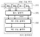
- FIG 3 illustrates a structure of a frequency multiplier including an edge combiner according to an embodiment of the present invention.
- the frequency multiplier includes an edge combiner including a delay locked loop 310, a pulse generator 320, a first signal output unit, and a second signal output unit. 330).
- the delay lock loop 310 includes a voltage control delay line having a plurality of delay cells and outputs a plurality of voltage control delay signals by sequentially delaying a predetermined input clock signal for a predetermined time.
- the pulse generator 320 receives each output signal of the voltage control delay line and generates a pulse signal.
- the edge combiner 330 generates a multiplied output signal through operations of the first signal output unit and the second signal output unit to be described in detail below.
- FIG. 4 is a flowchart illustrating a frequency multiplication method using an edge combiner according to an embodiment of the present invention.
- the frequency multiplication method using the edge combiner includes a voltage control delay signal output step (410); Pulse generation step 420; And generating a multiplied output signal including a first output signal generation step 431 and a second output signal generation step 432; It is made, including.
- the delay lock loop consists of a voltage controlled delay line (VCDL), a phase detector, a loop filter, and a charge pump (not shown).
- VCDL voltage controlled delay line
- phase detector phase detector
- loop filter loop filter
- charge pump charge pump
- the voltage control delay line delays and outputs the input clock of the delay lock loop by a predetermined time while passing through the delay cell.
- the phase detector compares the phase of the input clock of the delay locked loop and the output clock of the VCDL to generate a signal proportional to the phase difference.
- the charge pump converts the signal received from the phase detector into a specific voltage value and sends it to the loop filter.
- the loop filter converts the voltage sent from the charge pump into a constant control voltage and supplies it to the voltage control delay line.
- each delay cell of the voltage control delay line delays the input clock signal by a predetermined time unit and outputs the voltage control delay signal, respectively. For example, assuming four delay cells, four voltage control delay signals are output. Becomes
- the pulse generator generates a pulse in accordance with the rising edge of the output signal of the voltage control delay line.
- FIG. 5 is a circuit diagram illustrating a structure of an edge combiner according to an embodiment of the present invention.
- an edge combiner may include a first signal output unit 510 and a second signal output unit 520.
- the first signal output unit 510 includes an inverted signal output unit 512 including a plurality of NMOS transistors each receiving a 2n (n is an integer greater than or equal to 0) pulse signal to a gate terminal, and 2n + 1 (n is 0)
- the non-inverting signal output unit 511 may include a plurality of NMOS transistors, each of which receives the (th integer) th pulse signal as a gate terminal.
- the first signal output unit 510 includes a differential cascode voltage switch logic 515, and the first PMOS transistor and the second PMOS transistor of the differential cascode voltage switch logic 515 are turned off.
- the first control unit 513 and the second control unit 514 to control the operation to enable a high speed operation may be included.
- the first controller 513 may include a first inverter having an input connected to an output terminal of the non-inverting signal output unit, a first NMOS passgate and a first blocking PMOS transistor connected to the output terminal of the first inverter, respectively.
- the gate terminal of the first NMOS passgate and the first blocking PMOS transistor may be connected to an output terminal of the first inverter.
- the drain terminal of the first NMOS passgate and the first blocking PMOS transistor may be connected to the gate terminal of the first PMOS transistor.
- the second controller 514 may include a second inverter having an input connected to an output terminal of the inverted signal output unit, a second NMOS passgate and a second blocking PMOS transistor connected to an output terminal of the second inverter.
- the gate terminal of the second NMOS passgate and the second blocking PMOS transistor may be connected to an output terminal of the second inverter.
- the drain terminal of the second NMOS passgate and the second blocking PMOS transistor may be connected to the gate terminal of the second PMOS transistor.
- the second signal output unit 520 receives a third PMOS transistor that receives the output signal of the second inverter of the second control unit as a gate terminal and a third NMOS that receives the output signal of the first inverter of the first control unit as a gate terminal. It may include a transistor.
- FIG. 6 is a timing diagram illustrating an edge combiner operation according to an embodiment of the present invention.
- an initial signal condition of a node connecting the drain terminals of a plurality of NMOS transistors included in the inverted signal output unit 512 of the first signal output unit 510 is High and a non-inverted signal output.
- the initial signal condition of the node connecting the drain terminals of the plurality of NMOS transistors included in the unit may be a low state. That is, the inverted output signal ( Initial condition of) is High, non-inverted output signal ) May be in a low state.
- NMOS transistor on the inverted signal output unit 512 At the gate terminal of the ) Input, reverse output signal ( ) Is discharged to a low state.
- a signal input to the gate terminal of the first NMOS passgate ( ) May be in a high state.
- a first NMOS passgate having a source terminal connected to an output terminal of the inverted signal output unit 512 ( ) Operates so that the low signal is applied to the first PMOS transistor ( Is input to the gate terminal. At this time, the first PMOS transistor ( Input signal of the gate terminal of ) Becomes Low. First PMOS transistor ( ) And the node connecting the drain terminals of the plurality of NMOS transistors of the non-inverting signal output unit is charged and the output signal ( ) Becomes High.
- the first controller 513 for controlling the turn-off operation of the first PMOS transistor is operated.
- the first controller 513 uses the first PMOS transistor ( The process of controlling the turn-off operation of) will be described in detail with reference to FIG. 7.
- FIG. 7 is a circuit diagram illustrating a structure of a first control unit of an edge combiner according to an embodiment of the present invention.
- the first control unit includes a first inverter having an input connected to an output terminal of the non-inverting signal output unit, a first NMOS passgate and a first blocking PMOS transistor connected to the output terminal of the first inverter, respectively. can do.
- the first NMOS passgate () connected to the output terminal of The low signal is input to the gate terminal of the circuit and turned off.
- the first blocking PMOS transistor ( ) Receives the low signal to the gate terminal and turns it on.
- First blocking PMOS transistor ( ) Operates so that the first PMOS transistor ( Signal input to the gate terminal of ) To High. Thus, the first PMOS transistor ( Operation is turned off. At this time, the output signal of the first signal output unit ( ) Is in the High state.
- the node connecting the drain terminals of the plurality of NMOS transistors of the non-inverting signal output unit is charged, and the plurality of NMOS transistors ( The first PMOS transistor is turned off before the pulse signal is input to the gate terminal. Therefore, the size of the first PMOS transistor can be increased, the operation speed is increased, and there is no power loss due to the DC current generated at the switching moment.
- the increase of the junction capacitor at the output stage is smaller than that of the general edge combiner structure 2, it can operate at a higher speed.
- NMOS transistor on the inverted signal output side
- the NMOS transistor Pulse signal to the gate terminal of
- the node connecting the drain terminals of the plurality of NMOS transistors of the non-inverting signal output unit is discharged so that the non-inverting output signal ) Goes low.
- a first inverter connected to the output terminal of the non-inverting signal output unit ( ) Output signal goes high.
- a signal input to the gate terminal of the second NMOS passgate ( ) May be in a high state.
- a second NMOS passgate connected to an output terminal of the non-inverting signal output unit and a source terminal ( ) To operate the low signal to the second PMOS transistor ( Is input to the gate terminal. At this time, the second PMOS transistor ( Input signal of the gate terminal of ) Becomes Low. Second PMOS transistor ( ) And the node connecting the drain terminals of the plurality of NMOS transistors of the inverted signal output unit is charged and the inverted output signal ( ) Becomes High.
- the second control unit may include a second inverter having an input connected to an output terminal of the non-inverting signal output unit, a second NMOS passgate and a second blocking PMOS transistor connected to the output terminal of the second inverter, respectively.
- 2nd inverter The second NMOS passgate connected to the output terminal of The low signal is input to the gate terminal of the circuit and turned off.
- the second blocking PMOS transistor ( ) Operates by receiving Low signal to the gate terminal.
- Second blocking PMOS transistor Operates so that the second PMOS transistor ( Signal input to the gate terminal of ) To the High state and the second PMOS transistor ( Operation is turned off. At this time, the output signal of the first signal output unit ( ) Is in the High state.
- the NMOS transistor on the inverting signal output side Before the pulse signal is input to the gate terminal of the second PMOS transistor ( ) Is turned off. Therefore, the second PMOS transistor ( ) Can be increased, the operation speed is increased, and there is no power loss due to the DC current generated at the moment of switching.
- the size of the junction capacitor of the output stage is smaller, it can operate at a higher speed.
- the first signal output step 431 of the edge combiner operates while alternately repeating the inverted signal output unit and the non-inverted signal output unit.
- the operation of the first signal output step it is possible to have an improved operation speed compared to general edge combiner structures 1 and 2.
- the duty ratio of the signal appearing at the inverted signal output unit and the non-inverted signal output unit still does not maintain 50%. .
- the above problem is solved through the second signal output step.
- the second signal output unit may include a third PMOS transistor that receives the output signal of the second inverter of the second control unit as the gate terminal and a third NMOS transistor that receives the output signal of the first inverter of the first control unit as the gate terminal.
- the drain terminal of the third PMOS transistor and the drain terminal of the third NMOS transistor may be connected to each other.
- the initial signal condition of the node connecting the drain terminal of the third PMOS transistor and the drain terminal of the third NMOS transistor may be in a high state.
- Input signal of the gate terminal of the third PMOS transistor ( ) May be in a low state.
- Input signal of the gate terminal of the third NMOS transistor ( ) May be in a low state.
- the third PMOS transistor is an inverted output signal ( The output signal of the drain terminal is set to High for each rising edge. This is the inverted output signal ( ) Is inverted through the second inverter and input to the gate terminal of the third PMOS transistor.
- the third NMOS transistor is a non-inverting output signal ( The output signal of the drain terminal is set to Low for each rising edge. This is a non-inverted output signal ( ) Is inverted through the first inverter, inverted once again through an inverter connected to the gate terminal of the third NMOS transistor, and input to the gate terminal of the third NMOS transistor.
- the second signal output unit toggles a signal output by operating the third PMOS transistor and the third NMOS transistor for each rising edge of the non-inverted signal output unit and the inverted signal output unit output signals.
- the duty ratio can be 50%.
- FIG. 8 is a graph showing the operation speed of the edge combiner according to an embodiment of the present invention with respect to the multiplication ratio.
- a general edge combiner structure 1, a general edge combiner structure 2, and an edge combiner structure according to an embodiment of the present invention were modeled with a simple RC delay, and an elmore delay calculation method was used.
- the operating speed is expressed by normalizing the case of the multiplication ratio 1 of the general edge combiner structure 1.
- the operation speed is kept constant. This is because the signal generated by the first signal output part operates too fast to sufficiently turn on the third PMOS transistor and the third NMOS transistor of the second signal output part. Therefore, when the multiplication ratio is less than 4 times, the operating speed of the second signal output unit determines the operating speed of the entire edge combiner.
- the edge combiner structure according to an embodiment of the present invention has a speed of 2 to 2.5 times faster, which greatly increases the size of the first PMOS transistor and the second PMOS transistor. Because you can.
- the operation speed is slower than the general edge combiner structure 2, which is a control process for turning off the first PMOS transistor and the second PMOS transistor. This is due to the delay caused by.
- the delay is a fixed value irrespective of the multiplication ratio, and the increase rate of the junction capacitors at the output terminals of the inverted signal output unit and the non-inverted signal output unit is small compared to the general edge combiner structure 2, so that the multiplication ratio As it increases, it can have a faster operating speed.
- FIG. 9 is a graph showing the area of the edge combiner with respect to the multiplication ratio according to an embodiment of the present invention.
- the edge combiner since the first control unit and the second control unit are additionally configured in addition to the general edge combiner structure 1, the edge combiner always has a larger area than the general edge combiner structure 1.
- the area of the edge combiner according to an embodiment of the present invention was large. This is due to the addition of the first controller and the second controller.
- the area increase rate is smaller than that of the general edge combiner structure 2, and thus, the area increase rate is smaller when the multiplication rate is 6 times or more.
Landscapes
- Physics & Mathematics (AREA)
- Nonlinear Science (AREA)
- Pulse Circuits (AREA)
Abstract
본 발명은 에지컴바이너의 구조 및 이를 이용한 주파수 체배기, 주파수 체배방법에 관한 것이다. 본 발명의 일실시예에 따른 에지컴바이너는 NMOS 패스게이트, 인버터 및 차단 PMOS 트랜지스터로 구성되는 별도의 제어부를 이용하여 차동 캐스코드 전압 스위치 로직의 PMOS 트랜지스터의 턴오프(turn-off) 동작을 제어함으로써, 고속 동작이 가능하게 하여, 주파수 체배기의 성능을 향상시킬 수 있다.
Description
본 발명은 기본전자회로에 관한 것으로서, 보다 상세하게는 향상된 성능을 가지는 주파수 체배기 및 체배방법에 관한 것이다.
지연고정루프(Delay Locked Loop;DLL)는 전자 장치에서 내부 클럭을 발생시키기 위하여 이용된다. 일반적인 지연고정루프는 수신된 외부 클럭을 지연 라인을 이용하여 소정의 시간만큼 지연시켜서 외부 클럭에 동기된 내부 클럭을 발생한다.이러한 지연고정루프 기반의 클럭 발생기는 대부분의 위상고정루프 기반의 클럭 발생기 및 국부 발진기와 비교할 때 지터의 축적이 없어 위상 잡음이 적으며, 루프 필터의 구조가 간단하므로 소형화가 가능하다. 특히, 반도체 메모리 장치의 경우 외부 클럭의 주파수를 체배한 주파수를 갖는 내부 클럭을 이용함으로써 반도체 메모리 장치의 데이터 전송 속도를 증가시킬 수 있으며, 정확한 위상 지연 및 듀티 비를 갖는 클럭들을 데이터 전송에 이용함으로써 고속 데이터 전송시 에러를 줄일 수 있다.
한편, 지연고정루프의 이러한 장점을 이용한 주파수 체배기는 전압 제어 지연선이 지터를 축적하지 않고 각 동작 모드에서 다른 동작 모드로 전환할 때 빠르게 재 락킹되는 장점이 있다. 또한 지연고정루프 기반의 주파수 체배기는 1차 시스템으로 안정도를 유지할 수 있다.
이러한 주파수 체배기는 펄스 발생기, 에지컴바이너, 체배율 제어부로 구성되며, 특히 에지컴바이너는 실제로 체배된 신호를 만들어내는 부분이다. 따라서 에지컴바이너는 주파수 체배기의 성능 척도인 동작속도 및 듀티 비 등을 결정하는 가장 중요한 부분이라 할 수 있다.
이러한 에지컴바이너의 일반적인 구조들은 출력신호의 듀티 비가 50%가 되지 않는다는 점, PMOS 트랜지스터의 사이즈를 크게 할 수 없어 동작속도가 느리다는 점, 구현에 필요한 면적이 넓다는점 등의 문제가 있었다.
이에 본 발명이 이루고자 하는 기술적인 과제는 개선된 구조를 이용하여 향상된 성능을 갖는 에지컴바이너와 이를 이용한 주파수 체배기 및 체배방법을 제공하는 것이다.
본 발명에 따른 에지 컴바이너는 차동 캐스코드 전압 스위치 로직(Differential Cascode Voltage Switch Logic, DCVSL)을 포함하되, 상기 차동 캐스코드 전압 스위치 로직의 제1PMOS 트랜지스터 및 제2PMOS 트랜지스터의 턴오프(turn-off)동작을 각각 제어하여 고속 동작이 가능하도록 하는 제1제어부 및 제2제어부를 포함하는 제1신호출력부; 및 상기 제1신호출력부의 출력신호마다 토글링하여 신호의 듀티 비를 조절하는 것을 특징으로 하는 제2신호출력부; 를 포함한다.
상기 제1제어부는 상기 차동 캐스코드 전압 스위치 로직의 비반전신호 출력부의 출력단에 입력단이 연결되는 제1인버터; 상기 제1인버터의 출력단과 각각 연결되는 제1NMOS 패스게이트(passgate) 및 제1 차단 PMOS 트랜지스터를 포함하되, 상기 제1NMOS 패스게이트 및 제1차단 PMOS 트랜지스터의 드레인 단자는 상기 제1PMOS 트랜지스터에 연결되며, 상기 제2제어부는 상기 차동 캐스코드 전압 스위치 로직의 반전신호 출력부의 출력단에 입력단이 연결되는 제2인버터; 상기 제2인버터의 출력단과 각각 연결되는 제2NMOS 패스게이트(passgate) 및 제2 차단 PMOS 트랜지스터를 포함하되, 상기 제2NMOS 패스게이트 및 제2차단 PMOS 트랜지스터의 드레인 단자는 상기 제2PMOS 트랜지스터에 연결되는 것을 특징으로 한다. 상기 반전신호 출력부는 2n(n은 0이상의 정수) 번째 펄스신호를 게이트 단자로 각각 입력받는 복수의 NMOS 트랜지스터를 포함하고, 상기 비반전신호 출력부는 2n+1(n은 0이상의 정수) 번째 펄스신호를 게이트 단자로 각각 입력받는 복수의 NMOS 트랜지스터를 포함한다.
또한, 상기 제1제어부는 상기 비반전신호 출력부의 복수의 NMOS 트랜지스터의 드레인 단자를 연결한 노드가 충전되고, 상기 비반전신호 출력부의 복수의 NMOS 트랜지스터가 각각 2n+1(n은 0이상의 정수)번째 펄스 신호를 게이트 단자로 입력받기 전에 상기 제1PMOS 트랜지스터의 동작을 턴오프(turn-off) 시키며,
상기 제2제어부는 상기 반전신호 출력부의 복수의 NMOS 트랜지스터의 드레인 단자를 연결한 노드가 충전되고, 상기 반전신호 출력부의 복수의 NMOS 트랜지스터가 각각 2n(n은 1이상의 정수)번째 펄스 신호를 게이트 단자로 입력받기 전에 상기 제1PMOS 트랜지스터의 동작을 턴오프(turn-off) 시키는 것을 특징으로 한다.
한편, 상기 제2신호출력부는 상기 제2제어부의 제2인버터의 출력 신호를 게이트 단자로 입력받는 제3PMOS 트랜지스터; 및 상기 제1제어부의 제1인버터의 출력 신호를 게이트 단자로 입력받는 제3NMOS 트랜지스터; 를 포함하며, 상기 제1신호출력부의 출력신호마다 토글링하여 신호의 듀티 비를 50%로 하는 것을 특징으로 한다.
또한, 본 발명에 따른 에지컴바이너를 이용한 주파수 체배기는 복수 개의 지연셀을 가지는 전압제어지연선을 포함하며, 소정의 입력클럭신호를 소정시간 순차적으로 지연시켜 복수 개의 전압제어지연신호를 출력하는 지연 고정 루프; 상기 지연고정루프의 전압제어지연선의 각 출력신호를 입력받아 펄스를 생성하는 펄스 발생기; 및 차동 캐스코드 전압 스위치 로직(differential cascode voltage switch logic, DCVSL)을 포함하되, 상기 차동 캐스코드 전압 스위치 로직의 제1PMOS 트랜지스터 및 제2PMOS 트랜지스터의 턴오프(turn-off)동작을 제어하여 고속 동작이 가능하도록 하는 제1제어부 및 제2제어부를 포함하는 제1신호출력부와 상기 제1신호출력부의 출력신호마다 토글링하여 출력신호의 듀티 비를 50%로 하는 것을 특징으로 하는 제2신호출력부를 포함하는 에지컴바이너; 를 포함한다. 이때 상기 제1제어부는 상기 차동 캐스코드 전압 스위치 로직의 비반전신호 출력부의 출력단에 입력단이 연결되는 제1인버터; 상기 제1인버터의 출력단과 각각 연결되는 제1NMOS 패스게이트(passgate) 및 제1차단 PMOS 트랜지스터를 포함하되, 상기 제1NMOS 패스게이트 및 제1차단 PMOS 트랜지스터의 드레인 단자는 상기 제1PMOS 트랜지스터에 연결되며, 상기 제2제어부는 상기 차동 캐스코드 전압 스위치 로직의 반전신호 출력부의 출력단에 입력단이 연결되는 제2인버터; 상기 제2인버터의 출력단과 각각 연결되는 제2NMOS 패스게이트(passgate) 및 제2차단 PMOS 트랜지스터를 포함하되, 상기 제2NMOS 패스게이트 및 제2 차단 PMOS 트랜지스터의 드레인 단자는 상기 제2PMOS 트랜지스터에 연결되는 것을 특징으로 한다.
본 발명에 따른 에지컴바이너를 이용한 주파수 체배방법은 복수 개의 지연셀을 가지는 전압제어지연선을 포함하고, 소정의 입력클럭신호를 소정시간 지연시켜 복수 개의 전압제어지연신호를 출력하는 단계; 지연고정루프의 각 지연셀의 출력신호를 입력받아 펄스를 생성하는 단계; 및 상기 펄스를 이용하여 체배된 출력신호를 발생시키는 단계; 를 포함하되, 상기 체배된 출력신호를 발생시키는 단계는 제1제어부 및 제2제어부의 동작을 통해 차동 캐스코드 전압 스위치 로직의 제1PMOS 트랜지스터 및 제2PMOS 트랜지스터의 턴오프(turn-off)동작을 각각 제어하는 것을 특징으로 하는 제1출력신호 생성단계; 및 상기 제1출력신호 생성단계의 출력신호마다 토글링(toggling)하여 출력신호의 듀티 비를 50%로 하는 제2출력신호 생성단계; 를 더 포함하는 것을 특징으로 한다.
본 발명의 일실시예에 따른 에지컴바이너는 별도의 제어부를 통해 차동 캐스코드 전압 스위치 로직의 PMOS 트랜지스터의 턴오프(turn-off) 동작을 제어함으로써 고속 동작이 가능하다. 또한 출력신호의 듀티 비를 50%로 할 수 있으며, 적은 면적으로도 구현가능하다.
도 1은 일반적인 에지컴바이너의 구조1 을 나타낸 회로도이다.
도 2는 일반적인 에지컴바이너의 구조2 를 나타낸 회로도이다.
도 3은 본 발명의 일실시예에 따른 에지컴바이너를 포함하는 주파수 체배기의 구조를 나타낸 것이다.
도 4는 본 발명의 일실시예에 따른 에지컴바이너를 이용한 주파수 체배방법을 나타낸 흐름도이다.
도 5는 본 발명의 일실시예에 따른 에지컴바이너의 구조를 나타낸 회로도이다.
도 6은 본 발명의 일실시예에 따른 에지컴바이너 동작시의 타이밍 다이어그램을 나타낸 것이다.
도 7은 본 발명의 일실시예에 따른 에지컴바이너의 제1제어부의 구조를 나타낸 회로도이다.
도 8은 본 발명의 일실시예에 따른 에지컴바이너의 동작속도를 체배율에 대하여 나타낸 그래프이다.
도 9는 본 발명의 일실시예에 따른 에지컴바이너의 면적을 체배율에 대하여 나타낸 그래프이다.
실시예들은 여러 가지 다른 형태들로 구체화되어질 수 있고, 여기에서 설명되는 양태들로 한정되는 것으로 해석되지 않는다. 오히려, 상기 양태들은 실시예들을 더욱 철저하고 완전하게 되도록 해주며, 당업자에게 실시예들의 영역을 충분히 전달할 수 있도록 해준다.
또한, 명세서 전체에서, 어떤 부분이 어떤 구성요소를 "포함"한다고 할 때, 이는 특별히 반대되는 기재가 없는 한 다른 구성요소를 제외하는 것이 아니라 다른 구성요소를 더 포함할 수 있는 것을 의미한다.
도 1은 일반적인 에지컴바이너의 구조1을 나타낸 것이다.
도 1에 도시된 에지컴바이너 구조1의 동작은 다음과 같다. 차동 캐스코드 전압 스위치 로직(Differential Cascode Voltage Switch Logic;DCVSL) 구조의 에지컴바이너로서, 반전출력신호 ( )는 High, 비반전출력신호 (
 )는 Low 상태에서 반전신호 출력부 측 NMOS 트랜지스터(
 )의 게이트 단자에 펄스신호가 입력되면 반전신호 출력부 측 복수의 NMOS 트랜지스터의 드레인 단자를 연결한 노드가 방전되어 반전출력신호(
 )가 Low 상태가 된다. 반전신호 출력부의 출력단과 연결된 PMOS 트랜지스터(
 )가 동작(turn-on)하면서 비반전신호 출력부 측 복수의 NMOS 트랜지스터의 드레인 단자를 연결한 노드가 충전되어 비비반전 출력신호(
 )가 High 상태가 된다.
반전신호 출력부 측 NMOS 트랜지스터( )가 턴오프(turn-off) 되면, 비반전신호 출력부 측 NMOS 트랜지스터(
 )의 게이트 단자에 펄스신호가 입력된다. 비반전신호 출력부 측 복수의 NMOS 트랜지스터의 드레인 단자를 연결한 노드가 방전되어 비반전 출력신호(
 )가 Low 상태가 되면, 비반전신호 출력부의 출력단과 연결된 PMOS 트랜지스터(
 )가 동작하면서 반전출력신호(
 )가 High 상태가 된다. 상기의 동작이 반복적으로 수행되며, 이로써 체배된 1 싸이클의 파형이 발생된다.
그러나 이러한 일반적인 에지컴바이너 구조1의 경우, NMOS 트랜지스터( )가 동작(turn-on)되는 순간, 같은 노드에 연결되어 있는 PMOS 트랜지스터(
 )가 동작(turn-on)되어있는 상태이기 때문에, NMOS 트랜지스터(
 )가 노드를 방전시키기 위해서는 PMOS 트랜지스터(
 )의 구동능력(driving strength)이 NMOS 트랜지스터(
 )에 비해 절반 이상 작아야 한다. 따라서, 상승 에지를 발생시키는 속도가 느려지게 되고, 전체 에지컴바이너의 동작 속도 역시 느려지게 된다. 또한 상승 에지와 하강 에지의 발생 속도 차이가 크기 때문에 듀티 비가 깨어지며, 스위칭 순간에 발생하는 DC 전류에 의한 전력 손실이 발생하는 문제점이 있었다.
도 2는 일반적인 에지컴바이너의 구조2를 나타낸 것이다.
도 2에 도시된 일반적인 에지컴바이너의 구조2의 동작은 다음과 같다. CMOS 구조의 에지컴바이너로서, 반전출력신호( )가 High 인 상태에서 NMOS 트랜지스터(
 ) 에 펄스신호가 입력되어 동작(turn-on)하면, 반전출력신호(
 )가 Low 상태가 된다. 이어서 PMOS 트랜지스터(
 )가 동작하면 반전출력신호(
 )가 다시 High 상태가 된다. 이와 같은 동작이 반복되면서 체배된 신호를 발생시킨다.
하지만 이경우, PMOS 트랜지스터의 사용량이 많아져, 체배율이 증가할수록 PMOS 트랜지스터와 NMOS 트랜지스터의 드레인 단자를 연결한 노드에 형성되는 접합 커패시터가 빠르게 증가하여 생성할 수 있는 최대 주파수 크기가 급격히 감소한다는 문제가 있었다. 또한, PMOS 트랜지스터가 NMOS 트랜지스터와 구동능력이 같아지려면, 2.5 내지 3배의 크기가 필요하므로 면적이 크게 증가하는 문제점이 있었다.
이하에서 상술한 문제점을 해결하기 위한, 본 발명의 일실시예에 따른 에지컴바이너 및 이를 이용한 주파수 체배기, 주파수 체배방법에 대하여 도면을 참조하여 상세히 설명한다.
도 3은 본 발명의 일실시예에 따른 에지컴바이너를 포함하는 주파수 체배기의 구조를 나타낸 것이다.
도 3에 도시된 바와 같이, 본 발명의 일실시예에 따른 주파수 체배기는 지연고정루프(310), 펄스발생기(320), 제1신호출력부 및 제2신호출력부로 구성되는 에지컴바이너(330)를 포함할 수 있다.
지연고정루프(310)는 복수 개의 지연셀을 가지는 전압제어지연선을 포함하며, 소정의 입력 클럭신호를 소정시간 순차적으로 지연시켜 복수 개의 전압제어지연신호를 출력한다. 펄스발생기(320)는 전압제어지연선의 각 출력신호를 입력받아 펄스신호를 생성한다. 에지컴바이너(330)는 이하에서 상세히 설명할 제1신호출력부 및 제2신호출력부의 동작을 통해 체배된 출력신호를 생성한다.
도 4는 본 발명의 일실시예에 따른 에지컴바이너를 이용한 주파수 체배방법을 나타낸 흐름도이다.
도 4에 도시된 바와 같이, 본 발명의 일실시예에 따른 에지컴바이너를 이용한 주파수 체배방법은 전압제어지연신호 출력단계(410); 펄스 생성단계(420); 및 제1출력신호 생성단계(431) 및 제2출력신호 생성단계(432)를 포함하는 체배된 출력신호를 발생시키는 단계(430); 를 포함하여 이루어진다.
이하에서 전압제어지연신호 출력단계(410) 및 펄스 생성단계(420)에 대하여 상세히 설명한다.
지연고정루프는 전압제어지연선(Voltage Controlled Delay Line;VCDL), 위상검출기, 루프 필터, 전하펌프로 구성된다.(미도시)
전압제어지연선은 지연고정루프의 입력 클럭을 지연셀을 통과시키면서 소정시간만큼 지연시켜 출력한다. 위상검출기는 지연고정루프의 입력 클럭과 VCDL의 출력 클럭의 위상을 비교하여 위상차에 비례하는 신호를 발생시킨다. 전하펌프는 위상검출기에서 받은 신호를 특정한 전압 값으로 바꾼 뒤 루프 필터로 보낸다. 루프 필터는 전하펌프에서 보내진 전압을 일정한 제어전압으로 만들어 전압제어지연선에 공급한다.
즉, 전압제어지연선의 각 지연셀은 입력 클럭신호를 소정 시간단위로 지연시켜 각각 전압제어지연신호를 출력한다. 예를 들어, 지연셀을 4개로 가정하면 4개의 전압제어지연신호를 출력하며, 각 신호간 간격은  가 된다.
가 된다.
펄스발생기는 전압제어지연선의 출력신호의 상승 에지에 맞추어 펄스를 생성한다.
이하에서 제1출력신호 생성단계(431)에 대하여 상세히 설명한다.
도 5는 본 발명의 일실시예에 따른 에지컴바이너의 구조를 나타낸 회로도이다.
도 5에 도시된 바와 같이, 본 발명의 일실시예에 따른 에지컴바이너는 제1신호출력부(510)와 제2신호출력부(520)를 포함할 수 있다.
상기 제1신호출력부(510)는 2n(n은 0이상의 정수) 번째 펄스신호를 게이트 단자로 각각 입력받는 복수의 NMOS 트랜지스터를 포함하는 반전신호 출력부(512), 2n+1(n은 0이상의 정수) 번째 펄스신호를 게이트 단자로 각각 입력받는 복수의 NMOS 트랜지스터를 포함하는 비반전신호 출력부(511)를 포함할 수 있다.
또한, 상기 제1신호출력부(510)는 차동 캐스코드 전압 스위치 로직(515)을 포함하되, 상기 차동 캐스코드 전압 스위치 로직(515)의 제1PMOS 트랜지스터 및 제2PMOS 트랜지스터의 턴오프(turn-off)동작을 제어하여 고속 동작이 가능하도록 하는 제1제어부(513) 및 제2제어부(514)를 포함할 수 있다.
상기 제1제어부(513)는 비반전신호 출력부의 출력단에 입력단이 연결되는 제1인버터와, 상기 제1인버터의 출력단과 각각 연결되는 제1NMOS 패스게이트 및 제1 차단 PMOS 트랜지스터를 포함할 수 있다. 상기 제1NMOS 패스게이트 및 제1 차단 PMOS 트랜지스터의 게이트 단자는 상기 제1인버터의 출력단과 연결될 수 있다. 상기 제1NMOS 패스게이트 및 제1 차단 PMOS 트랜지스터의 드레인 단자는 제1PMOS 트랜지스터의 게이트 단자와 연결될 수 있다.
상기 제2제어부(514)는 반전신호 출력부의 출력단에 입력단이 연결되는 제2인버터와, 상기 제2인버터의 출력단과 연결되는 제2NMOS 패스게이트 및 제2 차단 PMOS 트랜지스터를 포함할 수 있다. 상기 제2NMOS 패스게이트 및 제2 차단 PMOS 트랜지스터의 게이트 단자는 상기 제2인버터의 출력단과 연결될 수 있다. 상기 제2NMOS 패스게이트 및 제2 차단 PMOS 트랜지스터의 드레인 단자는 제2PMOS 트랜지스터의 게이트 단자와 연결될 수 있다.
상기 제2신호출력부(520)는 상기 제2제어부의 제2인버터의 출력 신호를 게이트 단자로 입력받는 제3PMOS 트랜지스터와 상기 제1제어부의 제1인버터의 출력 신호를 게이트 단자로 입력받는 제3NMOS 트랜지스터를 포함할 수 있다.
이하에서 제1신호출력부(510)의 동작에 대하여 제1제어부(513) 및 제2제어부(514)의 동작을 포함하여 상세히 설명한다.
도 6은 본 발명의 일실시예에 따른 에지컴바이너 동작시의 타이밍 다이어그램을 나타낸 것이다.
도 6에 도시된 바와 같이, 상기 제1신호출력부(510)의 반전신호 출력부(512)에 포함된 복수의 NMOS 트랜지스터들의 드레인 단자를 연결한 노드의 초기신호조건은 High, 비반전신호 출력부에 포함된 복수의 NMOS 트랜지스터들의 드레인 단자를 연결한 노드의 초기신호조건은 Low 상태일 수 있다. 즉, 반전출력신호 ( )의 초기조건은 High, 비반전출력신호 (
 )의 초기조건은 Low 상태일 수 있다.
반전신호 출력부(512) 측 NMOS 트랜지스터( )의 게이트 단자에 펄스신호(
 )가 입력되면 반전출력신호 (
 )가 방전되어 Low 상태가 된다. 반전신호 출력부(512)의 출력단에 입력단이 연결된 제2인버터(
 )의 출력신호는 High 상태가 된다. 제1NMOS 패스게이트의 게이트 단자로 입력되는 신호(
 )의 초기조건은 High 상태일 수 있다.
반전신호 출력부(512)의 출력단자에 소오스 단자가 연결된 제1 NMOS 패스게이트( )가 동작하여 Low 신호가 제1PMOS 트랜지스터(
 )의 게이트 단자로 입력된다. 이때, 제1PMOS 트랜지스터(
 )의 게이트 단자의 입력신호(
 )는 Low 상태가 된다. 제1PMOS 트랜지스터(
 )가 동작하고, 비반전신호 출력부의 복수의 NMOS 트랜지스터의 드레인 단자를 연결한 노드가 충전되어 출력신호 (
 )가 High 상태가 된다. 다음으로 기존의 에지컴바이너 구조1과 달리, 제1PMOS 트랜지스터의 턴오프(turn-off) 동작을 제어하기 위한 제1제어부(513)가 동작한다.
이하에서는 제1제어부(513)가 제1PMOS 트랜지스터( )의 턴오프(turn-off) 동작을 제어하는 과정에 대하여 도 7을 참조하여 상세히 설명한다.
도 7은 본 발명의 일실시예에 따른 에지컴바이너의 제1제어부의 구조를 나타낸 회로도이다.
도 7에 도시된 바와 같이, 제1제어부는 비반전신호 출력부의 출력단에 입력단이 연결되는 제1인버터와, 상기 제1인버터의 출력단과 각각 연결되는 제1NMOS 패스게이트 및 제1 차단 PMOS 트랜지스터를 포함할 수 있다.
상기 제1제어부의 동작을 상세히 설명하면 다음과 같다. 비반전신호 출력부의 출력단에 입력단이 연결된 제1인버터( )의 출력신호는 Low 상태가 된다. 제1인버터(
 )의 출력단에 연결된 제1NMOS 패스게이트(
 )의 게이트 단자로 Low 신호가 입력되어 턴오프(turn-off) 된다. 반면, 제1 차단 PMOS 트랜지스터(
 )는 게이트 단자로 Low 신호를 입력받아 동작(turn-on)한다. 제1 차단 PMOS 트랜지스터(
 )가 동작하여 제1PMOS 트랜지스터(
 )의 게이트 단자로 입력되는 신호(
 )를 High 상태로 한다. 이로써, 제1PMOS 트랜지스터(
 )의 동작이 턴오프(turn-off)된다. 이때, 제1신호출력부의 출력신호(
 )는 High 상태이다.
일반적인 에지컴바이너 구조1과 달리 비반전신호 출력부의 복수의 NMOS 트랜지스터의 드레인 단자를 연결한 노드가 충전되고, 상기 비반전신호 출력부 측 복수의 NMOS 트랜지스터( )의 게이트 단자로 펄스신호가 입력되기 전에 제1PMOS 트랜지스터가 턴오프(turn-off)된다. 따라서, 제1PMOS 트랜지스터의 크기를 크게 할 수 있어, 동작속도가 빨라지고, 스위칭 순간에 발생하는 DC 전류에 의한 전력 손실이 없다.
또한, 일반적인 에지컴바이너 구조2에 비해 출력단의 접합 커패시터의 증가가 더 작기 때문에 보다 빠른 속도로 동작할 수 있다.
계속해서 제1신호출력단계(431)에 대하여 상세히 설명한다.
반전신호 출력부 측 NMOS 트랜지스터( )가 턴오프(turn-off)되면, 비반전신호 출력부 측 NMOS 트랜지스터(
 )의 게이트 단자로 펄스신호(
 )가 입력된다. 비반전신호 출력부의 복수의 NMOS 트랜지스터의 드레인 단자를 연결한 노드가 방전되어 비반전출력신호 (
 )가 Low 상태가 된다. 비반전신호 출력부의 출력단에 입력단이 연결된 제1인버터(
 )의 출력신호는 High 상태가 된다. 제2NMOS 패스게이트의 게이트 단자로 입력되는 신호(
 )의 초기조건은 High 상태일 수 있다.
비반전신호 출력부의 출력단과 소오스 단자가 연결된 제2 NMOS 패스게이트( )가 동작하여 Low 신호가 제2PMOS 트랜지스터(
 )의 게이트 단자로 입력된다. 이때, 제2PMOS 트랜지스터(
 )의 게이트 단자의 입력신호(
 )는 Low 상태가 된다. 제2PMOS 트랜지스터(
 )가 동작하고, 반전신호 출력부의 복수의 NMOS 트랜지스터의 드레인 단자를 연결한 노드가 충전되어 반전출력신호 (
 )가 High 상태가 된다.
이하에서는 제2제어부가 제2PMOS 트랜지스터의 턴오프(turn-off) 동작을 제어하는 과정에 대해 상세히 설명한다.
제2제어부는 비반전신호 출력부의 출력단에 입력단이 연결되는 제2인버터와, 상기 제2인버터의 출력단과 각각 연결되는 제2NMOS 패스게이트 및 제2차단 PMOS 트랜지스터를 포함할 수 있다.
상기 제2제어부의 동작을 상세히 설명하면 다음과 같다. 반전신호 출력부의 출력단에 입력단이 연결된 제2인버터( )의 출력신호는 Low 상태가 된다. 제2인버터(
 )의 출력단에 연결된 제2NMOS 패스게이트(
 )의 게이트 단자로 Low 신호가 입력되어 턴오프(turn-off) 된다. 반면, 제2차단 PMOS 트랜지스터(
 )는 게이트 단자로 Low 신호를 입력받아 동작한다. 제2차단 PMOS 트랜지스터(
 )가 동작하여 제2PMOS 트랜지스터(
 )의 게이트 단자로 입력되는 신호(
 )를 High 상태로 하고, 제2PMOS 트랜지스터(
 )의 동작이 턴오프(turn-off)된다. 이때, 제1신호출력부의 출력신호(
 )는 High 상태이다.
일반적인 에지컴바이너 구조1과는 달리 반전신호 출력부 측 NMOS 트랜지스터( )의 게이트 단자로 펄스신호가 입력되기 전에 제2PMOS 트랜지스터(
 )가 턴오프(turn-off)된다. 따라서, 제2PMOS 트랜지스터(
 )의 크기를 크게 할 수 있어, 동작속도가 빨라지고, 스위칭 순간에 발생하는 DC 전류에 의한 전력 손실이 없다.
또한, 일반적인 에지컴바이너 구조2와 달리 출력단의 접합 커패시터의 크기가 더 작기 때문에 보다 빠른 속도로 동작할 수 있다.
상기와 같은 반전신호 출력부 및 비반전신호 출력부 측 동작을 교대로 반복하면서 에지컴바이너의 제1신호출력단계(431)가 동작한다.
상기의 제1신호출력단계의 동작을 통해 일반적인 에지컴바이너 구조1 및 구조2에 비해 향상된 동작속도를 가지는 것이 가능하다. 하지만, 출력신호의 상승에지가 생성되는 속도와 하강에지가 생성되는 속도의 차이는 여전히 존재하기 때문에, 반전신호 출력부 및 비반전신호 출력부에서 나타나는 신호의 듀티 비는 여전히 50%를 유지하지 못한다. 이에 본 발명의 일실시예에 따른 에지컴바이너의 구조에서는 제2신호출력단계를 통해 상기의 문제점을 해결하고 있다.
이하에서 제2신호출력단계(432)에 대하여 상세히 설명한다.
제2신호출력부는 제2제어부의 제2인버터의 출력 신호를 게이트 단자로 입력받는 제3PMOS 트랜지스터와 제1제어부의 제1인버터의 출력 신호를 게이트 단자로 입력 받는 제3NMOS 트랜지스터를 포함할 수 있다. 상기 제3PMOS 트랜지스터의 드레인 단자와 상기 제3NMOS 트랜지스터의 드레인 단자는 서로 연결되는 것을 특징으로 한다. 또한, 상기 제3PMOS 트랜지스터의 드레인 단자와 상기 제3NMOS 트랜지스터의 드레인 단자를 연결한 노드의 초기신호조건은 High 상태일 수 있다. 상기 제3PMOS 트랜지스터의 게이트 단자의 입력신호( )의 초기조건은 Low 상태일 수 있다. 상기 제3NMOS 트랜지스터의 게이트 단자의 입력신호(
 )의 초기조건은 Low 상태일 수 있다.
상기 제3PMOS 트랜지스터는 반전출력신호( )의 상승에지마다 드레인 단자의 출력신호를 High 상태로 한다. 이는 반전출력신호(
 )가 제2인버터를 통해 반전되어 상기 제3PMOS 트랜지스터의 게이트 단자로 입력되기 때문이다.
상기 제3NMOS 트랜지스터는 비반전출력신호( )의 상승에지마다 드레인 단자의 출력신호를 Low 상태로 한다. 이는 비반전출력신호(
 )가 제1인버터를 통해 반전되고, 상기 제3NMOS 트랜지스터의 게이트 단자와 연결된 인버터를 통해 다시 한번 반전되어 상기 제3NMOS 트랜지스터의 게이트 단자로 입력되기 때문이다.
즉, 제2신호출력부는 제1신호출력부의 비반전신호 출력부 및 반전신호 출력부의 출력신호의 상승에지마다 각각 상기 제3PMOS 트랜지스터와 상기 제3NMOS 트랜지스터가 동작하여 출력한 신호를 토글링(toggling) 하고, 반전시켜 출력함으로써, 출력신호( )의 듀티 비를 50%로 할 수 있다.
도 8는 본 발명의 일실시예에 따른 에지컴바이너의 동작속도를 체배율에 대하여 나타낸 그래프이다.
일반적인 에지컴바이너 구조1, 일반적인 에지컴바이너 구조2 및 본 발명의 일실시예에 따른 에지컴바이너의 구조를 간단한 RC delay로 모델링 하고, elmore delay 계산 방법을 사용하였다. 동작속도는 일반적인 에지컴바이너 구조1의 체배율 1인 경우를 기준으로 정규화하여 표현하였다.
본 발명의 일실시예에 따른 에지컴바이너의 구조에서는 체배율이 4배 미만일 경우, 동작 속도가 일정하게 유지된다. 이는 제1신호출력부에서 만들어 낸 신호가 너무 빠르게 동작하여 제2신호출력부의 제3PMOS 트랜지스터 및 제3NMOS 트랜지스터를 충분히 동작(turn-on) 시키지 못하기 때문이다. 따라서, 체배율 4배 미만에서는 제2신호출력부의 동작속도가 전체 에지컴바이너의 동작속도를 결정하게 된다.
일반적인 에지컴바이너 구조1과 비교했을 때, 본 발명의 일실시예에 따른 에지컴바이너 구조는 2배 내지 2.5배 빠른 동작속도를 가졌으며, 이는 제1PMOS 트랜지스터 및 제2PMOS 트랜지스터의 크기를 크게 할 수 있기 때문이다. 한편, 체배율이 4배 미만의 작은 값을 가지는 경우, 일반적인 에지컴바이너 구조2에 비해 동작속도가 느리게 되는데, 이는 제1PMOS 트랜지스터 및 제2PMOS 트랜지스터를 턴오프(turn-off) 시키기 위한 제어과정에 의해 생기는 delay 때문이다. 하지만, 상기 delay는 체배율에 상관없이 고정되어 있는 값이며, 반전신호 출력부 및 비반전신호 출력부의 출력단의 접합 커패시터가 증가되는 정도는 일반적인 에지컴바이너 구조2에 비해 작기 때문에, 체배율이 증가할수록 더 빠른 동작속도를 가질 수 있다.
도 9은 본 발명의 일실시예에 따른 에지컴바이너의 면적을 체배율에 대하여 나타낸 그래프이다.
면적의 경우, 체배율이 증가할수록 펄스를 입력받는 NMOS 트랜지스터 수가 많아져 일반적으로 면적이 증가하였다.
본 발명의 일실시예에 따른 에지컴바이너는 일반적인 에지컴바이너 구조1에 제1제어부 및 제2제어부를 추가적으로 구성하였으므로, 일반적인 에지컴바이너 구조1에 비해 항상 면적이 크게 나타났다.
또한, 일반적인 에지컴바이너 구조2와 비교시에도 체배율이 6배 미만인 경우, 본 발명의 일실시예에 따른 에지컴바이너의 면적이 크게 나타났다. 이는 제1제어부 및 제2제어부의 추가 때문이다. 하지만, 체배율이 증가함에 따른 면적 증가율은 일반적인 에지컴바이너 구조2에 비해 작기 때문에, 체배율이 6배 이상인 경우에는 면적이 더 작게 나타났다.
본 발명의 권리범위는 상술한 실시 예에 한정되는 것이 아니라 첨부된 특허청구범위 내에서 다양한 형태의 실시예로 구현될 수 있다. 특허청구범위에서 청구하는 본 발명의 요지를 벗어남이 없이 당해 발명이 속하는 기술 분야에서 통상의 지식을 가진 자라면 누구든지 변형 가능한 다양한 범위까지 본 발명의 청구범위 기재의 범위 내에 있는 것으로 본다.
Claims (9)
- 펄스 발생기로부터 생성된 펄스를 이용하여 상승 에지 및 하강 에지를 생성하는 에지컴바이너에 있어서,차동 캐스코드 전압 스위치 로직(Differential Cascode Voltage Switch Logic, DCVSL)을 포함하되, 상기 차동 캐스코드 전압 스위치 로직의 제1PMOS 트랜지스터 및 제2PMOS 트랜지스터의 턴오프(turn-off)동작을 각각 제어하여 고속 동작이 가능하도록 하는 제1제어부 및 제2제어부를 포함하는 제1신호출력부; 및상기 제1신호출력부의 출력신호마다 토글링하여 신호의 듀티 비를 조절하는 것을 특징으로 하는 제2신호출력부; 를 포함하는 에지컴바이너.
- 제 1 항에 있어서,상기 제1제어부는 상기 차동 캐스코드 전압 스위치 로직의 비반전신호 출력부의 출력단에 입력단이 연결되는 제1인버터;상기 제1인버터의 출력단과 각각 연결되는 제1NMOS 패스게이트(passgate) 및제1 차단 PMOS 트랜지스터를 포함하되,상기 제1NMOS 패스게이트 및 제1차단 PMOS 트랜지스터의 드레인 단자는 상기 제1PMOS 트랜지스터에 연결되며,상기 제2제어부는 상기 차동 캐스코드 전압 스위치 로직의 반전신호 출력부의 출력단에 입력단이 연결되는 제2인버터;상기 제2인버터의 출력단과 각각 연결되는 제2NMOS 패스게이트(passgate) 및제2 차단 PMOS 트랜지스터를 포함하되,상기 제2NMOS 패스게이트 및 제2차단 PMOS 트랜지스터의 드레인 단자는 상기 제2PMOS 트랜지스터에 연결되는 것을 특징으로 하는 에지컴바이너.
- 제 2 항에 있어서,상기 반전신호 출력부는 2n(n은 0이상의 정수) 번째 펄스신호를 게이트 단자로 각각 입력받는 복수의 NMOS 트랜지스터를 포함하고, 상기 비반전신호 출력부는 2n+1(n은 0이상의 정수) 번째 펄스신호를 게이트 단자로 각각 입력받는 복수의 NMOS 트랜지스터를 포함하는 것을 특징으로 하는 에지컴바이너.
- 제 3 항에 있어서,상기 제1제어부는 상기 비반전신호 출력부의 복수의 NMOS 트랜지스터의 드레인 단자를 연결한 노드가 충전되고, 상기 비반전신호 출력부의 복수의 NMOS 트랜지스터가 각각 2n+1(n은 0이상의 정수)번째 펄스 신호를 게이트 단자로 입력받기 전에 상기 제1PMOS 트랜지스터의 동작을 턴오프(turn-off) 시키며,상기 제2제어부는 상기 반전신호 출력부의 복수의 NMOS 트랜지스터의 드레인 단자를 연결한 노드가 충전되고, 상기 반전신호 출력부의 복수의 NMOS 트랜지스터가 각각 2n(n은 1이상의 정수)번째 펄스 신호를 게이트 단자로 입력받기 전에 상기 제1PMOS 트랜지스터의 동작을 턴오프(turn-off) 시키는 것을 특징으로 에지컴바이너.
- 제 1 항에 있어서, 상기 제2신호출력부는상기 제2제어부의 제2인버터의 출력 신호를 게이트 단자로 입력받는 제3PMOS 트랜지스터; 및상기 제1제어부의 제1인버터의 출력 신호를 게이트 단자로 입력받는 제3NMOS 트랜지스터; 를 포함하는 에지컴바이너.
- 제 5 항에 있어서,상기 제2신호출력부는 상기 제1신호출력부의 출력신호마다 토글링하여 신호의 듀티 비를 50%로 하는 것을 특징으로 하는 에지컴바이너.
- 복수 개의 지연셀을 가지는 전압제어지연선을 포함하며, 소정의 입력클럭신호를 소정시간 순차적으로 지연시켜 복수 개의 전압제어지연신호를 출력하는 지연 고정 루프;상기 지연고정루프의 전압제어지연선의 각 출력신호를 입력받아 펄스를 생성하는 펄스 발생기; 및차동 캐스코드 전압 스위치 로직(differential cascode voltage switch logic, DCVSL)을 포함하되, 상기 차동 캐스코드 전압 스위치 로직의 제1PMOS 트랜지스터 및 제2PMOS 트랜지스터의 턴오프(turn-off)동작을 제어하여 고속 동작이 가능하도록 하는 제1제어부 및 제2제어부를 포함하는 제1신호출력부와 상기 제1신호출력부의 출력신호마다 토글링하여 출력신호의 듀티 비를 50%로 하는 것을 특징으로 하는 제2신호출력부를 포함하는 에지컴바이너;를 포함하는 주파수 체배기.
- 제 7 항에 있어서,상기 제1제어부는 상기 차동 캐스코드 전압 스위치 로직의 비반전신호 출력부의 출력단에 입력단이 연결되는 제1인버터;상기 제1인버터의 출력단과 각각 연결되는 제1NMOS 패스게이트(passgate) 및제1차단 PMOS 트랜지스터를 포함하되,상기 제1NMOS 패스게이트 및 제1차단 PMOS 트랜지스터의 드레인 단자는 상기 제1PMOS 트랜지스터에 연결되며,상기 제2제어부는 상기 차동 캐스코드 전압 스위치 로직의 반전신호 출력부의 출력단에 입력단이 연결되는 제2인버터;상기 제2인버터의 출력단과 각각 연결되는 제2NMOS 패스게이트(passgate) 및제2차단 PMOS 트랜지스터를 포함하되,상기 제2NMOS 패스게이트 및 제2 차단 PMOS 트랜지스터의 드레인 단자는 상기 제2PMOS 트랜지스터에 연결되는 것을 특징으로 주파수 체배기.
- 복수 개의 지연셀을 가지는 전압제어지연선을 포함하고, 소정의 입력클럭신호를 소정시간 지연시켜 복수 개의 전압제어지연신호를 출력하는 단계;지연고정루프의 각 지연셀의 출력신호를 입력받아 펄스를 생성하는 단계; 및상기 펄스를 이용하여 체배된 출력신호를 발생시키는 단계; 를 포함하되,상기 체배된 출력신호를 발생시키는 단계는 제1제어부 및 제2제어부의 동작을 통해 차동 캐스코드 전압 스위치 로직의 제1PMOS 트랜지스터 및 제2PMOS 트랜지스터의 턴오프(turn-off)동작을 각각 제어하는 것을 특징으로 하는 제1출력신호 생성단계; 및상기 제1출력신호 생성단계의 출력신호마다 토글링(toggling)하여 출력신호의 듀티 비를 50%로 하는 제2출력신호 생성단계; 를 더 포함하는 것을 특징으로 하는 주파수 체배방법.
Applications Claiming Priority (2)
| Application Number | Priority Date | Filing Date | Title |
|---|---|---|---|
| KR10-2011-0011142 | 2011-02-08 | ||
| KR1020110011142A KR101208026B1 (ko) | 2011-02-08 | 2011-02-08 | 에지컴바이너, 이를 이용한 주파수 체배기 및 주파수 체배방법 |
Publications (1)
| Publication Number | Publication Date |
|---|---|
| WO2012108576A1 true WO2012108576A1 (ko) | 2012-08-16 |
Family
ID=46638780
Family Applications (1)
| Application Number | Title | Priority Date | Filing Date |
|---|---|---|---|
| PCT/KR2011/002001 Ceased WO2012108576A1 (ko) | 2011-02-08 | 2011-03-23 | 에지컴바이너, 이를 이용한 주파수 체배기 및 주파수 체배방법 |
Country Status (2)
| Country | Link |
|---|---|
| KR (1) | KR101208026B1 (ko) |
| WO (1) | WO2012108576A1 (ko) |
Families Citing this family (2)
| Publication number | Priority date | Publication date | Assignee | Title |
|---|---|---|---|---|
| KR102024435B1 (ko) | 2017-11-30 | 2019-09-23 | 연세대학교 산학협력단 | Dll 기반의 주파수 체배기를 위한 에지결합장치 및 그 방법 |
| KR102718725B1 (ko) * | 2024-02-26 | 2024-10-17 | 주식회사 아크칩스 | 위상고정루프를 포함하고, 기준입력신호의 주파수를 제어하여 정수경계스퍼를 회피할 수 있는 장치 |
Citations (4)
| Publication number | Priority date | Publication date | Assignee | Title |
|---|---|---|---|---|
| KR100641360B1 (ko) * | 2004-11-08 | 2006-11-01 | 삼성전자주식회사 | 지연 동기 루프 및 이를 구비한 반도체 메모리 장치 |
| KR20070071142A (ko) * | 2005-12-29 | 2007-07-04 | 고려대학교 산학협력단 | 지연 고정 루프 기반의 주파수 체배기 |
| KR20090126944A (ko) * | 2008-06-05 | 2009-12-09 | 고려대학교 산학협력단 | 지연고정 루프 기반의 주파수 체배기 |
| KR20100009067A (ko) * | 2008-07-17 | 2010-01-27 | 고려대학교 산학협력단 | 지연고정루프 기반의 주파수 체배 시스템 및 그 체배 방법 |
-
2011
- 2011-02-08 KR KR1020110011142A patent/KR101208026B1/ko not_active Expired - Fee Related
- 2011-03-23 WO PCT/KR2011/002001 patent/WO2012108576A1/ko not_active Ceased
Patent Citations (4)
| Publication number | Priority date | Publication date | Assignee | Title |
|---|---|---|---|---|
| KR100641360B1 (ko) * | 2004-11-08 | 2006-11-01 | 삼성전자주식회사 | 지연 동기 루프 및 이를 구비한 반도체 메모리 장치 |
| KR20070071142A (ko) * | 2005-12-29 | 2007-07-04 | 고려대학교 산학협력단 | 지연 고정 루프 기반의 주파수 체배기 |
| KR20090126944A (ko) * | 2008-06-05 | 2009-12-09 | 고려대학교 산학협력단 | 지연고정 루프 기반의 주파수 체배기 |
| KR20100009067A (ko) * | 2008-07-17 | 2010-01-27 | 고려대학교 산학협력단 | 지연고정루프 기반의 주파수 체배 시스템 및 그 체배 방법 |
Non-Patent Citations (1)
| Title |
|---|
| J.H.K. ET AL.: "A 120-MHz-1.8-GHz CMOS DLL-Based Clock Generator for Dynamic Frequency Scaling", IEEE JOURNAL OF SOLID-STATE CIRCUITS, vol. 41, no. 9, September 2006 (2006-09-01), pages 2077 - 2082 * |
Also Published As
| Publication number | Publication date |
|---|---|
| KR20120090618A (ko) | 2012-08-17 |
| KR101208026B1 (ko) | 2012-12-04 |
Similar Documents
| Publication | Publication Date | Title |
|---|---|---|
| CN104617957B (zh) | 异步逐次逼近型模数转换器 | |
| CN104113303B (zh) | 50%占空比时钟产生电路 | |
| CN1129853C (zh) | 弹性接口装置及其方法 | |
| US6750692B2 (en) | Circuit and method for generating internal clock signal | |
| KR920006891A (ko) | 기준지연 발생장치 및 그를 사용하는 전자장치 | |
| WO2013023385A1 (zh) | 用于锁相环的高速占空比调节和双端转单端电路 | |
| US9900014B2 (en) | Frequency dividing circuit and semiconductor integrated circuit | |
| WO2012108576A1 (ko) | 에지컴바이너, 이를 이용한 주파수 체배기 및 주파수 체배방법 | |
| US6313673B1 (en) | Frequency-dividing circuit capable of generating frequency-divided signal having duty ratio of 50% | |
| TWI658700B (zh) | 積體電路、多通道傳輸裝置及其信號傳輸方法 | |
| WO2023077694A1 (zh) | 一种rc振荡电路 | |
| US9465405B1 (en) | Synchronous communication between system in package (SiP) devices | |
| US7620133B2 (en) | Method and apparatus for a digital-to-phase converter | |
| WO2022237886A1 (zh) | 延时电路、脉冲产生电路、芯片及服务器 | |
| CN111510133B (zh) | 时钟相位控制电路、方法、功率放大装置及音频设备 | |
| CN115051697A (zh) | 信号输出电路和延时信号输出电路 | |
| Fan et al. | Analysis and optimization of pausible clocking based GALS design | |
| CN214799446U (zh) | 信号输出电路和延时信号输出电路 | |
| Tu et al. | A hybrid communication topology for modular multilevel converter | |
| US20220294438A1 (en) | Signal output circuit and circuit for outputting delayed signal | |
| KR102855219B1 (ko) | 반도체 회로 | |
| CN211293932U (zh) | 一种信号判读电路及集成电路级联信号的单线传输电路 | |
| US7902893B1 (en) | Clock-signal generator | |
| US20250062753A1 (en) | Pulse signal generating device and control device thereof | |
| WO2024131950A1 (zh) | 一种时钟电路、芯片以及时钟同步系统 |
Legal Events
| Date | Code | Title | Description |
|---|---|---|---|
| 121 | Ep: the epo has been informed by wipo that ep was designated in this application |
Ref document number: 11858049 Country of ref document: EP Kind code of ref document: A1 |
|
| NENP | Non-entry into the national phase |
Ref country code: DE |
|
| 122 | Ep: pct application non-entry in european phase |
Ref document number: 11858049 Country of ref document: EP Kind code of ref document: A1 |