WO2012108314A1 - 表示装置の駆動方法、表示装置の駆動装置、およびテレビ受信装置 - Google Patents
表示装置の駆動方法、表示装置の駆動装置、およびテレビ受信装置 Download PDFInfo
- Publication number
- WO2012108314A1 WO2012108314A1 PCT/JP2012/052252 JP2012052252W WO2012108314A1 WO 2012108314 A1 WO2012108314 A1 WO 2012108314A1 JP 2012052252 W JP2012052252 W JP 2012052252W WO 2012108314 A1 WO2012108314 A1 WO 2012108314A1
- Authority
- WO
- WIPO (PCT)
- Prior art keywords
- gate line
- voltage
- timing
- display device
- voltage applied
- Prior art date
- Legal status (The legal status is an assumption and is not a legal conclusion. Google has not performed a legal analysis and makes no representation as to the accuracy of the status listed.)
- Ceased
Links
Images


Classifications
-
- G—PHYSICS
- G09—EDUCATION; CRYPTOGRAPHY; DISPLAY; ADVERTISING; SEALS
- G09G—ARRANGEMENTS OR CIRCUITS FOR CONTROL OF INDICATING DEVICES USING STATIC MEANS TO PRESENT VARIABLE INFORMATION
- G09G3/00—Control arrangements or circuits, of interest only in connection with visual indicators other than cathode-ray tubes
- G09G3/20—Control arrangements or circuits, of interest only in connection with visual indicators other than cathode-ray tubes for presentation of an assembly of a number of characters, e.g. a page, by composing the assembly by combination of individual elements arranged in a matrix no fixed position being assigned to or needed to be assigned to the individual characters or partial characters
- G09G3/34—Control arrangements or circuits, of interest only in connection with visual indicators other than cathode-ray tubes for presentation of an assembly of a number of characters, e.g. a page, by composing the assembly by combination of individual elements arranged in a matrix no fixed position being assigned to or needed to be assigned to the individual characters or partial characters by control of light from an independent source
- G09G3/36—Control arrangements or circuits, of interest only in connection with visual indicators other than cathode-ray tubes for presentation of an assembly of a number of characters, e.g. a page, by composing the assembly by combination of individual elements arranged in a matrix no fixed position being assigned to or needed to be assigned to the individual characters or partial characters by control of light from an independent source using liquid crystals
- G09G3/3611—Control of matrices with row and column drivers
- G09G3/3648—Control of matrices with row and column drivers using an active matrix
-
- G—PHYSICS
- G09—EDUCATION; CRYPTOGRAPHY; DISPLAY; ADVERTISING; SEALS
- G09G—ARRANGEMENTS OR CIRCUITS FOR CONTROL OF INDICATING DEVICES USING STATIC MEANS TO PRESENT VARIABLE INFORMATION
- G09G5/00—Control arrangements or circuits for visual indicators common to cathode-ray tube indicators and other visual indicators
-
- G—PHYSICS
- G09—EDUCATION; CRYPTOGRAPHY; DISPLAY; ADVERTISING; SEALS
- G09G—ARRANGEMENTS OR CIRCUITS FOR CONTROL OF INDICATING DEVICES USING STATIC MEANS TO PRESENT VARIABLE INFORMATION
- G09G2300/00—Aspects of the constitution of display devices
- G09G2300/04—Structural and physical details of display devices
- G09G2300/0421—Structural details of the set of electrodes
- G09G2300/0426—Layout of electrodes and connections
-
- G—PHYSICS
- G09—EDUCATION; CRYPTOGRAPHY; DISPLAY; ADVERTISING; SEALS
- G09G—ARRANGEMENTS OR CIRCUITS FOR CONTROL OF INDICATING DEVICES USING STATIC MEANS TO PRESENT VARIABLE INFORMATION
- G09G2300/00—Aspects of the constitution of display devices
- G09G2300/04—Structural and physical details of display devices
- G09G2300/0439—Pixel structures
- G09G2300/0443—Pixel structures with several sub-pixels for the same colour in a pixel, not specifically used to display gradations
-
- G—PHYSICS
- G09—EDUCATION; CRYPTOGRAPHY; DISPLAY; ADVERTISING; SEALS
- G09G—ARRANGEMENTS OR CIRCUITS FOR CONTROL OF INDICATING DEVICES USING STATIC MEANS TO PRESENT VARIABLE INFORMATION
- G09G2300/00—Aspects of the constitution of display devices
- G09G2300/04—Structural and physical details of display devices
- G09G2300/0439—Pixel structures
- G09G2300/0443—Pixel structures with several sub-pixels for the same colour in a pixel, not specifically used to display gradations
- G09G2300/0447—Pixel structures with several sub-pixels for the same colour in a pixel, not specifically used to display gradations for multi-domain technique to improve the viewing angle in a liquid crystal display, such as multi-vertical alignment [MVA]
-
- G—PHYSICS
- G09—EDUCATION; CRYPTOGRAPHY; DISPLAY; ADVERTISING; SEALS
- G09G—ARRANGEMENTS OR CIRCUITS FOR CONTROL OF INDICATING DEVICES USING STATIC MEANS TO PRESENT VARIABLE INFORMATION
- G09G2300/00—Aspects of the constitution of display devices
- G09G2300/08—Active matrix structure, i.e. with use of active elements, inclusive of non-linear two terminal elements, in the pixels together with light emitting or modulating elements
- G09G2300/0809—Several active elements per pixel in active matrix panels
- G09G2300/0814—Several active elements per pixel in active matrix panels used for selection purposes, e.g. logical AND for partial update
-
- G—PHYSICS
- G09—EDUCATION; CRYPTOGRAPHY; DISPLAY; ADVERTISING; SEALS
- G09G—ARRANGEMENTS OR CIRCUITS FOR CONTROL OF INDICATING DEVICES USING STATIC MEANS TO PRESENT VARIABLE INFORMATION
- G09G2300/00—Aspects of the constitution of display devices
- G09G2300/08—Active matrix structure, i.e. with use of active elements, inclusive of non-linear two terminal elements, in the pixels together with light emitting or modulating elements
- G09G2300/0809—Several active elements per pixel in active matrix panels
- G09G2300/0842—Several active elements per pixel in active matrix panels forming a memory circuit, e.g. a dynamic memory with one capacitor
- G09G2300/0847—Several active elements per pixel in active matrix panels forming a memory circuit, e.g. a dynamic memory with one capacitor being a dynamic memory without any storage capacitor, i.e. with use of parasitic capacitances as storage elements
-
- G—PHYSICS
- G09—EDUCATION; CRYPTOGRAPHY; DISPLAY; ADVERTISING; SEALS
- G09G—ARRANGEMENTS OR CIRCUITS FOR CONTROL OF INDICATING DEVICES USING STATIC MEANS TO PRESENT VARIABLE INFORMATION
- G09G2300/00—Aspects of the constitution of display devices
- G09G2300/08—Active matrix structure, i.e. with use of active elements, inclusive of non-linear two terminal elements, in the pixels together with light emitting or modulating elements
- G09G2300/0809—Several active elements per pixel in active matrix panels
- G09G2300/0842—Several active elements per pixel in active matrix panels forming a memory circuit, e.g. a dynamic memory with one capacitor
- G09G2300/0852—Several active elements per pixel in active matrix panels forming a memory circuit, e.g. a dynamic memory with one capacitor being a dynamic memory with more than one capacitor
-
- G—PHYSICS
- G09—EDUCATION; CRYPTOGRAPHY; DISPLAY; ADVERTISING; SEALS
- G09G—ARRANGEMENTS OR CIRCUITS FOR CONTROL OF INDICATING DEVICES USING STATIC MEANS TO PRESENT VARIABLE INFORMATION
- G09G2310/00—Command of the display device
- G09G2310/02—Addressing, scanning or driving the display screen or processing steps related thereto
- G09G2310/0202—Addressing of scan or signal lines
- G09G2310/0205—Simultaneous scanning of several lines in flat panels
-
- G—PHYSICS
- G09—EDUCATION; CRYPTOGRAPHY; DISPLAY; ADVERTISING; SEALS
- G09G—ARRANGEMENTS OR CIRCUITS FOR CONTROL OF INDICATING DEVICES USING STATIC MEANS TO PRESENT VARIABLE INFORMATION
- G09G2310/00—Command of the display device
- G09G2310/02—Addressing, scanning or driving the display screen or processing steps related thereto
- G09G2310/0243—Details of the generation of driving signals
- G09G2310/0251—Precharge or discharge of pixel before applying new pixel voltage
-
- G—PHYSICS
- G09—EDUCATION; CRYPTOGRAPHY; DISPLAY; ADVERTISING; SEALS
- G09G—ARRANGEMENTS OR CIRCUITS FOR CONTROL OF INDICATING DEVICES USING STATIC MEANS TO PRESENT VARIABLE INFORMATION
- G09G2310/00—Command of the display device
- G09G2310/06—Details of flat display driving waveforms
- G09G2310/066—Waveforms comprising a gently increasing or decreasing portion, e.g. ramp
-
- G—PHYSICS
- G09—EDUCATION; CRYPTOGRAPHY; DISPLAY; ADVERTISING; SEALS
- G09G—ARRANGEMENTS OR CIRCUITS FOR CONTROL OF INDICATING DEVICES USING STATIC MEANS TO PRESENT VARIABLE INFORMATION
- G09G2310/00—Command of the display device
- G09G2310/06—Details of flat display driving waveforms
- G09G2310/067—Special waveforms for scanning, where no circuit details of the gate driver are given
-
- G—PHYSICS
- G09—EDUCATION; CRYPTOGRAPHY; DISPLAY; ADVERTISING; SEALS
- G09G—ARRANGEMENTS OR CIRCUITS FOR CONTROL OF INDICATING DEVICES USING STATIC MEANS TO PRESENT VARIABLE INFORMATION
- G09G2310/00—Command of the display device
- G09G2310/08—Details of timing specific for flat panels, other than clock recovery
-
- G—PHYSICS
- G09—EDUCATION; CRYPTOGRAPHY; DISPLAY; ADVERTISING; SEALS
- G09G—ARRANGEMENTS OR CIRCUITS FOR CONTROL OF INDICATING DEVICES USING STATIC MEANS TO PRESENT VARIABLE INFORMATION
- G09G2320/00—Control of display operating conditions
- G09G2320/02—Improving the quality of display appearance
- G09G2320/0219—Reducing feedthrough effects in active matrix panels, i.e. voltage changes on the scan electrode influencing the pixel voltage due to capacitive coupling
-
- G—PHYSICS
- G09—EDUCATION; CRYPTOGRAPHY; DISPLAY; ADVERTISING; SEALS
- G09G—ARRANGEMENTS OR CIRCUITS FOR CONTROL OF INDICATING DEVICES USING STATIC MEANS TO PRESENT VARIABLE INFORMATION
- G09G2320/00—Control of display operating conditions
- G09G2320/02—Improving the quality of display appearance
- G09G2320/0247—Flicker reduction other than flicker reduction circuits used for single beam cathode-ray tubes
-
- G—PHYSICS
- G09—EDUCATION; CRYPTOGRAPHY; DISPLAY; ADVERTISING; SEALS
- G09G—ARRANGEMENTS OR CIRCUITS FOR CONTROL OF INDICATING DEVICES USING STATIC MEANS TO PRESENT VARIABLE INFORMATION
- G09G2330/00—Aspects of power supply; Aspects of display protection and defect management
- G09G2330/06—Handling electromagnetic interferences [EMI], covering emitted as well as received electromagnetic radiation
Definitions
- the present invention relates to a display device driving method, a display device driving device, and a television receiving device which improve display quality by reducing a difference in amplitude of ripples generated in each of a plurality of storage capacitor lines.
- Patent Documents 1 and 2 high-performance display devices such as large-screen televisions are becoming widespread (for example, Patent Documents 1 and 2).
- These display devices include a plurality of display pixels, and by inputting signals to the display pixels via wiring such as gate lines and source lines, the display pixels are individually controlled, and the display pixels and the storage capacitor lines A display image is formed on the display device by holding the input signal using a holding capacitor provided between the two.
- These display devices are required to have a technique for driving the display device at high speed for the purpose of improving 3D display and viewing angle characteristics.
- a so-called “W source panel” has been realized.
- the W source panel two source lines are provided for each display pixel group arranged in the direction along the source line.
- the two display pixels are controlled simultaneously. That is, when a signal is input to the display pixel, the voltage applied to the two adjacent gate lines is simultaneously switched to the on voltage, and the corresponding signal is input to each of the two source lines.
- a display device provided with a W source panel can control two display pixels at the same time, and can be driven at a higher speed than a conventional display device that can control only one display pixel at a time.
- the display device including the W source panel has a problem in that the difference in the amplitude of the ripple generated in the storage capacitor line becomes larger than that of the conventional display device.
- the storage capacitor line is disposed between the adjacent gate lines, and generally ripples occur as the voltage applied to the adjacent gate lines changes.
- the ripple generated in the storage capacitor line is attenuated by canceling the influence of the gate lines on both sides adjacent to each other, or is caused only by the influence of the gate line on one side.
- the ripple generated in the storage capacitor line may be attenuated by canceling out the influence of the adjacent gate lines on both sides, or amplified by increasing the influence of the adjacent gate lines on each other. In some cases, the difference in the amplitude of the ripple generated in each storage capacitor line becomes large. When the difference in the amplitude of the ripple generated in the storage capacitor line increases, the difference in the amount of shift in the voltage value of the display pixel signal held between the storage capacitor line and the display quality deteriorates. .
- the present invention has been made in view of such a situation, and an object of the present invention is to suppress a difference in amplitude of ripples generated in a plurality of storage capacitor lines and to improve display quality.
- a display device driving method includes a display pixel including a switching element and a pixel electrode corresponding to each of a portion where a plurality of gate lines and a plurality of source lines intersect. And a driving method of a display device including a plurality of storage capacitor lines arranged between adjacent gate lines and forming storage capacitors with the pixel electrode, wherein the display device is connected to the first gate line.
- a first timing at which a voltage applied to three gate lines is raised to turn on the second display pixel and the third display pixel, and a voltage applied to the first gate line is lowered; and the second gate line
- the second timing for raising the voltage applied to the third gate line is set to a different timing.
- a voltage is temporarily applied to the negative side at the first timing due to the influence from the first gate line.
- a changing negative ripple is generated, and a positive ripple in which the voltage temporarily changes to the positive side at the second timing due to the influence of the second gate line.
- a positive ripple occurs at the second timing due to the influence from the second gate line, and the third gate Similarly, a positive ripple occurs at the second timing due to the influence from the line. That is, in the second storage capacitor line, a ripple generated by combining the ripples generated by the influences from the second gate line and the third gate line at the second timing is generated.
- the first timing and the second timing are set to different timings. Therefore, as in the case where the first timing and the second timing are set to the same timing, ripples generated due to the influence from the first gate line and the second gate line are synthesized in the first storage capacitor line. Generation of a damped ripple is suppressed. As a result, the ripple generated in the storage capacitor line is not mixed with the attenuated ripple and the amplified ripple, and the difference in the amplitude of the ripple generated in each storage capacitor line can be suppressed. The quality can be improved.
- the display device includes a fourth display pixel connected to a fourth gate line adjacent to the third gate line on a side different from the second gate line,
- the voltage applied to the gate line and the third gate line is lowered to turn off the second display pixel and the third display pixel, the voltage applied to the fourth gate line is raised to increase the fourth display.
- the third timing for lowering the voltage applied to the second gate line and the third gate line is different from the fourth timing for raising the voltage applied to the fourth gate line. It is preferable that it is set.
- a negative ripple is generated at the third timing due to the influence from the second gate line, and the negative ripple is also caused at the third timing due to the influence from the third gate line. Occurs. That is, in the second storage capacitor line, the ripple generated by the influence from the second gate line and the third gate line at the third timing is combined to generate an amplified ripple. Further, in the third storage capacitor line arranged between the adjacent third gate line and the fourth gate line, a negative ripple occurs at the third timing due to the influence from the third gate line, and the fourth gate A positive ripple occurs at the fourth timing due to the influence from the line.
- the third timing and the fourth timing are set to different timings. Therefore, as in the case where the third timing and the fourth timing are set to the same timing, ripples generated due to the influence from the third gate line and the fourth gate line are synthesized in the third storage capacitor line. Generation of a damped ripple is suppressed. As a result, the ripple generated in the storage capacitor line is not mixed with the amplified ripple and the attenuated ripple, and the difference in the amplitude of the ripple generated in each storage capacitor line can be suppressed. The quality can be improved.
- the second gate line and the second gate line at the fifth timing prior to the third timing when the voltage applied to the second gate line and the third gate line is lowered, the second gate line and the second gate line at the fifth timing prior to the third timing.
- the voltage applied to the third gate line is switched from the on voltage to an intermediate voltage set to a voltage between the on voltage and the off voltage, and applied to the second gate line and the third gate line at the third timing. It is preferable that the voltage to be switched is switched from the intermediate voltage to the off-voltage.
- the voltage applied to the second gate line and the third gate line is lowered, the voltage applied to the gate line is divided into two times, the fifth timing and the third timing. To off voltage. Therefore, the amount of voltage change at the third timing can be suppressed as compared with the case of switching from the on voltage to the off voltage at the third timing.
- the amplitude of the ripple generated in the storage capacitor line is proportional to the amount of change in the voltage applied to the gate line. According to this display device driving method, the amount of change in the voltage applied to the second gate line and the third gate line at the third timing is suppressed, so that the amplification generated in the second storage capacitor line at the third timing. Ripple amplitude can be suppressed. As a result, the difference in the amplitude of the ripple generated in each storage capacitor line can be suppressed, and the display quality can be improved.
- the display device is disposed to face the substrate on which the display pixel is formed, and the display substrate is disposed to face the counter substrate on which the counter electrode is provided.
- a voltage generation circuit configured to generate a voltage to be applied to the gate line when controlling flicker generated between the electrode and the counter electrode.
- the voltage generation circuit also serves as a circuit that generates an intermediate voltage applied to the gate line at the fifth timing.
- a technique for reducing flicker by applying an intermediate voltage or the like to a gate line connected to a display pixel when flicker occurs between a pixel electrode and a counter electrode included in a display pixel of a display device is known.
- a circuit for generating an intermediate voltage or the like is provided in the gate line, and an intermediate voltage or the like to be applied to the gate line is generated using the circuit.
- a circuit provided for reducing flicker of the display device is used to generate an intermediate voltage for suppressing a difference in amplitude of ripples generated in the respective storage capacitor lines.
- the apparatus can be simplified and configured.
- the present invention is also embodied in a display device drive device that realizes the display device drive method described above.
- a display device driving device of the present invention a display pixel including a switching element and a pixel electrode is disposed corresponding to each of a portion where a plurality of gate lines and a plurality of source lines intersect, and the adjacent gates
- a display device driving device including a plurality of storage capacitor lines arranged between the lines and forming a storage capacitor with the pixel electrode, the voltage application unit applying a voltage to the gate line; and the voltage
- the application unit includes a setting unit that sets a timing for applying a voltage to the gate line.
- the voltage application unit includes a first display pixel connected to a first gate line, a second display pixel connected to a second gate line adjacent to the first gate line, and the side different from the first gate line.
- a third display pixel connected to a third gate line adjacent to the second gate line, when the voltage applied to the first gate line is lowered to turn off the first display pixel, the second gate line and A voltage applied to the third gate line is raised to turn on the second display pixel and the third display pixel.
- the setting unit sets a first timing at which a voltage applied to the first gate line is lowered and a second timing at which a voltage applied to the second gate line and the third gate line is raised to different timings. .
- the first timing and the second timing are set to the same timing by using the driving device of this display device. Therefore, it is possible to suppress the ripple generated in the storage capacitor line from being mixed with the attenuated ripple and the amplified ripple. As a result, the difference in the amplitude of the ripple generated in each storage capacitor line can be suppressed, and the display quality can be improved.
- the display device is preferably a liquid crystal display device using a liquid crystal panel. According to the driving device of this display device, it is possible to suppress a difference in the amplitude of ripples generated in the respective storage capacitor lines in the plurality of storage capacitor lines provided in the liquid crystal panel, and the liquid crystal display using the liquid crystal panel The display quality of the apparatus can be improved.
- the present invention is also embodied in a television receiver including the display device driving circuit and the display device. According to this television receiver, the difference in the amplitude of the ripple generated in each storage capacitor line can be suppressed in a plurality of storage capacitor lines provided in the display device, and the display quality of the television receiver is improved. be able to.
- the invention's effect According to the present invention, it is possible to suppress a difference in amplitude of ripples generated in each of the plurality of storage capacitor lines, and to improve display quality.
- FIG. 3 is a diagram illustrating a time chart of the first embodiment. It is a figure which shows the problem of a prior art.
- 10 is a diagram illustrating a time chart of Embodiment 2.
- FIG. 10 is a diagram illustrating a time chart of Embodiment 3.
- FIG. 10 is a diagram illustrating a time chart of Embodiment 2.
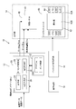
- the liquid crystal display device 10 is a display device for television reception, and includes a drive circuit 12, a display unit 14, a backlight drive circuit 16, and a power supply device 18.
- the display unit 14 includes a liquid crystal panel 40 and a backlight unit 60.
- the liquid crystal panel 40 has a display area 42 for displaying an image.
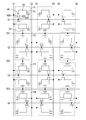
- FIG. 2 shows an equivalent circuit of the display area 42.
- the display area 42 includes a plurality of gate lines G, a plurality of source lines S, a plurality of pixels (an example of display pixels) P, and a plurality of storage capacitor lines CS.
- the gate line G is formed of a conductive material such as aluminum and is arranged in the horizontal direction on the paper surface.
- the source line S is also formed of a conductive material such as aluminum and is arranged in the vertical direction on the paper surface.
- the gate line G and the source line S are orthogonal to each other, and the pixel P is disposed at each of the portions where the gate line G and the source line S intersect.
- the pixel P is a unit display element when driving the liquid crystal panel 40, and includes two switching elements 48 and two pixel electrodes (an example of a pixel electrode) 46, respectively.
- the switching element 48 is provided with a switch electrode 48A and data electrodes 48B and 48C.
- the switch electrode 48A is connected to the corresponding gate line G
- one data electrode 48B is connected to the corresponding source line S
- the other data electrode 48C is connected to the pixel electrode 46.
- the pixel electrode 46 is an electrode formed of a conductive material such as ITO, and is disposed opposite to the counter electrode 52 connected to the ground voltage through the liquid crystal molecules sealed in the liquid crystal panel 40.
- the two switching elements 48 included in the same pixel P are connected to the same gate line G. Further, the two switching elements 48 included in the same pixel P are connected to the same source line S. The plurality of pixels P arranged side by side in the direction along the gate line G are connected to the same gate line G.
- the plurality of pixels P arranged in the direction along the source line S are not necessarily connected to the same source line S.
- two source lines S (for example, source lines S1 and S2) are provided for a plurality of pixels P arranged side by side in a direction along the source line S. W source panel ". Therefore, when any pixel P included in the plurality of pixels P is connected to one source line S, the pixel P adjacent to the pixel P in the direction along the source line S is connected to the other source line S. Has been.
- the pixels P1 and P3 are connected to the source line S1
- the pixels P2 and P4 are connected to the source line S2. It is connected.
- the storage capacitor line CS is made of a conductive material such as aluminum and is arranged in the horizontal direction on the paper surface.
- the storage capacitor line CS is disposed between the adjacent gate lines G, and is disposed between the pixels P adjacent in the direction along the source line S.
- the pixel electrode 46 included in the pixel P is insulated from the storage capacitor line CS via an insulator.
- the pixel electrode 46 is disposed opposite to the adjacent storage capacitor line CS with the insulator interposed therebetween, and the storage capacitor 50 is formed between the pixel electrode 46 and the adjacent storage capacitor line CS.
- the storage capacitor line CS forms a storage capacitor 50 between the pixel electrodes 46 of the pixels P adjacent to each other in the direction along the source line S. Therefore, the storage capacitor line CS is affected by the gate line G adjacent to the one side via the pixel electrode 46 of the pixel P adjacent to the one side in the direction along the source line S. The storage capacitor line CS is affected by the gate line G adjacent to the other side via the pixel electrode 46 of the pixel P adjacent to the other side in the direction along the source line S. That is, the storage capacitor line CS is affected by the adjacent gate lines G on both sides.
- the backlight unit 60 is disposed on the back surface of the liquid crystal panel 40.
- the backlight unit 60 includes a light source LED 64 (Light Emitting Diode) and a light guide plate 62.
- the LED 64 is disposed to face the side surface of the light guide plate 62.
- the main surface of the light guide plate 62 is disposed to face the liquid crystal panel 40.
- the side surface of the light guide plate 62 functions as a light incident surface 62 ⁇ / b> A that takes in the light emitted from the LEDs 64 into the light guide plate 62.
- the main surface of the light guide plate 62 functions as a light output surface 62 ⁇ / b> B that irradiates the liquid crystal panel 40 with light guided through the light guide plate 62.
- the backlight unit 60 is of a so-called edge light type (side light type) in which the LEDs 64 are arranged at both ends on the long side and the light guide plate 62 is arranged at the center thereof.
- the backlight drive circuit 16 is connected to a plurality of LEDs 64 constituting the backlight unit 60 and drives these LEDs 64.
- the backlight drive circuit 16 controls the amount of light incident on the light guide plate 62 from each LED 64 by supplying current to each LED 64 and controlling the amount of current supplied to the LED 64.
- the power supply device 18 is connected to the drive circuit 12 and supplies the drive circuit 12 with a plurality of reference voltages V necessary for generating various voltages necessary for display on the liquid crystal panel 40.
- the reference voltage V includes at least an on voltage Von and an off voltage Voff necessary for turning on the switching element 48 included in the pixel P of the liquid crystal panel 40.
- the drive circuit 12 includes a central processing unit (hereinafter referred to as “CPU”) 20 and a memory 22 including a ROM, a RAM, and the like.
- CPU central processing unit
- a program, a gamma function, and the like are stored in the memory 22, and the CPU 20 functions as a timer unit 24, a timing setting unit 26, a voltage generation unit 28, a voltage application unit 30, and the like according to the program read from the memory 22.
- the CPU 20 When image data configured as gradation value data is input from an external device, the CPU 20 generates various voltages necessary for display on the liquid crystal panel 40 and applies the voltages generated at a predetermined timing to the liquid crystal panel 40. .
- the CPU 20 of the drive circuit 12 starts processing when image data is input from an external device and generates various voltages (S12). At this time, the CPU 20 functions as a voltage generation unit (an example of a voltage generation circuit), and from the image data to the source line S using the reference voltage V supplied from the power supply device 18 and the gamma function stored in the memory 22. A data voltage Vd to be applied is generated.
- the CPU 20 determines the data voltage Vd corresponding to the image data using the gamma function, and generates the data voltage Vd using the reference voltage V supplied from the power supply device 18. Further, the CPU 20 generates a gate voltage (on voltage Von and off voltage Voff) to be applied to the gate line G using the reference voltage V, and a holding voltage Vc to be applied to the storage capacitor line CS.
- the CPU 20 sets the timing for applying the generated gate voltage or the like (S14). At this time, the CPU 20 functions as a timer unit 24 and a timing setting unit (an example of a setting unit) 26. After starting the liquid crystal display device 10, the CPU 20 measures an elapsed time T after the CPU 20 starts control. The CPU 20 uses the elapsed time T to set the timing for applying a voltage to the gate line G, the source line S, and the storage capacitor line CS connected to the same pixel P.
- the CPU 30 sets the timing for applying a voltage to each of a plurality of lines formed on the liquid crystal panel 40 using the elapsed time T.
- a plurality of gate lines G are formed on the liquid crystal panel 40, and by sequentially inputting an ON voltage Von to each gate line G, all the pixels P included in the liquid crystal panel 40 can be displayed.
- the CPU 20 uses the elapsed time T to switch the voltage applied to each gate line G from the off voltage Voff to the on voltage Von (ie, rise), and to switch from the on voltage Von to the off voltage Voff (ie, Set the (falling) timing.
- the CPU 20 applies the generated various voltages to the liquid crystal panel based on the set timing (S16). At this time, the CPU 20 functions as a voltage application unit.
- the CPU 20 is connected to each line provided in the liquid crystal panel 40 and applies various generated voltages to the corresponding line.
- the switching element 48 of the pixel P is switched on.
- the liquid crystal panel 40 application of the data voltage Vd to the source line S is started in synchronization with the switching element 48 of the pixel P being turned on, and the applied data voltage Vd is applied to the data electrodes 48B and 48C. Is applied to the pixel electrode 46 via When the data voltage Vd is applied to the pixel electrode 46, the liquid crystal molecules arranged corresponding to the pixel electrode 46 are deflected, and the light transmittance of the pixel P changes.
- the display unit 14 light having a predetermined luminance is emitted from the backlight unit 60 disposed on the back surface of the liquid crystal panel 40 toward the liquid crystal panel 40. Therefore, the display brightness of the pixel P can be changed by changing the transmittance of the pixel P.
- the light transmittance of the liquid crystal molecules in the pixel P can be variously changed according to the data voltage Vd, and thereby the pixel P can be controlled to a desired display luminance.
- the gate voltage applied to the gate line G is switched from the off voltage Voff to the on voltage Von, and after a predetermined display period has elapsed, the gate voltage applied to the gate line G is switched from the on voltage Von to the off voltage Voff. , The switching element 48 of the pixel P is switched off. In addition, the application of the data voltage Vd to the source line S is completed in synchronization with the switching element 48 of the pixel P being switched off. As a result, the voltage of the pixel electrode 46 is maintained at a voltage just before the switching element 48 is turned off.
- the holding voltage Vc is applied to the holding capacitor line CS. As a result, the voltage of the pixel electrode 46 is held, and the display brightness of the pixel P is held over a predetermined display period.
- a so-called “W source panel” is used as the liquid crystal panel 40, and two pixels P are controlled simultaneously. Therefore, in the liquid crystal panel 40 of the present embodiment, it is possible to simultaneously control two pixels P (for example, pixels P2 and P3) arranged side by side in the direction along the source line S. For example, when applying a voltage to the pixels P2 and P3, the voltage applied to the gate lines G2 and G3 is simultaneously switched from the off voltage to the on voltage, and the data voltage Vd corresponding to each pixel P is applied to the source lines S1 and S2. input.
- the voltage applied to the gate lines G2 and G3 is simultaneously switched from the on voltage to the off voltage.
- the pixel P1 is controlled simultaneously with the pixel P arranged on the upper side of the paper than the pixel P1
- the pixel P4 is controlled simultaneously with the pixel P arranged on the lower side of the paper than the pixel P4.
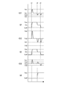
- FIG. 4 shows changes in voltages of the gate lines G1 to G4 and the storage capacitor lines CS1 to CS3 during a period in which the pixels P1 to P4 are controlled by the driving method of the present embodiment.
- Vu means the amplitude of the positive voltage side ripple generated in the storage capacitor line CS
- Vd means the amplitude of the negative voltage side ripple generated in the storage capacitor line CS.
- a constant holding voltage Vc is applied from the driving circuit 12 to each of the holding capacitor lines CS1 to CS3.
- the voltage applied to the gate line G1 is switched from the off voltage Voff to the on voltage Von (starts up) at timing t0.
- a ripple having an amplitude Vu1 is generated in the storage capacitor line CS1 connected to the pixel P1 connected to the gate line G1 via the storage capacitor 50.
- timing t1 an example of first timing
- the voltage applied to the gate line G1 is switched from the on voltage Von to the off voltage Voff (falls).
- the voltage applied to the gate lines G2 and G3 is maintained at the off voltage Voff, and the voltage applied to the gate lines G2 and G3 is not raised.
- a ripple with an amplitude Vd1 is generated in the storage capacitor line CS1.
- the voltage applied to the gate lines G2 and 3 is raised.
- a ripple having an amplitude Vu1 is generated in the storage capacitor lines CS1 and CS3.
- the storage capacitor line CS2 connected to both of the pixels P2 and 3 connected to the gate lines G2 and 3 via the storage capacitor 50 has a ripple with an amplitude Vu1 generated by the gate lines G2 and G3.
- the amplitude Vu2 is larger than the amplitude Vu1 and is approximately twice the amplitude Vu1.
- the voltage applied to the gate lines G2 and 3 is lowered.
- the voltage applied to the gate line G4 is maintained at the off voltage Voff, and the voltage applied to the gate line G4 is not raised.
- a ripple with an amplitude Vd1 is generated in the storage capacitor lines CS1 and CS3.
- the ripple having the amplitude Vd2 generated by the gate lines G2 and 3 is combined with the storage capacitor line CS2 to generate a ripple having the amplitude Vd2.
- the amplitude Vd2 is larger than the amplitude Vd1 and is approximately twice as large as the amplitude Vd1.
- timing t4 (an example of the fourth timing)
- the voltage applied to the gate line G4 is raised.
- a ripple with an amplitude Vu1 is generated in the storage capacitor line CS3.
- the rising timing of the gate line G and the falling timing of the gate line G adjacent to the gate line G are set to different timings. Therefore, when the gate voltage applied to the gate line G is changed, a ripple always occurs in the storage capacitor line CS disposed adjacent to the gate line G.
- the gate lines G1 to G4 when the rising timing of the gate line G and the falling timing of the gate line G adjacent to the gate line G are set to the same timing.
- a change in voltage of the storage capacitor lines CS1 to CS3 is shown.
- timing t1 (timing t2)
- the voltage applied to the gate line G1 is lowered and the voltages applied to the gate lines G2 and G3 are raised.
- ripples generated by the gate lines G1 and G2 cancel each other in the storage capacitor line CS1, and almost no ripples are generated.
- timing t3 (timing t4), the voltage applied to the gate lines G2 and 3 is lowered and the voltage applied to the gate line G4 is raised. As a result, ripples generated by the gate lines G3 and 4 cancel each other in the storage capacitor line CS3, and almost no ripple is generated.
- the amplitude of the ripple generated in the storage capacitor line CS arranged adjacent to the gate line G is Vu1. It is limited to two types (Vd1) and Vu2 (Vd2). As a result, compared to the case where the rising timing of the gate line G and the falling timing of the gate line G adjacent to the gate line G are set to the same timing, there is a variation in the amplitude of the ripple generated in the storage capacitor line CS. It is suppressed. Thus, for example, when the corresponding voltage Vs is input so as to cancel the generated ripple, the corresponding voltage Vs can be determined with high accuracy.
- the timing t1 at which the voltage applied to the gate line G1 is lowered and the timing t2 at which the voltage applied to the gate lines G2 and 3 are raised are set at different timings. Therefore, the ripple generated in the storage capacitor line CS1 is suppressed from being attenuated as in the case where the timing t1 and the timing t2 are set to the same timing.
- the ripple generated in the storage capacitor line CS1 is attenuated, and the ripple generated in the storage capacitor line CS2 is amplified, so that the storage capacitor line A difference in amplitude between the ripple generated in CS1 and the ripple generated in the storage capacitor line CS2 can be suppressed, and the display quality can be improved.
- the timing t3 at which the voltage applied to the gate lines G2 and 3 is lowered and the timing t4 at which the voltage applied to the gate line G4 is raised are set at different timings. Therefore, the ripple generated in the storage capacitor line CS3 is suppressed from being attenuated as in the case where the timing t3 and the timing t4 are set to the same timing.
- the ripple generated in the storage capacitor line CS3 is amplified, and the ripple generated in the storage capacitor line CS2 is attenuated, so that the storage capacitor line A difference in amplitude between the ripple generated in CS2 and the ripple generated in the storage capacitor line CS3 can be suppressed, and the display quality can be improved.
- the voltage applied to the gate line G4 is raised when the voltage applied to the gate lines G2 and 3 is lowered, the voltage applied to the gate line G4 is raised and then applied to the gate lines G2 and G3. This is different from the driving method of the liquid crystal display device 10 of the first embodiment in which the voltage applied to the gate line G4 is raised after the voltage applied to the gate lines G2 and 3 is lowered.
- the timing t1 at which the voltage applied to the gate line G1 falls and the timing t2 at which the voltage applied to the gate lines G2 and 3 are raised are set to different timings. Further, the timing t3 at which the voltage applied to the gate lines G2 and 3 is lowered and the timing t4 at which the voltage applied to the gate line G4 is raised are set to different timings. Accordingly, it is possible to suppress an increase in the difference in amplitude between the ripples generated in the storage capacitor lines CS1 and CS3 and the ripples generated in the storage capacitor line CS2, and the display quality can be improved.
- the CPU 20 functioning as the voltage generation unit 28 has a function of transforming the reference voltage V supplied from the power supply device 18.
- the drive circuit 12 includes a circuit for changing the resistance division by switching the wiring and transforming the reference voltage V, for example.
- the CPU 20 transforms the reference voltage V supplied from the power supply device 18 by using the circuit included in the drive circuit 12.
- the CPU 30 transforms the on voltage Von supplied from the power supply device 18 to generate the central voltage Vm when applying the central voltage Vm to the gate lines G2 and G3.
- the CPU 30 applies the generated central voltage Vm to the gate lines G2 and G3.
- the liquid crystal display device 10 smoothes the change in the voltage so that the influence of the dull change in voltage caused by the wiring resistance of the gate line G is affected. Is provided with a so-called “gate slope function” that suppresses flickering and improves in-plane flicker.
- the CPU 30 When switching the voltage applied to the gate line G, the CPU 30 generates a plurality of voltages between the on-voltage Von and the off-voltage Voff, thereby smoothly changing the voltage applied to the gate line G.
- the central voltage Vm is generated using this existing gate slope function. Therefore, the central voltage Vm can be generated using the function of the existing drive circuit 12.
- the voltage applied to the gate line G4 at the timing t4 is changed to the voltage applied to the gate lines G2 and 3 at the timing t3.
- the off voltage Voff is switched to the on voltage Von.
- the voltage applied to the gate line G4 is switched from the off voltage Voff to the on voltage Von, and the voltage applied to the gate lines G2 and 3 is switched from the on voltage Von to the central voltage. Switch to Vm.
- ripples are generated in the storage capacitor lines CS1, CS2, and CS3.
- a ripple with an amplitude Vd3 is generated in the storage capacitor line CS1 due to the influence from the gate line G1.
- the amplitude of the ripple generated in the storage capacitor line CS is proportional to the change in voltage generated in the adjacent gate line G. Therefore, the amplitude Vd3 is smaller than the amplitude Vd1 of the ripple generated in accordance with the switching from the on voltage Von to the off voltage Voff, and is substantially half the amplitude Vd1.
- a ripple with an amplitude Vd3 is generated from each of the gate lines G2 and 3 in the storage capacitor line CS2, and this is combined to generate a ripple with an amplitude Vd1.
- a ripple with an amplitude Vd3 from the gate line G3 and a ripple with an amplitude Vu1 from the gate line G4 are generated in the storage capacitor line CS2, and these are canceled out to generate a ripple with an amplitude Vu3.
- the amplitude Vu3 is smaller than the amplitude Vu1 and is substantially half the amplitude Vu1.
- the voltage applied to the gate line G falls, the voltage applied to the gate line G is switched from the on voltage Von to the off voltage Voff in two timings. For this reason, the amplitude of the ripple generated in the storage capacitor line CS arranged adjacent to each other is suppressed.
- the driving method of the present embodiment when the gate voltage applied to the gate line G is changed, ripples on the negative voltage side generated in the storage capacitor line CS arranged adjacent to the gate line G are reduced.
- the amplitude is limited to two types, Vd1 and Vd3, and the amplitude difference is reduced to Vd3.
- the amplitude difference can be suppressed compared to the amplitude difference Vd1 when the voltage applied to the gate line G at a time is switched from the on voltage Von to the off voltage Voff, and the ripple generated in the storage capacitor line CS can be reduced. Amplitude variation is suppressed.
- the central voltage Vm is used by using the function of generating a voltage between the on-voltage Von and the off-voltage Voff that the driving circuit 12 of the liquid crystal display device 10 has to realize the gate slope function. Is generated. Therefore, it is not necessary to newly incorporate a circuit for generating the central voltage Vm in the drive circuit 12, and the configuration of the drive circuit 12 included in the liquid crystal display device 10 can be simplified.
- the timing at which the voltage applied to the gate line G is switched from the on voltage Von to the central voltage Vm is the timing at which the voltage to be applied to the gate line G to be controlled next is switched from the off voltage Voff to the on voltage Von.
- the two timings may be set to different timings. Even in this case, the amplitude of the ripple generated in the storage capacitor line CS is limited to two types of Vu1 (Vd1) and Vu3 (Vd3), and the difference between the two types of amplitude is reduced to Vu3 (Vd3). As a result, variations in the amplitude of the ripple generated in the storage capacitor line CS are suppressed.
- the present invention is not limited to this.
- a part of the drive circuit 12 such as the CPU 20 may be disposed on the liquid crystal panel 40 as a gate driver, a source driver, or the like.
- the intermediate voltage may be set to another voltage as long as it is set to an intermediate voltage between the on voltage Von and the off voltage Voff.
- the light source using the LED 64 is exemplified, but a light source other than the LED may be used. Further, although an example using an edge light type as an arrangement of the light source is illustrated, a direct type in which the light source is arranged on the back surface of the light guide plate 62 may be used.
- SYMBOLS 10 Liquid crystal display device, 12: Drive circuit, 14: Display part, 18: Power supply device, 20: CPU, 22: Memory, 24: Time measuring part, 26: Timing setting part, 28: Voltage generation part, 30: Voltage application Part: 40: liquid crystal panel, 46: pixel electrode, 48: switching element, 50: holding capacitor, 52: counter electrode, P: pixel, G: gate line, S: source line, CS: holding capacitor line, V: reference Voltage, Von: On voltage, Voff: Off voltage, Vm: Center voltage, Vd: Data voltage, Vc: Holding voltage, Vu, Vd: Ripple amplitude
Landscapes
- Engineering & Computer Science (AREA)
- Physics & Mathematics (AREA)
- Computer Hardware Design (AREA)
- General Physics & Mathematics (AREA)
- Theoretical Computer Science (AREA)
- Chemical & Material Sciences (AREA)
- Crystallography & Structural Chemistry (AREA)
- Liquid Crystal (AREA)
- Control Of Indicators Other Than Cathode Ray Tubes (AREA)
- Liquid Crystal Display Device Control (AREA)
Abstract
本発明に係る液晶表示装置では、液晶パネルの駆動において、ゲートラインG1に印加する電圧を立ち下げてピクセルP1をオフする際に、ゲートラインG2及びゲートラインG3に印加する電圧を立ち上げてピクセルP2及びピクセルP3をオンにする。この際、ゲートラインG1に印加する電圧を立ち下げるタイミングt1と、ゲートラインG2、G3に印加する電圧を立ち上げるタイミングt3とが異なるタイミングに設定されている。この駆動方法によれば、保持容量ラインCS1に発生する振幅Vu1、Vd1のリップルが打ち消し合しあって、減衰してしまうことが抑制される。各保持容量ラインに発生するリップルの振幅の差を抑制することができ、表示品位を高めることができる。
Description
本発明は、複数の保持容量ラインの各々に発生するリップルの振幅の差を低減することで、表示品位を高める表示装置の駆動方法、表示装置の駆動装置、およびテレビ受信装置に関する。
近年、大画面テレビジョンなどの高性能な表示装置が普及しつつある(例えば、特許文献1、2)。これらの表示装置は複数の表示画素を含んでおり、表示画素にゲートライン、ソースラインなどの配線を介して信号を入力することで、表示画素を個別に制御するとともに、表示画素と保持容量ラインとの間に設けられた保持容量を用いて入力された信号を保持することで、表示装置に表示画像を形成している。
これらの表示装置では、3D表示や視野角特性の改善などの目的から、表示装置を高速に駆動する技術が求められている。表示装置を高速に駆動する方法として、いわゆる「Wソースパネル」が実現化されている。Wソースパネルでは、ソースラインに沿う方向に並ぶ各表示画素群に対してそれぞれ2本のソースラインが設けられている。そして、Wソースパネルを駆動する際には、ソースラインに沿う方法に隣接して配置された2つの表示画素を選択し、その2つの表示画素を同時に制御する。つまり、表示画素に信号を入力する場合には、隣接して配置された2本のゲートラインに印加する電圧を同時にオン電圧に切り換え、当該2本のソースラインにそれぞれ対応する信号を入力する。また、表示画素に信号を入力し終わった場合には、当該2本のゲートラインに印加する電圧を同時にオフ電圧に切り換える。Wソースパネルを備えた表示装置では、同時に2つの表示画素を制御することができ、一度に1つの表示画素しか制御できない従来の表示装置に比べ、高速駆動が可能となる。
(発明が解決しようとする課題)
しかし、Wソースパネルを備えた表示装置では、従来の表示装置に比べて保持容量ラインに発生するリップルの振幅の差が大きくなってしまう問題が生じていた。保持容量ラインは、隣接するゲートラインの間に配置され、一般に隣接するゲートラインに印加される電圧の変化に伴ってリップルが発生する。従来の表示装置では、保持容量ラインが隣接する一方のゲートラインに印加される電圧がオン電圧に切り換えられる場合、隣接する他方のゲートラインに印加される電圧はオフ電圧に切り換えられ、あるいはオフ電圧のまま維持される。そのため、保持容量ラインに発生するリップルは、隣接する両側のゲートラインの影響がお互いに打ち消された減衰したものとなるか、隣接する片側のゲートラインの影響だけによるものであった。
しかし、Wソースパネルを備えた表示装置では、従来の表示装置に比べて保持容量ラインに発生するリップルの振幅の差が大きくなってしまう問題が生じていた。保持容量ラインは、隣接するゲートラインの間に配置され、一般に隣接するゲートラインに印加される電圧の変化に伴ってリップルが発生する。従来の表示装置では、保持容量ラインが隣接する一方のゲートラインに印加される電圧がオン電圧に切り換えられる場合、隣接する他方のゲートラインに印加される電圧はオフ電圧に切り換えられ、あるいはオフ電圧のまま維持される。そのため、保持容量ラインに発生するリップルは、隣接する両側のゲートラインの影響がお互いに打ち消された減衰したものとなるか、隣接する片側のゲートラインの影響だけによるものであった。
その一方、Wソースパネルを備えた表示装置では、保持容量ラインが隣接する一方のゲートラインに印加される電圧がオン電圧に切り換えられる場合、隣接する他方のゲートラインに印加される電圧が逆にオフ電圧に切り換えられることもあれば、等しくオン電圧に切り換えられることもある。そのため、保持容量ラインに発生するリップルは、隣接する両側のゲートラインの影響がお互いに打ち消された減衰したものとなることもあれば、隣接する両側のゲートラインの影響がお互いに強め合って増幅したものとなることもあり、各保持容量ラインに発生するリップルの振幅の差が大きくなってしまう。保持容量ラインに発生するリップルの振幅の差が大きくなると、保持容量ラインとの間で保持されている表示画素の信号の電圧値がシフトする量の差が大きくなり、表示品位が低下してしまう。
本発明は、このような状況に鑑みてなされたものであり、複数の保持容量ラインに発生するリップルの振幅の差を抑制することができ、表示品位を向上させることを目的とする。
(課題を解決するための手段)
上記課題を解決するために、本発明の表示装置の駆動方法は、複数のゲートラインと複数のソースラインとが交差する部分のそれぞれに対応してスイッチング素子と画素電極とを含む表示画素が配置されるとともに、隣接する前記ゲートラインの間に配置され、前記画素電極との間で保持容量を形成する複数の保持容量ラインを備える表示装置の駆動方法であって、第1ゲートラインに接続する第1表示画素、及び前記第1ゲートラインに隣接する第2ゲートラインに接続する第2表示画素、及び前記第1ゲートラインと異なる側において前記第2ゲートラインに隣接する第3ゲートラインに接続する第3表示画素につき、前記第1ゲートラインに印加する電圧を立ち下げて前記第1表示画素をオフする際に、前記第2ゲートライン及び前記第3ゲートラインに印加する電圧を立ち上げて前記第2表示画素及び前記第3表示画素をオンしており、前記第1ゲートラインに印加する電圧を立ち下げる第1タイミングと、前記第2ゲートライン及び前記第3ゲートラインに印加する電圧を立ち上げる第2タイミングとが異なるタイミングに設定されている。
上記課題を解決するために、本発明の表示装置の駆動方法は、複数のゲートラインと複数のソースラインとが交差する部分のそれぞれに対応してスイッチング素子と画素電極とを含む表示画素が配置されるとともに、隣接する前記ゲートラインの間に配置され、前記画素電極との間で保持容量を形成する複数の保持容量ラインを備える表示装置の駆動方法であって、第1ゲートラインに接続する第1表示画素、及び前記第1ゲートラインに隣接する第2ゲートラインに接続する第2表示画素、及び前記第1ゲートラインと異なる側において前記第2ゲートラインに隣接する第3ゲートラインに接続する第3表示画素につき、前記第1ゲートラインに印加する電圧を立ち下げて前記第1表示画素をオフする際に、前記第2ゲートライン及び前記第3ゲートラインに印加する電圧を立ち上げて前記第2表示画素及び前記第3表示画素をオンしており、前記第1ゲートラインに印加する電圧を立ち下げる第1タイミングと、前記第2ゲートライン及び前記第3ゲートラインに印加する電圧を立ち上げる第2タイミングとが異なるタイミングに設定されている。
この表示装置では、隣接する第1ゲートラインと第2ゲートラインの間に配置された第1の保持容量ラインにおいて、第1ゲートラインからの影響によって第1タイミングにおいて負側に一時的に電圧が変化する負側のリップルが発生し、第2ゲートラインからの影響によって第2タイミングにおいて正側に一時的に電圧が変化する正側のリップルが発生する。また、隣接する第2ゲートラインと第3ゲートラインの間に配置された第2の保持容量ラインにおいて、第2ゲートラインからの影響によって第2タイミングにおいて正側のリップルが発生し、第3ゲートラインからの影響によって同じく第2タイミングにおいて正側のリップルが発生する。つまり、第2の保持容量ラインでは、第2タイミングにおいて第2ゲートライン及び第3ゲートラインからの影響によって発生するリップルが合成されて増幅したリップルが発生する。
この表示装置の駆動方法では、第1タイミングと第2タイミングとが異なるタイミングに設定されている。そのため、第1タイミングと第2タイミングとが同一のタイミングに設定された場合のように、第1の保持容量ラインにおいて、第1ゲートライン及び第2ゲートラインからの影響によって発生するリップルが合成されて減衰したリップルが発生することが抑制される。これによって、保持容量ラインに発生するリップルに、減衰したリップルと、増幅したリップルとが混在してしまうことがなく、各保持容量ラインに発生するリップルの振幅の差を抑制することができ、表示品位を向上させることができる。
また、上記の表示装置の駆動方法では、前記表示装置は、前記第2ゲートラインと異なる側において前記第3ゲートラインに隣接する第4ゲートラインに接続する第4表示画素を備え、前記第2ゲートライン及び前記第3ゲートラインに印加する電圧を立ち下げて前記第2表示画素及び前記第3表示画素をオフする際に、前記第4ゲートラインに印加する電圧を立ち上げて前記第4表示画素をオンしており、前記第2ゲートライン及び前記第3ゲートラインに印加する電圧を立ち下げる第3タイミングと、前記第4ゲートラインに印加する電圧を立ち上げる第4タイミングとが異なるタイミングに設定されていることが好ましい。
この表示装置では、第2の保持容量ラインにおいて、第2ゲートラインからの影響によって第3タイミングにおいて負側のリップルが発生し、第3ゲートラインからの影響によって同じく第3タイミングにおいて負側のリップルが発生する。つまり、第2の保持容量ラインでは、第3タイミングにおいて第2ゲートライン及び第3ゲートラインからの影響によって発生するリップルが合成されて増幅したリップルが発生する。また、隣接する第3ゲートラインと第4ゲートラインの間に配置された第3の保持容量ラインにおいて、第3ゲートラインからの影響によって第3タイミングにおいて負側のリップルが発生し、第4ゲートラインからの影響によって第4タイミングにおいて正側のリップルが発生する。
この表示装置の駆動方法では、第3タイミングと第4タイミングとが異なるタイミングに設定されている。そのため、第3タイミングと第4タイミングとが同一のタイミングに設定された場合のように、第3の保持容量ラインにおいて、第3ゲートライン及び第4ゲートラインからの影響によって発生するリップルが合成されて減衰したリップルが発生することが抑制される。これによって、保持容量ラインに発生するリップルに、増幅したリップルと、減衰したリップルとが混在してしまうことがなく、各保持容量ラインに発生するリップルの振幅の差を抑制することができ、表示品位を向上させることができる。
また、上記の表示装置の駆動方法では、前記第2ゲートライン及び前記第3ゲートラインに印加する電圧を立ち下げる際に、前記第3タイミングに先立つ第5タイミングにおいて、前記第2ゲートライン及び前記第3ゲートラインに印加する電圧をオン電圧からオン電圧とオフ電圧の間の電圧に設定されている中間電圧に切り換え、前記第3タイミングにおいて、前記第2ゲートライン及び前記第3ゲートラインに印加する電圧を中間電圧からオフ電圧に切り換えて立ち下げることが好ましい。
この表示装置の駆動方法では、第2ゲートライン及び第3ゲートラインに印加する電圧を立ち下げる際に、第5タイミングと第3タイミングの2回に分けて当該ゲートラインに印加する電圧をオン電圧からオフ電圧へと切り換える。そのため、第3タイミングでオン電圧からオフ電圧へと切り換える場合に比べて、第3タイミングにおける電圧の変化量を抑えることができる。一般に、保持容量ラインに発生するリップルの振幅は、ゲートラインに印加される電圧の変化量に比例する。この表示装置の駆動方法によれば、第3タイミングにおける第2ゲートライン及び第3ゲートラインに印加される電圧の変化量を抑えることで、第3タイミングにおいて第2の保持容量ラインに発生する増幅したリップルの振幅を抑えることができる。これによって、各保持容量ラインに発生するリップルの振幅の差を抑制することができ、表示品位を向上させることができる。
また、上記の表示装置の駆動方法では、前記表示装置が、前記表示画素が形成された基板に対向して配置され、対向電極が設けられた対向基板と、対向配置される前記表示画素の画素電極と前記対向電極との間に発生するフリッカを制御する際に前記ゲートラインに印加される電圧を生成する電圧生成回路と、を備えていても良い。この場合、前記電圧生成回路は、前記第5タイミングにおいて前記ゲートラインに印加される中間電圧を生成する回路を兼ねることが好ましい。
表示装置の表示画素に含まれる画素電極と対向電極との間にフリッカが発生した場合に、表示画素に接続するゲートラインに中間電圧等を印加して、フリッカを低減させる技術が知られている。上記技術を実現可能な表示装置では、ゲートラインに中間電圧等を生成する回路が備えられており、その回路を用いてゲートラインに印加する中間電圧等を生成する。この表示装置の駆動方法では、表示装置のフリッカを低減させるために備えられた回路を用いて、各保持容量ラインに発生するリップルの振幅の差を抑制するための中間電圧を生成するので、表示装置を簡略化して構成することができる。
本発明は、上記の表示装置の駆動方法を実現する表示装置の駆動装置にも具現化される。本発明の表示装置の駆動装置は、複数のゲートラインと複数のソースラインとが交差する部分のそれぞれに対応してスイッチング素子と画素電極とを含む表示画素が配置されるとともに、隣接する前記ゲートラインの間に配置され、前記画素電極との間で保持容量を形成する複数の保持容量ラインを備える表示装置の駆動装置であって、前記ゲートラインに電圧を印加する電圧印加部と、前記電圧印加部が前記ゲートラインに電圧を印加するタイミングを設定する設定部を備える。前記電圧印加部は、第1ゲートラインに接続する第1表示画素、及び前記第1ゲートラインに隣接する第2ゲートラインに接続する第2表示画素、及び前記第1ゲートラインと異なる側において前記第2ゲートラインに隣接する第3ゲートラインに接続する第3表示画素につき、前記第1ゲートラインに印加する電圧を立ち下げて前記第1表示画素をオフする際に、前記第2ゲートライン及び前記第3ゲートラインに印加する電圧を立ち上げて前記第2表示画素及び前記第3表示画素をオンする。前記設定部は、前記第1ゲートラインに印加する電圧を立ち下げる第1タイミングと、前記第2ゲートライン及び前記第3ゲートラインに印加する電圧を立ち上げる第2タイミングとが異なるタイミングに設定する。
この表示装置の駆動装置を用いることで、第1タイミングと第2タイミングとが同一のタイミングに設定される。そのため、保持容量ラインに発生するリップルに、減衰したリップルと、増幅したリップルとが混在してしまうことが抑制される。これによって、各保持容量ラインに発生するリップルの振幅の差を抑制することができ、表示品位を向上させることができる。
また、上記の表示装置の駆動装置では、前記表示装置が液晶パネルを用いた液晶表示装置であることが好ましい。この表示装置の駆動装置によれば、液晶パネル内に設けられた複数の保持容量ラインにおいて、各保持容量ラインに発生するリップルの振幅の差を抑制することができ、液晶パネルを用いた液晶表示装置の表示品位を向上させることができる。
本発明は、上記の表示装置の駆動回路と、表示装置とを備えるテレビ受信装置にも具現化される。このテレビ受信装置によれば、表示装置内に設けられた複数の保持容量ラインにおいて、各保持容量ラインに発生するリップルの振幅の差を抑制することができ、テレビ受信装置の表示品位を向上させることができる。
(発明の効果)
本発明によれば、複数の保持容量ラインの各々に発生するリップルの振幅の差を抑制することができ、表示品位を向上させることができる。
本発明によれば、複数の保持容量ラインの各々に発生するリップルの振幅の差を抑制することができ、表示品位を向上させることができる。
<実施形態1>
本発明の実施形態1を、図面を参照して説明する。
(1.液晶表示装置の構成)
図1に示すように、液晶表示装置10は、テレビ受信用の表示装置であり、駆動回路12と表示部14とバックライト駆動回路16と電源装置18を含んでいる。表示部14は、液晶パネル40とバックライトユニット60を含んで構成されている。
液晶パネル40には、画像を表示する表示領域42を有する。図2に、表示領域42の等価回路を示す。表示領域42は、複数のゲートラインG、複数のソースラインS、複数のピクセル(表示画素の一例)P、複数の保持容量ラインCSを含む。ゲートラインGは、アルミなどの導電性材料で形成されており、紙面横方向に配置されている。ソースラインSは、同じくアルミなどの導電性材料で形成されており、紙面縦方向に配置されている。表示領域42において、ゲートラインGとソースラインSは直交しており、ゲートラインGとソースラインSとが交差する部分のそれぞれにピクセルPが配置されている。
本発明の実施形態1を、図面を参照して説明する。
(1.液晶表示装置の構成)
図1に示すように、液晶表示装置10は、テレビ受信用の表示装置であり、駆動回路12と表示部14とバックライト駆動回路16と電源装置18を含んでいる。表示部14は、液晶パネル40とバックライトユニット60を含んで構成されている。
液晶パネル40には、画像を表示する表示領域42を有する。図2に、表示領域42の等価回路を示す。表示領域42は、複数のゲートラインG、複数のソースラインS、複数のピクセル(表示画素の一例)P、複数の保持容量ラインCSを含む。ゲートラインGは、アルミなどの導電性材料で形成されており、紙面横方向に配置されている。ソースラインSは、同じくアルミなどの導電性材料で形成されており、紙面縦方向に配置されている。表示領域42において、ゲートラインGとソースラインSは直交しており、ゲートラインGとソースラインSとが交差する部分のそれぞれにピクセルPが配置されている。
ピクセルPは、液晶パネル40を駆動する際の単位表示素子であり、それぞれ2つのスイッチング素子48と2つのピクセル電極(画素電極の一例)46を含む。スイッチング素子48には、スイッチ電極48Aとデータ電極48B、48Cが設けられている。スイッチ電極48Aは対応するゲートラインGに接続されており、一方のデータ電極48Bは対応するソースラインSに接続されており、他方のデータ電極48Cはピクセル電極46に接続されている。ピクセル電極46は、ITOなどの導電性材料で形成された電極であり、液晶パネル40内に封入された液晶分子を介して接地電圧に接続された対向電極52に対向配置されている。
同一のピクセルPに含まれる2つのスイッチング素子48は、同一のゲートラインGに接続される。また、同一のピクセルPに含まれる2つのスイッチング素子48は、同一のソースラインSに接続されている。ゲートラインGに沿う方向に並んで配置されている複数のピクセルPは、同一のゲートラインGに接続されている。
その一方、ソースラインSに沿う方向に並んで配置されている複数のピクセルPは、必ずしも同一のソースラインSに接続されない。本実施形態の液晶パネル40は、ソースラインSに沿う方向に並んで配置されている複数のピクセルPに対して2本のソースラインS(例えば、ソースラインS1、S2)が設けられる、いわゆる「Wソースパネル」である。そのため、当該複数のピクセルPに含まれる任意のピクセルPが一方のソースラインSに接続されている場合、そのピクセルPにソースラインSに沿う方向に隣接するピクセルPは他方のソースラインSに接続されている。つまり、ソースラインS1、S2に沿う方向に並んで配置されているピクセルP1、P2、P3,P4において、ピクセルP1、P3がソースラインS1に接続されており、ピクセルP2、P4がソースラインS2に接続されている。
保持容量ラインCSは、アルミなどの導電性材料で形成されており、紙面横方向に配置されている。保持容量ラインCSは、隣接するゲートラインGの間に配置されるとともに、ソースラインSに沿う方向に隣接するピクセルPの間に配置されている。ピクセルPに含まれるピクセル電極46は、絶縁体を介して保持容量ラインCSから絶縁されている。ピクセル電極46は、当該絶縁体を介して隣接する保持容量ラインCSと対向配置されており、ピクセル電極46と隣接する保持容量ラインCSとの間に保持容量50が形成されている。
保持容量ラインCSは、ソースラインSに沿う方向において隣接する両側のピクセルPのピクセル電極46との間に保持容量50を形成している。そのため、保持容量ラインCSは、ソースラインSに沿う方向の一方側に隣接するピクセルPのピクセル電極46を介して、当該一方側に隣接するゲートラインGからの影響を受ける。また、保持容量ラインCSは、ソースラインSに沿う方向の他方側に隣接するピクセルPのピクセル電極46を介して、当該他方側に隣接するゲートラインGからの影響を受ける。つまり、保持容量ラインCSは、隣接する両側のゲートラインGからの影響を受ける。
バックライトユニット60は、液晶パネル40の背面に配置されている。バックライトユニット60は、光源であるLED64(Light Emitting Diode:発光ダイオード)と、導光板62を備えている。LED64は、導光板62の側面に対向して配置されている。導光板62は、その主面が液晶パネル40に対向して配置されている。導光板62では、LED64から側面に入射された光を液晶パネル40に対向する主面に導光している。そのため、導光板62の側面は、LED64から照射された光を導光板62内に取り込む入光面62Aとして機能している。また導光板62の主面は、導光板62内を導光した光を液晶パネル40へと照射する出光面62Bとして機能している。このようにバックライトユニット60は、その長辺側の両端部にLED64が配置され、その中央に導光板62を配してなる、いわゆるエッジライト型(サイドライト型)とされている。
バックライト駆動回路16は、バックライトユニット60を構成する複数のLED64に接続されており、これらLED64を駆動している。バックライト駆動回路16は、各LED64に電流を供給し、LED64に供給する電流量を制御することによって、各LED64から導光板62に入光される光量を制御している。
電源装置18は、駆動回路12に接続されており、液晶パネル40の表示に必要な各種電圧を生成するのに必要な複数の基準電圧Vを駆動回路12に供給している。基準電圧Vには、少なくとも液晶パネル40のピクセルPに含まれるスイッチング素子48をオンさせるのに必要なオン電圧Von及びオフ電圧Voffを備える。
駆動回路12は、中央処理装置(以下「CPU」という)20、ROM、RAM等からなるメモリ22を含む。メモリ22には、プログラム、ガンマ関数等が記憶されており、CPU20は、メモリ22から読み出したプログラムに従って、計時部24、タイミング設定部26、電圧生成部28、電圧印加部30等として機能する。CPU20は、外部装置から階調値データとして構成される画像データが入力されると、液晶パネル40の表示に必要な各種電圧を生成し、所定のタイミングで生成した電圧を液晶パネル40に印加する。
(2.表示処理)
図3ないし図6を用いて、液晶表示装置10の表示処理を説明する。
図3に示すように、駆動回路12のCPU20は、外部装置から画像データが入力されると処理を開始し、各種電圧を生成する(S12)。この際、CPU20は電圧生成部(電圧生成回路の一例)として機能し、電源装置18から供給される基準電圧V、及びメモリ22に記憶されたガンマ関数を用いて、画像データからソースラインSに印加するデータ電圧Vdを生成する。CPU20は、ガンマ関数を用いて画像データに対応するデータ電圧Vdを決定し、電源装置18から供給される基準電圧Vを用いてそのデータ電圧Vdを生成する。また、CPU20は、基準電圧Vを用いてゲートラインGに印加するゲート電圧(オン電圧Von及びオフ電圧Voff)、及び保持容量ラインCSに印加する保持電圧Vcを生成する。
図3ないし図6を用いて、液晶表示装置10の表示処理を説明する。
図3に示すように、駆動回路12のCPU20は、外部装置から画像データが入力されると処理を開始し、各種電圧を生成する(S12)。この際、CPU20は電圧生成部(電圧生成回路の一例)として機能し、電源装置18から供給される基準電圧V、及びメモリ22に記憶されたガンマ関数を用いて、画像データからソースラインSに印加するデータ電圧Vdを生成する。CPU20は、ガンマ関数を用いて画像データに対応するデータ電圧Vdを決定し、電源装置18から供給される基準電圧Vを用いてそのデータ電圧Vdを生成する。また、CPU20は、基準電圧Vを用いてゲートラインGに印加するゲート電圧(オン電圧Von及びオフ電圧Voff)、及び保持容量ラインCSに印加する保持電圧Vcを生成する。
次に、CPU20は、生成したゲート電圧等を印加するタイミングを設定する(S14)。この際、CPU20は計時部24及びタイミング設定部(設定部の一例)26として機能する。CPU20は、液晶表示装置10を起動後、CPU20が制御を開始してからの経過時間Tを計時している。CPU20は、経過時間Tを用いて、同一のピクセルPに接続されるゲートラインG、ソースラインS、保持容量ラインCSに電圧を印加するタイミングを設定する。
また、CPU30は、経過時間Tを用いて、液晶パネル40に複数本形成されたラインの各々に電圧を印加するタイミングを設定する。例えば、液晶パネル40には複数のゲートラインGが形成されており、各々のゲートラインGに順次オン電圧Vonを入力することで、液晶パネル40に含まれる全てのピクセルPが表示可能となる。CPU20は、経過時間Tを用いて、各々のゲートラインGに印加する電圧をオフ電圧Voffからオン電圧Vonに切り換える(すなわち、立ち上げ)タイミングと、オン電圧Vonからオフ電圧Voffに切り換える(すなわち、立ち下げ)タイミングと、を設定する。
次に、CPU20は、設定したタイミングに基づいて、生成した各種電圧を液晶パネルに印加する(S16)。この際、CPU20は電圧印加部として機能する。CPU20は、液晶パネル40に設けられた各ラインに接続されており、生成した各種電圧を対応するラインに印加する。
液晶パネル40では、制御の対象となるピクセルPのゲートラインGに印加されるゲート電圧がオフ電圧Voffからオン電圧Vonに切り換わると、ピクセルPのスイッチング素子48がオンに切り換わる。
また、液晶パネル40では、ピクセルPのスイッチング素子48がオンに切り換わるのに同期して、ソースラインSへのデータ電圧Vdの印加が開始され、印加されたデータ電圧Vdがデータ電極48B、48Cを介してピクセル電極46に印加される。データ電圧Vdがピクセル電極46に印加されると、ピクセル電極46に対応配置された液晶分子が偏向し、ピクセルPの光透過率が変化する。表示部14では、液晶パネル40の背面に配置されているバックライトユニット60から液晶パネル40に向かって所定輝度の光が照射されている。そのため、ピクセルPの透過率が変化することで、ピクセルPの表示輝度を変化させることができる。ピクセルPにおける液晶分子の光透過率は、データ電圧Vdによって種々に変化させることができ、これによって、ピクセルPを所望の表示輝度に制御することができる。
ゲートラインGに印加されるゲート電圧がオフ電圧Voffからオン電圧Vonに切り換わってから所定の表示期間経過後、ゲートラインGに印加されるゲート電圧がオン電圧Vonからオフ電圧Voffに切り換わると、ピクセルPのスイッチング素子48がオフに切り換わる。また、ピクセルPのスイッチング素子48がオフに切り換わるのに同期して、ソースラインSへのデータ電圧Vdの印加が終了される。これによって、ピクセル電極46の電圧が、スイッチング素子48をオフする直前の電圧に維持される。
また、ピクセル電極46にデータ電圧Vdが印加されるのに先だって、保持容量ラインCSに保持電圧Vcが印加されている。これによってピクセル電極46の電圧が保持され、所定の表示期間に亘ってピクセルPの表示輝度が保持される。
(3.印加タイミング)
図2に示すように、本実施形態では、液晶パネル40としていわゆる「Wソースパネル」を用いており、同時に2つのピクセルPを制御している。そのため、本実施形態の液晶パネル40では、ソースラインSに沿う方向に並んで配置されている2つのピクセルP(例えばピクセルP2、P3)を同時に制御することが可能である。例えば、ピクセルP2、P3に電圧を印加する際には、ゲートラインG2、G3に印加する電圧を同時にオフ電圧からオン電圧に切り換え、ソースラインS1、S2に各ピクセルPに対応したデータ電圧Vdを入力する。また、ピクセルP2、P3に電圧を印加するのを終える際には、ゲートラインG2、G3に印加する電圧を同時にオン電圧からオフ電圧に切り換える。同様に、ピクセルP1はピクセルP1よりも紙面上側に配置されたピクセルPと同時に制御されており、ピクセルP4はピクセルP4よりも紙面下側に配置されたピクセルPと同時に制御されている。
図2に示すように、本実施形態では、液晶パネル40としていわゆる「Wソースパネル」を用いており、同時に2つのピクセルPを制御している。そのため、本実施形態の液晶パネル40では、ソースラインSに沿う方向に並んで配置されている2つのピクセルP(例えばピクセルP2、P3)を同時に制御することが可能である。例えば、ピクセルP2、P3に電圧を印加する際には、ゲートラインG2、G3に印加する電圧を同時にオフ電圧からオン電圧に切り換え、ソースラインS1、S2に各ピクセルPに対応したデータ電圧Vdを入力する。また、ピクセルP2、P3に電圧を印加するのを終える際には、ゲートラインG2、G3に印加する電圧を同時にオン電圧からオフ電圧に切り換える。同様に、ピクセルP1はピクセルP1よりも紙面上側に配置されたピクセルPと同時に制御されており、ピクセルP4はピクセルP4よりも紙面下側に配置されたピクセルPと同時に制御されている。
図4に、本実施形態の駆動方法による、ピクセルP1~P4が制御される期間におけるゲートラインG1~G4及び保持容量ラインCS1~CS3の電圧の変化を示す。ここで、Vuは、保持容量ラインCSに発生する正電圧側のリップルの振幅を意味しており、Vdは、保持容量ラインCSに発生する負電圧側のリップルの振幅を意味している。また、図4に示す期間において、駆動回路12から保持容量ラインCS1~CS3の各々に、一定の保持電圧Vcが印加されている。
図4に示すように、本実施形態の駆動方法では、タイミングt0においてゲートラインG1に印加する電圧をオフ電圧Voffからオン電圧Vonに切り換える(立ち上げる)。これによって、ゲートラインG1に接続されているピクセルP1に保持容量50を介して接続されている保持容量ラインCS1に振幅Vu1のリップルが発生する。
次に、タイミングt1(第1タイミングの一例)において、ゲートラインG1に印加する電圧をオン電圧Vonからオフ電圧Voffに切り換える(立ち下げる)。この際、ゲートラインG2、G3に印加する電圧をオフ電圧Voffに維持し、ゲートラインG2、G3に印加する電圧を立ち上げない。これによって、保持容量ラインCS1に振幅Vd1のリップルが発生する。
次に、タイミングt2(第2タイミングの一例)において、ゲートラインG2、3に印加する電圧を立ち上げる。これによって、保持容量ラインCS1、3に振幅Vu1のリップルが発生する。また、ゲートラインG2、3に接続されているピクセルP2、3の双方に保持容量50を介して接続されている保持容量ラインCS2には、各々のゲートラインG2、3により発生する振幅Vu1のリップルが合成されて、振幅Vu2のリップルが発生する。振幅Vu2は、振幅Vu1よりも大きく、振幅Vu1の略2倍の振幅となる。
次に、タイミングt3(第3タイミングの一例)において、ゲートラインG2、3に印加する電圧を立ち下げる。この際、ゲートラインG4に印加する電圧をオフ電圧Voffに維持し、ゲートラインG4に印加する電圧を立ち上げない。これによって、保持容量ラインCS1、3に振幅Vd1のリップルが発生する。また、保持容量ラインCS2には、各々のゲートラインG2、3により発生する振幅Vd1のリップルが合成されて、振幅Vd2のリップルが発生する。振幅Vd2は、振幅Vd1よりも大きく、振幅Vd1の略2倍の振幅となる。
次に、タイミングt4(第4タイミングの一例)において、ゲートラインG4に印加する電圧を立ち上げる。これによって、保持容量ラインCS3に振幅Vu1のリップルが発生する。
次に、タイミングt5において、ゲートラインG4に印加する電圧を立ち下げる。これによって、保持容量ラインCS3に振幅Vd1のリップルが発生する。
本実施形態の駆動方法では、ゲートラインGの立ち上げタイミングと、そのゲートラインGに隣接するゲートラインGの立ち下げタイミングを異なるタイミングに設定している。そのため、ゲートラインGに印加されるゲート電圧を変化させると、そのゲートラインGに隣接して配置される保持容量ラインCSに必ずリップルが発生している。
図5に、本実施形態の駆動方法と異なり、ゲートラインGの立ち上げタイミングと、そのゲートラインGに隣接するゲートラインGの立ち下げタイミングを等しいタイミングに設定した場合のゲートラインG1~G4及び保持容量ラインCS1~CS3の電圧の変化を示す。
この場合、タイミングt1(タイミングt2)において、ゲートラインG1に印加する電圧を立ち下げるとともに、ゲートラインG2、G3に印加する電圧を立ち上げる。これによって、保持容量ラインCS1には、各々のゲートラインG1、2により発生するリップルが打ち消しあい、ほぼリップルが発生しない。
また、タイミングt3(タイミングt4)において、ゲートラインG2、3に印加する電圧を立ち下げるとともに、ゲートラインG4に印加する電圧を立ち上げる。これによって、保持容量ラインCS3には、各々のゲートラインG3、4により発生するリップルが打ち消しあい、ほぼリップルが発生しない。
ゲートラインGの立ち上げタイミングと、そのゲートラインGに隣接するゲートラインGの立ち下げタイミングを等しいタイミングに設定した場合、ゲートラインGに印加されるゲート電圧を変化させたとしても、そのゲートラインGに隣接して配置される保持容量ラインCSにリップルが発生しない(つまり、振幅が「0」のリップルが発生する)ことがある。そのため、ゲートラインGに印加されるゲート電圧を変化させた場合に、そのゲートラインGに隣接して配置される保持容量ラインCSに発生するリップルの振幅は、0、Vu1(Vd1)、Vu2(Vd2)の3種類の1つとなる。
一方、本実施形態の駆動方法では、ゲートラインGに印加されるゲート電圧を変化させた場合に、そのゲートラインGに隣接して配置される保持容量ラインCSに発生するリップルの振幅は、Vu1(Vd1)、Vu2(Vd2)の2種類に限られる。これによって、ゲートラインGの立ち上げタイミングと、そのゲートラインGに隣接するゲートラインGの立ち下げタイミングを等しいタイミングに設定した場合に比べて、保持容量ラインCSに発生するリップルの振幅のバラツキが抑制される。これによって、例えば発生するリップルを打ち消すように対応電圧Vsを入力する場合に、対応電圧Vsを精度よく決定することが可能である。
(4.本実施形態の効果)
(1)本実施形態では、ゲートラインG1に印加する電圧を立ち下げるタイミングt1と、ゲートラインG2、3に印加する電圧を立ち上げるタイミングt2と、が異なるタイミングに設定されている。そのため、タイミングt1とタイミングt2とが同一のタイミングに設定された場合のように、保持容量ラインCS1に発生するリップルが減衰してしまうことが抑制される。これによって、タイミングt1とタイミングt2とが同一のタイミングに設定された場合のように、保持容量ラインCS1では発生するリップルが減衰し、保持容量ラインCS2では発生するリップルが増幅して、保持容量ラインCS1に発生するリップルと保持容量ラインCS2に発生するリップルの振幅の差を抑制することができ、表示品位を向上させることができる。
(1)本実施形態では、ゲートラインG1に印加する電圧を立ち下げるタイミングt1と、ゲートラインG2、3に印加する電圧を立ち上げるタイミングt2と、が異なるタイミングに設定されている。そのため、タイミングt1とタイミングt2とが同一のタイミングに設定された場合のように、保持容量ラインCS1に発生するリップルが減衰してしまうことが抑制される。これによって、タイミングt1とタイミングt2とが同一のタイミングに設定された場合のように、保持容量ラインCS1では発生するリップルが減衰し、保持容量ラインCS2では発生するリップルが増幅して、保持容量ラインCS1に発生するリップルと保持容量ラインCS2に発生するリップルの振幅の差を抑制することができ、表示品位を向上させることができる。
(2)本実施形態では、ゲートラインG2、3に印加する電圧を立ち下げるタイミングt3と、ゲートラインG4に印加する電圧を立ち上げるタイミングt4と、が異なるタイミングに設定されている。そのため、タイミングt3とタイミングt4とが同一のタイミングに設定された場合のように、保持容量ラインCS3に発生するリップルが減衰してしまうことが抑制される。これによって、タイミングt3とタイミングt4とが同一のタイミングに設定された場合のように、保持容量ラインCS3では発生するリップルが増幅し、保持容量ラインCS2では発生するリップルが減衰して、保持容量ラインCS2に発生するリップルと保持容量ラインCS3に発生するリップルの振幅の差を抑制することができ、表示品位を向上させることができる。
<実施形態2>
本発明の実施形態2を、図6を用いて説明する。
(1.印加タイミング)
本実施形態の液晶表示装置10の駆動方法では、ゲートラインG1に印加する電圧を立ち下げる際に、ゲートラインG2、3に印加する電圧を立ち上げる場合において、ゲートラインG2、3に印加する電圧を立ち上げた後に、ゲートラインG1に印加する電圧を立ち下げる点で、ゲートラインG1に印加する電圧を立ち下げた後に、ゲートラインG2、3に印加する電圧を立ち上げる実施形態1の液晶表示装置10の駆動方法と異なる。また、ゲートラインG2、3に印加する電圧を立ち下げる際に、ゲートラインG4に印加する電圧を立ち上げる場合において、ゲートラインG4に印加する電圧を立ち上げた後に、ゲートラインG2、3に印加する電圧を立ち下げる点で、ゲートラインG2、3に印加する電圧を立ち下げた後に、ゲートラインG4に印加する電圧を立ち上げる実施形態1の液晶表示装置10の駆動方法と異なる。
本発明の実施形態2を、図6を用いて説明する。
(1.印加タイミング)
本実施形態の液晶表示装置10の駆動方法では、ゲートラインG1に印加する電圧を立ち下げる際に、ゲートラインG2、3に印加する電圧を立ち上げる場合において、ゲートラインG2、3に印加する電圧を立ち上げた後に、ゲートラインG1に印加する電圧を立ち下げる点で、ゲートラインG1に印加する電圧を立ち下げた後に、ゲートラインG2、3に印加する電圧を立ち上げる実施形態1の液晶表示装置10の駆動方法と異なる。また、ゲートラインG2、3に印加する電圧を立ち下げる際に、ゲートラインG4に印加する電圧を立ち上げる場合において、ゲートラインG4に印加する電圧を立ち上げた後に、ゲートラインG2、3に印加する電圧を立ち下げる点で、ゲートラインG2、3に印加する電圧を立ち下げた後に、ゲートラインG4に印加する電圧を立ち上げる実施形態1の液晶表示装置10の駆動方法と異なる。
(2.本実施形態の効果)
(1)本実施形態でも、ゲートラインG1に印加する電圧を立ち下げるタイミングt1と、ゲートラインG2、3に印加する電圧を立ち上げるタイミングt2と、が異なるタイミングに設定されている。また、ゲートラインG2、3に印加する電圧を立ち下げるタイミングt3と、ゲートラインG4に印加する電圧を立ち上げるタイミングt4と、が異なるタイミングに設定されている。これによって、保持容量ラインCS1、3に発生するリップルと保持容量ラインCS2に発生するリップルの振幅の差が拡大してしまうことを抑制することができ、表示品位を向上させることができる。
(1)本実施形態でも、ゲートラインG1に印加する電圧を立ち下げるタイミングt1と、ゲートラインG2、3に印加する電圧を立ち上げるタイミングt2と、が異なるタイミングに設定されている。また、ゲートラインG2、3に印加する電圧を立ち下げるタイミングt3と、ゲートラインG4に印加する電圧を立ち上げるタイミングt4と、が異なるタイミングに設定されている。これによって、保持容量ラインCS1、3に発生するリップルと保持容量ラインCS2に発生するリップルの振幅の差が拡大してしまうことを抑制することができ、表示品位を向上させることができる。
(2)本実施形態では、ピクセルP1にオン電圧Vonが印加される期間の一部と、ピクセルP1の次に制御されるピクセルP3にオン電圧Vonが印加される期間の一部とが、重なるように設定されている。同様に、ピクセルP2にオン電圧Vonが印加される期間の一部と、ピクセルP2の次に制御されるピクセルP4にオン電圧Vonが印加される期間の一部とが、重なるように設定されている。これによって、ピクセルP1(P2)を制御した後にピクセルP3(P4)を制御する場合において、そのいずれものピクセルPにオン電圧Vonが印加されておらず、制御不能な期間を省くことができ、液晶表示装置10を高速に駆動することが可能である。
(3)本実施形態では、同時に制御することを意図しない複数のピクセルPに同時にオン電圧Vonが印加される期間が存在する。そのため、本実施形態では、1つ前に制御されるピクセルPのスイッチング素子48がオフに切り換わるのと同期して、ソースラインSへのデータ電圧Vdの印加を開始する。また、1つ後に制御されるピクセルPのスイッチング素子48がオンに切り換わるのに先立って、ソースラインSへのデータ電圧Vdの印加を終了する。これによって、ピクセルPに意図しないデータ電圧Vdが印加されることが防止される。
<実施形態3>
本発明の実施形態3を、図7を用いて説明する。本実施形態の液晶表示装置10の駆動方法では、ゲートラインGに印加する電圧をオン電圧Vonからオフ電圧Voffに切り換える際に、まずオン電圧Vonからオン電圧Vonとオフ電圧Voffの中央の電圧に設定された中央電圧(中間電圧の一例)Vm(=(Von+Voff)/2)に切り換え、次に、中央電圧Vmに切り換えたタイミングと異なるタイミングで中央電圧Vmからオフ電圧Voffに切り換える点で、一度にオン電圧Vonからオフ電圧Voffに切り換える実施形態2の液晶表示装置10の駆動方法と異なる。以下では、ゲートラインG2、3に印加する電圧を異なる2回のタイミングでオン電圧Vonからオフ電圧Voffに切り換える例を用いて説明する。
本発明の実施形態3を、図7を用いて説明する。本実施形態の液晶表示装置10の駆動方法では、ゲートラインGに印加する電圧をオン電圧Vonからオフ電圧Voffに切り換える際に、まずオン電圧Vonからオン電圧Vonとオフ電圧Voffの中央の電圧に設定された中央電圧(中間電圧の一例)Vm(=(Von+Voff)/2)に切り換え、次に、中央電圧Vmに切り換えたタイミングと異なるタイミングで中央電圧Vmからオフ電圧Voffに切り換える点で、一度にオン電圧Vonからオフ電圧Voffに切り換える実施形態2の液晶表示装置10の駆動方法と異なる。以下では、ゲートラインG2、3に印加する電圧を異なる2回のタイミングでオン電圧Vonからオフ電圧Voffに切り換える例を用いて説明する。
(1.液晶表示装置の構成)
本実施形態の液晶表示装置10では、電圧生成部28として機能するCPU20が、電源装置18から供給される基準電圧Vを変圧する機能を有する。駆動回路12には、例えば配線の切り換えにより抵抗分割を変更し、基準電圧Vを変圧する等の回路が含まれる。CPU20は、駆動回路12に含まれる当該回路を用いて、電源装置18から供給される基準電圧Vを変圧する。
本実施形態の液晶表示装置10では、電圧生成部28として機能するCPU20が、電源装置18から供給される基準電圧Vを変圧する機能を有する。駆動回路12には、例えば配線の切り換えにより抵抗分割を変更し、基準電圧Vを変圧する等の回路が含まれる。CPU20は、駆動回路12に含まれる当該回路を用いて、電源装置18から供給される基準電圧Vを変圧する。
CPU30は、ゲートラインG2、3に中央電圧Vmを印加する際に、電源装置18から供給されるオン電圧Vonを変圧して中央電圧Vmを生成する。CPU30は、この生成した中央電圧VmをゲートラインG2、3に印加する。
また、液晶表示装置10は、液晶パネル40のゲートラインGに印加する電圧を切り換える際に、その電圧の変化をなだらかにすることで、ゲートラインGの配線抵抗によって生じる電圧の変化の鈍りの影響を抑制し、面内フリッカを改善する、いわゆる「ゲートスロープ機能」を備える。CPU30は、ゲートラインGに印加される電圧を切り換える際に、オン電圧Vonとオフ電圧Voffの間の複数の電圧を生成することで、ゲートラインGに印加する電圧をなだらかに変化させている。
本実施形態の液晶表示装置10では、この既存のゲートスロープ機能を用いて中央電圧Vmを生成する。そのため、既存の駆動回路12が有している機能を用いて、中央電圧Vmを生成することができる。
(2.印加タイミング)
図7に示すように、本実施形態の駆動方法では、タイミングt3において、ゲートラインG2、3に印加する電圧をオフ電圧Voffに切り換えるに先立って、タイミングt4において、ゲートラインG4に印加する電圧をオフ電圧Voffからオン電圧Vonに切り換える。この際、タイミングt4(第5のタイミングの一例)において、ゲートラインG4に印加する電圧をオフ電圧Voffからオン電圧Vonに切り換えるとともに、ゲートラインG2、3に印加する電圧をオン電圧Vonから中央電圧Vmに切り換える。これによって、保持容量ラインCS1、CS2、CS3にリップルが発生する。
図7に示すように、本実施形態の駆動方法では、タイミングt3において、ゲートラインG2、3に印加する電圧をオフ電圧Voffに切り換えるに先立って、タイミングt4において、ゲートラインG4に印加する電圧をオフ電圧Voffからオン電圧Vonに切り換える。この際、タイミングt4(第5のタイミングの一例)において、ゲートラインG4に印加する電圧をオフ電圧Voffからオン電圧Vonに切り換えるとともに、ゲートラインG2、3に印加する電圧をオン電圧Vonから中央電圧Vmに切り換える。これによって、保持容量ラインCS1、CS2、CS3にリップルが発生する。
保持容量ラインCS1には、ゲートラインG1からの影響により、振幅Vd3のリップルが発生する。保持容量ラインCSに発生するリップルの振幅は、隣接するゲートラインGに発生する電圧の変化に比例する。そのため、振幅Vd3は、オン電圧Vonからオフ電圧Voffへの切り換えに伴って発生するリップルの振幅Vd1よりも小さく、振幅Vd1の略半分の振幅となる。
また、保持容量ラインCS2には、ゲートラインG2、3の各々から振幅Vd3のリップルが発生し、これが合成されて振幅Vd1のリップルが発生する。また、保持容量ラインCS2には、ゲートラインG3からの振幅Vd3のリップルとゲートラインG4からの振幅Vu1のリップルが発生し、これが打ち消されて、振幅Vu3のリップルが発生する。振幅Vu3は、振幅Vu1よりも小さく、振幅Vu1の略半分の振幅となる。
次に、タイミングt3において、ゲートラインG2、3に印加する電圧をオフ電圧Voffに切り換える。これによって、これによって、保持容量ラインCS1、3には、振幅Vd3のリップルが発生し、保持容量ラインCS2には、振幅Vd1のリップルが発生する。尚、ゲートラインG1、4に印加する電圧をオン電圧Vonからオフ電圧Voffに切り換える場合も同様であり、重複した説明を省略する。
本実施形態の駆動方法では、ゲートラインGに印加されている電圧を立ち下げる際に、2回のタイミングに分けてゲートラインGに印加されている電圧をオン電圧Vonからオフ電圧Voffに切り換える。そのため、それぞれのタイミングにおいて隣接して配置される保持容量ラインCSに発生するリップルの振幅が抑制される。
そのため、本実施形態の駆動方法では、ゲートラインGに印加されるゲート電圧を変化させた場合に、そのゲートラインGに隣接して配置される保持容量ラインCSに発生する負電圧側のリップルの振幅は、Vd1、Vd3の2種類に限られ、その振幅差がVd3に縮小される。これによって、一度にゲートラインGに印加されている電圧をオン電圧Vonからオフ電圧Voffに切り換える場合の振幅差Vd1に比べて振幅差を抑制することができ、保持容量ラインCSに発生するリップルの振幅のバラツキが抑制される。
(3.本実施形態の効果)
(1)本実施形態では、ゲートラインG2、3に印加する電圧を立ち下げる際に、タイミングt4とタイミングt3の2回に分けてゲートラインG2、3に印加する電圧をオン電圧Vonからオフ電圧Voffへと切り換える。そのため、タイミングt3のみでオン電圧Vonからオフ電圧Voffへと切り換える場合に比べて、タイミングt3における電圧の変化量を抑えることができる。これによって、タイミングt3のみでオン電圧Vonからオフ電圧Voffへと切り換える場合に比べて、タイミングt3において発生するリップルの振幅を抑制することができる。その結果、各保持容量ラインCSに発生するリップルの振幅の差が拡大してしまうことを抑制され、表示品位を向上させることができる。
(1)本実施形態では、ゲートラインG2、3に印加する電圧を立ち下げる際に、タイミングt4とタイミングt3の2回に分けてゲートラインG2、3に印加する電圧をオン電圧Vonからオフ電圧Voffへと切り換える。そのため、タイミングt3のみでオン電圧Vonからオフ電圧Voffへと切り換える場合に比べて、タイミングt3における電圧の変化量を抑えることができる。これによって、タイミングt3のみでオン電圧Vonからオフ電圧Voffへと切り換える場合に比べて、タイミングt3において発生するリップルの振幅を抑制することができる。その結果、各保持容量ラインCSに発生するリップルの振幅の差が拡大してしまうことを抑制され、表示品位を向上させることができる。
(2)本実施形態では、液晶表示装置10の駆動回路12がゲートスロープ機能を実現するために有していたオン電圧Vonとオフ電圧Voffの間の電圧を生成する機能を用いて中央電圧Vmを生成する。そのため、中央電圧Vmを生成するための回路を駆動回路12に新たに組み込む必要がなく、液晶表示装置10に含まれる駆動回路12の構成を簡略化することができる。
<他の実施形態>
本発明は上記記述及び図面によって説明した実施形態に限定されるものではなく、例えば次のような実施形態も本発明の技術的範囲に含まれる。
本発明は上記記述及び図面によって説明した実施形態に限定されるものではなく、例えば次のような実施形態も本発明の技術的範囲に含まれる。
(1)上記実施形態では、ゲートラインGに印加する電圧をオン電圧Vonから中央電圧Vmに切り換えるタイミングが、次に制御するゲートラインGに印加する電圧をオフ電圧Voffからオン電圧Vonに切り換えるタイミングと等しい例を用いて説明を行ったが、これに限られない。上記2つのタイミングが異なるタイミングに設定されていてもよい。この場合でも、保持容量ラインCSに発生するリップルの振幅は、Vu1(Vd1)、Vu3(Vd3)の2種類に限られ、その2種類の振幅差がVu3(Vd3)に縮小される。これによって、保持容量ラインCSに発生するリップルの振幅のバラツキが抑制される。
(2)上記実施形態では、駆動回路12を液晶パネル40から分離した例を用いて説明を行ったが、本発明はこれに限られない。例えば、CPU20等の駆動回路12の一部がゲートドライバ、ソースドライバ等として液晶パネル40上に配置されていても良い。
(3)上記実施形態では、ゲートラインGに印加する電圧を2段階で立ち下げる際に、中間電圧として中央電圧Vmを用いて説明を行ったが、本発明はこれに限られない。中間電圧は、オン電圧Vonとオフ電圧Voffの中間の電圧に設定されれば、他の電圧に設定されても良い。
(4)上記実施形態では、ゲートラインGに印加する電圧をオン電圧Vonからオフ電圧Voffに切り換える際に、異なる2回のタイミングでオン電圧Vonからオフ電圧Voffに切り換える例を用いて説明を行ったが、ゲートラインGに印加する電圧をオフ電圧Voffからオン電圧Vonに切り換える際に、異なる2回のタイミングでオフ電圧Voffからオン電圧Vonに切り換えてもよい。これによって、一度にゲートラインGに印加されている電圧をオフ電圧Voffからオン電圧Vonに切り換える場合に比べて、保持容量ラインCSに発生する正電圧側のリップルの振幅振幅差を抑制することができ、保持容量ラインCSに発生するリップルの振幅のバラツキが抑制される。
(5)上記実施形態では、光源としてLED64を用いたものを例示したが、LED以外の光源を用いたものであってもよい。また、光源の配置としてエッジライト型を用いたものを例示したが、光源が導光板62の背面に配された直下型を用いたものであってもよい。
10:液晶表示装置、12:駆動回路、14:表示部、18:電源装置、20:CPU、22:メモリ、24:計時部、26:タイミング設定部、28:電圧生成部、30:電圧印加部、40:液晶パネル、46:ピクセル電極、48:スイッチング素子、50:保持容量、52:対向電極、P:ピクセル、G:ゲートライン、S:ソースライン、CS:保持容量ライン、V:基準電圧、Von:オン電圧、Voff:オフ電圧、Vm:中央電圧、Vd:データ電圧、Vc:保持電圧、Vu、Vd:リップルの振幅
Claims (7)
- 複数のゲートラインと複数のソースラインとが交差する部分のそれぞれに対応してスイッチング素子と画素電極とを含む表示画素が配置されるとともに、隣接する前記ゲートラインの間に配置され、前記画素電極との間で保持容量を形成する複数の保持容量ラインを備える表示装置の駆動方法であって、
第1ゲートラインに接続する第1表示画素、及び前記第1ゲートラインに隣接する第2ゲートラインに接続する第2表示画素、及び前記第1ゲートラインと異なる側において前記第2ゲートラインに隣接する第3ゲートラインに接続する第3表示画素につき、前記第1ゲートラインに印加する電圧を立ち下げて前記第1表示画素をオフする際に、前記第2ゲートライン及び前記第3ゲートラインに印加する電圧を立ち上げて前記第2表示画素及び前記第3表示画素をオンしており、
前記第1ゲートラインに印加する電圧を立ち下げる第1タイミングと、前記第2ゲートライン及び前記第3ゲートラインに印加する電圧を立ち上げる第2タイミングとが異なるタイミングに設定されていることを特徴とする表示装置の駆動方法。 - 前記表示装置は、前記第2ゲートラインと異なる側において前記第3ゲートラインに隣接する第4ゲートラインに接続する第4表示画素を備え、前記第2ゲートライン及び前記第3ゲートラインに印加する電圧を立ち下げて前記第2表示画素及び前記第3表示画素をオフする際に、前記第4ゲートラインに印加する電圧を立ち上げて前記第4表示画素をオンしており、
前記第2ゲートライン及び前記第3ゲートラインに印加する電圧を立ち下げる第3タイミングと、前記第4ゲートラインに印加する電圧を立ち上げる第4タイミングとが異なるタイミングに設定されていることを特徴とする請求項1に記載の表示装置の駆動方法。 - 前記第2ゲートライン及び前記第3ゲートラインに印加する電圧を立ち下げる際に、前記第3タイミングに先立つ第5タイミングにおいて、前記第2ゲートライン及び前記第3ゲートラインに印加する電圧をオン電圧からオン電圧とオフ電圧の間の電圧に設定されている中間電圧に切り換え、前記第3タイミングにおいて、前記第2ゲートライン及び前記第3ゲートラインに印加する電圧を中間電圧からオフ電圧に切り換えて立ち下げることを特徴とする請求項2に記載の表示装置の駆動方法。
- 前記表示装置は、
前記表示画素が形成された基板に対向して配置され、対向電極が設けられた対向基板と、
対向配置される前記表示画素の画素電極と前記対向電極との間に発生するフリッカを制御する際に前記ゲートラインに印加される電圧を生成する電圧生成回路と、を備え、
前記電圧生成回路は、前記第5タイミングにおいて前記ゲートラインに印加される中間電圧を生成する回路を兼ねることを特徴とする請求項3に記載の表示装置の駆動方法。 - 複数のゲートラインと複数のソースラインとが交差する部分のそれぞれに対応してスイッチング素子と画素電極とを含む表示画素が配置されるとともに、隣接する前記ゲートラインの間に配置され、前記画素電極との間で保持容量を形成する複数の保持容量ラインを備える表示装置の駆動装置であって、
前記ゲートラインに電圧を印加する電圧印加部と、
前記電圧印加部が前記ゲートラインに電圧を印加するタイミングを設定する設定部を備えており、
前記電圧印加部は、第1ゲートラインに接続する第1表示画素、及び前記第1ゲートラインに隣接する第2ゲートラインに接続する第2表示画素、及び前記第1ゲートラインと異なる側において前記第2ゲートラインに隣接する第3ゲートラインに接続する第3表示画素につき、前記第1ゲートラインに印加する電圧を立ち下げて前記第1表示画素をオフする際に、前記第2ゲートライン及び前記第3ゲートラインに印加する電圧を立ち上げて前記第2表示画素及び前記第3表示画素をオンしており、
前記設定部は、前記第1ゲートラインに印加する電圧を立ち下げる第1タイミングと、前記第2ゲートライン及び前記第3ゲートラインに印加する電圧を立ち上げる第2タイミングとが異なるタイミングに設定することを特徴とする表示装置の駆動装置。 - 前記表示装置が液晶パネルを用いた液晶表示装置であることを特徴とする請求項5に記載の表示装置の駆動装置。
- 請求項5または請求項6に記載の表示装置の駆動装置と、表示装置とを備えるテレビ受信装置。
Priority Applications (1)
| Application Number | Priority Date | Filing Date | Title |
|---|---|---|---|
| US13/983,731 US20130314618A1 (en) | 2011-02-08 | 2012-02-01 | Method of driving display device, driving device of display device, and television device |
Applications Claiming Priority (2)
| Application Number | Priority Date | Filing Date | Title |
|---|---|---|---|
| JP2011025189 | 2011-02-08 | ||
| JP2011-025189 | 2011-02-08 |
Publications (1)
| Publication Number | Publication Date |
|---|---|
| WO2012108314A1 true WO2012108314A1 (ja) | 2012-08-16 |
Family
ID=46638530
Family Applications (1)
| Application Number | Title | Priority Date | Filing Date |
|---|---|---|---|
| PCT/JP2012/052252 Ceased WO2012108314A1 (ja) | 2011-02-08 | 2012-02-01 | 表示装置の駆動方法、表示装置の駆動装置、およびテレビ受信装置 |
Country Status (2)
| Country | Link |
|---|---|
| US (1) | US20130314618A1 (ja) |
| WO (1) | WO2012108314A1 (ja) |
Families Citing this family (1)
| Publication number | Priority date | Publication date | Assignee | Title |
|---|---|---|---|---|
| TWI481937B (zh) | 2012-08-27 | 2015-04-21 | Au Optronics Corp | 顯示面板 |
Citations (5)
| Publication number | Priority date | Publication date | Assignee | Title |
|---|---|---|---|---|
| JP2625248B2 (ja) * | 1990-10-01 | 1997-07-02 | シャープ株式会社 | 液晶表示装置 |
| JP2008096915A (ja) * | 2006-10-16 | 2008-04-24 | Epson Imaging Devices Corp | 電気光学装置、走査線駆動回路および電子機器 |
| JP2009222839A (ja) * | 2008-03-14 | 2009-10-01 | Epson Imaging Devices Corp | 液晶表示装置 |
| JP2010060813A (ja) * | 2008-09-03 | 2010-03-18 | Hitachi Displays Ltd | 表示装置 |
| JP2010107580A (ja) * | 2008-10-28 | 2010-05-13 | Necディスプレイソリューションズ株式会社 | 駆動方法および電気光学装置 |
Family Cites Families (9)
| Publication number | Priority date | Publication date | Assignee | Title |
|---|---|---|---|---|
| US4571585A (en) * | 1983-03-17 | 1986-02-18 | General Electric Company | Matrix addressing of cholesteric liquid crystal display |
| KR940004138B1 (en) * | 1990-04-06 | 1994-05-13 | Canon Kk | Display apparatus |
| JPH05216617A (ja) * | 1992-01-31 | 1993-08-27 | Canon Inc | 表示駆動装置および情報処理システム |
| US5583534A (en) * | 1993-02-18 | 1996-12-10 | Canon Kabushiki Kaisha | Method and apparatus for driving liquid crystal display having memory effect |
| US5796378A (en) * | 1994-03-29 | 1998-08-18 | Casio Computer Co., Ltd. | Birifringence control type liquid crystal display device and apparatus and method of driving the same |
| JP3027298B2 (ja) * | 1994-05-31 | 2000-03-27 | シャープ株式会社 | バックライト制御機能付き液晶表示装置 |
| JP2000305555A (ja) * | 1999-04-19 | 2000-11-02 | Sony Corp | 画像表示装置 |
| JP2008116917A (ja) * | 2006-10-10 | 2008-05-22 | Seiko Epson Corp | ゲートドライバ、電気光学装置、電子機器及び駆動方法 |
| WO2009130922A1 (ja) * | 2008-04-23 | 2009-10-29 | シャープ株式会社 | アクティブマトリクス基板、液晶パネル、液晶表示装置、液晶表示ユニット、テレビジョン受像機 |
-
2012
- 2012-02-01 US US13/983,731 patent/US20130314618A1/en not_active Abandoned
- 2012-02-01 WO PCT/JP2012/052252 patent/WO2012108314A1/ja not_active Ceased
Patent Citations (5)
| Publication number | Priority date | Publication date | Assignee | Title |
|---|---|---|---|---|
| JP2625248B2 (ja) * | 1990-10-01 | 1997-07-02 | シャープ株式会社 | 液晶表示装置 |
| JP2008096915A (ja) * | 2006-10-16 | 2008-04-24 | Epson Imaging Devices Corp | 電気光学装置、走査線駆動回路および電子機器 |
| JP2009222839A (ja) * | 2008-03-14 | 2009-10-01 | Epson Imaging Devices Corp | 液晶表示装置 |
| JP2010060813A (ja) * | 2008-09-03 | 2010-03-18 | Hitachi Displays Ltd | 表示装置 |
| JP2010107580A (ja) * | 2008-10-28 | 2010-05-13 | Necディスプレイソリューションズ株式会社 | 駆動方法および電気光学装置 |
Also Published As
| Publication number | Publication date |
|---|---|
| US20130314618A1 (en) | 2013-11-28 |
Similar Documents
| Publication | Publication Date | Title |
|---|---|---|
| US9852700B2 (en) | Liquid crystal display and method for driving the same | |
| US8669973B2 (en) | Liquid crystal display element, liquid crystal display device, and method for displaying with liquid crystal display element | |
| US20070229453A1 (en) | Liquid Crystal Display Apparatus | |
| KR102106271B1 (ko) | 표시 장치 및 그것의 구동 방법 | |
| US20100271359A1 (en) | Liquid crystal display device, and method of driving liquid crystal display device | |
| JP5425977B2 (ja) | 映像表示装置 | |
| JP2007140503A (ja) | 液晶表示装置とその駆動方法 | |
| WO2011001721A1 (ja) | 画像表示装置 | |
| KR20120056110A (ko) | 액정 표시 장치 및 그 반전 구동 방법 | |
| EP2573756B1 (en) | Method for driving display panel and display apparatus applying the same | |
| KR102404464B1 (ko) | 액정 디스플레이 장치 및 이의 구동 방법 | |
| JP2014032282A (ja) | 表示装置および当該表示装置を備えたテレビ受信装置 | |
| JP2013137418A (ja) | 液晶表示装置 | |
| JP5117633B2 (ja) | 液晶表示装置 | |
| CN101937658B (zh) | 液晶显示设备以及驱动液晶显示设备的方法 | |
| US20150293413A1 (en) | Thin-film transistor array substrate and liquid crystal display device | |
| WO2014041965A1 (ja) | 表示装置ならびにその駆動回路および駆動方法 | |
| WO2012108314A1 (ja) | 表示装置の駆動方法、表示装置の駆動装置、およびテレビ受信装置 | |
| KR20100029028A (ko) | 액정 표시 장치 | |
| US7733322B2 (en) | Liquid crystal display device and driving method of the same | |
| KR20160008013A (ko) | 표시 패널의 구동 방법 및 이를 수행하기 위한 표시 장치 | |
| JP5538559B2 (ja) | 表示装置 | |
| KR101820839B1 (ko) | 액정표시장치 및 그 구동방법 | |
| WO2011077802A1 (ja) | 液晶駆動回路、それを備えた液晶表示装置、及び液晶駆動回路の駆動方法 | |
| WO2017104006A1 (ja) | 液晶表示装置及び液晶駆動回路の駆動方法 |
Legal Events
| Date | Code | Title | Description |
|---|---|---|---|
| 121 | Ep: the epo has been informed by wipo that ep was designated in this application |
Ref document number: 12744706 Country of ref document: EP Kind code of ref document: A1 |
|
| WWE | Wipo information: entry into national phase |
Ref document number: 13983731 Country of ref document: US |
|
| NENP | Non-entry into the national phase |
Ref country code: DE |
|
| 122 | Ep: pct application non-entry in european phase |
Ref document number: 12744706 Country of ref document: EP Kind code of ref document: A1 |
|
| NENP | Non-entry into the national phase |
Ref country code: JP |