WO2012108233A1 - パック電池 - Google Patents
パック電池 Download PDFInfo
- Publication number
- WO2012108233A1 WO2012108233A1 PCT/JP2012/050818 JP2012050818W WO2012108233A1 WO 2012108233 A1 WO2012108233 A1 WO 2012108233A1 JP 2012050818 W JP2012050818 W JP 2012050818W WO 2012108233 A1 WO2012108233 A1 WO 2012108233A1
- Authority
- WO
- WIPO (PCT)
- Prior art keywords
- negative electrode
- circuit board
- positive electrode
- electrode tab
- wiring path
- Prior art date
- Legal status (The legal status is an assumption and is not a legal conclusion. Google has not performed a legal analysis and makes no representation as to the accuracy of the status listed.)
- Ceased
Links
Images

Classifications
-
- H—ELECTRICITY
- H01—ELECTRIC ELEMENTS
- H01M—PROCESSES OR MEANS, e.g. BATTERIES, FOR THE DIRECT CONVERSION OF CHEMICAL ENERGY INTO ELECTRICAL ENERGY
- H01M10/00—Secondary cells; Manufacture thereof
- H01M10/42—Methods or arrangements for servicing or maintenance of secondary cells or secondary half-cells
- H01M10/425—Structural combination with electronic components, e.g. electronic circuits integrated to the outside of the casing
-
- H—ELECTRICITY
- H01—ELECTRIC ELEMENTS
- H01M—PROCESSES OR MEANS, e.g. BATTERIES, FOR THE DIRECT CONVERSION OF CHEMICAL ENERGY INTO ELECTRICAL ENERGY
- H01M50/00—Constructional details or processes of manufacture of the non-active parts of electrochemical cells other than fuel cells, e.g. hybrid cells
- H01M50/50—Current conducting connections for cells or batteries
- H01M50/528—Fixed electrical connections, i.e. not intended for disconnection
-
- Y—GENERAL TAGGING OF NEW TECHNOLOGICAL DEVELOPMENTS; GENERAL TAGGING OF CROSS-SECTIONAL TECHNOLOGIES SPANNING OVER SEVERAL SECTIONS OF THE IPC; TECHNICAL SUBJECTS COVERED BY FORMER USPC CROSS-REFERENCE ART COLLECTIONS [XRACs] AND DIGESTS
- Y02—TECHNOLOGIES OR APPLICATIONS FOR MITIGATION OR ADAPTATION AGAINST CLIMATE CHANGE
- Y02E—REDUCTION OF GREENHOUSE GAS [GHG] EMISSIONS, RELATED TO ENERGY GENERATION, TRANSMISSION OR DISTRIBUTION
- Y02E60/00—Enabling technologies; Technologies with a potential or indirect contribution to GHG emissions mitigation
- Y02E60/10—Energy storage using batteries
Definitions
- the present invention relates to a battery pack in which a unit cell and a circuit board are built, and more particularly, to a battery pack in which the unit cell is rectangular and the circuit board is mounted on the outer surface of the outer cover or the outer surface of the outer cover. .
- an electrode body formed by laminating a positive electrode plate and a negative electrode plate is housed in a flat bottomed rectangular tube-shaped outer can, and the opening of the outer can is sealed with an outer cover.
- the positive electrode tab extended from the plate is connected to the exterior lid, and the negative electrode tab extended from the negative electrode plate is connected to the negative electrode terminal penetrating the exterior lid.
- FIG. 6 shows a battery pack provided with a general prismatic lithium ion battery.
- a protection circuit is incorporated in the circuit board 120, and an external positive terminal (P24) and an external negative terminal (P26) for outputting to an external device are provided on the outer surface of the circuit board 120. It has been.
- a positive electrode tab 116 and a negative electrode tab 117 extending toward the outer lid 112 are provided in the unit cell.
- the positive terminal (P23) and negative terminal 113 on the outer cover 112 of the unit cell and the circuit board 120 are connected by a connection lead 131, a lead safety element 132, and the like, and the unit cell passes through the circuit board.
- power can be supplied to the external circuit (P25) through the external positive terminal and the external negative terminal.
- a current loop is formed from the unit cell to the circuit board at the time of output, and an interlinkage magnetic flux is generated.
- the current loop is indicated by lines connecting the points P21 to P33 in order.
- the positive electrode tab 116 P21, P22
- the external positive electrode terminal (P24) and the external negative electrode terminal on the circuit board 120 P26
- a current loop returning to the negative electrode plate of the electrode body via the wiring (P26 to P29) of the circuit board 120, the safety element 132 with lead, the negative electrode terminal 113, and the negative electrode tab 117 is formed.
- the formed current loop is a relatively large ring extending from the inside of the unit cell to the external circuit board.
- EMI Electro Magnetic Interference Electromagnetic Interference
- Patent Document 1 includes a plurality of batteries, and in a battery cell in which the batteries are connected to each other by a bus pad, by devising the arrangement and connection order of the batteries as an EMI countermeasure, There is disclosed a structure in which a plurality of loop circuits having opposite current directions are formed so that magnetic fields generated by the plurality of loop circuits cancel each other.
- this technique is effective for reducing the strength of the generated magnetic field for a battery pack having a plurality of batteries.
- an object of the present invention is to suppress generation of EMI without using an electromagnetic wave shielding plate or the like in a battery pack in which a circuit board is provided on the outer surface of a unit cell.
- an electrode body formed by laminating a positive electrode plate and a negative electrode plate is housed in a bottomed cylindrical outer can, and extends from the positive electrode plate in the outer can.
- the positive electrode tab and the negative electrode tab extended from the negative electrode plate are arranged side by side, and the opening of the outer can is sealed with the outer cover, and the unit cell is disposed on the outer surface of the unit cell and outputs to the outside
- a second wiring path connecting the tab and the external negative terminal, and at the time of output, the positive electrode tab, the first wiring path, the external positive terminal, the external negative terminal, the second wiring path, and the negative tab are sequentially passed through.
- the first wiring path and the second wiring path intersect at a location passing through the exterior lid, and from the intersecting location to the outside of the unit cell.
- the directions in which the current flows are made opposite to each other.
- the outer can has a square shape
- the positive electrode tab and the negative electrode tab extend toward the outer cover in the outer can
- the circuit board is arranged with a gap along the outer surface of the outer cover. This is particularly effective in a battery pack.
- a negative electrode terminal insulated from the outer cover is attached so as to penetrate the outer cover, and the tip of the positive electrode tab is connected to the inner surface of the outer cover in the first wiring path
- the circuit board is connected via the first lead, and the negative electrode terminal is positioned between the connection position of the positive electrode tab to the exterior cover and the connection position of the first lead to the exterior cover, and the second wiring path
- the negative electrode tab is connected to the negative electrode terminal on the inner side of the outer cover and a second lead member is provided on the outer side of the outer cover to extend from the negative electrode terminal to the circuit board.
- the first lead is positioned directly above the negative electrode tab and the second lead is positioned directly above the positive electrode tab.
- an electrode body formed by laminating a positive electrode plate and a negative electrode plate is accommodated in a bottomed cylindrical outer can, and the positive electrode plate is disposed inside the outer can.
- the extended positive electrode tab and the negative electrode tab extended from the negative electrode plate are arranged side by side, and the opening of the outer can is sealed with the outer cover, and the unit cell is disposed on the outer surface of the unit cell, and the external A circuit board provided with an external positive terminal and an external negative terminal, a first wiring path connecting the positive electrode tab and the external positive terminal via the exterior lid and the circuit board, and the exterior lid and the circuit board A second wiring path connecting the negative electrode tab and the external negative electrode terminal, and at the time of output, from the positive electrode plate, the positive electrode tab, the first wiring path, the external positive electrode terminal, the external negative electrode terminal, the second wiring path, and the negative electrode tab
- the first wiring path and The mutual distance between the second wiring paths is made narrower at the part reaching the circuit board after passing through the outer cover than at the inner surface side of the outer cover, so that a reverse current flows in the opposite direction. did.
- the outer can is square, the positive electrode tab and the negative electrode tab are extended toward the outer cover in the outer can, and the circuit board is spaced along the outer surface of the outer cover.
- the first wiring member is provided with a first lead member that spans the exterior lid and the circuit board, and the second wiring It is preferable to provide a second lead that spans the negative electrode terminal and the circuit board in the path, and arrange the second lead member so as to extend in the first lead member side direction in the middle from the negative electrode terminal to the circuit board.
- the outer can is rectangular, the positive electrode tab and the negative electrode tab are extended toward the outer lid in the outer can, and the circuit board is arranged along the side of the outer can.
- the negative electrode terminal insulated from the exterior lid is attached so as to penetrate the exterior lid, the first lead member that spans the exterior lid and the circuit board is connected to the first wiring path on the side of the exterior can
- a second lead member that extends over the second wiring path and extends across the negative electrode terminal and the circuit board may be stacked on the first lead member.
- the distance between the first wiring path and the second wiring path is preferably 0.15 mm or more.
- the first wiring path and the second wiring path intersect at a place passing through the outer lid, and the direction of the current loop portion formed outside the unit cell from the intersection is Since the direction of the current loop portion formed inside the unit cell from the intersection is opposite, the magnetic fields in opposite directions are formed and canceled by the current loops at locations near the intersection. Therefore, in this battery pack, the strength of the magnetic field generated by the current loop is reduced without using a shielding plate or the like as compared with the battery pack as in the prior art.
- the positive electrode tab and the negative electrode tab extend toward the outer cover, and the circuit board is arranged with a gap along the outer surface of the outer cover,
- a large annular current loop is formed between the inside and the outside of the unit cell, and a strong magnetic field is easily formed.
- the magnetic field strength can be reduced, and thus the obtained effect Is also big.
- a negative electrode terminal insulated from the outer cover is attached so as to penetrate the outer cover, and the tip of the positive electrode tab is connected to the inner surface of the outer cover in the first wiring path.
- the lid and the circuit board are connected via the first lead, and the negative electrode terminal is positioned between the connection position of the positive electrode tab to the exterior lid and the connection position of the first lead to the exterior lid, In the two wiring paths, if the negative electrode tab is connected to the negative terminal inside the outer cover, and the second lead member extending from the negative terminal to the circuit board is disposed outside the outer cover, the first wiring path and the second wiring Roads can be crossed where they pass the exterior lid.
- the distance between the first wiring path and the second wiring path is narrower at the portion reaching the circuit board after passing through the outer cover than on the inner surface side of the outer cover.
- the opposite current flows in the opposite direction at the relevant location, the area of the current loop formed from the exterior lid to the external circuit board is reduced, and the strength of the magnetic field generated by the current loop is reduced. . Further, the magnetic field is canceled at a location where a reverse current flows oppositely.
- the strength of the magnetic field generated by the current loop is reduced as compared with the battery pack as in the prior art.
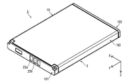
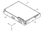
- FIG. 1 is a perspective view showing one appearance of a battery pack according to Embodiment 1.
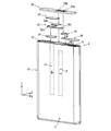
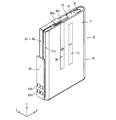
- FIG. 1 is a perspective view showing a core pack 2 of a battery pack 1 according to Embodiment 1.
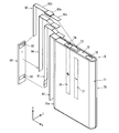
- FIG. 2 is an exploded perspective view of a core pack 2.
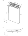
- FIG. (A) is a perspective view which shows the internal structure of the unit cell 10
- (b) is a schematic sectional drawing.
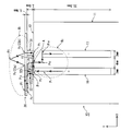
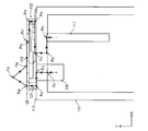
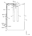
- FIG. 3 is a diagram in which a current path in the battery pack 1 is projected on an XY plane. It is the figure which projected the current path of the battery pack concerning a prior art on the XY plane.
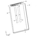
- 3 is a perspective view of a core pack 4 according to a second embodiment.
- FIG. 3 is an exploded perspective view of a core pack 4.
- FIG. 6 is a diagram in which a current path in the battery pack of Embodiment 2 is projected on an XY plane.
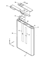
- FIG. 6 is a perspective view showing an appearance of a battery pack 5 according to a third embodiment.
- FIG. 5 is a perspective view of a core pack 6 according to a third embodiment.
- 3 is an exploded perspective view of a core pack 6.
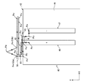
- FIG. 6 is a diagram in which a current path in the battery pack 5 is projected onto an XY plane.
- FIG. 1 is a perspective view illustrating an appearance of a battery pack according to the first embodiment.
- a resin mold 101 is formed so as to cover the circuit board 20 with respect to the core pack 2 to which the circuit board 20 is attached along the upper side of the rectangular unit cell 10, and a bottom plate 102 is provided at the bottom.
- the exterior label 103 is attached and configured so as to cover the entire outer surface of the unit cell 10.
- FIG. 2 is a perspective view of the core pack 2
- FIG. 3 is an exploded perspective view of the core pack 2.
- the unit cell 10 is a flat rectangular lithium ion secondary battery, in which a flat rectangular parallelepiped outer can 11 made of an Al alloy is filled with an electrode body and an electrolyte solution. The opening of the can 11 is formed by being sealed with an exterior lid 12.
- the exterior lid 12 is a long plate extending in the left-right direction, and a negative electrode terminal 13 is protruded at the center of the exterior lid 12, and a positive electrode terminal 14, which is a clad plate, is provided on the right side of the exterior lid 12.
- a safety valve 15 is provided.
- the negative electrode terminal 13 is disposed so as to vertically penetrate a hole formed in the central portion of the exterior lid 12 and is insulated from the exterior lid 12 by a gasket.
- the circuit board 20 is a plate-like component in which an element for forming a protection circuit is built, and an external positive terminal 23a and an external negative terminal 23b for connection are provided on the upper surface thereof.
- the external positive terminal 23 a and the external negative terminal 23 b are exposed to the outside through a window opened in the top surface portion of the resin mold 101.
- the unit cell 10 is disposed on the exterior lid 12 with a gap, and a connection lead plate 31 and a lead pair safety element 32 are interposed between the circuit board 20 and the exterior lid 12.
- the connection lead plate 31 is a U-shaped conductive plate, and connects the positive electrode terminal 14 of the unit cell 10 and the positive electrode conductive land on the lower surface side of the circuit board 20.
- a negative electrode conductive land is provided on the lower surface side of the circuit board 20.
- the lead safety element 32 is configured by joining a lead 32b on the upper surface side of the PTC main body 32a and a lead 32c on the lower surface side.
- the lead 32b rises from the right end of the upper surface of the PTC main body 32a and extends rightward.
- the negative electrode conductive land of the substrate 20 is connected.
- the lead 32 c is connected to the upper part of the negative electrode terminal 13 outside the exterior lid 12. In this way, the negative electrode conductive land of the circuit board 20 is connected to the negative electrode terminal 13 of the unit cell 10 via the lead safety element 32.
- An insulating plate 33 is interposed between the lead safety element 32 and the lower surface of the circuit board 20. Further, an insulating plate 34 is interposed between the lead 32c and the outer lid 12, and an insulating plate 35 is interposed between the right end portion of the circuit board 20 and the outer lid 12, and both are insulated.
- a positive electrode tab 16 extending from the positive electrode plate of the electrode body and a negative electrode tab 17 extending from the negative electrode plate of the electrode body are provided.
- FIG. 4A is a perspective view showing the internal structure of the unit cell 10 in a state where the exterior lid 12 is opened so that the interior can be seen from the opening of the exterior can 11.
- the upper end portion of the positive electrode tab 16 is joined to the back surface of the exterior lid 12, and the upper end portion of the negative electrode tab 17 extends from the lower end portion 13 a of the negative electrode terminal 13 on the back side of the exterior lid 12.
- the lead plate 13b is joined.
- the attachment position of the negative electrode terminal 13 to the exterior cover 12 is located between the connection position of the positive electrode tab 16 to the exterior cover 12 and the connection position of the connection lead plate 31 as the first lead to the exterior cover 12. ing.
- connection lead plate 31 is located immediately above the negative electrode tab 17, and the lead safety element 32, which is the second lead, is located immediately above the positive electrode tab 16.
- lead plate 31 is located immediately above the negative electrode tab 17, and the lead safety element 32, which is the second lead, is located immediately above the positive electrode tab 16.
- Each lead plate and each terminal are joined by resistance spot welding, laser welding, soldering, or the like.
- FIG. 4B is a schematic cross-sectional view showing the positions of the positive electrode tab 16 and the negative electrode tab 17 in the front-rear direction (Z direction) and the left-right direction (Y direction) with respect to the electrode body 18.
- the positive electrode tab 16 is located on the left side, and the negative electrode tab 17 is located on the right side.
- the positive electrode tab 16 and the negative electrode tab 17 are disposed at the center in the front-rear direction (Z direction), but may be disposed closer to the front or rear.
- a through hole penetrating the circuit board 20 is formed at the left end of the circuit board 20.
- the external negative electrode terminal 23b and the upper end of the through hole are connected by printed wiring
- the lower end of the through hole and the negative electrode conductive land are connected by printed wiring.
- FIG. 5 is a diagram in which a current path in the battery pack 1 is projected onto a plane (XY plane) along the positive electrode tab 116 and the negative electrode tab 117 arranged in parallel.
- the current loop starting from the positive electrode plate of the electrode body and returning to the negative electrode plate of the electrode body is represented by points P 1 ⁇ P 2 ⁇ P 3 ⁇ P 4 ⁇ P 5 ⁇ P 6 ⁇ P 7 ⁇ P 8 in the figure.
- the points P1 to P13 indicate the following positions. Top of P1 positive tab 16 Connection portion between P2 positive electrode tab 16 and outer cover 12 Connection portion between P3 connection lead plate 31 and exterior lid 12 P4 External positive terminal 23a P5 External load P6 External negative terminal 23b P7 Upper end of through-hole penetrating circuit board 20 P8 Lower end of through hole penetrating circuit board 20 P9 Connection portion between negative electrode conductive land of circuit board 20 and lead 32b P10 Upper end of rising portion of lead 32b Bottom surface of P11 PTC body 32a P12 Upper end of negative terminal 13 P13 Lower end of negative terminal 13 P14 Upper end of negative electrode tab 17 In the wiring path forming this current loop, the path from the positive electrode tab 16 to the external positive terminal 23a via the outer lid 12 and the circuit board 20 (path connecting the points P1-P2-P3-P4) is the first wiring.
- the path connecting P6 is the second wiring path.
- the attachment position of the negative electrode terminal 13 to the exterior cover 12 is the connection position of the positive electrode tab 16 to the exterior cover 12 and the connection position of the connection lead plate 31 that is the first lead to the exterior cover 12. Since the first wiring path and the second wiring path pass through the exterior lid 12 at the upper end of the unit cell 10, the line connecting the point P2-point P3 and the point P12- The line connecting the points P13 intersects. In FIG. 5, point A is an intersection.
- the current loop is formed inside the unit cell 10 via the intersection A and the current loop part B1 formed via the circuit board 20 outside the unit cell 10 starting from the intersection A.
- the current loop portion B2 is considered separately.
- the current loop portion B1 formed outside the unit cell 10 returns from the point A to the intersection A via the points P3 ⁇ P4 ⁇ P5 ⁇ P6 ⁇ P7 ⁇ P8 ⁇ P9 ⁇ P10 ⁇ P11 ⁇ P12.
- the current loop portion B2 formed in the unit cell 10 includes a current path from the positive electrode tab 16 via the points P1 and P2 to the intersection A, and a negative electrode via the points A and P13 and P14. The current path to the tab 17 is connected.
- the current loop portion B1 is clockwise when viewed from the front, and the current loop portion B2 is counterclockwise when viewed from the front. As described above, the direction in which the current loop portion B1 formed via the circuit board 20 turns outside the unit cell 10 is opposite to the direction in which the current loop portion B2 formed inside the unit cell 10 turns. Therefore, in the place close to the intersection A, the reverse magnetic fields formed by the current loop portions B1 and B2 are canceled.
- connection lead plate 31 as the first lead is located immediately above the negative electrode tab 17, the path portion of the points P3-P4 and the path portion below the point P14 are close to each other, and the current The direction is the reverse direction, and the reverse magnetic field formed by these parts is canceled out.
- lead safety element 32 as the second lead is also located immediately above the positive electrode tab 16, the path portion of the points P1-P2 and the path portion of the points P10-P11 are close to each other, and the current direction Is in the opposite direction, and the reverse magnetic field formed in these parts is canceled out. For this reason, the generated magnetic field can be further reduced.
- FIG. 6 is a diagram in which the current loop of the battery pack according to the comparative example is projected onto the XY plane. As shown in this figure, this current loop goes from the positive electrode tab to the negative electrode tab through the points P21 ⁇ P22 ⁇ P23 ⁇ P24 ⁇ P25 ⁇ P26 ⁇ P27 ⁇ P28 ⁇ P29 ⁇ P30 ⁇ P31 ⁇ P32 ⁇ P33. I'm back.
- the points P21 to P33 indicate the following positions. Top of P21 positive tab P22 Connection between positive electrode tab and outer lid P23 Connection between lead plate and outer lid P24 positive terminal P25 External load P26 negative terminal P27 Upper end of through-hole penetrating circuit board P28 Lower end of through hole penetrating circuit board P29 Connection part between connection lead plate and conductive land of circuit board P30 Connection between lead plate and PTC element P31 Upper end of negative terminal P32 Bent part of negative lead plate P33 Connection between negative electrode tab and negative electrode lead plate The projected current loops do not intersect but form a ring from the inside of the unit cell to the external circuit board. The direction of rotation of the current loop is clockwise when viewed from the front.
- FIG. 7 is a perspective view of the core pack 4 according to the third embodiment
- FIG. 8 is an exploded perspective view of the core pack 4.
- the battery pack according to the present embodiment has the same configuration as that of the battery pack 1 according to the first embodiment.
- the external positive electrode terminal 53 a is connected from the positive electrode tab 46 through the exterior lid 42 and the circuit board 50.
- the first wiring path that reaches the external negative terminal 43 through the outer lid 42 from the negative electrode tab 47 and the second wiring path that reaches the external negative terminal 53b via the circuit board 50 do not cross each other.
- the distance between the first wiring path and the second wiring path passing through the exterior lid 42 and reaching the circuit board 50 is determined by the gap W between the first wiring path and the second wiring path on the inner surface side of the exterior lid 42. Is also narrower.
- the unit cell 40 in the core pack 4 has the same configuration as that of the unit cell 10 according to the first embodiment.
- the negative electrode terminal 43 protrudes from the center of the outer cover 42 and the safety valve 45 is provided at the right end.
- the positive electrode terminal 44 which is a clad plate is provided on the left side of the negative electrode terminal 43.
- the outer can 41 of the unit cell 40 is provided with a positive electrode tab 46 extending from the positive electrode plate of the electrode body and a negative electrode tab 47 extending from the negative electrode plate of the electrode body. ing. 7 and 8, the positive electrode tab 46 and the negative electrode tab 47 extend in the vertical direction (Y direction) and are arranged side by side in the horizontal direction (X direction). Tab 47 is located on the right side.
- the upper end portion of the positive electrode tab 46 is bonded to the back surface of the outer lid 42, and the upper end portion of the negative electrode tab 47 is bonded to a lead plate extended from the lower end portion of the negative electrode terminal 43.
- the circuit board 50 has the same configuration as that of the circuit board 20 of the first embodiment, and has an external positive electrode terminal 53a and an external negative electrode terminal 53b for external connection disposed on the upper surface, and on the outer cover 42 of the unit cell 40. Although arranged at intervals, on the lower surface of the circuit board 50, the position of the positive electrode conductive land is at the left end, and the position of the negative electrode conductive land is at the right end.
- connection lead plate 61 that forms a part of the first wiring path, a safety element 62 with a lead that forms a part of the second wiring path, and the like are interposed.
- the connection lead plate 61 is a first lead member that spans the outer lid 42 and the circuit board 50, and connects the positive terminal 44 of the unit cell 40 and the positive electrode conductive land on the lower surface of the circuit board 50. This is a conductive plate.
- the lead safety element 62 is a second lead member that spans the outer lid 42 and the circuit board 50.
- the lead safety element 62 has a lead 62b bonded to the upper surface side of the PTC body 62a and a lead 62c bonded to the lower surface side. Configured.
- the lead 62c has a tip connected to the negative electrode terminal 43 of the unit cell 40, and the lead 62b is bent in a U shape and connected to the negative electrode conductive land of the circuit board 50.
- the negative electrode conductive land of the circuit board 50 is connected to the negative electrode terminal 43 of the unit cell 40 via the lead safety element 62.
- the lead 62c extends from the negative electrode terminal 43 to the connection lead plate 61 side (left direction).
- the lead 62b further extends to the connection lead plate 61 side (left direction), bends in a U-shape, extends rightward, and reaches the negative electrode conductive land.
- the safety element 62 with lead extends in a direction approaching the connection lead plate 61 in the middle from the negative electrode terminal 43 to the negative electrode conductive land of the circuit board 50, and the safety element 62 with lead and the connection lead plate 61 are close to each other. Therefore, as described below, the area of the current loop portion outside the unit cell 40 is reduced, and the generated magnetic field is also weakened.
- FIG. 9 is a diagram in which the current path in the battery pack according to the second embodiment is projected onto the XY plane.
- the current path passes through points P41 ⁇ P42 ⁇ P43 ⁇ P44 ⁇ P45 ⁇ P46 ⁇ P47 ⁇ P48 ⁇ P49 ⁇ P50 ⁇ P51 ⁇ P52 ⁇ P53 ⁇ P54 in the figure.
- the points P41 to P54 indicate the following positions.
- -P48-P47-P46) is the second wiring path.
- the portion from the passage through the outer lid 42 in the first wiring path to the circuit board 50 (the line portion connecting the points P43 to P44) and the outer lid 42 in the second wiring path.
- the distance from the first part to the circuit board 50 (the line part connecting the points P51 to P50) is narrower than the gap W between the first wiring path and the second wiring path on the inner surface side of the outer lid 42.
- the gap W corresponds to the gap between the upper end of the positive electrode tab 46 and the lower end of the negative electrode terminal 43, and is narrower than the gap between the positive electrode tab 46 and the negative electrode tab 47.
- the bent portions of the connection lead plate 61 and the lead 62b of the safety element 62 with lead are both present on the left side of the negative electrode terminal 43 and are close to each other.
- the path portion connecting the points P50 to P51 of the lead 62b of the safety element 62 with lead are parallel to each other. In this way, the current paths are formed close to each other and parallel to each other in the reverse direction, so that the generated reverse magnetic field is canceled out.
- the path portions formed on the circuit board 50 are also close to each other and parallel to each other in the opposite direction. That is, a route portion along the upper surface of the circuit board 50 (a route portion connecting the points P46 and P47) and a route portion formed by the leads 62b along the lower surface of the circuit board 50 (a route portion connecting the points P49 and P50) , In close proximity to each other and in opposite directions.
- the generated reverse magnetic field is canceled out. Therefore, in the battery pack of this embodiment, the magnetic field generated in the current loop portion outside the unit cell 40 is weak, and the generated magnetic field is weaker than the battery pack according to the comparative example.
- FIG. 10 is a perspective view illustrating an appearance of the battery pack 5 according to the third embodiment.
- FIG. 11 is a perspective view of the core pack 6, and
- FIG. 12 is an exploded perspective view of the core pack 6.
- the circuit board 80 is attached to the side of the rectangular unit cell 70 to form the core pack 6, and the core pack 6 covers the circuit board 80 and the connection leads.
- the resin mold 104 is formed, the bottom plate 105 is attached to the bottom, and the exterior label 106 is attached so as to cover the outer surface of the unit cell 70.
- the first wiring path from the positive electrode tab 76 to the external positive electrode terminal 83a via the outer cover 72 and the circuit board 80, and the negative electrode tab 77 to the outer package passes through the outer lid 72 rather than the inner surface side of the outer lid 72.
- the area reaching the circuit board 80 is narrower.
- the unit cell 70 has the same configuration as that of the unit cell 40 according to the second embodiment.
- a negative electrode terminal 73 protrudes from the center of the outer lid 72 and a safety valve 75 is provided at the right end.
- the positive electrode is a clad plate.
- a terminal 74 is provided on the left side of the negative electrode terminal 73.
- a positive electrode tab 76 extending from the positive electrode plate of the electrode body and a negative electrode tab 77 extending from the negative electrode plate of the electrode body are provided in the outer can 71 of the unit cell 70.
- the positive electrode tab 76 and the negative electrode tab 77 extend in the vertical direction (Y direction) and are arranged side by side in the left and right direction (X direction). Tab 77 is located on the right side.
- the circuit board 80 has the same configuration as that of the circuit board 50 according to the second embodiment, and has an external positive electrode terminal 83a and an external negative electrode terminal 83b for external connection on the surface, and the left side of the outer can 71 of the unit cell 70. It arrange
- On the back surface of the circuit board 80 there is a positive electrode conductive land 81 at the lower end and a negative electrode conductive land 82 at the upper end.
- a connection lead plate 91, a lead safety element 92, and insulating plates 93 and 94 are stacked on the left side 71 a of the outer can 71 and the surface of the outer lid 72.
- the connection lead plate 91 is a first lead member that forms a part of the first wiring path, and is made of a conductive plate bent in an L shape.
- the connection lead plate 91 passes through the left side surface 71a of the outer can 71 and passes through the element.
- the battery 70 is disposed across the positive electrode terminal 74 of the battery 70 and the positive electrode conductive land 81 on the back surface of the circuit board 80, and connects the two.
- the lead safety element 92 is a second lead member that forms a part of the second wiring path.
- the lead 92b is joined to the upper surface side of the PTC main body 92a and the lead 92c is joined to the lower surface side. Connected to the negative electrode terminal 73 of the unit cell 70, the lead 92 b is bent in an L shape and the tip thereof is connected to the negative electrode conductive land 82 of the circuit board 80.
- the lead safety element 92 is arranged across the negative electrode terminal 73 of the unit cell 70 and the negative electrode conductive land 82 of the circuit board 80 and connects the two.
- the insulating plate 93 is bent in an L shape and is interposed between the connection lead plate 91 and the outer can 71 and the outer lid 72 to insulate them.
- the insulating plate 94 is also bent in an L shape, and is interposed between the lead plate 91 and the lead safety element 92 to insulate them.
- the insulating plates 93 and 94 are insulating paper having a thickness of about 0.15 mm. As described above, the insulating plates 93 and 94 are inserted, so that the interval between the first wiring path and the second wiring path is 0.15 mm or more, and the space between the first wiring path and the second wiring path is good. Insulated.
- FIG. 13 is a diagram in which the current path in the battery pack 5 is projected onto the XY plane. The current path passes through points P61 ⁇ P62 ⁇ P63 ⁇ P64 ⁇ P65 ⁇ P66 ⁇ P67 ⁇ P68 ⁇ P69 ⁇ P70 ⁇ P71 ⁇ P72 ⁇ P73 in the figure.
- the points P61 to P74 indicate the following positions. Top of P61 positive electrode tab 76 P62 Connection between positive electrode tab 76 and outer lid 72 P63 Bent part of connection lead plate 91 P64 Positive electrode conductive land 81 P65 External positive terminal 83a P66 External load P67 External negative terminal 83b P68 Through hole that penetrates the circuit board 80 P69 Connection portion between lead 92b and negative electrode conductive land 82 P70 bent part of lead 92b P71 Upper end of negative terminal 73 P72 Bent part of negative electrode lead plate P73 Connection between negative electrode tab 77 and negative lead plate In the wiring path that forms this current loop, a path (points P61-P62-P63-P64-P65 from the positive electrode tab 76 to the external positive electrode terminal 83a via the outer lid 72, the connection lead plate 91, and the circuit board 80 is connected.
- the first wiring path is a path (points P73 to P72) from the negative electrode tab 77 to the external negative electrode terminal 83b through the negative electrode terminal 73, the lead safety element 92, and the circuit board 80.
- -P71-P70-P69-P68-P67) is the second wiring path.
- the portion of the first wiring path from the passage through the outer lid 42 to the circuit board 80 (the path portion connecting the points P62-P63-P64 formed by the connection lead plate 91) and the second wiring
- the distance between the portion of the road from the passage through the exterior lid 42 to the circuit board 80 (the portion connecting the points P69-P70-P71 formed by the lead safety element 92) is the inner surface of the exterior lid 42. It is narrower than the gap W between the first wiring path and the second wiring path. Therefore, the reverse magnetic field generated in these path portions is canceled out.
- the gap W corresponds to the gap between the upper end of the positive electrode tab 76 and the lower end of the negative electrode terminal 73, and is narrower than the gap between the positive electrode tab 76 and the negative electrode tab 77.
- a path portion along the circuit board 80 in the first wiring path (path part connecting the points P63 to P64) and a path part from the external negative terminal 83b on the circuit board 80 to the negative electrode conductive land 82 (point P67- The path portion connecting P68 and P69) is also parallel and close to each other, and the current directions are opposite to each other. Accordingly, the reverse magnetic field generated in these path portions is also canceled.
- a current path is formed outside the unit cell 70 so that the directions of the currents are parallel to each other in the state of being close to each other, and the generated reverse magnetic field is canceled.
- the strength of the magnetic field generated in the current loop portion outside the unit cell 70 is weakened.
- the magnetic field intensity for each direction of X direction, Y direction, and Z direction The components (Bx, By, Bz) were measured.
- the specifications such as the outer can of the unit cell, the electrode body, the positive electrode tab, and the negative electrode tab are common, and the current value is also common.
- Table 1 shows the magnetic field strength (dB) at the location where the positive magnetic field showed the maximum strength and the location where the reverse magnetic field showed the maximum strength for each of the X, Y and Z directions.
- the outer cover of the unit cell is positive, and the negative electrode terminal penetrates the outer cover. Conversely, the outer cover of the unit cell is negative and the outer cover is connected to the positive terminal.
- the negative electrode tab is connected to the exterior lid, and the positive electrode tab is connected to the positive electrode terminal.
- the case where the unit cell built into the battery pack is a lithium ion battery has been described as an example.
- the type of the unit cell built into the battery pack is not particularly limited, and is rectangular.
- the alkaline battery may be used.
- the present invention is suitable for a battery pack for a portable electronic device, particularly a battery pack having a square unit cell.
Landscapes
- Chemical & Material Sciences (AREA)
- Chemical Kinetics & Catalysis (AREA)
- Electrochemistry (AREA)
- General Chemical & Material Sciences (AREA)
- Engineering & Computer Science (AREA)
- Microelectronics & Electronic Packaging (AREA)
- Manufacturing & Machinery (AREA)
- Battery Mounting, Suspending (AREA)
- Connection Of Batteries Or Terminals (AREA)
Abstract
Description
図6は、一般的な角形のリチウムイオン電池を備えたパック電池を示している。
図6に示すパック電池では、回路基板120に保護回路が組み込まれ、回路基板120の外側面には、外部の機器に出力するための外部正極端子(P24)及び外部負極端子(P26)が設けられている。
図6では点P21~点P33を順に結ぶ線で電流ループを示している。
当図に示すように、電極体の正極板から、正極タブ116(P21,P22)、外装蓋112上の正極端子(P23)、回路基板120上の、外部正極端子(P24)及び外部負極端子(P26)、回路基板120の配線(P26~P29)、リード付安全素子132、負極端子113、負極タブ117を経由して電極体の負極板に戻る電流ループが形成される。
そして、この電流ループに鎖交磁束が発生するので、携帯用電子機器にEMI(Electro Magnetic Interference 電磁波障害)が生じ、電気機器が誤動作することもある。
従って、EMIの発生を防止する対策が求められる。特に電池の出力が大きい場合には、鎖交磁束が強くなるので、EMIの発生を防止する対策が必要となる。
ただし、この技術は、複数の電池を備えたパック電池に対して、発生する磁場の強度を低減するのに有効であるが、上記のように1つの角形素電池に回路基板が設けられたパック電池に対しては適用できない。
本発明は、上記課題に鑑み、素電池の外面上に回路基板が設けられたパック電池において、電磁波シールド板などを用いなくてもEMIの発生を抑えることを目的とする。
上記第1形態において、外装蓋を貫通するように、当該外装蓋と絶縁された負極端子を取付け、第1配線路において、正極タブの先端部を外装蓋の内面に接続し、外装蓋と前記回路基板とを、第一リードを介して接続し、負極端子を、正極タブの外装蓋への接続位置と、第一リードの外装蓋への接続位置との間に位置させ、第2配線路において、負極タブを外装蓋の内側で負極端子に接続するとともに、外装蓋の外側で負極端子から回路基板にまたがる第2リード部材を配設することが好ましい。
また、上記目的を達成するため、本発明の第2形態では、有底筒状の外装缶に、正極板と負極板とが積層されてなる電極体が収納され、外装缶内で正極板から延出された正極タブ及び負極板から延出された負極タブが並設され、外装缶の開口部が外装蓋で封止されてなる素電池と、素電池の外面上に配設され、外部に出力する外部正極端子及び外部負極端子が設けられた回路基板と、外装蓋及び回路基板を経由して正極タブと外部正極端子とを結ぶ第1配線路と、外装蓋及び回路基板を経由して負極タブと外部負極端子とを結ぶ第2配線路とを有し、出力時に、正極板から、正極タブ、第1配線路、外部正極端子、外部負極端子、第2配線路、負極タブを順に経由して負極板に戻る電流ループが形成されるパック電池において、第1配線路及び第2配線路の相互の間隔を、外装蓋の内面側よりも、外装蓋を通過してから回路基板に到る箇所でより狭くし、当該箇所で対向して逆向きの電流が流れるようにした。
従って、このパック電池では、遮蔽板などを用いなくても、電流ループによって生じる磁場の強度は、上記従来技術のようなパック電池と比べて低減されることになる。
上記第2形態のパック電池によれば、第1配線路及び第2配線路の相互の間隔を、外装蓋の内面側よりも、外装蓋を通過してから回路基板に到る箇所でより狭くし、当該箇所で対向して逆向きの電流が流れるようになっているので、外装蓋から外部の回路基板にかけて形成される電流ループの面積が小さくなり、電流ループによって生じる磁場の強度が小さくなる。また、対向して逆向きの電流が流れる箇所で磁場が相殺される。
第1配線路及び第2配線路の相互の間隔を絶縁紙などで0.15mm以上確保することによって、第1配線路と第2配線路の間を良好に絶縁することができる。
図1は、実施の形態1にかかるパック電池の外観を示す斜視図である。
このパック電池1は、角形の素電池10の上辺に沿って回路基板20が取付けられてなるコアパック2に対して、回路基板20を覆うように樹脂モールド101が形成され、底部に底板102が装着され、素電池10の外側面全体を被覆するように外装ラベル103が貼り付けられて構成されている。
図2は、コアパック2の斜視図であり、図3はコアパック2の分解斜視図である。
図2,3に示すように、素電池10は、扁平な角形のリチウムイオン二次電池であって、Al合金からなる扁平な直方体形状の外装缶11に電極体および電解液が充填され、外装缶11の開口部が外装蓋12で封口されて形成されている。
負極端子13は、外装蓋12の中央部に開設された孔を上下に貫通するように配設され、外装蓋12とはガスケットによって絶縁されている。
回路基板20は、保護回路を形成するための素子が内蔵された板状部品であって、その上面に、外部に接続用の外部正極端子23aと外部負極端子23bが配設されている。
この外部正極端子23aと外部負極端子23bは、樹脂モールド101の天面部に開設された窓から外部に露出されている。
接続リード板31は、コの字状の導電板であって、素電池10の正極端子14と回路基板20の下面側にある正極導電ランドとを接続している。
回路基板20の下面側には負極導電ランドが設けられている。
このようにして、回路基板20の負極導電ランドは、リード付安全素子32を介して素電池10の負極端子13に接続されている。
この素電池10の外装缶11の中には、電極体の正極板から伸長する正極タブ16及び電極体の負極板から伸長する負極タブ17が設けられている。
図4(a)は、素電池10の内部構造を示す斜視図であって、外装蓋12を開けて外装缶11の開口部から内部が見えるようにした状態の図である。
上記負極端子13の外装蓋12への取付け位置は、正極タブ16の外装蓋12への接続位置と、第1リードである接続リード板31の外装蓋12への接続位置との間に位置している。
なお、各リード板と各端子との接合は、抵抗スポット溶接,レーザー溶接,半田付けなどでなされている。
図4(b)は、正極タブ16及び負極タブ17の電極体18に対する前後方向(Z方向)及び左右方向(Y方向)の位置を示す概略断面図である。
なお、図4(b)に示す例では、正極タブ16及び負極タブ17は、前後方向(Z方向)の中央部に配置されているが、前方寄りあるいは後方寄りに配置されていてもよい。
なお、回路基板20における左端部には、回路基板20を貫通するスルーホールが形成されている。そして、回路基板20の上面において、外部負極端子23bとスルーホールの上端とがプリント配線で接続され、回路基板20の裏面上においてスルーホールの下端と負極導電ランドがプリント配線で接続されている。
図5に示されるように、電極体の正極板から出発して、電極体の負極板に戻ってくる電流ループは、図中の点P1→P2→P3→P4→P5→P6→P7→P8→P9→P10→P11→P12→P13を順に経由している。
P1 正極タブ16の上部
P2 正極タブ16と外装蓋12との接続部分
P3 接続リード板31と外装蓋12との接続部分
P4 外部正極端子23a
P5 外部負荷
P6 外部負極端子23b
P7 回路基板20を貫通するスルーホールの上端
P8 回路基板20を貫通するスルーホールの下端
P9 回路基板20の負極導電ランドとリード32bとの接続部分
P10 リード32bの立ち上がり部分の上端
P11 PTC本体32aの下面
P12 負極端子13の上端部
P13 負極端子13の下端部
P14 負極タブ17の上端部
この電流ループを形成する配線路において、正極タブ16から外装蓋12、回路基板20を経由して外部正極端子23aに到る経路(点P1-P2-P3-P4を結ぶ経路)が第1配線路であり、負極タブ17から外装蓋12を貫く負極端子13及び回路基板20を経由して外部負極端子23bに到る経路(点P14-P13-P12-P11-P10-P9-P8-P7-P6を結ぶ経路)が第2配線路である。
素電池10の外部に形成される電流ループ部分B1は、点Aから点P3→P4→P5→P6→P7→P8→P9→P10→P11→P12を経由して交差点Aに戻るものであり、一方、素電池10内に形成される電流ループ部分B2は、正極タブ16から点P1、点P2を経由して交差点Aに到る電流経路と、交差点Aから点P13,P14を経由して負極タブ17に到る電流経路とをつなぎ合わせたものである。
このように、素電池10の外部において、回路基板20を経由して形成される電流ループ部分B1の回る向きが、素電池10の内部に形成される電流ループ部分B2の回る向きと逆になるので、交差点Aに近い箇所では、各電流ループ部分B1,B2によって形成される逆向きの磁場が相殺される。
(比較例)
図6は比較例にかかるパック電池の電流ループをX-Y面に投影した図である。
当図に示すように、この電流ループは、正極タブから点P21→P22→P23→P24→P25→P26→P27→P28→P29→P30→P31→P32→P33を順に経由して、負極タブに戻っている。
P21 正極タブの上部
P22 正極タブと外装蓋との接続部分
P23 接続リード板と外装蓋との接続部分
P24 正極端子
P25 外部負荷
P26 負極端子
P27 回路基板を貫通するスルーホールの上端
P28 回路基板を貫通するスルーホールの下端
P29 接続リード板と回路基板の導電ランドとの接続部分
P30 接続リード板とPTC素子との接続部分
P31 負極端子の上端部
P32 負極リード板の曲折部
P33 負極タブと負極リード板との接続部分
上記の投影した電流ループは、交差せずに、素電池の内部から外部の回路基板にかけて1つの環を形成している。そして、この電流ループの回転する向きは、前方から見るときに右回りである。
[実施の形態2]
図7は、実施の形態3にかかるコアパック4の斜視図であり、図8はコアパック4の分解斜視図である。
実施の形態1の素電池10と同様に、素電池40の外装缶41の中には、電極体の正極板から伸長する正極タブ46及び電極体の負極板から伸長する負極タブ47が設けられている。図7,8に破線で示されるように、正極タブ46及び負極タブ47は、上下方向(Y方向)に伸長し、左右方向(X方向)に並んで配置され、正極タブ46は左側、負極タブ47は右側に位置している。
回路基板50は、実施の形態1の回路基板20と同様の構成であって、上面に外部接続用の外部正極端子53a外部負極端子53bが配設され、素電池40の外装蓋42の上に間隔をあけて配置されているが、回路基板50の下面において、正極導電ランドの位置は左端部、負極導電ランドの位置は右端部にある。
接続リード板61は、外装蓋42と回路基板50とにまたがる第1リード部材であって、素電池40の正極端子44と回路基板50の下面にある正極導電ランドとを接続するコの字状の導電板である。
このように、リード付安全素子62は、負極端子43から回路基板50の負極導電ランドに到る途中で、接続リード板61に近づく方向に伸び、リード付安全素子62と接続リード板61が近接しているので、下で述べるように、素電池40の外側の電流ループ部分の面積が小さくなり、発生する磁場も弱くなる。
図9は、実施の形態2にかかるパック電池における電流経路をX-Y面に投影した図である。
各点P41~P54は下記の位置を示している。
P41 正極タブ46の上部
P42 正極タブ46と外装蓋42との接続部分
P43 接続リード板61と外装蓋42との接続部分
P44 外部正極端子
P45 外部負荷
P46 外部負極端子
P47 回路基板50を貫通するスルーホールの上端
P48 回路基板50を貫通するスルーホールの下端
P49 リード62bと回路基板50の導電ランドとの接続部分
P50 リード62bの屈曲部上端
P51 リード62bの屈曲部下端
P53 負極端子43の上端部
P54 負極タブ47と負極リード板との接続部分
この電流ループを形成する配線路において、正極タブ46から外装蓋42、接続リード板61,回路基板20を経由して外部正極端子53aに到る経路(点P41-P42-P43-P44を結ぶ経路)が第1配線路であり、負極タブ47から外装蓋42を貫く負極端子43及び回路基板50を経由して外部負極端子53bに到る経路(点P54-P53-P52-P51-P50-P49-P48-P47-P46を結ぶ経路)が第2配線路である。
このように、電流経路が互いに近接した状態で、逆向きで平行になるように形成されているので、発生する逆向きの磁場が相殺される。
すなわち、回路基板50の上面に沿った経路部分(点P46-点P47を結ぶ経路部分)と、回路基板50の下面に沿ったリード62bによる経路部分(点P49-点P50を結ぶ経路部分)は、互いに近接して並行し、向きは逆向きである。
従って、本実施形態のパック電池においては、素電池40の外側の電流ループ部分で発生する磁場は弱く、上記比較例にかかるパック電池と比べると、発生する磁場の強度は弱くなる。
図10は、実施の形態3にかかるパック電池5の外観を示す斜視図である。
図11は、コアパック6の斜視図であり、図12はコアパック6の分解斜視図である。
本実施形態にかかるパック電池5は、角形の素電池70の側辺に回路基板80が取付けられてそのコアパック6が構成され、コアパック6に対して、回路基板80及び接続リードを覆うように樹脂モールド104が形成され、底部に底板105が装着され、素電池70の外側面を被覆するように外装ラベル106が貼り付けられて構成されている。
素電池70は、実施の形態2にかかる素電池40と同様の構成であって、外装蓋72の中央部に負極端子73が凸設され右端部に安全弁75が設けられ、クラッド板である正極端子74が、負極端子73の左側に設けられている。
素電池70の外装缶71の中には、電極体の正極板から伸長する正極タブ76及び電極体の負極板から伸長する負極タブ77が設けられている。図11,12に破線で示されるように、正極タブ76及び負極タブ77は、上下方向(Y方向)に伸長し、左右方向(X方向)に並んで配置され、正極タブ76は左側、負極タブ77は右側に位置している。
外装缶71の左側面71aと外装蓋72の表面上にまたがって、接続リード板91,リード付安全素子92及び絶縁板93,94が積み重ねて配設されている。
リード付安全素子92は、第2配線路の一部を形成する第2リード部材であって、PTC本体92aの上面側にリード92b、下面側にリード92cが接合されて構成され、リード92cは素電池70の負極端子73に接続され、リード92bは、L字状に屈曲されてその先端が回路基板80の負極導電ランド82に接続されている。
絶縁板93は、L字状に曲折され、接続リード板91と、外装缶71及び外装蓋72との間に介挿されて両者を絶縁している。また、絶縁板94もL字状に曲折され、リード板91とリード付安全素子92との間に介挿されて両者を絶縁している。
図13は、パック電池5における電流経路をX-Y面に投影した図である。
電流の経路は、図中の点P61→P62→P63→P64→P65→P66→P67→P68→P69→P70→P71→P72→P73を順に経由している。
P61 正極タブ76の上部
P62 正極タブ76と外装蓋72との接続部分
P63 接続リード板91の曲折部分
P64 正極導電ランド81
P65 外部正極端子83a
P66 外部負荷
P67 外部負極端子83b
P68 回路基板80を貫通するスルーホール
P69 リード92bと負極導電ランド82との接続部分
P70 リード92bの曲折部分
P71 負極端子73の上端部
P72 負極リード板の曲折部
P73 負極タブ77と負極リード板との接続部分
この電流ループを形成する配線路において、正極タブ76から外装蓋72、接続リード板91,回路基板80を経由して外部正極端子83aに到る経路(点P61-P62-P63-P64-P65を結ぶ経路)が第1配線路であり、負極タブ77から外装蓋42を貫く負極端子73、リード付安全素子92及び回路基板80を経由して外部負極端子83bに到る経路(点P73-P72-P71-P70-P69-P68-P67を結ぶ経路)が第2配線路である。
このように、パック電池5においては、素電池70の外部において、互いに近接した状態で並行し電流の向きが互いに逆向きするよう電流経路が形成され、発生する逆向きの磁場が相殺されるので、上記比較例にかかるパック電池と比べると、素電池70の外部における電流ループ部分で発生する磁場の強度は弱くなる。
ここで、実施例1,2及び比較例とも、素電池の外装缶,電極体、正極タブ,負極タブなど仕様は共通とし、電流値も共通とした。

Bx 正向き 素電池の右上部(Q1)
Bx 逆向き 素電池の左上部(Q2)
By 正向き 回路基板の上方(Q3)
By 逆向き 素電池の中央部(Q4)
Bz 正向き 素電池の下端部(Q5)
Bz 逆向き 素電池の上端部(Q6)
表1に示す結果から、実施例1及び実施例2では、比較例と比べて、発生する磁場の強度が低減されていること、特に、実施例1では、磁場が低減される効果が大きいことがわかる。
なお、上記実施の形態1~3では、素電池の外装蓋が正極性で、外装蓋を負極端子が貫通したが、逆に、素電池の外装蓋が負極性で、外装蓋を正極端子が貫通する場合も、同様にして実施可能であって、この場合、負極タブが外装蓋に接続され、正極タブが正極端子に接続される。
2,4,6 コアパック
10 素電池
11 外装缶
12 外装蓋
13 負極端子
13a 下端部
13b リード板
14 正極端子
16 正極タブ
17 負極タブ
20 回路基板
23a 外部正極端子
23b 外部負極端子
31 接続リード板
32 リード付安全素子
32b,32c リード
33,34 絶縁板
40 素電池
41 外装缶
42 外装蓋
43 負極端子
44 正極端子
46 正極タブ
47 負極タブ
50 回路基板
53a 外部正極端子
53b 外部負極端子
61 接続リード板
62 リード付安全素子
62b,62c リード
63 絶縁板
70 素電池
71 外装缶
72 外装蓋
73 負極端子
74 正極端子
76 正極タブ
77 負極タブ
80 回路基板
83a 外部正極端子
83b 外部負極端子
91 接続リード板
92 リード付安全素子
92 安全素子
92a PTC本体
92b,92c リード
93,94 絶縁板
Claims (8)
- 有底筒状の外装缶に、正極板と負極板とが積層されてなる電極体が収納され、前記外装缶内で前記正極板から延出された正極タブ及び前記負極板から延出された負極タブが並設され、前記外装缶の開口部が外装蓋で封止されてなる素電池と、
前記素電池の外面上に配設され、外部に出力する外部正極端子及び外部負極端子が設けられた回路基板と、
前記外装蓋及び前記回路基板を経由して前記正極タブと前記外部正極端子とを結ぶ第1配線路と、
前記回路基板を経由して前記負極タブと前記外部負極端子とを結ぶ第2配線路とを有し、
出力時に、前記正極板から、正極タブ、第1配線路、外部正極端子、外部負極端子、第2配線路、負極タブを順に経由して前記負極板に戻る電流ループが形成されるパック電池であって、
前記併設された正極タブ及び負極タブに沿った平面上に当該電流ループを投影するとき、
前記第1配線路と第2配線路とが、前記外装蓋を通過する箇所において交差し、
当該交差する箇所から素電池の外部に形成される電流ループ部分と、前記交差する箇所から素電池の内部に形成される電流ループ部分とは、電流の回る向きが互いに反対であることを特徴とするパック電池。 - 前記外装缶は角形であり、
前記正極タブ及び前記負極タブは、前記外装缶内で前記外装蓋に向かって延出され、
前記回路基板は、前記外装蓋の外面に沿って間隙をあけて配されていることを特徴とする請求項1記載のパック電池。 - 前記外装蓋を貫通するように、当該外装蓋と絶縁された負極端子が取付けられ、
前記第1配線路において、
前記正極タブが前記外装蓋の内面に接続され、
前記外装蓋と前記回路基板とは、第一リードを介して接続され、
前記負極端子は、前記正極タブの前記外装蓋への接続位置と、前記第一リードの前記外装蓋への接続位置との間に位置しており、
前記第2配線路において、前記負極タブが前記外装蓋の内側で前記負極端子に接続されるとともに、前記外装蓋の外側で前記負極端子から前記回路基板にまたがる第2リード部材が配設されていることを特徴とする請求項2記載のパック電池。 - 前記第一リードは、前記負極タブの直上に位置し、
前記第二リードは、前記正極タブの直上に位置することを特徴とする請求項3記載のパック電池。 - 有底筒状の外装缶に、正極板と負極板とが積層されてなる電極体が収納され、前記外装缶内で前記正極板から延出された正極タブ及び前記負極板から延出された負極タブが並設され、前記外装缶の開口部が外装蓋で封止されてなる素電池と、
前記素電池の外面上に配設され、外部に出力する外部正極端子及び外部負極端子が設けられた回路基板と、
前記外装蓋及び前記回路基板を経由して前記正極タブと前記外部正極端子とを結ぶ第1配線路と、
前記回路基板を経由して前記負極タブと前記外部負極端子とを結ぶ第2配線路とを有し、
出力時に、前記正極板から、正極タブ、第1配線路、外部正極端子、外部負極端子、第2配線路、負極タブを順に経由して前記負極板に戻る電流ループが形成されるパック電池であって、
前記第1配線路及び第2配線路は、
相互の間隔が、前記外装蓋の内面側よりも、前記外装蓋を通過してから前記回路基板に到る箇所でより狭くなっており、当該箇所で対向して逆向きの電流が流れることを特徴とするパック電池。 - 前記外装缶は角形であり、
前記正極タブ及び前記負極タブは、前記外装缶内で前記外装蓋に向かって延出され、
前記回路基板は、前記外装蓋の外面に沿って間隙をあけて配され、
前記外装蓋を貫通するように、当該外装蓋と絶縁された負極端子が取付けられ、
前記第1配線路には、上記外装蓋と回路基板とにまたがる第1リード部材が設けられ、
第2配線路には、前記負極端子と前記回路基板とにまたがる第2リードが設けられ、
前記第2リード部材は、前記負極端子から前記回路基板に到る途中で、前記第1リード部材側方向に伸びていることを特徴とする請求項5記載のパック電池。 - 前記外装缶は角形であり、
前記正極タブ及び前記負極タブは、前記外装缶内で前記外装蓋に向かって延出され、
前記回路基板は、前記外装缶の側辺に沿って配され、
前記外装蓋を貫通するように、当該外装蓋と絶縁された負極端子が取付けられ、
前記第1配線路には、前記外装蓋と回路基板とにまたがる第1リード部材が、外装缶の側辺上を経由して設けられ、
前記第2配線路には、前記負極端子と前記回路基板とにまたがる第2リード部材が、前記第1リード部材に積層されて設けられていることを特徴とする請求項5記載のパック電池。 - 前記第1配線路及び第2配線路の相互の間隔は、
0.15mm以上であることを特徴とする請求項5~7のいずれか記載のパック電池。
Priority Applications (2)
| Application Number | Priority Date | Filing Date | Title |
|---|---|---|---|
| JP2012556812A JP5931756B2 (ja) | 2011-02-08 | 2012-01-17 | パック電池 |
| US13/983,860 US9112244B2 (en) | 2011-02-08 | 2012-01-17 | Battery pack |
Applications Claiming Priority (2)
| Application Number | Priority Date | Filing Date | Title |
|---|---|---|---|
| JP2011024803 | 2011-02-08 | ||
| JP2011-024803 | 2011-02-08 |
Publications (1)
| Publication Number | Publication Date |
|---|---|
| WO2012108233A1 true WO2012108233A1 (ja) | 2012-08-16 |
Family
ID=46638452
Family Applications (1)
| Application Number | Title | Priority Date | Filing Date |
|---|---|---|---|
| PCT/JP2012/050818 Ceased WO2012108233A1 (ja) | 2011-02-08 | 2012-01-17 | パック電池 |
Country Status (3)
| Country | Link |
|---|---|
| US (1) | US9112244B2 (ja) |
| JP (1) | JP5931756B2 (ja) |
| WO (1) | WO2012108233A1 (ja) |
Cited By (1)
| Publication number | Priority date | Publication date | Assignee | Title |
|---|---|---|---|---|
| CN115377619A (zh) * | 2022-08-09 | 2022-11-22 | 合肥国轩高科动力能源有限公司 | 一种双侧出极耳的电芯、电池及装配方法 |
Families Citing this family (4)
| Publication number | Priority date | Publication date | Assignee | Title |
|---|---|---|---|---|
| US10195688B2 (en) | 2015-01-05 | 2019-02-05 | Johnson Controls Technology Company | Laser welding system for a battery module |
| US9893330B2 (en) * | 2016-07-08 | 2018-02-13 | Jiangmen Hongsen Electronic Lighting Co., Ltd. | Battery box body for light-fixture |
| US20230146313A1 (en) * | 2020-03-30 | 2023-05-11 | Sanyo Electric Co., Ltd. | Battery pack for electric bicycle and electric bicycle equipped with battery pack |
| CN112259921B (zh) * | 2020-10-21 | 2025-01-24 | 贵港速博能源科技有限公司 | 一种电池模组的连接电路板 |
Citations (5)
| Publication number | Priority date | Publication date | Assignee | Title |
|---|---|---|---|---|
| JPH03112868U (ja) * | 1990-03-05 | 1991-11-19 | ||
| JP2002100893A (ja) * | 2000-09-21 | 2002-04-05 | Kobe Steel Ltd | 薄型電子装置 |
| JP2003242956A (ja) * | 2002-02-15 | 2003-08-29 | Mitsubishi Electric Corp | バッテリモジュール |
| JP2004103248A (ja) * | 2002-09-04 | 2004-04-02 | Sony Corp | バッテリーパックおよび電磁気ノイズシールドパッチならびに電磁気ノイズシールド方法 |
| JP2004185861A (ja) * | 2002-11-29 | 2004-07-02 | Sony Corp | 回路基板及び電池パック |
Family Cites Families (7)
| Publication number | Priority date | Publication date | Assignee | Title |
|---|---|---|---|---|
| JPH0757715B2 (ja) | 1989-09-26 | 1995-06-21 | 宇部興産株式会社 | 繊維強化炭素質複合材料 |
| JP2007317668A (ja) | 2007-06-11 | 2007-12-06 | Toshiba Corp | 表示機能搭載型電子機器 |
| EP2441105A4 (en) * | 2009-06-10 | 2013-02-27 | Research In Motion Ltd | BATTERY FOR WIRELESS MOBILE COMMUNICATION DEVICE |
| US8357460B2 (en) * | 2009-07-14 | 2013-01-22 | Research In Motion Limited | Low magnetic interference battery and mobile communication device |
| US8642205B2 (en) * | 2010-08-09 | 2014-02-04 | Motorola Mobility Llc | Electrochemical battery pack with reduced magnetic field emission and corresponding devices |
| JP5676620B2 (ja) * | 2010-08-23 | 2015-02-25 | エルジー・ケム・リミテッド | 改良構造のゼリーロールおよびそれを含む二次電池 |
| JP6173692B2 (ja) * | 2010-12-28 | 2017-08-02 | 三洋電機株式会社 | 非水電解質二次電池 |
-
2012
- 2012-01-17 WO PCT/JP2012/050818 patent/WO2012108233A1/ja not_active Ceased
- 2012-01-17 US US13/983,860 patent/US9112244B2/en not_active Ceased
- 2012-01-17 JP JP2012556812A patent/JP5931756B2/ja active Active
Patent Citations (5)
| Publication number | Priority date | Publication date | Assignee | Title |
|---|---|---|---|---|
| JPH03112868U (ja) * | 1990-03-05 | 1991-11-19 | ||
| JP2002100893A (ja) * | 2000-09-21 | 2002-04-05 | Kobe Steel Ltd | 薄型電子装置 |
| JP2003242956A (ja) * | 2002-02-15 | 2003-08-29 | Mitsubishi Electric Corp | バッテリモジュール |
| JP2004103248A (ja) * | 2002-09-04 | 2004-04-02 | Sony Corp | バッテリーパックおよび電磁気ノイズシールドパッチならびに電磁気ノイズシールド方法 |
| JP2004185861A (ja) * | 2002-11-29 | 2004-07-02 | Sony Corp | 回路基板及び電池パック |
Cited By (2)
| Publication number | Priority date | Publication date | Assignee | Title |
|---|---|---|---|---|
| CN115377619A (zh) * | 2022-08-09 | 2022-11-22 | 合肥国轩高科动力能源有限公司 | 一种双侧出极耳的电芯、电池及装配方法 |
| CN115377619B (zh) * | 2022-08-09 | 2024-04-16 | 合肥国轩高科动力能源有限公司 | 一种双侧出极耳的电池及装配方法 |
Also Published As
| Publication number | Publication date |
|---|---|
| JP5931756B2 (ja) | 2016-06-08 |
| JPWO2012108233A1 (ja) | 2014-07-03 |
| US20140004390A1 (en) | 2014-01-02 |
| US9112244B2 (en) | 2015-08-18 |
Similar Documents
| Publication | Publication Date | Title |
|---|---|---|
| JP7111387B2 (ja) | 複合型電流測定装置 | |
| JP6848880B2 (ja) | 蓄電装置 | |
| JP5931756B2 (ja) | パック電池 | |
| JP6098939B2 (ja) | 蓄電モジュール | |
| JP6301480B2 (ja) | 信号収集アセンブリおよび該信号収集アセンブリを備えるパワーバッテリモジュール | |
| JP2018018612A (ja) | 電池用配線モジュール | |
| JP2013187046A (ja) | 組電池 | |
| WO2020100621A1 (ja) | 電池モジュール | |
| US8802263B2 (en) | Battery pack and method of manufacturing the same | |
| JP2010097723A (ja) | 電池パック | |
| US20230261332A1 (en) | Wiring module | |
| JP2015046311A (ja) | 電池パック | |
| JP2023035857A (ja) | 電池モジュール | |
| JP6162459B2 (ja) | 電池パック | |
| JPH1126029A (ja) | 電 池 | |
| JP2014120369A (ja) | 電池パック | |
| JP2019114372A (ja) | 蓄電装置 | |
| JP2011238357A (ja) | 電池 | |
| JP2018026237A (ja) | 配線モジュール | |
| JP2019114540A (ja) | 電池導電接続シート及び電池導電接続モジュール | |
| WO2021084913A1 (ja) | フレキシブルプリント基板、配線モジュール、端子付きフレキシブルプリント基板及び蓄電モジュール | |
| WO2020175201A1 (ja) | 蓄電装置 | |
| JP3909515B2 (ja) | 電池パック | |
| JP2022525464A (ja) | 折り畳み構造を適用したポーチ型バッテリーパック及びその製造方法 | |
| JP2014199722A (ja) | 蓄電装置 |
Legal Events
| Date | Code | Title | Description |
|---|---|---|---|
| 121 | Ep: the epo has been informed by wipo that ep was designated in this application |
Ref document number: 12744625 Country of ref document: EP Kind code of ref document: A1 |
|
| ENP | Entry into the national phase |
Ref document number: 2012556812 Country of ref document: JP Kind code of ref document: A |
|
| NENP | Non-entry into the national phase |
Ref country code: DE |
|
| WWE | Wipo information: entry into national phase |
Ref document number: 13983860 Country of ref document: US |
|
| 122 | Ep: pct application non-entry in european phase |
Ref document number: 12744625 Country of ref document: EP Kind code of ref document: A1 |