WO2012090435A1 - 寸法測定方法及び寸法測定装置 - Google Patents
寸法測定方法及び寸法測定装置 Download PDFInfo
- Publication number
- WO2012090435A1 WO2012090435A1 PCT/JP2011/007114 JP2011007114W WO2012090435A1 WO 2012090435 A1 WO2012090435 A1 WO 2012090435A1 JP 2011007114 W JP2011007114 W JP 2011007114W WO 2012090435 A1 WO2012090435 A1 WO 2012090435A1
- Authority
- WO
- WIPO (PCT)
- Prior art keywords
- substrate
- measured
- dimension
- feature pattern
- pattern
- Prior art date
- Legal status (The legal status is an assumption and is not a legal conclusion. Google has not performed a legal analysis and makes no representation as to the accuracy of the status listed.)
- Ceased
Links
Images







Classifications
-
- G—PHYSICS
- G01—MEASURING; TESTING
- G01B—MEASURING LENGTH, THICKNESS OR SIMILAR LINEAR DIMENSIONS; MEASURING ANGLES; MEASURING AREAS; MEASURING IRREGULARITIES OF SURFACES OR CONTOURS
- G01B11/00—Measuring arrangements characterised by the use of optical techniques
- G01B11/02—Measuring arrangements characterised by the use of optical techniques for measuring length, width or thickness
-
- G—PHYSICS
- G01—MEASURING; TESTING
- G01B—MEASURING LENGTH, THICKNESS OR SIMILAR LINEAR DIMENSIONS; MEASURING ANGLES; MEASURING AREAS; MEASURING IRREGULARITIES OF SURFACES OR CONTOURS
- G01B11/00—Measuring arrangements characterised by the use of optical techniques
- G01B11/16—Measuring arrangements characterised by the use of optical techniques for measuring the deformation in a solid, e.g. optical strain gauge
-
- G—PHYSICS
- G02—OPTICS
- G02F—OPTICAL DEVICES OR ARRANGEMENTS FOR THE CONTROL OF LIGHT BY MODIFICATION OF THE OPTICAL PROPERTIES OF THE MEDIA OF THE ELEMENTS INVOLVED THEREIN; NON-LINEAR OPTICS; FREQUENCY-CHANGING OF LIGHT; OPTICAL LOGIC ELEMENTS; OPTICAL ANALOGUE/DIGITAL CONVERTERS
- G02F1/00—Devices or arrangements for the control of the intensity, colour, phase, polarisation or direction of light arriving from an independent light source, e.g. switching, gating or modulating; Non-linear optics
- G02F1/01—Devices or arrangements for the control of the intensity, colour, phase, polarisation or direction of light arriving from an independent light source, e.g. switching, gating or modulating; Non-linear optics for the control of the intensity, phase, polarisation or colour
- G02F1/13—Devices or arrangements for the control of the intensity, colour, phase, polarisation or direction of light arriving from an independent light source, e.g. switching, gating or modulating; Non-linear optics for the control of the intensity, phase, polarisation or colour based on liquid crystals, e.g. single liquid crystal display cells
- G02F1/1303—Apparatus specially adapted to the manufacture of LCDs
Definitions
- the present invention relates to a dimension measuring method for measuring a dimension of a large substrate to be measured such as a mother substrate of a liquid crystal display device with high accuracy.
- the present invention also relates to a dimension measuring apparatus for measuring the dimension of a large substrate to be measured with high accuracy.
- the liquid crystal display device can be reduced in thickness and has low power consumption, it is widely used as a display for OA devices such as TVs and personal computers, mobile information devices such as mobile phones and PDAs (Personal Digital Assistants).
- OA devices such as TVs and personal computers
- mobile information devices such as mobile phones and PDAs (Personal Digital Assistants).
- the liquid crystal display device includes a liquid crystal display panel and a backlight unit attached to the back side thereof.
- a liquid crystal display panel is disposed opposite to a TFT substrate including a switching element such as a thin film transistor (TFT) and a red (R), green (G), and blue (B).
- the counter substrate includes three color filter layers and a liquid crystal layer formed between the two substrates. And this liquid crystal display device adjusts the transmittance of light incident from the backlight for each pixel by utilizing the fact that the alignment state of the liquid crystal molecules changes by turning on and off the electrode corresponding to the pixel, The transmitted light is transmitted through the colored portion of the color filter layer to perform color display.
- the TFT provided on the TFT substrate is configured by laminating a gate electrode, a semiconductor film, a source electrode and a drain electrode in a predetermined layout.
- the TFT substrate is formed on the substrate main body on each signal line including a gate electrode, a gate insulating film, a semiconductor film, each signal line including a source electrode and a drain electrode, an overcoat film, a planarizing film, a pixel electrode, and an alignment film.
- each signal line including a gate electrode, a gate insulating film, a semiconductor film, each signal line including a source electrode and a drain electrode, an overcoat film, a planarizing film, a pixel electrode, and an alignment film.
- the metal thin film is generally formed by sputtering in a heated environment.
- a Cu film 131 having a thickness of about 5000 mm is formed on the entire surface of the substrate at a high temperature of about 170 ° C. Form.
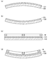
- the temperature of the Cu film decreases after the Cu film is formed, as shown in FIG. 19B, the Cu contracts and the volume of the Cu film 131 decreases, and the substrate 130 warps with the Cu film forming side inward. Bend in the direction.
- the substrate 130 is processed in a state in which it is adsorbed to the entire surface, so that the substrate 130 becomes flat again as shown in FIG.
- the substrate 130 is bent again in a warping direction with the Cu film formation side inside as shown in FIG. 19D.
- the position of the cross mark 140 is measured by detecting the position of the cross mark 140 provided at the four corners of the substrate (pattern matching correction). ). If a cross-shaped object having a predetermined width is provided as the cross mark 140, for example, as shown in FIG. 20, the positions of the eight sides 140a to 140h constituting the cross shape of the cross mark 140 are detected. Then, the coordinates of the center point of the cross mark 140 are calculated from the coordinates of each side (for example, Patent Document 1).
- noise such as cable debris in which the cable is half-broken, hillocks (irregularities), and foreign matter generated during sputtering is present in the detection region 141. There is. If this noise becomes a white bright spot and it is erroneously detected that it forms part of the cross mark 140, the position of the cross mark 140 cannot be measured accurately.
- An object of the present invention is to measure a dimension of a substrate to be measured with high accuracy while suppressing erroneous detection.
- a feature pattern is detected by image recognition of the substrate to be measured, and the dimension of the substrate to be measured is measured.
- the pattern on the board to be measured that is specified by multiple lines including the line is set as a feature pattern, and after detecting the feature pattern by acquiring image data using the region containing the feature pattern as the detection region, the detected feature pattern.
- the step of calculating the dimension of the substrate to be measured from the positional information is provided.
- the pattern on the measurement substrate specified by a plurality of lines including at least two non-parallel lines is set as a feature pattern and the feature pattern is detected. Even when noise such as a half-cut cable is included, it is possible to suppress erroneous detection of noise as a pattern to be detected, and to increase the accuracy of dimension measurement of the substrate to be measured.
- the feature pattern to be detected becomes a clearer pattern. It is possible to more efficiently suppress erroneous detection of noise as a detection target pattern.
- the characteristic pattern of the dimension measuring method of the present invention is one of the cross-shaped marks. Part.
- the positions of the eight sides constituting the cross shape of the mark are further detected from the position information of the detected feature pattern, and the position information From the above, it is preferable to calculate the dimensions of the substrate to be measured.
- the detection target is configured by a straight line, and the detection region If there is noise, the noise may be erroneously recognized as a detection target pattern.
- a pattern specified by a plurality of lines including a straight line extending in one direction and a straight line extending in a direction orthogonal thereto among the cross-shaped marks is detected as a feature pattern. Therefore, even when noise exists in the detection region, it is possible to suppress erroneous detection of noise as a detection target pattern.
- each of the detection areas for obtaining positional information on the eight sides can be made a narrow area. Since the detection area is narrowed, noise is suppressed from being included in the detection area, and position information on eight sides can be obtained by pattern detection with high accuracy.
- the dimension measuring method of the present invention may be configured by a part of the storage capacitor wiring provided in the peripheral region of the mother substrate.
- the dimension measuring method of the present invention is configured by a part of spare wiring for wiring correction provided in a peripheral region of the mother substrate. Also good.
- the vertical length of the substrate to be measured is 600. This is suitable when the width is ⁇ 2880 mm and the lateral length is 720 to 3130 mm.
- a dimension measuring apparatus measures a dimension of a substrate to be measured in order to analyze deformation of the substrate to be measured, and includes a plurality of lines including at least two non-parallel lines on the substrate to be measured.
- a feature pattern storage means for storing the pattern specified in step 1 as a feature pattern
- an image recognition means for acquiring image data on the surface of the substrate to be measured
- a feature pattern stored in the feature pattern storage means is detected from the acquired image data. It is characterized by comprising a feature pattern detection means and a dimension calculation means for calculating the dimension of the substrate to be measured from the detected position information of the feature pattern.
- the feature pattern storage means stores, as a feature pattern, a pattern on the substrate to be measured that is specified by a plurality of lines including at least two non-parallel lines. Even when noise such as a broken cable is included, it is possible to prevent the feature pattern detection unit from erroneously detecting noise as a pattern to be detected, and to measure the dimension of the substrate to be measured with high accuracy. .
- the dimension measuring method of the present invention since the pattern on the substrate to be measured specified by a plurality of lines including at least two non-parallel lines is set as the feature pattern and this feature pattern is detected, the detection is performed. Even when the area includes noise such as a cable that is partially disconnected, it is possible to suppress erroneous detection of noise as a pattern to be detected, and to increase the accuracy of dimension measurement of the substrate to be measured.
- FIG. 2 is a cross-sectional view taken along line II-II in FIG. It is sectional drawing in the area
- FIG. 2 is a cross-sectional view taken along line II-II in FIG. It is sectional drawing in the area
- It is a schematic plan view which shows a mother board
- It is the schematic of a dimension measuring apparatus. The flowchart of the dimension measuring method is shown. It is a top view which shows the area
- FIG. 1 is a cross-sectional view taken along line II-II in FIG. It is sectional drawing in the area
- FIG. 10 is a schematic plan view showing a mother substrate of Modification 5.
- FIG. 10 is an enlarged plan view showing a main part of spare wiring in a sixth modification. It is a top view which shows the pattern of the secondary detection of the modification 6.
- FIG. 10 is an enlarged plan view showing a main part of spare wiring according to a modified example 7; FIG.
- FIG. 10 is an enlarged plan view showing a main part of a storage capacitor wiring according to Modification 8;
- (A)-(d) is explanatory drawing regarding the deformation
- the liquid crystal display device 1 includes a liquid crystal display panel 10 and a backlight unit (not shown) that is a lighting device disposed to face the liquid crystal display panel 10.
- a TFT substrate 11 which is an active matrix substrate and a counter substrate 12 are arranged to face each other.
- a sealing material 13 is provided in a frame shape at the peripheral portion, whereby the two substrates 11 and 12 are bonded.
- a liquid crystal layer 14 is provided in a region surrounded by the sealing material 13 between both the substrates 11 and 12.
- Each of the TFT substrate 11, the counter substrate 12, the sealing material 13, and the liquid crystal layer 14 generally has a known configuration. As shown in FIG.
- the TFT substrate 11 has a signal line including a gate electrode 22, a signal line including a gate insulating film 23, a semiconductor film 24, a source electrode 25S, and a drain electrode 25D on a substrate body 21.
- the overcoat film 26, the planarization film 27, the pixel electrode 28, and the alignment film (not shown) are sequentially stacked.
- the liquid crystal display panel 10 is manufactured by dividing the mother substrate 30, which is a large substrate, into each display area to obtain a liquid crystal display panel size.
- the mother substrate 30 has a layout in which a plurality of liquid crystal display panels 10 (TFT substrates 11) are arranged.
- TFT substrates 11 liquid crystal display panels 10
- the mother substrate 30 is provided with cross-shaped cross marks 40 at the four corners in a region other than the region to be the liquid crystal display panel 10.
- Each of the cross marks 40 has a width of, for example, about 0.2 mm, and a vertical and horizontal length of about 1 mm.
- the cross mark 40 is formed of the same metal film as the gate electrode 22 of the TFT substrate 11.
- Examples of the metal film constituting the cross mark 40 include a laminated film such as a titanium (Ti) film, a molybdenum (Mo) film, a tantalum (Ta) film, and a copper (Cu) film, and an aluminum (Al) film. Can be mentioned.
- the metal film has a thickness of about 0.2 to 1.0 ⁇ m, for example.
- a mother substrate as a test sample (TS) is manufactured, and the substrate dimensions are measured by using the mother substrate after the formation of the metal film as the substrate to be measured, and the substrate deformation amount is examined.
- the substrate is designed including the substrate deformation data of the test sample (TS), and a mother substrate as the primary sample (ES) is manufactured. Also for the primary sample (ES), the substrate dimensions are measured using the mother substrate after forming the metal film as the substrate to be measured, the amount of deformation of the substrate is examined, and it is confirmed that there is no problem. Make it.
- the substrate to be measured whose dimensions are to be measured is the mother substrate 30 for forming a plurality of TFT substrates 10 as described above.
- the mother substrate 30 is patterned so that signal lines including the gate electrode 22 have a predetermined layout.
- the signal line is formed, for example, by sputtering a metal film on the entire surface of the mother substrate, and then applying a resist and patterning.
- the dimension measuring apparatus 100 includes a stage 110 on which a substrate to be measured is placed, and a microscope unit 120 for recognizing image data on the surface of the substrate to be measured and observing a pattern on the substrate to be measured.
- Image recognition means a slider 130 for moving the microscope unit 120 (in FIG. 5, an upper-axis air slider 132 and a lower-axis air slider 133 supported by a stone surface plate 131), and a control unit 140.
- the control unit 140 stores a feature pattern storage unit 141 that stores a predetermined pattern provided on the substrate to be measured as a feature pattern, and the feature pattern stored in the feature pattern storage unit 141 from the image data acquired by the image recognition unit 120.
- the dimension measuring apparatus 100 may be provided integrally with a photo apparatus or the like for forming a resist pattern on a substrate to be measured.
- the feature pattern 41 is inputted and stored in the feature pattern storage unit 141 of the dimension measuring apparatus 100.
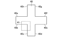
- the feature pattern 41 may be a pattern including a part of the cross mark 40 and a pattern specified by a plurality of lines including two non-parallel lines. Examples of the feature pattern 41 include a pattern specified by a vertical side 40b and a horizontal side 40c (a pattern indicated by a region 41 surrounded by a dotted line in FIG. 7) as shown in FIG.
- step S20 the periphery of the cross mark 40 of the substrate to be measured 30 is photographed using the image recognition unit 120.
- the feature pattern is detected from the image data on the surface of the substrate to be measured using the feature pattern detection unit 142. A pattern that matches the feature pattern 41 stored in the storage unit 141 is detected. At this time, if the detection is successful in step S40, the process proceeds to the next step S50 to calculate the substrate dimensions.
- the pattern specified by the vertical side 40b and the horizontal side 40c is set as the feature pattern 41, there is no possibility of erroneous detection of the feature pattern 41 of the cross mark 40 here.
- the approximate positions of the eight sides 40a to h can be known.
- step S40 If primary detection is not successful in step S40, the feature pattern 41 is changed in step S60, and the process returns to step S10 to perform primary detection again.
- step S50 the substrate dimensions are calculated based on the approximate positions of the eight sides 40a to h found from the detection of the feature pattern 41.
- step S51 secondary detection is performed to check the position coordinates of each of the eight sides 40a to h constituting the cross mark 40.
- step S52 the center point of the cross mark 40 is used by using the dimension calculation means 143.
- the position coordinate of O is calculated.
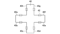
- FIG. 8 shows a detection pattern 42 for performing secondary detection.
- Each of the detection patterns 42 is set so as to straddle each of the eight sides 40a to 40h.
- the area of the detection pattern 42 for detecting the position of each side can be significantly reduced as compared with the prior art.
- each of the detection patterns 42 has a length in a direction orthogonal to each of the eight sides 40a to 40h, for example, 5 to 20 ⁇ m. Since the area of the detection pattern 42 is small, the probability that noise such as a half-broken cable exists in the area of the detection pattern 42 becomes extremely low. As a result, the eight sides 40a to 40h constituting the cross mark 40 with high accuracy. Can be detected.
- the position coordinate of the center point O of the cross mark 40 is calculated from the position coordinate data of the eight sides 40a to h constituting the cross mark 40 obtained by the secondary detection.
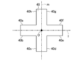
- the straight line l connecting the centers of the sides 40a and 40b and the centers of the sides 40e and 40f, the centers of the sides 40c and 40d, and the centers of the sides 40g and 40h are connected. From the intersection of the straight line m, the coordinates of the center point O of the cross mark 40 are obtained.
- the coordinate axis of the substrate to be measured 30 is determined from the position coordinates of the center point O of each of the cross marks 40 at the four corners.
- the mother substrate 30 of the TFT substrate is obtained.
- the region including two sides of the eight sides of the cross mark is set as the feature pattern.
- the present invention is not limited to this.
- a region including four sides 40a, 40f, 40g, and 40h out of the eight sides 40a to h may be used as the feature pattern 41.
- the mark for measuring the dimension of the substrate to be measured is described as a cross shape having a predetermined width, but other shapes may be used.
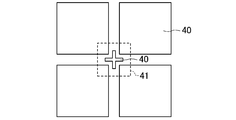
- the marks 40 for measuring the substrate dimensions are arranged in four squares arranged in a matrix at intervals and in the central part of the gaps.
- a pattern including the central cross shape can be used as the feature pattern 41.
- a mark 40 for measuring a substrate dimension includes a square provided with a notch at one corner, and an L-shaped shape facing the notch.
- a pattern including a notch and an L-shape can be used as the feature pattern 41.
- the cross mark is formed of the same metal film as the metal film constituting the gate electrode 22.
- the cross mark may be made of the same metal film as the metal film.
- the cross mark 40 is used when dimension measurement is performed after patterning a signal line including the source electrode 25S and the drain electrode 25D.
- the cross mark made of the same metal film as the metal film constituting the source electrode 25S is, for example, a cross mark rotated by 45 degrees in order to be distinguishable from the cross mark of the gate metal in the steps after the source etching. Provided.
- the cross marks 40 are described as being provided at the four corners of the substrate to be measured 30, but the cross marks 40 may be provided at regions other than the four corners.
- a plurality of cross marks 40 may be provided along a region of the mother substrate 30 that does not become the liquid crystal display panel 10 (TFT substrate 11).
- the mother substrate 30 of the TFT substrate is provided with a wiring such as a spare wiring 50 and a storage capacitor wiring 60 in an area that does not become the liquid crystal display panel 10, and a pattern having a characteristic shape is detected from these wiring patterns. You may measure the dimension of the mother board
- an area including the correction hole 51 provided in the spare wiring 50 may be used as the feature pattern 52 as shown as a sixth modification in FIG.
- the approximate position of the four sides 51a to 51d constituting the correction hole 51 can be known by detecting the feature pattern 52. Therefore, based on the position information of the four sides 51a to 51d.
- a detection pattern 53 is set so as to straddle each of the four sides 51a to 51d, and the position coordinates of the four sides 51a to 51d constituting the correction hole 51 are examined.
- each of the detection patterns 53 has a length in a direction orthogonal to each of the four sides 51a to 51d, for example, 5 to 20 ⁇ m. Since the area of the detection pattern 53 is small, the probability that noise such as a half-broken cable exists in the region of the detection pattern 53 is extremely low, and as a result, the four sides 51a that configure the correction hole 51 with high accuracy. ⁇ D can be detected.
- a pattern including ends of a plurality of storage capacitor wirings 60 is used as a feature pattern, as shown as Modification 8 in FIG. Dimensional measurement may be performed using 61.
- the dimensions of the present invention can be used in the above-described exemplary embodiments and other configurations of Modifications 1 to 8 as long as the pattern is specified by a plurality of lines including two non-parallel lines. It can be used as a feature pattern in the primary detection of measurement.
- the mother substrate 30 of the TFT substrate 11 of the liquid crystal display panel 10 has been described as an example of the substrate to be measured for measuring dimensions.
- the mother substrate of the substrate 12, the mother substrate of the substrate constituting the organic EL display device, the plasma display device or the like may be used as the substrate to be measured, and other substrates other than the mother substrate of the display device may be used as the substrate to be measured. .
- the present invention is useful for a dimension measuring method for measuring a dimension of a substrate to be measured such as a large liquid crystal substrate with high accuracy. Further, the present invention is useful for a dimension measuring apparatus for measuring the dimension of a substrate to be measured such as a large liquid crystal substrate with high accuracy.
- Liquid crystal display device 11 TFT substrate 30 Mother substrate (substrate to be measured) 40 Cross Mark 41 Feature Pattern 50 Preliminary Wiring 52 Feature Pattern 60 Retention Capacitance Wiring 61 Feature Pattern 100 Dimension Measuring Device
Landscapes
- Physics & Mathematics (AREA)
- General Physics & Mathematics (AREA)
- Liquid Crystal (AREA)
Abstract
寸法測定方法は、被測定基板(30)の変形を解析するために被測定基板(30)の画像認識により特徴パターン(41)を検出して被測定基板(30)の寸法を測定するものであって、少なくとも非平行な2本の線を含む複数の線で特定される被測定基板(30)上のパターンを特徴パターン(41)として設定し、特徴パターン(41)を含む領域を検出領域として画像データを取得して特徴パターン(41)を検出した後、検出した特徴パターン(41)の位置情報から被測定基板(30)の寸法を算出する工程を備える。
Description
本発明は、液晶表示装置のマザー基板のような大型の被測定基板の寸法を高精度に測定する寸法測定方法に関する。また、本発明は、大型の被測定基板の寸法を高精度に測定するための寸法測定装置に関する。
液晶表示装置は、薄型化が可能で低消費電力であるため、テレビ、パーソナルコンピュータ等のOA機器や携帯電話、PDA(Personal Digital Assistant)等の携帯情報機器のディスプレイとして広く用いられている。
液晶表示装置は、液晶表示パネルと、その背面側に取り付けられたバックライトユニットとを備えている。液晶表示パネルは、一般に、薄膜トランジスタ(TFT;Thin Film Transistor)等のスイッチング素子を備えたTFT基板と、TFT基板に対向して配置され、赤(R)、緑(G)及び青(B)の3色のカラーフィルタ層が形成された対向基板と、両基板間に形成された液晶層と、で構成されている。そして、この液晶表示装置は、画素に応じた電極をON、OFFすることで液晶分子の配向状態が変わることを利用して、バックライトから入射する光の透過率を画素毎に調整し、その透過光がカラーフィルタ層の着色部分を透過することでカラー表示を行うようになっている。
TFT基板に設けられたTFTは、ゲート電極、半導体膜、ソース電極及びドレイン電極、が所定のレイアウトで積層されて構成されている。
TFT基板は、基板本体上に、ゲート電極を含む各信号線等、ゲート絶縁膜、半導体膜、ソース電極及びドレイン電極を含む各信号線等、オーバーコート膜、平坦化膜、画素電極、配向膜が順に積層された構成を有する。
ところで、金属薄膜は、一般に、加熱された環境下でスパッタリングされることによって成膜される。例えば、銅(Cu)膜131でゲート電極を形成する場合、図19(a)に示すように、まず、170℃程度の高温で、基板上の全面に5000Å程度の厚さのCu膜131を形成する。Cu膜形成後、Cu膜の温度が低下すると、図19(b)に示すように、Cuが収縮してCu膜131の体積が小さくなり、基板130がCu膜形成側が内側になって反る方向に撓む。続いて、マスクMを用いて露光を行うときには、基板130はステージに全面吸着された状態で処理されるため、図19(c)に示すように、基板130は再び平坦となる。露光後、再び基板130の全面吸着を解除すると、これに伴って、図19(d)に示すように、基板130は再びCu膜形成側が内側になって反る方向に撓んでしまう。
この撓みにより、基板寸法にズレが生じ、金属薄膜形成後の製造工程における高精細な設計の妨げとなる問題がある。特に、大型基板を扱う場合には、小さな変形率であっても変形量として大きくなるので、この変形量を正確に測定して把握することが重要となる。
上記説明した基板の撓みによる変形量を調べるために、基板の四隅に設けられた十字形状のマーク140の位置を検出して十字マーク140の位置を測定することが行われている(パターンマッチング補正)。ここで、十字マーク140として、所定幅を有する十字形状の物が設けられている場合、例えば、図20に示すように、十字マーク140の十字形状を構成する8辺140a~hの位置を検出し、各辺の座標から十字マーク140の中心点の座標を算出することが行われる(例えば、特許文献1)。
十字マーク140の十字形状を構成する8辺140a~hを検出する際、検出領域141に、ケーブルが半断線したケーブル屑や、ヒロック(凹凸)、スパッタ時に発生する異物等のノイズが存在することがある。このノイズが白い輝点となり、十字マーク140の一部を構成していると誤検出された場合には、正確に十字マーク140の位置を測定することができなくなる。
本発明は、誤検出を抑制して高精度に被測定基板の寸法の測定を行うことを目的とする。
本発明の寸法測定方法は、被測定基板の変形を解析するために被測定基板の画像認識により特徴パターンを検出して被測定基板の寸法を測定するものであって、少なくとも非平行な2本の線を含む複数の線で特定される被測定基板上のパターンを特徴パターンとして設定し、特徴パターンを含む領域を検出領域として画像データを取得して特徴パターンを検出した後、検出した特徴パターンの位置情報から被測定基板の寸法を算出する工程を備えたことを特徴とする。
上記の寸法測定方法によれば、少なくとも非平行な2本の線を含む複数の線で特定される被測定基板上のパターンを特徴パターンとして設定してこの特徴パターンの検出を行うので、検出領域に半断線したケーブル等のノイズが含まれている場合でも、ノイズを検出対象のパターンとして誤検出してしまうのが抑制され、被測定基板の寸法測定の精度を高めることができる。
本発明の寸法測定方法において、上記特徴パターンを特定する複数の線が一方向に延びる直線、及びそれに直交する方向に延びる直線を含んでいる場合、検出対象となる特徴パターンがよりはっきりしたパターンとなり、ノイズを検出対象のパターンとして誤検出するのをより効率的に抑制することができる。
上記被測定基板が矩形形状を有し、被測定基板の四隅に所定幅を有する十字形状のマークが設けられている場合、本発明の寸法測定方法の特徴パターンは、当該十字形状のマークの一部であってもよい。
この場合、検出した特徴パターンの位置情報から被測定基板の寸法を算出する工程において、検出した特徴パターンの位置情報からさらにマークの十字形状を構成する8辺の位置を検出し、それらの位置情報から上記被測定基板の寸法を算出することが好ましい。
被測定基板の四隅に設けられた十字形状のマークを検出対象とする場合、マークの十字形状を構成する8辺を直接検出の対象とすると、検出対象が直線で構成されることとなり、検出領域にノイズが存在する場合にはノイズを検出対象のパターンと誤認識してしまう虞がある。しかしながら、この発明の寸法測定方法によれば、十字形状のマークのうち、一方向に延びる直線とそれに直交する方向に延びる直線を含む直線を含む複数の線で特定されるパターンを特徴パターンとして検出するので、検出領域にノイズが存在する場合でも、ノイズを検出対象のパターンとして誤検出してしまうのを抑制することができる。
また、特徴パターンの位置情報が得られると、その位置情報に基づいてマークの十字形状を構成する8辺のそれぞれのパターンを検出対象として二次的にパターン検出し、当該8辺の位置情報から被測定基板の寸法を求めることができる。この場合には、特徴パターンの位置と十字形状の8辺の相対的な位置関係が既知であることから、特徴パターンの位置情報から8辺のおよその位置を知ることができる。そのため、二次パターン検出において、8辺の位置情報を得るための検出領域のそれぞれを狭い領域とすることができる。検出領域が狭くなることから、検出領域にノイズが含まれるのが抑制され、高精度でパターン検出により8辺の位置情報を得ることができる。
被測定基板が液晶表示パネルを構成するTFT基板のマザー基板である場合、本発明の寸法測定方法は、マザー基板の周辺領域に設けられた保持容量配線の一部で構成されていてもよい。
被測定基板が液晶表示パネルを構成するTFT基板のマザー基板である場合、本発明の寸法測定方法は、マザー基板の周辺領域に設けられた配線修正用の予備配線の一部で構成されていてもよい。
被測定基板が大型の基板である場合、基板の撓みによる変形量が大きくなるが、本発明によれば、高精度に基板寸法の測定を行うことができるので、被測定基板の縦長さが600~2880mm、及び横長さが720~3130mmである場合に好適である。
本発明の寸法測定装置は、被測定基板の変形を解析するために該被測定基板の寸法を測定するものであって、被測定基板上の少なくとも非平行な2本の線を含む複数の線で特定されるパターンを特徴パターンとして記憶する特徴パターン記憶手段と、被測定基板表面の画像データを取得する画像認識手段と、取得した画像データから、特徴パターン記憶手段で記憶した特徴パターンを検出する特徴パターン検出手段と、検出した特徴パターンの位置情報から被測定基板の寸法を算出する寸法算出手段と、を備えたことを特徴とする。
上記の寸法測定装置によれば、特徴パターン記憶手段は、少なくとも非平行な2本の線を含む複数の線で特定される被測定基板上のパターンを特徴パターンとして記憶するので、検出領域に半断線したケーブル等のノイズが含まれている場合でも、特徴パターン検出手段がノイズを検出対象のパターンとして誤検出してしまうのが抑制され、高精度で被測定基板の寸法測定を行うことができる。
本発明の寸法測定方法によれば、少なくとも非平行な2本の線を含む複数の線で特定される被測定基板上のパターンを特徴パターンとして設定してこの特徴パターンの検出を行うので、検出領域に半断線したケーブル等のノイズが含まれている場合でも、ノイズを検出対象のパターンとして誤検出してしまうのが抑制され、被測定基板の寸法測定の精度を高めることができる。
以下、本発明の実施の形態について、図面を参照して詳細に説明する。
<液晶表示装置>
本実施形態の測定方法について説明する前に、まず、寸法測定の対象となる液晶表示装置について説明する。
本実施形態の測定方法について説明する前に、まず、寸法測定の対象となる液晶表示装置について説明する。
液晶表示装置1は、液晶表示パネル10と、液晶表示パネル10に対向して配置された照明装置であるバックライトユニット(不図示)とを有している。
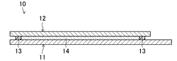
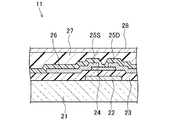
液晶表示パネル10は、図1及び2に示すように、アクティブマトリクス基板であるTFT基板11と、対向基板12とが対向配置されている。両基板11,12の間には、周縁部に枠形状にシール材13が設けられ、これにより両基板11,12が接着されている。両基板11,12間のシール材13に囲まれた領域には、液晶層14が設けられている。TFT基板11、対向基板12、シール材13、液晶層14のそれぞれは、一般に公知の構成を有する。TFT基板11は、図3に示すように、基板本体21上に、ゲート電極22を含む各信号線等、ゲート絶縁膜23、半導体膜24、ソース電極25S及びドレイン電極25Dを含む各信号線等、オーバーコート膜26、平坦化膜27、画素電極28、及び配向膜(不図示)が順に積層された構成を有する。
液晶表示パネル10は、大型基板であるマザー基板30を各表示領域毎に分断して液晶表示パネルサイズにすることにより製造されている。
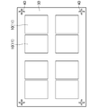
マザー基板30は、図4に示すように、液晶表示パネル10(TFT基板11)が複数枚敷き詰められるように配置されたレイアウトを有する。例えば、縦長さが2880mm程度及び横長さが3130mm程度のサイズのマザー基板30であれば、図4に示すように、60インチ規格の液晶表示パネル10を8枚敷き詰めて配置することができる。マザー基板30は、液晶表示パネル10となる領域以外の領域において、四隅に、十字形状の十字マーク40が設けられている。この十字マーク40のそれぞれは、例えば0.2mm程度の幅を有し、縦横の長さがそれぞれ1mm程度である。十字マーク40は、TFT基板11のゲート電極22と同一の金属膜で形成されている。十字マーク40を構成する金属膜としては、例えば、チタン(Ti)膜、モリブデン(Mo)膜、タンタル(Ta)膜、銅(Cu)膜等のの積層膜や、アルミニウム(Al)膜等が挙げられる。金属膜は、例えば厚さが0.2~1.0μm程度である。
マザー基板30上にゲート電極22等の金属薄膜を形成する際、加熱に伴う熱膨張伸縮や、金属膜の成膜の応力により、2ppm程度の変形が生じる。そのため、この変形量を正確に把握して変形量を考慮した上で、パネルの製造の設計を行う必要がある。そこで、まず初めにテストサンプル(TS)としてのマザー基板を作製し、金属膜形成後におけるマザー基板を被測定基板として基板寸法の測定を行い、基板変形量を調べる。次に、テストサンプル(TS)の基板変形量のデータを含めて基板の設計を行い、1次サンプル(ES)としてのマザー基板を作製する。1次サンプル(ES)についても、金属膜形成後におけるマザー基板を被測定基板として基板寸法の測定を行い、基板変形量を調べ、問題がないことを確認した後、生産用基板(CS)の作製を行う。
<寸法測定方法>
以下、テストサンプル(TS)や1次サンプル(ES)のマザー基板30を被測定基板としてその寸法を測定する方法について、詳細に説明する。
以下、テストサンプル(TS)や1次サンプル(ES)のマザー基板30を被測定基板としてその寸法を測定する方法について、詳細に説明する。
(被測定基板)
寸法を測定する対象となる被測定基板は、本実施形態においては、上記説明したように、TFT基板10を複数形成するためのマザー基板30である。マザー基板30には、ゲート電極22を含む信号線が所定のレイアウトとなるようにパターン形成されている。なお、この信号線は、例えば、金属膜をマザー基板全面にスパッタリングして成膜した後、レジストを塗布してパターンニングして形成される。
寸法を測定する対象となる被測定基板は、本実施形態においては、上記説明したように、TFT基板10を複数形成するためのマザー基板30である。マザー基板30には、ゲート電極22を含む信号線が所定のレイアウトとなるようにパターン形成されている。なお、この信号線は、例えば、金属膜をマザー基板全面にスパッタリングして成膜した後、レジストを塗布してパターンニングして形成される。
(寸法測定装置)
寸法測定装置100は、図5に示すように、被測定基板を載置するステージ110と、被測定基板表面の画像データを認識して被測定基板上のパターンを観察するための顕微鏡部120(画像認識手段)と、顕微鏡部120を移動させるためのスライダー130(図5では、石定盤131により支持された上軸エアースライダー132及び下軸エアースライダー133)と、制御部140と、を有する。制御部140は、被測定基板上に設けられた所定のパターンを特徴パターンとして記憶する特徴パターン記憶手段141と、画像認識手段120によって取得した画像データから特徴パターン記憶手段141で記憶した特徴パターンを検出する特徴パターン検出手段142と、検出した特徴パターンの位置情報から被測定基板の寸法を算出する寸法算出手段143と、を備える。寸法測定装置100は、被測定基板上にレジストパターンを形成するためのフォト装置等と一体に設けられたものであってもよい。
寸法測定装置100は、図5に示すように、被測定基板を載置するステージ110と、被測定基板表面の画像データを認識して被測定基板上のパターンを観察するための顕微鏡部120(画像認識手段)と、顕微鏡部120を移動させるためのスライダー130(図5では、石定盤131により支持された上軸エアースライダー132及び下軸エアースライダー133)と、制御部140と、を有する。制御部140は、被測定基板上に設けられた所定のパターンを特徴パターンとして記憶する特徴パターン記憶手段141と、画像認識手段120によって取得した画像データから特徴パターン記憶手段141で記憶した特徴パターンを検出する特徴パターン検出手段142と、検出した特徴パターンの位置情報から被測定基板の寸法を算出する寸法算出手段143と、を備える。寸法測定装置100は、被測定基板上にレジストパターンを形成するためのフォト装置等と一体に設けられたものであってもよい。
(寸法測定方法)
次に、図6のフローチャートに沿って、被測定基板の寸法測定方法について説明する。
次に、図6のフローチャートに沿って、被測定基板の寸法測定方法について説明する。
-特徴パターン設定-
まず、ステップS10において、寸法測定装置100の特徴パターン記憶手段141に対し、特徴パターン41を入力してこれを記憶させる。特徴パターン41は、十字マーク40の一部を含むパターンであって、非平行な2本の線を含む複数の線で特定されるパターンであればよい。かかる特徴パターン41としては、例えば、図7に示すように、縦の辺40b及び横の辺40cで特定されるパターン(図7における点線で囲まれた領域41で示すパターン)が挙げられる。
まず、ステップS10において、寸法測定装置100の特徴パターン記憶手段141に対し、特徴パターン41を入力してこれを記憶させる。特徴パターン41は、十字マーク40の一部を含むパターンであって、非平行な2本の線を含む複数の線で特定されるパターンであればよい。かかる特徴パターン41としては、例えば、図7に示すように、縦の辺40b及び横の辺40cで特定されるパターン(図7における点線で囲まれた領域41で示すパターン)が挙げられる。
-特徴パターン検出(1次検出)-
次に、ステップS20において、被測定基板30の十字マーク40周辺を画像認識手段120を用いて撮影し、ステップS30において、特徴パターン検出手段142を用いて、被測定基板表面の画像データから特徴パターン記憶手段141に記憶された特徴パターン41と一致するパターンを検出する。このとき、ステップS40において、検出が成功であれば、次のステップS50へ進んで基板寸法算出を行う。
次に、ステップS20において、被測定基板30の十字マーク40周辺を画像認識手段120を用いて撮影し、ステップS30において、特徴パターン検出手段142を用いて、被測定基板表面の画像データから特徴パターン記憶手段141に記憶された特徴パターン41と一致するパターンを検出する。このとき、ステップS40において、検出が成功であれば、次のステップS50へ進んで基板寸法算出を行う。
特徴パターン41としては、縦の辺40b及び横の辺40cで特定されるパターンが設定されているため、ここで十字マーク40の特徴パターン41の誤検出が発生する虞はない。ここで、検出された特徴パターン41と十字マーク40を構成する8辺40a~hとの相対的位置関係から、8辺40a~hのおよその位置が分かる。
なお、ステップS40において、1次検出が成功しなかった場合には、ステップS60において、特徴パターン41を変更して、ステップS10に戻って再度1次検出を行う。
-基板寸法算出-
続いて、ステップS50において、特徴パターン41の検出より分かった8辺40a~hのおよその位置を元にして、基板寸法を算出する。まず、ステップS51において十字マーク40を構成する8辺40a~hのそれぞれの位置座標を調べるための2次検出を行い、その後、ステップS52において、寸法算出手段143を用いて十字マーク40の中心点Oの位置座標を計算する。
続いて、ステップS50において、特徴パターン41の検出より分かった8辺40a~hのおよその位置を元にして、基板寸法を算出する。まず、ステップS51において十字マーク40を構成する8辺40a~hのそれぞれの位置座標を調べるための2次検出を行い、その後、ステップS52において、寸法算出手段143を用いて十字マーク40の中心点Oの位置座標を計算する。
図8は、2次検出を行う検出パターン42を示す。検出パターン42のそれぞれは、8辺40a~hのそれぞれを跨ぐように設定されている。このとき、1次検出において8辺40a~hのそれぞれのおよその位置が分かっているので、各辺の位置を検出するための検出パターン42の面積を従来よりも大幅に小さくすることができる。具体的には、検出パターン42のそれぞれは、8辺40a~hのそれぞれの辺と直交する方向の長さが、例えば5~20μmである。検出パターン42の面積が小さいことにより、検出パターン42の領域内に半断線したケーブル等のノイズが存在する確率が極めて低くなり、結果として、高精度に十字マーク40を構成する8辺40a~hを検出することができる。
次いで、2次検出で得た十字マーク40を構成する8辺40a~hの位置座標のデータより、十字マーク40の中心点Oの位置座標を計算する。図9に示すように、辺40aと辺40bの中心、及び辺40eと辺40fの中心を結んだ直線l、並びに、辺40cと辺40dの中心、及び辺40gと辺40hの中心を結んだ直線mの交点より、十字マーク40の中心点Oの座標が得られる。
最後に、四隅の十字マーク40のそれぞれの中心点Oの位置座標から、被測定基板30の座標軸が決定される。
以上のようにして、被測定基板30の寸法が測定されることにより、被測定基板、ここでは、TFT基板のマザー基板30の変形量についてのデータが得られる。
(変形例)
本実施形態では、十字マークの8辺のうち2辺を含む領域を特徴パターンとして設定するとしたが、特にこれに限られない。例えば、図10に変形例1として示すように、8辺40a~hのうちの4辺40a,40f,40g,40hを含む領域を特徴パターン41としてもよい。
本実施形態では、十字マークの8辺のうち2辺を含む領域を特徴パターンとして設定するとしたが、特にこれに限られない。例えば、図10に変形例1として示すように、8辺40a~hのうちの4辺40a,40f,40g,40hを含む領域を特徴パターン41としてもよい。
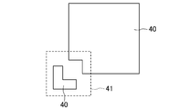
本実施形態では、被測定基板の寸法を測定するためのマークが所定幅を有する十字形状であるとして説明したが、その他の形状であってもよい。例えば、図11に変形例2として示すように、基板寸法を測定するためのマーク40が、互いに間隔をあけてマトリクス状に並べられた4つの正方形と、それらの隙間の中央部分に配置された十字形状と、で構成されていてもよく、この場合、中央の十字形状を含むパターンを特徴パターン41とすることができる。また、図13に変形例3として示すように、基板寸法を測定するためのマーク40が、1隅に切り欠き部が設けられた正方形と、その切り欠き部に対向するL字型の形状と、で構成されていてもよく、この場合、切り欠き部とL字形状とを含むパターンを特徴パターン41とすることができる。
本実施形態では、ゲート電極22を構成する金属膜と同一の金属膜で十字マークが形成されているとして説明したが、例えば、図13に変形例4として示すように、ソース電極25Sを構成する金属膜と同一の金属膜で十字マークが構成されていてもよい。この十字マーク40は、ソース電極25Sやドレイン電極25Dを含む信号線をパターン形成した後に寸法測定を行う場合に用いられる。なお、ソース電極25Sを構成する金属膜と同一の金属膜で構成された十字マークは、ソースエッチング以降の工程においてゲートメタルの十字マークと区別可能にするために、例えば45度回転した十字マークとして設けられる。
本実施形態では、十字マーク40が被測定基板30の四隅に設けられているとして説明したが、十字マーク40が四隅以外の領域に設けられていてもよい。例えば、図14に変形例5として示すように、マザー基板30のうち液晶表示パネル10(TFT基板11)とならない領域に沿って複数の十字マーク40が設けられていてもよい。
また、本実施形態や上記の変形例では、十字マーク40等を用いて寸法測定を行う方法について説明したが、特にこれに限られない。TFT基板のマザー基板30には、液晶表示パネル10とはならない領域に、予備配線50や保持容量配線60等の配線が設けられており、これらの配線パターンのうち特徴的な形状のパターンを検出対象の特徴パターンとしてマザー基板30の寸法測定を行ってもよい。
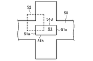
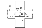
予備配線50の一部を検出対象とする場合、図15に変形例6として示すように、予備配線50に設けられた修正用の孔51を含む領域を特徴パターン52としてもよい。この場合、1次検出において、特徴パターン52を検出することにより修正用の孔51を構成する4辺51a~dのおよその位置が分かるので、当該4辺51a~dの位置情報をもとにして2次検出を行う。2次検出では、図16に示すように、4辺51a~dのそれぞれを跨ぐように検出パターン53を設定し、修正用の孔51を構成する4辺51a~dの位置座標を調べる。このとき、1次検出において4辺51a~dのそれぞれのおよその位置が分かっているので、各辺51a~dの位置を検出するための検出パターン53の面積を従来よりも大幅に小さくすることができる。具体的には、検出パターン53のそれぞれは、4辺51a~dのそれぞれの辺と直交する方向の長さが、例えば5~20μmである。検出パターン53の面積が小さいことにより、検出パターン53の領域内に半断線したケーブル等のノイズが存在する確率が極めて低くなり、結果として、高精度に修正用の孔51を構成する4辺51a~dを検出することができる。
予備配線50の修正用の孔51を寸法測定に用いる場合、図17に変形例7として示すように、予備配線の修正用の孔51を構成する4辺51a~dのうち3辺51b,51c,51dを含む領域を特徴パターン53とすることも可能である。
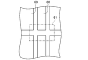
また、保持容量配線60の一部を検出対象とする場合、図18に変形例8として示すように、複数の保持容量配線60(図18では、6つ)の端部を含むパターンを特徴パターン61として用いて寸法測定を行ってもよい。
また、例示的に説明した上記実施形態や変形例1~8の他の構成であっても、非平行な2本の線を含む複数の線で特定されるパターンであれば、本発明の寸法測定の1次検出における特徴パターンとして用いることが可能である。
本実施形態及び上記変形例1~8においては、寸法を測定する被測定基板として、液晶表示パネル10のTFT基板11のマザー基板30について例示的に説明したが、例えば、液晶表示パネル10の対向基板12のマザー基板や、有機EL表示装置、プラズマ表示装置等を構成する基板のマザー基板を被測定基板としてもよく、また、表示装置のマザー基板以外のその他の基板を被測定基板としてもよい。
本発明は、大型の液晶基板のような被測定基板の寸法を高精度に測定する寸法測定方法について有用である。また、本発明は、大型の液晶基板のような被測定基板の寸法を高精度に測定するための寸法測定装置について有用である。
1 液晶表示装置
11 TFT基板
30 マザー基板(被測定基板)
40 十字マーク
41 特徴パターン
50 予備配線
52 特徴パターン
60 保持容量配線
61 特徴パターン
100 寸法測定装置
11 TFT基板
30 マザー基板(被測定基板)
40 十字マーク
41 特徴パターン
50 予備配線
52 特徴パターン
60 保持容量配線
61 特徴パターン
100 寸法測定装置
Claims (8)
- 被測定基板の変形を解析するために被測定基板の画像認識により特徴パターンを検出して該被測定基板の寸法を測定する寸法測定方法であって、
少なくとも非平行な2本の線を含む複数の線で特定される上記被測定基板上のパターンを特徴パターンとして設定し、
特徴パターンを含む領域を検出領域として画像データを取得して特徴パターンを検出した後、
上記検出した特徴パターンの位置情報から上記被測定基板の寸法を算出する
工程を備えたことを特徴とする寸法測定方法。 - 請求項1に記載された寸法測定方法において、
上記非平行な2本の線は、一方向に延びる直線、及びそれに直交する方向に延びる直線であることを特徴とする寸法測定方法。 - 請求項2に記載された寸法測定方法において、
上記被測定基板は矩形形状を有し、
上記特徴パターンは、上記被測定基板の四隅にそれぞれ設けられ、所定幅を有する十字形状のマークの一部であることを特徴とする寸法測定方法。 - 請求項3に記載された寸法測定方法において、
上記検出した特徴パターンの位置情報から上記被測定基板の寸法を算出する工程において、
上記検出した特徴パターンの位置情報からさらに上記マークの十字形状を構成する8辺の位置を検出し、それらの位置情報から上記被測定基板の寸法を算出することを特徴とする寸法測定方法。 - 請求項1または2に記載された寸法測定方法において、
上記被測定基板は、液晶表示パネルを構成する薄膜トランジスタ基板のマザー基板であって、
上記特徴パターンは、被測定基板の周辺領域に設けられた保持容量配線の一部で構成されていることを特徴とする寸法測定方法。 - 請求項1または2に記載された寸法測定方法において、
上記被測定基板は、液晶表示パネルを構成する薄膜トランジスタ基板のマザー基板であって、
上記特徴パターンは、被測定基板の周辺領域に設けられた配線修正用の予備配線の一部で構成されていることを特徴とする寸法測定方法。 - 請求項1~6のいずれかに記載された寸法測定方法において、
上記被測定基板は、縦長さが600~2880mm、及び横長さが720~3130mmであることを特徴とする寸法測定方法。 - 被測定基板の変形を解析するために該被測定基板の寸法を測定する寸法測定装置であって、
被測定基板上の少なくとも非平行な2本の線を含む複数の線で特定されるパターンを特徴パターンとして記憶する特徴パターン記憶手段と、
上記被測定基板表面の画像データを取得する画像認識手段と、
上記取得した画像データから、上記特徴パターン記憶手段で記憶した特徴パターンを検出する特徴パターン検出手段と、
上記検出した特徴パターンの位置情報から上記被測定基板の寸法を算出する寸法算出手段と、
を備えたことを特徴とする寸法測定装置。
Applications Claiming Priority (2)
| Application Number | Priority Date | Filing Date | Title |
|---|---|---|---|
| JP2010-289726 | 2010-12-27 | ||
| JP2010289726 | 2010-12-27 |
Publications (1)
| Publication Number | Publication Date |
|---|---|
| WO2012090435A1 true WO2012090435A1 (ja) | 2012-07-05 |
Family
ID=46382576
Family Applications (1)
| Application Number | Title | Priority Date | Filing Date |
|---|---|---|---|
| PCT/JP2011/007114 Ceased WO2012090435A1 (ja) | 2010-12-27 | 2011-12-20 | 寸法測定方法及び寸法測定装置 |
Country Status (1)
| Country | Link |
|---|---|
| WO (1) | WO2012090435A1 (ja) |
Citations (5)
| Publication number | Priority date | Publication date | Assignee | Title |
|---|---|---|---|---|
| JPH0634325A (ja) * | 1992-07-17 | 1994-02-08 | Hitachi Ltd | 回路基板パターンの寸法計測方法及び装置 |
| JP2006113931A (ja) * | 2004-10-18 | 2006-04-27 | Fujitsu Ltd | 高精度マーク位置・姿勢検出装置 |
| JP2007225522A (ja) * | 2006-02-24 | 2007-09-06 | Shimadzu Corp | 基板の変形量測定方法 |
| JP2008076157A (ja) * | 2006-09-20 | 2008-04-03 | Hitachi Ltd | 寸法測定方法及び寸法測定システム |
| WO2009122529A1 (ja) * | 2008-03-31 | 2009-10-08 | 富士通株式会社 | 面状体のアライメント装置、製造装置、面状体のアライメント方法及び製造方法 |
-
2011
- 2011-12-20 WO PCT/JP2011/007114 patent/WO2012090435A1/ja not_active Ceased
Patent Citations (5)
| Publication number | Priority date | Publication date | Assignee | Title |
|---|---|---|---|---|
| JPH0634325A (ja) * | 1992-07-17 | 1994-02-08 | Hitachi Ltd | 回路基板パターンの寸法計測方法及び装置 |
| JP2006113931A (ja) * | 2004-10-18 | 2006-04-27 | Fujitsu Ltd | 高精度マーク位置・姿勢検出装置 |
| JP2007225522A (ja) * | 2006-02-24 | 2007-09-06 | Shimadzu Corp | 基板の変形量測定方法 |
| JP2008076157A (ja) * | 2006-09-20 | 2008-04-03 | Hitachi Ltd | 寸法測定方法及び寸法測定システム |
| WO2009122529A1 (ja) * | 2008-03-31 | 2009-10-08 | 富士通株式会社 | 面状体のアライメント装置、製造装置、面状体のアライメント方法及び製造方法 |
Similar Documents
| Publication | Publication Date | Title |
|---|---|---|
| CN101872078B (zh) | 液晶显示设备及其制造方法 | |
| US9134615B2 (en) | Exposure method for glass substrate of liquid crystal display | |
| CN103293740B (zh) | 液晶显示面板 | |
| US8704963B2 (en) | Thin film transistor array wherein both an auxiliary electrode and a storage electrode are shaped as an octagonal ring | |
| US9971220B2 (en) | COA substrate and manufacturing method thereof | |
| WO2015068406A1 (ja) | 液晶表示装置 | |
| CN109427661B (zh) | 带对准标记的基板的制造方法 | |
| JP2009192667A (ja) | 表示装置及び表示装置の製造方法 | |
| KR102032962B1 (ko) | 박막 트랜지스터 표시판 및 그 제조 방법 | |
| US8395154B2 (en) | Thin film transistor substrate and method of manufacturing the same | |
| KR101183409B1 (ko) | 액티브 매트릭스 기판, 표시 패널 및 표시 장치 | |
| WO2012090435A1 (ja) | 寸法測定方法及び寸法測定装置 | |
| US20140152909A1 (en) | Touch panel and manufacturing method thereof | |
| JP2006293343A (ja) | 液晶表示装置及び表示装置 | |
| JP5087424B2 (ja) | 半導体装置、及びその寸法測定方法 | |
| US20140168558A1 (en) | Tft array substrate and liquid crystal display | |
| KR101390767B1 (ko) | 표시소자 제조방법 | |
| JP2012185788A (ja) | タッチパネル電極付きカラーフィルタ基板の製造方法とタッチパネル電極付きカラーフィルタ基板、ならびにインナーマーカーを有する透明基板 | |
| CN102736397B (zh) | 光掩模用基板和光掩模及它们的组、制造方法及转印方法 | |
| CN101268415A (zh) | 显示面板用的基板和具有该基板的显示面板 | |
| KR102210607B1 (ko) | 공통 전극의 바이어스 모니터링 영역을 포함하는 박막 트랜지스터 어레이 기판, 그 제조방법 및 이를 이용한 공통 전극의 바이어스 모니터링 방법 | |
| JP2006276747A (ja) | パターン形成方法及び液晶表示装置の製造方法 | |
| KR20070049771A (ko) | 액정표시장치 및 그 제조방법 | |
| KR101577232B1 (ko) | 표시장치의 제조방법 | |
| JP2010032377A (ja) | 測長パターンおよび測長方法 |
Legal Events
| Date | Code | Title | Description |
|---|---|---|---|
| 121 | Ep: the epo has been informed by wipo that ep was designated in this application |
Ref document number: 11854325 Country of ref document: EP Kind code of ref document: A1 |
|
| NENP | Non-entry into the national phase |
Ref country code: DE |
|
| 122 | Ep: pct application non-entry in european phase |
Ref document number: 11854325 Country of ref document: EP Kind code of ref document: A1 |
|
| NENP | Non-entry into the national phase |
Ref country code: JP |