WO2012086516A1 - 表示装置 - Google Patents
表示装置 Download PDFInfo
- Publication number
- WO2012086516A1 WO2012086516A1 PCT/JP2011/079049 JP2011079049W WO2012086516A1 WO 2012086516 A1 WO2012086516 A1 WO 2012086516A1 JP 2011079049 W JP2011079049 W JP 2011079049W WO 2012086516 A1 WO2012086516 A1 WO 2012086516A1
- Authority
- WO
- WIPO (PCT)
- Prior art keywords
- layer
- display device
- color filter
- electrochromic
- light
- Prior art date
- Legal status (The legal status is an assumption and is not a legal conclusion. Google has not performed a legal analysis and makes no representation as to the accuracy of the status listed.)
- Ceased
Links
Images





Classifications
-
- G—PHYSICS
- G02—OPTICS
- G02F—OPTICAL DEVICES OR ARRANGEMENTS FOR THE CONTROL OF LIGHT BY MODIFICATION OF THE OPTICAL PROPERTIES OF THE MEDIA OF THE ELEMENTS INVOLVED THEREIN; NON-LINEAR OPTICS; FREQUENCY-CHANGING OF LIGHT; OPTICAL LOGIC ELEMENTS; OPTICAL ANALOGUE/DIGITAL CONVERTERS
- G02F1/00—Devices or arrangements for the control of the intensity, colour, phase, polarisation or direction of light arriving from an independent light source, e.g. switching, gating or modulating; Non-linear optics
- G02F1/01—Devices or arrangements for the control of the intensity, colour, phase, polarisation or direction of light arriving from an independent light source, e.g. switching, gating or modulating; Non-linear optics for the control of the intensity, phase, polarisation or colour
- G02F1/165—Devices or arrangements for the control of the intensity, colour, phase, polarisation or direction of light arriving from an independent light source, e.g. switching, gating or modulating; Non-linear optics for the control of the intensity, phase, polarisation or colour based on translational movement of particles in a fluid under the influence of an applied field
- G02F1/166—Devices or arrangements for the control of the intensity, colour, phase, polarisation or direction of light arriving from an independent light source, e.g. switching, gating or modulating; Non-linear optics for the control of the intensity, phase, polarisation or colour based on translational movement of particles in a fluid under the influence of an applied field characterised by the electro-optical or magneto-optical effect
- G02F1/167—Devices or arrangements for the control of the intensity, colour, phase, polarisation or direction of light arriving from an independent light source, e.g. switching, gating or modulating; Non-linear optics for the control of the intensity, phase, polarisation or colour based on translational movement of particles in a fluid under the influence of an applied field characterised by the electro-optical or magneto-optical effect by electrophoresis
-
- G—PHYSICS
- G02—OPTICS
- G02B—OPTICAL ELEMENTS, SYSTEMS OR APPARATUS
- G02B26/00—Optical devices or arrangements for the control of light using movable or deformable optical elements
- G02B26/004—Optical devices or arrangements for the control of light using movable or deformable optical elements based on a displacement or a deformation of a fluid
- G02B26/005—Optical devices or arrangements for the control of light using movable or deformable optical elements based on a displacement or a deformation of a fluid based on electrowetting
-
- G—PHYSICS
- G02—OPTICS
- G02F—OPTICAL DEVICES OR ARRANGEMENTS FOR THE CONTROL OF LIGHT BY MODIFICATION OF THE OPTICAL PROPERTIES OF THE MEDIA OF THE ELEMENTS INVOLVED THEREIN; NON-LINEAR OPTICS; FREQUENCY-CHANGING OF LIGHT; OPTICAL LOGIC ELEMENTS; OPTICAL ANALOGUE/DIGITAL CONVERTERS
- G02F1/00—Devices or arrangements for the control of the intensity, colour, phase, polarisation or direction of light arriving from an independent light source, e.g. switching, gating or modulating; Non-linear optics
- G02F1/01—Devices or arrangements for the control of the intensity, colour, phase, polarisation or direction of light arriving from an independent light source, e.g. switching, gating or modulating; Non-linear optics for the control of the intensity, phase, polarisation or colour
- G02F1/13—Devices or arrangements for the control of the intensity, colour, phase, polarisation or direction of light arriving from an independent light source, e.g. switching, gating or modulating; Non-linear optics for the control of the intensity, phase, polarisation or colour based on liquid crystals, e.g. single liquid crystal display cells
- G02F1/133—Constructional arrangements; Operation of liquid crystal cells; Circuit arrangements
- G02F1/1333—Constructional arrangements; Manufacturing methods
- G02F1/1335—Structural association of cells with optical devices, e.g. polarisers or reflectors
- G02F1/133509—Filters, e.g. light shielding masks
- G02F1/133514—Colour filters
-
- G—PHYSICS
- G02—OPTICS
- G02F—OPTICAL DEVICES OR ARRANGEMENTS FOR THE CONTROL OF LIGHT BY MODIFICATION OF THE OPTICAL PROPERTIES OF THE MEDIA OF THE ELEMENTS INVOLVED THEREIN; NON-LINEAR OPTICS; FREQUENCY-CHANGING OF LIGHT; OPTICAL LOGIC ELEMENTS; OPTICAL ANALOGUE/DIGITAL CONVERTERS
- G02F1/00—Devices or arrangements for the control of the intensity, colour, phase, polarisation or direction of light arriving from an independent light source, e.g. switching, gating or modulating; Non-linear optics
- G02F1/01—Devices or arrangements for the control of the intensity, colour, phase, polarisation or direction of light arriving from an independent light source, e.g. switching, gating or modulating; Non-linear optics for the control of the intensity, phase, polarisation or colour
- G02F1/13—Devices or arrangements for the control of the intensity, colour, phase, polarisation or direction of light arriving from an independent light source, e.g. switching, gating or modulating; Non-linear optics for the control of the intensity, phase, polarisation or colour based on liquid crystals, e.g. single liquid crystal display cells
- G02F1/133—Constructional arrangements; Operation of liquid crystal cells; Circuit arrangements
- G02F1/1333—Constructional arrangements; Manufacturing methods
- G02F1/1347—Arrangement of liquid crystal layers or cells in which the final condition of one light beam is achieved by the addition of the effects of two or more layers or cells
- G02F1/13476—Arrangement of liquid crystal layers or cells in which the final condition of one light beam is achieved by the addition of the effects of two or more layers or cells in which at least one liquid crystal cell or layer assumes a scattering state
-
- G—PHYSICS
- G02—OPTICS
- G02F—OPTICAL DEVICES OR ARRANGEMENTS FOR THE CONTROL OF LIGHT BY MODIFICATION OF THE OPTICAL PROPERTIES OF THE MEDIA OF THE ELEMENTS INVOLVED THEREIN; NON-LINEAR OPTICS; FREQUENCY-CHANGING OF LIGHT; OPTICAL LOGIC ELEMENTS; OPTICAL ANALOGUE/DIGITAL CONVERTERS
- G02F1/00—Devices or arrangements for the control of the intensity, colour, phase, polarisation or direction of light arriving from an independent light source, e.g. switching, gating or modulating; Non-linear optics
- G02F1/01—Devices or arrangements for the control of the intensity, colour, phase, polarisation or direction of light arriving from an independent light source, e.g. switching, gating or modulating; Non-linear optics for the control of the intensity, phase, polarisation or colour
- G02F1/15—Devices or arrangements for the control of the intensity, colour, phase, polarisation or direction of light arriving from an independent light source, e.g. switching, gating or modulating; Non-linear optics for the control of the intensity, phase, polarisation or colour based on an electrochromic effect
- G02F1/153—Constructional details
- G02F1/157—Structural association of cells with optical devices, e.g. reflectors or illuminating devices
-
- G—PHYSICS
- G02—OPTICS
- G02F—OPTICAL DEVICES OR ARRANGEMENTS FOR THE CONTROL OF LIGHT BY MODIFICATION OF THE OPTICAL PROPERTIES OF THE MEDIA OF THE ELEMENTS INVOLVED THEREIN; NON-LINEAR OPTICS; FREQUENCY-CHANGING OF LIGHT; OPTICAL LOGIC ELEMENTS; OPTICAL ANALOGUE/DIGITAL CONVERTERS
- G02F1/00—Devices or arrangements for the control of the intensity, colour, phase, polarisation or direction of light arriving from an independent light source, e.g. switching, gating or modulating; Non-linear optics
- G02F1/01—Devices or arrangements for the control of the intensity, colour, phase, polarisation or direction of light arriving from an independent light source, e.g. switching, gating or modulating; Non-linear optics for the control of the intensity, phase, polarisation or colour
- G02F1/13—Devices or arrangements for the control of the intensity, colour, phase, polarisation or direction of light arriving from an independent light source, e.g. switching, gating or modulating; Non-linear optics for the control of the intensity, phase, polarisation or colour based on liquid crystals, e.g. single liquid crystal display cells
- G02F1/133—Constructional arrangements; Operation of liquid crystal cells; Circuit arrangements
- G02F1/1333—Constructional arrangements; Manufacturing methods
- G02F1/1334—Constructional arrangements; Manufacturing methods based on polymer dispersed liquid crystals, e.g. microencapsulated liquid crystals
-
- G—PHYSICS
- G02—OPTICS
- G02F—OPTICAL DEVICES OR ARRANGEMENTS FOR THE CONTROL OF LIGHT BY MODIFICATION OF THE OPTICAL PROPERTIES OF THE MEDIA OF THE ELEMENTS INVOLVED THEREIN; NON-LINEAR OPTICS; FREQUENCY-CHANGING OF LIGHT; OPTICAL LOGIC ELEMENTS; OPTICAL ANALOGUE/DIGITAL CONVERTERS
- G02F1/00—Devices or arrangements for the control of the intensity, colour, phase, polarisation or direction of light arriving from an independent light source, e.g. switching, gating or modulating; Non-linear optics
- G02F1/01—Devices or arrangements for the control of the intensity, colour, phase, polarisation or direction of light arriving from an independent light source, e.g. switching, gating or modulating; Non-linear optics for the control of the intensity, phase, polarisation or colour
- G02F1/13—Devices or arrangements for the control of the intensity, colour, phase, polarisation or direction of light arriving from an independent light source, e.g. switching, gating or modulating; Non-linear optics for the control of the intensity, phase, polarisation or colour based on liquid crystals, e.g. single liquid crystal display cells
- G02F1/133—Constructional arrangements; Operation of liquid crystal cells; Circuit arrangements
- G02F1/1333—Constructional arrangements; Manufacturing methods
- G02F1/1334—Constructional arrangements; Manufacturing methods based on polymer dispersed liquid crystals, e.g. microencapsulated liquid crystals
- G02F1/13345—Network or three-dimensional gels
-
- G—PHYSICS
- G02—OPTICS
- G02F—OPTICAL DEVICES OR ARRANGEMENTS FOR THE CONTROL OF LIGHT BY MODIFICATION OF THE OPTICAL PROPERTIES OF THE MEDIA OF THE ELEMENTS INVOLVED THEREIN; NON-LINEAR OPTICS; FREQUENCY-CHANGING OF LIGHT; OPTICAL LOGIC ELEMENTS; OPTICAL ANALOGUE/DIGITAL CONVERTERS
- G02F1/00—Devices or arrangements for the control of the intensity, colour, phase, polarisation or direction of light arriving from an independent light source, e.g. switching, gating or modulating; Non-linear optics
- G02F1/01—Devices or arrangements for the control of the intensity, colour, phase, polarisation or direction of light arriving from an independent light source, e.g. switching, gating or modulating; Non-linear optics for the control of the intensity, phase, polarisation or colour
- G02F1/13—Devices or arrangements for the control of the intensity, colour, phase, polarisation or direction of light arriving from an independent light source, e.g. switching, gating or modulating; Non-linear optics for the control of the intensity, phase, polarisation or colour based on liquid crystals, e.g. single liquid crystal display cells
- G02F1/133—Constructional arrangements; Operation of liquid crystal cells; Circuit arrangements
- G02F1/1333—Constructional arrangements; Manufacturing methods
- G02F1/1334—Constructional arrangements; Manufacturing methods based on polymer dispersed liquid crystals, e.g. microencapsulated liquid crystals
- G02F1/13347—Constructional arrangements; Manufacturing methods based on polymer dispersed liquid crystals, e.g. microencapsulated liquid crystals working in reverse mode, i.e. clear in the off-state and scattering in the on-state
-
- G—PHYSICS
- G02—OPTICS
- G02F—OPTICAL DEVICES OR ARRANGEMENTS FOR THE CONTROL OF LIGHT BY MODIFICATION OF THE OPTICAL PROPERTIES OF THE MEDIA OF THE ELEMENTS INVOLVED THEREIN; NON-LINEAR OPTICS; FREQUENCY-CHANGING OF LIGHT; OPTICAL LOGIC ELEMENTS; OPTICAL ANALOGUE/DIGITAL CONVERTERS
- G02F1/00—Devices or arrangements for the control of the intensity, colour, phase, polarisation or direction of light arriving from an independent light source, e.g. switching, gating or modulating; Non-linear optics
- G02F1/01—Devices or arrangements for the control of the intensity, colour, phase, polarisation or direction of light arriving from an independent light source, e.g. switching, gating or modulating; Non-linear optics for the control of the intensity, phase, polarisation or colour
- G02F1/13—Devices or arrangements for the control of the intensity, colour, phase, polarisation or direction of light arriving from an independent light source, e.g. switching, gating or modulating; Non-linear optics for the control of the intensity, phase, polarisation or colour based on liquid crystals, e.g. single liquid crystal display cells
- G02F1/133—Constructional arrangements; Operation of liquid crystal cells; Circuit arrangements
- G02F1/135—Liquid crystal cells structurally associated with a photoconducting or a ferro-electric layer, the properties of which can be optically or electrically varied
- G02F1/1351—Light-absorbing or blocking layers
-
- G—PHYSICS
- G02—OPTICS
- G02F—OPTICAL DEVICES OR ARRANGEMENTS FOR THE CONTROL OF LIGHT BY MODIFICATION OF THE OPTICAL PROPERTIES OF THE MEDIA OF THE ELEMENTS INVOLVED THEREIN; NON-LINEAR OPTICS; FREQUENCY-CHANGING OF LIGHT; OPTICAL LOGIC ELEMENTS; OPTICAL ANALOGUE/DIGITAL CONVERTERS
- G02F2201/00—Constructional arrangements not provided for in groups G02F1/00 - G02F7/00
- G02F2201/44—Arrangements combining different electro-active layers, e.g. electrochromic, liquid crystal or electroluminescent layers
-
- G—PHYSICS
- G02—OPTICS
- G02F—OPTICAL DEVICES OR ARRANGEMENTS FOR THE CONTROL OF LIGHT BY MODIFICATION OF THE OPTICAL PROPERTIES OF THE MEDIA OF THE ELEMENTS INVOLVED THEREIN; NON-LINEAR OPTICS; FREQUENCY-CHANGING OF LIGHT; OPTICAL LOGIC ELEMENTS; OPTICAL ANALOGUE/DIGITAL CONVERTERS
- G02F2203/00—Function characteristic
- G02F2203/34—Colour display without the use of colour mosaic filters
-
- G—PHYSICS
- G02—OPTICS
- G02F—OPTICAL DEVICES OR ARRANGEMENTS FOR THE CONTROL OF LIGHT BY MODIFICATION OF THE OPTICAL PROPERTIES OF THE MEDIA OF THE ELEMENTS INVOLVED THEREIN; NON-LINEAR OPTICS; FREQUENCY-CHANGING OF LIGHT; OPTICAL LOGIC ELEMENTS; OPTICAL ANALOGUE/DIGITAL CONVERTERS
- G02F2203/00—Function characteristic
- G02F2203/62—Switchable arrangements whereby the element being usually not switchable
Definitions
- the present invention relates to a display device, and more particularly to a liquid crystal display device.
- the color liquid crystal display devices that are currently widely used are provided with color filters corresponding to the pixels, and typically correspond to the three primary colors of red (R), green (G), and blue (B) light.
- the color filters to be arranged are arranged in a predetermined pattern corresponding to the pixels.
- a color display pixel is composed of a plurality of primary color pixels (typically, three of R, G, and B).
- a liquid crystal layer is formed between a pair of substrates, and the color filter layer in which the plurality of color filters described above are arranged corresponding to pixels is formed on any one of the substrates.
- a liquid crystal layer is formed between a TFT substrate on which circuit elements such as pixel electrodes and TFTs (Thin Film Transistors) are formed and a counter substrate on which a counter electrode and a color filter are formed. Yes.
- the counter substrate having this color filter is often called a color filter substrate.
- liquid crystal display devices including such color filters have low light use efficiency.
- the intensity of light transmitted through the color filter out of the light incident on the color filter is approximately 1/3 (one third) of the intensity of the light incident on the color filter, and the brightness is reduced.
- a reflective liquid crystal display device using external light has a problem that a highly visible color display is obtained in a bright environment, but a highly visible color display is difficult to obtain in a dark environment.
- Patent Documents 1 to 3 disclose a color display device including a color liquid crystal display device for solving these problems.
- the color filter included in the display device disclosed in Patent Document 1 requires an element such as a TFT that drives an electrochromic dye for each pixel, and therefore the aperture ratio of the pixel is reduced. As a result, the light transmittance is reduced, and the visibility of the display image is deteriorated. Further, in order to color the color filter, it is always necessary to supply power, and the power consumption of the display device is increased.
- the present invention has been made in view of the above points, and an object of the present invention is to provide a display device that can obtain a highly visible image and consumes less power.
- a display device has a memory property and is applied between a first substrate and a second substrate disposed so as to face each other, and between the first substrate and the second substrate.
- An active color filter layer that is colored or decolored according to voltage, and the intensity of light incident on the active color filter layer, the degree of scattering, or the light that has passed through the active color filter layer And a light modulation layer for controlling the degree of scattering.
- the active color filter layer is an electrochromic layer.
- the electrochromic layer includes an oxidized electrochromic layer having an oxidized color forming material and a reduced electrochromic layer having a reduced color forming material.
- the color developing material and the reduction-type color forming material have different light absorption wavelengths in the color developing state.
- the oxidized electrochromic layer has a first oxidized electrochromic region having a single oxidized coloring material across two pixels adjacent in the row direction, and the reduced electrochromic layer.
- the chromic layer has a first reduced electrochromic region having a single reduced coloring material across two pixels adjacent in the row direction.
- the oxidized electrochromic layer includes two portions each having an oxidized coloring material having different light absorption wavelengths in a colored state corresponding to two pixels adjacent in the row direction.
- the reduction-type electrochromic layer has a dioxidation-type electrochromic region, and the reduction-type electrochromic layer has reduction-type coloring materials having different light absorption wavelengths in a coloring state corresponding to two pixels adjacent in the row direction.
- a second reduced electrochromic region including two portions, wherein the first oxidized electrochromic region and the second reduced electrochromic region face each other, and the first reduced electrochromic region and the second oxidized The electrochromic layer is formed so as to face the type electrochromic region.
- the active color filter layer is an electrophoretic layer.
- the display device includes a first electrode and a second electrode for applying a voltage to the electrophoretic layer, and the size of the first electrode is smaller than the size of the second electrode.
- the first electrode is formed in a light shielding region of the display device when viewed from the normal direction of the display surface of the display device.
- the display device described above further includes a backlight.
- the display device is a see-through display device.
- the active color filter layer is formed on the side on which strong light is incident among light incident on the see-through display device, rather than the light modulation layer.
- the active color filter layer is formed closer to the viewer than the light modulation layer.
- the active color filter layer is formed on the first substrate side of the light modulation layer, and a further active color filter layer is formed on the second substrate side of the light modulation layer.
- the display device further includes a layer having a conductive polymer or a solid electrolyte, and applies a voltage to the active color filter layer via the layer having the conductive polymer or the solid electrolyte.
- a protective layer is formed on the active color filter layer side or the light modulation layer side of the layer having the conductive polymer or solid electrolyte.
- a transparent electrode is formed on the light modulation layer side of the layer having the conductive polymer or the solid electrolyte, and the protective layer is the active color filter layer side of the transparent electrode, or It is formed on the light modulation layer side.
- the display device described above further includes a protective layer having a first main surface and a second main surface parallel to the first main surface, and the first main surface and the second main surface include: An electrode is formed, and a voltage is applied to the active color filter layer through the electrode on the active color filter layer side among the electrodes.
- the light modulation layer is an electrowetting layer.
- the light modulation layer is a liquid crystal layer.
- the light modulation layer is a scattering type liquid crystal layer.
- the light modulation layer is a PDLC layer or a PNLC layer.
- the display device further includes a color filter layer, and the active color filter layer is formed so as to overlap with the color filter layer when viewed from the normal direction of the display surface of the display device. Yes.
- an image with high visibility is obtained, and a display device with low power consumption is provided.
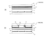
- (A) And (b) is typical sectional drawing of display apparatus 100A1 and 100A2 (100A) in embodiment by this invention. It is typical sectional drawing which shows the modification of the color filter layer used for display apparatus 100A. It is typical sectional drawing which shows the modification of the color filter layer used for display apparatus 100A in embodiment by this invention.
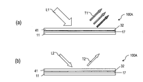
- (A) And (b) is a typical figure explaining the display state of 100 A of display apparatuses.
- (A) And (b) is typical sectional drawing of display apparatus 100B1 and 100B2 (100B) in other embodiment by this invention.
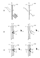
- (A)-(c) is typical sectional drawing of the display apparatus 100B.
- (A) And (b) is typical sectional drawing of display apparatus 100C1 and 100C2 (100C) in further another embodiment by this invention.
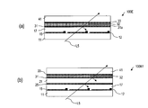
- FIG. 100C It is a schematic diagram explaining the display state of the display device 100C. It is a typical perspective view of display apparatus 100D in further another embodiment by the present invention. (A) And (b) is a typical figure explaining the display state of display apparatus 100D. (A) is typical sectional drawing of display apparatus 100E in further another embodiment by this invention, (b) is typical sectional drawing of display apparatus 100B1 demonstrated in contrast with display apparatus 100E. is there.
- a display device 100A according to an embodiment of the present invention will be described with reference to FIGS.
- the display device 100A is a reflective display device.
- the display devices 100A1 and 100A2 are reflective liquid crystal display devices, and the display device 100A3 is a reflective electrowetting display device.
- FIG. 1A is a schematic cross-sectional view of the display device 100A1.
- a display device 100 ⁇ / b> A ⁇ b> 1 illustrated in FIG. 1A includes a first substrate (for example, a glass substrate) 11, an insulating substrate (for example, a glass substrate) 21 facing the first substrate 11, and between the first substrate 11 and the insulating substrate 21.
- the light modulation layer 17 is provided.
- Transparent electrodes 15 and 25 made of, for example, ITO (Indium ⁇ Tin Oxide) or the like are formed on the first substrate 11 and the insulating substrate 21, respectively.
- the light modulation layer 17 is provided between the transparent electrode 15 and the transparent electrode 25.
- the display device 100A1 includes a second substrate (for example, a glass substrate) 41 facing the opposite side of the insulating substrate 21 from the first substrate 11 side, and a memory provided between the insulating substrate 21 and the second substrate 41. And has a layer (active color filter layer) 32 that is colored or decolored depending on the applied voltage.
- the decolored state refers to a state where the visible light transmittance is 40% or more, and preferably 70% or more.
- An active color filter layer 32 and a light modulation layer 17 are formed between the first substrate 11 and the second substrate 41.
- the light modulation layer 17 is a layer that controls the intensity of light incident on the active color filter layer 32, the degree of scattering, or the intensity of light transmitted through the active color filter layer 32, or the degree of scattering. is there.
- a transparent electrode 31 made of ITO or the like is formed on the side opposite to the light modulation layer 17 side of the insulating substrate 21, and a transparent electrode 33 is similarly formed on the light modulation layer 17 side of the second substrate 41. .
- An active color filter layer 32 is formed between the transparent electrode 31 and the transparent electrode 33.
- An active element 12 such as a TFT is formed on the first substrate 11 for each pixel.
- An insulating layer 13 is formed between the first substrate 11 and the transparent electrode 15.
- the active element 12 is electrically connected to the transparent electrode 15 in a contact hole formed in the insulating layer 13. Further, the light modulation layer 17 may be passively driven without providing the active element 12. At this time, the transparent electrodes 15 and 25 are formed in a stripe shape.
- a reflective plate that reflects visible light is provided on the opposite side of the first substrate 11 of the display device 100A1 from the light modulation layer 17 side. Display can be performed in a reflection mode using light incident from the two-substrate 41 side.
- the display device 100A1 is a liquid crystal display device in an IPS (In-Plain Switching) mode or an FFS (Fringe Field Switching) mode
- the transparent electrode 25 can be omitted.
- the insulating layer 13 can be omitted as appropriate.
- the active color filter layer 32 may be configured to display a variety of colors by forming a plurality of colors (for example, R, G, B) for each pixel as shown in FIG. Alternatively, a single color is arranged uniformly, a single color is formed in a certain area in the display device 100A1, or a plurality of colors are formed separately for each area in the display device 100A1, so that a monocolor or an area color can be formed. You may enable it to display.
- a plurality of colors for example, R, G, B
- the active color filter layer 32 is, for example, a layer (referred to as an electrochromic layer) 32a having an electrochromic material.
- an electrochromic layer 32a having an electrochromic material.
- the absorption wavelength is not the desired absorption wavelength, a plurality of electrochromic layers 32a having different color forming materials may be stacked.
- the electrochromic layer 32a is a layer in which an electrochromic material in an electrolyte solution is oxidized or reduced by application of a voltage to be colored or decolored.
- the electrolyte solution acetonitrile, NMP (1-methyl-2-pyrrolidone), DMSO (dimethyl sulfoxide) or the like is used as a solvent, and TBAP (tetrabutylammonium perchlorate) or TEAP (tetraethylammonium perchlorate) is used as an electrolyte. ) Etc. are used.
- a styryl dye is used as a material that develops color when the electrochromic material is oxidized
- a phthalic acid derivative, viologen, or the like is used as a material that develops color when the electrochromic material is reduced.
- the counter electrode has an effect of promoting oxidation at the electrode facing the electrode contributing to the coloring of the material.
- an electrochromic material has almost no memory property when the electrochromic material is dispersed in a solution. The reason is that when the power supply is stopped, the colored molecules diffuse and are decolored by electron exchange with the counter electrode.
- a method for providing a memory property there is a method in which carboxylic acid, phosphoric acid, or the like is introduced into an electrochromic material as an anchor, and the electrochromic material is adsorbed to fine particles such as titanium oxide or zinc oxide formed on a substrate.
- carboxylic acid, phosphoric acid, or the like is introduced into an electrochromic material as an anchor, and the electrochromic material is adsorbed to fine particles such as titanium oxide or zinc oxide formed on a substrate.
- a method of increasing the viscosity of the electrolytic solution by applying a polymer or the like, or a method of gelation or solidification. These methods have the effect of preventing or reducing the diffusion of the colored electrochromic material.
- a method for forming a plurality of coloring materials separately is, for example, forming fine particles such as titanium oxide on a substrate, and forming an electrochromic material dissolved in a solvent on the fine particles separately for each coloring material by an ink jet device. Is the method.
- the display device 100A1 sets the electrochromic layer 32a in a colored state and performs full color display, monocolor display, or area color display. For example, when it is desired to display only in a dark place or black and white, the electrochromic layer 32a. Can be displayed in a decolored state, and display with high brightness can be performed. For this reason, in a reflective display that does not have a light emitting source and displays using only external light, a color display including color information and a display with high brightness that emphasizes visibility are arbitrarily selected according to the lighting environment. Can be switched to.
- the electrochromic layer 32a has a memory property, power can be suppressed. Saturation and brightness can be arbitrarily adjusted by adjusting the magnitude of the voltage applied to the electrochromic layer 32a.
- the display device 100A2 having the same effect as the display device 100A1 will be described.
- the same referential mark is attached
- FIG. 1B is a schematic cross-sectional view of the display device 100A2.
- the display device 100A2 is a display device in which the electrochromic layer 32a of the display device 100A1 is an electrophoretic layer 32b and the transparent electrode 33 of the display device 100A1 is a transparent electrode 35 formed in a line shape.
- the shape of the transparent electrode 35 is not limited to this.
- the transparent electrode 31 and the transparent electrode 35 have different sizes. For example, the size of the transparent electrode 35 is smaller than the size of the transparent electrode 31.
- an electrode formed from an opaque metal for example, Al (aluminum) may be used.
- the electrophoretic layer 32b has a resin wall 39 between pixels, and has charged colored fine particles 71 containing a pigment or a dye for each pixel.
- charged colored fine particles 71 containing a pigment or a dye for each pixel.
- red, blue and green charged colored fine particles 71 are respectively provided in desired pixels.
- the electrophoretic layer 32b in the middle pixel is in a decolored state in order to make the driving state easy to understand.
- the electrophoretic layer 32b in the other pixels is in a colored state.
- the color intensity of the display device 100A2 can be changed.
- a method of forming the charged colored fine particles 71 separately for each color for example, there is a method of forming the charged colored fine particles 71 dispersed in a solution between the resin walls 39 divided for each color by an ink jet method. Further, when the charged colored fine particles 71 cannot be adjusted to a desired color, a plurality of charged colored fine particles 71 having different colors may be mixed in the same pixel.
- the above-described electrochromic layer 32a may be overlapped with a color filter 23 containing a conventional pigment, for example.
- the electrochromic layer 32a is formed so as to overlap with the color filter 23 when viewed from the display surface of the display device. In this way, the color filter is not switched between color development and color erasure, but display with high color purity is performed when the electrochromic layer 32a is in the color development state, and when the electrochromic layer 32a is in the color erasure state. Display that emphasizes lightness rather than color purity can be performed.
- the electrophoretic layer 32b may be overlapped with a conventional color filter containing a pigment.
- a black matrix formed of metal or resin may be provided between different colors of the electrochromic layer 32a (or electrophoretic layer 32b) or at a position corresponding to, for example, a pixel of the insulating substrate 21.
- a black resin wall may be formed between different colors of the electrochromic layer 32a (or the electrophoretic layer 32b).
- the light modulation layer 17 is, for example, a scattering type liquid crystal layer.
- the light modulation layer 17 is a normal mode PNLC (Polymer-Network-Liquid-Crystal) layer or PDLC (Polymer-Dispersed-Liquid-Crystal) layer that scatters when a low voltage is applied and becomes transparent when a high voltage is applied.
- the light modulation layer 17 is, for example, a liquid crystal layer in which liquid crystal molecules are TN (TwistedistNematic) alignment, parallel alignment or vertical alignment, or a reverse mode PNLC layer that becomes transparent when a low voltage is applied and scatters when a high voltage is applied.
- the light modulation layer 17 may be a liquid or gas electrophoretic layer, an electrowetting (EW) layer, a mechanical shutter layer, or the like.
- the reverse mode PNLC layer and PDLC layer are formed by combining a polymer having no refractive index anisotropy and an n-type liquid crystal material.
- a vertical alignment film is formed on the first substrate 11 and the insulating substrate 21 so as to be in contact with the PNLC layer and the PDLC layer.
- the reverse mode PNLC layer or PDLC layer may be formed by combining a polymer having refractive index anisotropy and an n-type liquid crystal material. Further, it may be formed by combining a polymer having refractive index anisotropy and a p-type liquid crystal material.
- the horizontal alignment film is formed on the first substrate 11 and the insulating substrate 21 so as to be in contact with the PNLC layer and the PDLC layer.
- a normal mode PNLC layer or PDLC layer may be formed instead of the reverse mode PNLC layer or PDLC layer.
- the normal mode PNLC layer and PDLC layer are formed by combining a polymer having no refractive index anisotropy and a p-type liquid crystal material.
- a film such as an alignment film may not be formed, and a horizontal alignment film may be formed on the first substrate 11 and the insulating substrate 21 so as to be in contact with the PNLC layer or the PDLC layer.
- ultraviolet irradiation When forming a PNLC layer or a PDLC layer, ultraviolet irradiation is performed.
- the ultraviolet irradiation can be efficiently polymerized by performing the ultraviolet irradiation from the substrate side on which the electrochromic layer 32a or the electrophoretic layer 32b is not formed, and further, a light modulation layer between the pixels.
- the 17 characteristics can be made uniform.
- the light modulation layer 17 is, for example, a liquid crystal layer in which liquid crystal molecules are TN aligned or parallel aligned
- a polarizing plate is used.
- a ⁇ / 4 retardation plate or other retardation plate may be used. What is necessary is just to arrange
- FIG. 3 is a schematic cross-sectional view of the display device 100A3.
- the display device 100A3 is a display device in which the light modulation layer 17 of the display device 100A2 is an electrowetting (EW) layer 17a.
- the display device 100A3 includes a colored polar solution (contained in the reservoir 19 in FIG. 3), a non-colored (transparent) non-polar solution, a photosensitive resin (for example, model number SU-8 (Nippon Kayaku Co., Ltd.). And the like, and a liquid reservoir 19.
- the colored polar solution is, for example, an aqueous potassium chloride solution.
- the non-colored (transparent) non-polar solution is, for example, silicone oil.
- a reflective electrode such as Al is formed on the flat portion on the viewer side of the convex portion 18.
- the reflective electrode is subjected to water repellent treatment.
- a transparent electrode subjected to water repellent treatment may be formed.
- a separate reflective layer or reflector is provided.
- the reflective electrode is electrically connected within the contact hole to the drain electrode of the TFT formed on the first substrate 11 side of the protrusion 18.
- a transparent electrode is formed on the EW layer 17a side of the insulating substrate 21, and the transparent electrode is subjected to water repellent treatment.
- the colored polar solution will be contained in the sump 19 and the EW layer 17a is filled with a non-polar liquid of silicone oil, so that the display shows, for example, the color of silicone oil (for example, Colorless).
- the display shows, for example, the color of silicone oil (for example, Colorless).
- the display device 100A3 when the display device 100A3 includes the electrophoretic layer 32b, the light shielding region (for example, the liquid reservoir 19) formed on the first substrate 11 and the charged colored fine particles 71 of the electrophoretic layer 32b.
- the transparent electrode 35 that collects the light is formed so as to overlap with the normal direction of the display surface of the display device 100A3, the aperture ratio of the pixel can be increased.
- the opaque electrode is formed so that the opaque region of the display device 100A3 other than the opaque electrode overlaps the opaque electrode.
- the transparent electrode 35 is formed so as to overlap the light shielding region.
- the transparent electrode 25 may not be formed.
- the light modulation layer 17 is a PNLC layer, a PDLC layer, a scattering transmission type cholesteric liquid crystal layer or the like, or when the display device 100A is a liquid crystal display device having a polarizing plate, A reflector is provided on the side opposite to the light modulation layer 17 side.
- a reflective electrode made of Al (aluminum) or the like that reflects visible light may be formed instead of the transparent electrode 15.
- the light modulation layer 17 is a PNLC layer, a PDLC layer, a cholesteric liquid crystal layer, or the like
- light of black or dark color is formed on the insulating layer 13 or on the opposite side of the first substrate 11 from the light modulation layer 17.
- Dark display can be achieved by forming an absorption layer.
- the active color filter layer 32 such as an electrochromic layer or an electrophoretic layer can be operated independently of the switching of the light modulation layer 17.
- the active color filter layer 32 when the active color filter layer 32 is in a colored state outdoors in a bright daytime, the image is incident on the display device 100A (light L1) and displayed on the display device 100A.
- the light T1 to be formed becomes chromatic light (color light).
- a dark place or bright place
- the active color filter layer 32 is in a decolored state
- the image is incident on the display device 100A (light L2) and displayed on the display device 100A.
- the light T2 that forms is achromatic light.
- the display device 100A can perform full color display, monocolor display, or area color display in a bright place, for example, and can perform display with high brightness when it is desired to display only in a dark place or light and dark. Therefore, in a reflective display that does not have a light emitting source (for example, a backlight) and performs display using only external light, color display including color information according to the illumination environment and high lightness that emphasizes visibility The display can be switched arbitrarily. Further, since the electrochronic layer 32a and the electrophoretic layer 32b described above have a memory property, power consumption of the display device 100A can be suppressed. Further, for example, the saturation and the lightness can be arbitrarily adjusted by adjusting the voltage applied to the electrochronic layer 32a or the electrophoretic layer 32b.
- a display device 100B according to another embodiment of the present invention will be described with reference to FIGS.
- the display device 100B is a see-through liquid crystal display device.
- the see-through liquid crystal display device is a display device that does not include a backlight or a reflector. Therefore, the observer can see the background through the display device 100B in addition to the display image.
- FIG. 5 is a schematic cross-sectional view of the display devices 100B1 and 100B2.
- the display device 100B1 shown in FIG. 5A has substantially the same structure as the display device 100A1 shown in FIG. However, the display device 100B1 does not include the reflective plate included in the display device 100A1. Although not illustrated in FIG. 5A, the display device 100B1 may include the insulating layer 13 included in the display device 100A1.
- the display device 100B2 shown in FIG. 5B has substantially the same structure as the display device 100A2 shown in FIG. However, the display device 100B2 does not include the reflective plate included in the display device 100A2. Although not illustrated in FIG. 5B, the display device 100B2 may include the insulating layer 13 included in the display device 100A2.
- FIG. 6B and FIG. 6C only light related to the observer V is shown for easy understanding.
- the display device 100B is displayed on the display device 100B from light L1 incident on the display device 100B with the active color filter layer 32 in a colored state outdoors in bright daytime.
- the light T1 that forms the image to be colored is colored light (color light).
- the active color filter layer 32 is decolored, and the display device 100B receives light L2 incident on the display device 100B.
- the light T2 that forms the image displayed on is assumed to be achromatic light.
- the active color filter layer 32 is provided.
- the light modulation layer 17 is a layer that displays incident light L1 such as a PNLC layer or a PDLC layer by scattering.
- the active color filter layer 32 is provided.
- the light modulation layer 17 closer to the viewer V, light D1 scattered by the light modulation layer 17 can be changed to a sufficiently colored light D1.
- the light modulation layer 17 is formed on the viewer V side from the active color filter layer 32, the light D2 scattered by the light modulation layer 17 is sufficiently colored. It is hard to become.
- the active color filter layer 32 may be formed on either the first substrate 11 side or the second substrate 41 side of the insulating substrate 21 of the display devices 100B1 and 100B2. The same applies to the see-through liquid crystal display device described below.
- the display device 100C is a see-through liquid crystal display device, but may be modified to a reflective liquid crystal display device or a transmissive liquid crystal display device.
- FIG 7 and 8 are schematic cross-sectional views of the display devices 100C1 and 100C2 (100C).
- the display device 100C has substantially the same structure as the display device 100B1 shown in FIG. In FIG. 7, the first substrate 11, the active element 12, the transparent electrodes 15 and 25, and the light modulation layer 17 are not shown. Further, the electrochromic layer 32a of the display device 100C includes an oxidation type electrochromic layer 32a1 and a reduction type electrochromic layer 32a2. When the oxidation-type electrochromic layer 32a1 and the reduction-type electrochromic layer 32a2 are in a colored state, the absorption wavelengths of light are different from each other.
- Examples of the coloring material 71a that forms the oxidized electrochromic layer 32a1 include styryl materials, and examples of the coloring material 71b that forms the reduced electrochromic layer 32a2 include phthalate derivatives.
- As a method of forming each layer for example, there is a method of adsorbing each material to titanium oxide particles. This forming method will be described.
- titanium oxide particles 70 are applied on the transparent electrodes 31 and 33 of the insulating substrate 21 and the second substrate 41, respectively, and applied on one substrate.
- the oxidized electrochromic layer 32a1 is formed by adsorbing the oxidized coloring material 71a to the titanium oxide particles 70.
- the reduced electrochromic layer 32a2 is formed by adsorbing the reduced coloring material 71b to the titanium oxide particles 70 applied on the other substrate. Thereafter, the substrates 21 and 41 are bonded together so as to sandwich the electrochromic layer 32a.
- the size of the titanium oxide particles 70 is preferably 1 nm or more and 100 nm or less, and more preferably 1 nm or more and 50 nm or less. In particular, when the size of the titanium oxide particles 70 is 50 nm or less, visible light Mie scattering by the titanium oxide particles 70 is suppressed, and thus the display device 100C has high transparency. Moreover, the thickness of the layer formed of the titanium oxide particles 70 is preferably 1 ⁇ m or more and 10 ⁇ m or less. When the thickness of the layer formed of the titanium oxide particles 70 exceeds 10 ⁇ m, the amount of dye adsorbed increases, but the transparency of the display device 100C is lost.
- Patent Application 1 the entire disclosure of Patent Application 1 is incorporated herein by reference.
- the coloring materials 71a and 71b that are different for each pixel are adsorbed to the titanium oxide particles.
- the coloring materials 71a and 71b are adsorbed. Since the pitch can be increased, manufacturing is facilitated.
- the oxidized electrochromic layer 32a1 includes a first oxidized electrochromic layer having a single oxidized coloring material over two pixels adjacent in the row direction. It has area
- the reduced electrochromic layer 32a2 includes a first reduced electrochromic region 32a2 'having a single reduced coloring material across two pixels adjacent in the row direction.
- the oxidized electrochromic layer 32a1 corresponds to two pixels adjacent to each other in the row direction, and includes a second oxidation portion including two portions having oxidized coloring material 71a1 having different light absorption wavelengths in the coloring state.
- Type electrochromic region 32a1 ′′ the reduction-type electrochromic layer 32a2 includes a second portion having reduction-type coloring material 71b1 having different light absorption wavelengths in the coloring state corresponding to two pixels adjacent in the row direction. It has a reduced electrochromic region 32a2 ''.
- the first oxidized electrochromic region 32a1 ′ and the second reduced electrochromic region 32a2 ′′ are opposed to each other, and the first reduced electrochromic region 32a2 ′ and the second oxidized electrochromic region 32a1 ′′ are opposed to each other.
- the electrochromic layer 32a is formed.
- FIG. 8 is a schematic cross-sectional view of the display device 100C.
- S1 shown in FIG. 8 is a schematic transmitted light spectrum of the light T1 emitted from the display device 100C
- S3 is a schematic absorption spectrum of the oxidized electrochromic layer 32a1
- S2 is a reduced type spectrum. It is a typical absorption spectrum of the electrochromic layer 32a2.
- the coloring materials 71a and 71b that form the oxidized electrochromic layer 32a1 and the reduced electrochromic layer 32a2 (see FIG. 7). ) May be a material having only one absorption maximum peak, the light T1 emitted from the display device 100C may have, for example, R, G, and B spectra.
- the coloring materials 71a and 71b described above are often materials having only one absorption maximum peak, and in particular, they tend to develop cyan (C), magenta (M), and yellow (Y), but R, G, and B Is difficult to color. However, when displaying a display with high color purity by three colors, it is preferable to use three colors of R, G, and B.
- each of the coloring materials 71a and 71b may be a material that colors C, M, and Y, and has high material selectivity.
- ferrocene is used as a counter electrode agent (for example, a material included in a layer formed to face the reduced electrochromic layer 32a2)
- a counter electrode agent for example, a material included in a layer formed to face the reduced electrochromic layer 32a2
- the oxidized and reduced electrochromic layers 32a1 and 32a2 having good color development and decoloring properties can be used, a desired color display can be obtained.
- the use efficiency of electric energy is high.
- the same effect as the display device 100B can be obtained by the display device 100C, for example.
- the display device 100D is a transmissive liquid crystal display device.
- the display device 100D can be modified to a transflective liquid crystal display device.
- FIG. 9 is a schematic perspective view of the display device 100D
- FIG. 10 is a schematic cross-sectional view of the display device 100D.
- the display device 100D shown in FIG. 9 has substantially the same structure as the display device 100B1 shown in FIG. However, the display device 100D includes the backlight 89 on the opposite side of the first substrate 11 from the light modulation layer 17.
- the light modulation layer 17 of the display device 100D is, for example, a TN layer.
- the display device 100 ⁇ / b> D includes polarizing plates 61 and 62, and the light modulation layer 17 is disposed between the polarizing plates 61 and 62.
- the backlight 89 includes, for example, a white LED 82 in which a blue LED, a green phosphor, and a red phosphor are combined, a light guide plate 84, a reflection sheet 83, and a diffusion sheet 85.
- the light guide plate 84 is disposed between the reflection sheet 83 and the diffusion sheet 85.
- the white LED 82 is disposed on the side surface of the light guide plate 84.
- the light guide plate 84 may be divided into a plurality of regions.
- the emission intensity of the white LED 82 can be adjusted.
- the light source of white light is not limited to the LED.
- the display device 100D performs color display, and as shown in FIG. 10B, the active color filter layer 32 is turned off. In the color state, the display is a monochrome display with high brightness.
- the active color filter layer 32 is colored to perform color display.
- an active color filter is used.
- the layer 32 can be decolored to display with high transmittance.
- black-and-white display with high transmittance is provided. Can do. For this reason, the luminance of the visible light backlight can be reduced, and display with low power consumption can be performed.
- the balance between saturation and lightness can be adjusted. Further, by providing a plurality of light sources and controlling the lighting and extinction of the light sources, it is possible to display a portion for performing color display and a portion for performing display with high brightness separately for each region.
- the display device 100E is a see-through liquid crystal display device, but may be applied to a reflective display device or a transmissive display device.
- FIG. 11A is a schematic cross-sectional view of the display device 100E
- FIG. 11B is a schematic cross-sectional view of the display device 100B1 to be compared for explaining the display device 100E.
- a display device 100E shown in FIG. 11A includes an insulating substrate 21 and a transparent electrode 25 formed between the light modulation layer 17 of the display device 100B1 (or the display device 100A1) and the active color filter layer 32. Instead, it is a display device in which a layer 31a containing a conductive polymer (or a solid electrolyte) is formed. A voltage is applied to the active color filter layer 32 through the layer 31a containing a conductive polymer (or solid electrolyte).
- the transparent electrode 31 may be formed by sputtering, vapor deposition, or applying a solution to these.
- the transparent electrode 31 is made of, for example, ITO.
- the solid electrolyte for example, a polymer film or plastic crystal containing Li (lithium) ions or the like is used. Further, the transparent electrode 31 may be formed by sputtering, vapor deposition, or applying a solution thereto.
- the transparent electrode 31 can be formed of, for example, PEDOT or a polyaniline film in addition to ITO.
- the active color filter layer 32 is the above-described electrochromic layer 32a
- a layer whose viscosity is increased by a polymer or a gelled layer is preferably used.
- a layer 31a containing a conductive polymer (or a solid electrolyte) is formed on the electrochromic layer 32a by, for example, a roll-to-sheet method.
- the transparent electrode 31 is preferably formed on the light modulation layer 17 side of the layer 31a containing the conductive polymer (or solid electrolyte) by the above-described method.
- the active color filter layer 32 side or the light modulation layer 17 side of the layer 31a containing the conductive polymer (or solid electrolyte) contains, for example, an organic substance and an inorganic substance, and has a multilayer structure.
- a layer is formed.
- Such a protective layer may be formed on the active color filter layer 32 side or the light modulation layer 17 side of the transparent electrode 31. Furthermore, you may further form a transparent electrode on a protective layer with the above-mentioned method. When such a protective layer is formed, each material forming the active color filter layer 32 and the light modulation layer 17 can be prevented from oozing out to another layer.
- the transparent electrode on the active color filter layer 32 side is an electrode for applying a voltage to the active color filter layer 32.
- the thickness of the protective film is preferably 100 ⁇ m or less, for example. The protective film having such a thickness can reduce color mixing due to parallax, which will be described later.
- the display device 100E does not include the insulating substrate 21 and the transparent electrode 25 included in the display device 100B1, the interface between the insulating substrate 21 and the transparent electrode 25, and The interface between the transparent electrode 25 and the light modulation layer 17 is eliminated. Therefore, in the display device 100E, since the number of times the light L5 passes through the transparent electrode is reduced, a display with little loss due to interface reflection and absorption and high light utilization efficiency can be obtained. Furthermore, the shift between the position of the light L5 passing through the light modulation layer 17 and the position of the light L5 passing through the active color filter layer 32 is small with respect to the light L5 shifted from the normal direction of the display surface of the display device 100E. . Therefore, since the distance between the active color filter layer 32 and the light modulation layer 17 is short, it is possible to obtain a display with high color purity with little color mixture due to parallax.
- the see-through display device has at least one of the outermost surfaces of the display device, and the transmissive and reflective display devices have the outermost surface on the observer side.
- an antireflection film such as an AR (Anti-Reflection) film, an LR (Low-Reflection) film, or a moth-eye film may be disposed.
- the display devices 100A to 100C and 100E can further enhance a mirror feeling (a mirror-like feeling) or a transparent feeling.
- the use environment can be improved. A display with little influence can be performed.
- the display devices 100A to 100E can obtain images with high visibility and display devices with low power consumption. In addition, it is possible to provide a display device with high color purity with little color mixture due to parallax.
- the display device is suitable for various electronic devices including mobile devices such as mobile phones, pocket game machines, PDAs (Personal Digital Assistants), mobile TVs, remote controls, notebook personal computers, and other mobile terminals. Used for. Furthermore, it can be suitably used as a large display device such as an information display or a digital signage, or as a substitute for a window.
- mobile devices such as mobile phones, pocket game machines, PDAs (Personal Digital Assistants), mobile TVs, remote controls, notebook personal computers, and other mobile terminals. Used for. Furthermore, it can be suitably used as a large display device such as an information display or a digital signage, or as a substitute for a window.
Landscapes
- Physics & Mathematics (AREA)
- Nonlinear Science (AREA)
- Optics & Photonics (AREA)
- General Physics & Mathematics (AREA)
- Chemical & Material Sciences (AREA)
- Mathematical Physics (AREA)
- Crystallography & Structural Chemistry (AREA)
- Chemical Kinetics & Catalysis (AREA)
- Electrochemistry (AREA)
- Molecular Biology (AREA)
- Life Sciences & Earth Sciences (AREA)
- Health & Medical Sciences (AREA)
- Electrochromic Elements, Electrophoresis, Or Variable Reflection Or Absorption Elements (AREA)
Abstract
表示装置(100A)は、互いに対向するように配置された第1基板(11)および第2基板(41)と、第1基板(11)と第2基板(41)との間に設けられた、メモリー性を有し、かつ、印加電圧に応じて発色状態または消色状態となるアクティブ型カラーフィルタ層(32)と、アクティブ型カラーフィルタ層(32)に入射する光の強度、若しくは、散乱の度合い、または、アクティブ型カラーフィルタ層(32)を透過した光の強度、若しくは、散乱の度合いを制御する光変調層(17)とを有する。
Description
本発明は、表示装置に関し、特に、液晶表示装置に関する。
現在広く利用されているカラー液晶表示装置は、画素に対応してカラーフィルタが設けられており、典型的には、赤(R)、緑(G)および青(B)の光の三原色に対応するカラーフィルタが画素に対応して、所定のパターンで配列されている。複数の原色画素(典型的には、R、GおよびBの3つ)でカラー表示画素が、構成されている。
一般に、液晶表示装置は、一対の基板の間に液晶層が形成されており、上述の複数のカラーフィルタが画素に対応して配列されたカラーフィルタ層は、いずれか一方の基板に形成される。液晶表示装置においては、例えば、画素電極やTFT(Thin Film Transistor)等の回路要素が形成されたTFT基板と、対向電極やカラーフィルタが形成された対向基板との間に液晶層が形成されている。このカラーフィルタを有する対向基板は、しばしば、カラーフィルタ基板と呼ばれる。
しかしながら、従来のカラーフィルタは、顔料による光の吸収を利用しているので、そのようなカラーフィルタを備える液晶表示装置は、光の利用効率が低い。具体的には、カラーフィルタに入射した光の内、カラーフィルタを透過する光の強度は、カラーフィルタに入射する光の強度のほぼ1/3(3分の1)となり、明るさが低減する。特に、外光を利用する反射型液晶表示装置においては、明るい環境下では視認性の高いカラー表示が得られるが、暗い環境下では視認性の高いカラー表示を得にくいという問題がある。
そこで、これらの問題を解決するためのカラー液晶表示装置を含むカラー表示装置が特許文献1~3に開示されている。
しかしながら、特許文献1に開示されている表示装置が備えるカラーフィルタは、画素ごとにエレクトロクロミック色素を駆動させるTFTのような素子が必要であり、そのため、画素の開口率が小さくなる。その結果、光の透過率が小さくなり、表示画像の視認性が悪くなる。また、カラーフィルタを着色するために、常に電力供給が必要であり、表示装置の消費電力が大きくなる。
本発明は、上記の諸点に鑑みてなされたものであり、その目的は、視認性の高い画像が得られ、消費電力の小さい表示装置を提供することにある。
本発明による表示装置は、互いに対向するように配置された第1基板および第2基板と、前記第1基板と前記第2基板との間に設けられた、メモリー性を有し、かつ、印加電圧に応じて発色状態または消色状態となるアクティブ型カラーフィルタ層と、前記アクティブ型カラーフィルタ層に入射する光の強度、若しくは、散乱の度合い、または、前記アクティブ型カラーフィルタ層を透過した光の強度、若しくは、散乱の度合いを制御する光変調層とを有する。
ある実施形態において、前記アクティブ型カラーフィルタ層は、エレクトロクロミック層である。
ある実施形態において、前記エレクトロクロミック層は、酸化型の発色材料を有する酸化型のエレクトロクロミック層と還元型の発色材料を有する還元型のエレクトロクロミック層とを有し、ある画素において、前記酸化型の発色材料と前記還元型の発色材料とは、発色状態における光の吸収波長が異なる。
ある実施形態において、前記酸化型のエレクトロクロミック層は、行方向に隣接する2つの画素にわたって、単一の酸化型の発色材料を有する第1酸化型エレクトロクロミック領域を有し、前記還元型のエレクトロクロミック層は、行方向に隣接する2つの画素にわたって、単一の還元型の発色材料を有する第1還元型エレクトロクロミック領域を有する。
ある実施形態において、前記酸化型のエレクトロクロミック層は、行方向に隣接する2つの画素に対応して、発色状態において光の吸収波長が互いに異なる酸化型の発色材料を有する2つの部分を含む第2酸化型エレクトロクロミック領域を有し、前記還元型のエレクトロクロミック層は、行方向に隣接する2つの画素に対応して、発色状態において光の吸収波長が互いに異なる還元型の発色材料を有する2つの部分を含む第2還元型エレクトロクロミック領域を有し、前記第1酸化型エレクトロクロミック領域と前記第2還元型エレクトロクロミック領域とが対向し、前記第1還元型エレクトロクロミック領域と前記第2酸化型エレクトロクロミック領域とが対向するように、前記エレクトロクロミック層が形成されている。
ある実施形態において、前記アクティブ型カラーフィルタ層は、電気泳動層である。
ある実施形態において、上述の表示装置は、前記電気泳動層に電圧を印加する第1電極と第2電極とを有し、前記第1電極の大きさは、前記第2電極の大きさより小さい。
ある実施形態において、前記第1電極は、前記表示装置の表示面の法線方向から見たとき、前記表示装置の遮光領域に形成されている。
ある実施形態において、上述の表示装置は、バックライトをさらに有する。
ある実施形態において、前記表示装置は、シースルー型表示装置である。
ある実施形態において、前記アクティブ型カラーフィルタ層は、前記光変調層よりも、前記シースルー型表示装置に入射する光の内、強い光が入射する側に形成されている。
ある実施形態において、前記アクティブ型カラーフィルタ層は、前記光変調層よりも観察者側に形成されている。
ある実施形態において、前記アクティブ型カラーフィルタ層は、前記光変調層の前記第1基板側に形成され、さらなるアクティブ型カラーフィルタ層は、前記光変調層の前記第2基板側に形成されている。
ある実施形態において、上述の表示装置は、導電性高分子または固体電解質を有する層をさらに備え、前記導電性高分子または固体電解質を有する層を介して前記アクティブ型カラーフィルタ層に電圧を印加する。
ある実施形態において、前記導電性高分子または固体電解質を有する層の前記アクティブ型カラーフィルタ層側、または、前記光変調層側に保護層が形成されている。
ある実施形態において、前記導電性高分子または固体電解質を有する層の前記光変調層側に、透明電極が形成され、前記保護層は、前記透明電極の前記アクティブ型カラーフィルタ層側、または、前記光変調層側に形成されている。
ある実施形態において、上述の表示装置は、第1主面および前記第1主面に平行な第2主面を有する保護層をさらに備え、前記第1主面および前記第2主面には、それぞれ、電極が形成され、前記電極の内、前記アクティブ型カラーフィルタ層側の電極を介して前記アクティブ型カラーフィルタ層に電圧を印加する。
ある実施形態において、前記光変調層は、エレクトロウェッティング層である。
ある実施形態において、前記光変調層は、液晶層である。
ある実施形態において、前記光変調層は、散乱型液晶層である。
ある実施形態において、前記光変調層は、PDLC層またはPNLC層である。
ある実施形態において、上述の表示装置は、カラーフィルタ層をさらに備え、前記アクティブ型カラーフィルタ層は、前記表示装置の表示面の法線方向から見て、前記カラーフィルタ層と重ねて形成されている。
本発明によると、視認性の高い画像が得られ、消費電力の小さい表示装置が提供される。
以下、図面を参照して、本発明による実施形態における表示装置100A~100Eを説明する。
図1~図3を参照しながら本発明による実施形態における表示装置100Aを説明する。表示装置100Aは、反射型表示装置である。表示装置100A1および100A2は、反射型液晶表示装置であり、表示装置100A3は、反射型エレクトロウェッティング表示装置である。
図1(a)は、表示装置100A1の模式的な断面図である。
図1(a)に示す表示装置100A1は、第1基板(例えばガラス基板)11と、第1基板11と対向する絶縁基板(例えばガラス基板)21と、第1基板11と絶縁基板21の間に設けられた光変調層17とを有する。第1基板11および絶縁基板21には、例えばITO(Indium Tin Oxide)などから形成された透明電極15、25がそれぞれ形成されている。光変調層17は、透明電極15と透明電極25との間に設けられている。さらに、表示装置100A1は、絶縁基板21の第1基板11側とは反対側に対向する第2基板(例えばガラス基板)41と、絶縁基板21と第2基板41との間に設けられたメモリー性を有し、かつ、印加電圧に応じて着色状態または消色状態となる層(アクティブ型カラーフィルタ層)32を有している。ここで、消色状態とは、可視光透過率が40%以上となる状態をいい、好ましくは70%以上となる状態をいう。第1基板11と第2基板41との間に、アクティブ型カラーフィルタ層32と光変調層17とが形成されている。光変調層17は、アクティブ型カラーフィルタ層32に入射する光の強度、若しくは、散乱の度合い、または、アクティブ型カラーフィルタ層32を透過した光の強度、若しくは、散乱の度合いを制御する層である。絶縁基板21の光変調層17側とは反対側に、ITOなどから形成された透明電極31が形成され、第2基板41の光変調層17側にも同様に透明電極33が形成されている。透明電極31と透明電極33との間に、アクティブ型カラーフィルタ層32が形成されている。第1基板11には、画素ごとにTFTのようなアクティブ素子12が形成されている。第1基板11と透明電極15との間に、絶縁層13が形成されている。アクティブ素子12は、絶縁層13に形成されたコンタクトホール内で透明電極15に電気的に接続されている。また、アクティブ素子12を設けず、光変調層17をパッシブ駆動してもよい。このとき、透明電極15および25は、ストライプ状に形成される。なお、図1(a)には図示していないが、表示装置100A1の第1基板11の光変調層17側とは反対側には、可視光を反射させる反射板が設けられており、第2基板41側から入射する光を用いて反射モードで表示を行うことができる。さらに、表示装置100A1が、IPS(In-Plain Switching)モードやFFS(Fringe Field Switching)モードの液晶表示装置の場合、透明電極25は、省略され得る。また、絶縁層13は適宜省略され得る。
アクティブ型カラーフィルタ層32は、図1(a)に示すように複数の色(例えばR、G、B)を画素ごとに形成して多彩な色を表示できるようにしてもよい。または、単色を均一に配置するか、単色を表示装置100A1内のある領域に形成するか、あるいは表示装置100A1内で領域ごとに分けて複数の色を形成することで、モノカラーあるいはエリアカラーの表示ができるようにしてもよい。
表示装置100A1において、アクティブ型カラーフィルタ層32は、例えばエレクトロクロミック材料を有する層(エレクトロクロミック層という)32aである。吸収波長が所望の吸収波長に無いときは、互いに異なる発色材料を有する複数のエレクトロクロミック層32aを重ねてもよい。
一般的にエレクトロクロミック層32aは、電解質溶液中にあるエレクトロクロミック材料が電圧の印加により酸化または還元されて、着色状態または消色状態となる層である。電解質溶液としては、溶媒としてアセトニトリルやNMP(1-メチル-2-ピロリドン)やDMSO(ジメチルスルホキシド)などが用いられ、電解質としてはTBAP(テトラブチルアンモニウムパークロレイト)やTEAP(テトラエチルアンモニウムパークロレイト)などが用いられる。エレクトロクロミック材料が酸化されて発色するタイプの材料としては例えばスチリル系の色素等が用いられ、エレクトロクロミック材料が還元されて発色するタイプの材料としてはフタル酸誘導体やビオロゲン等が用いられる。さらに、対極剤としてフェロセン等を入れることが好ましい。対極剤は、例えば、エレクトロクロミック材料が還元発色型材料である場合、その材料の発色に寄与する電極と対向する電極において、酸化を促進する効果を有する。
通常、エレクトロクロミック材料は、エレクトロクロミック材料が溶液に分散したままの状態では、メモリー性をほとんど有しない。その理由は、電力供給を停止すると着色分子が拡散し、対極剤との電子授受等により消色するからである。メモリー性を備えさせる1つの方法として、エレクトロクロミック材料にカルボン酸やリン酸等をアンカーとして導入し、基板上に形成した酸化チタンや酸化亜鉛等の微粒子にエレクトロクロミック材料を吸着させる方法がある。別の方法としては、高分子等の付与により電解液の粘度を上げる方法、または、ゲル化、若しくは、固体化する方法などがある。これらの方法は、着色したエレクトロクロミック材料の拡散を防止あるいは低減する効果を有する。複数の発色材料を分けて形成する方法は、例えば、酸化チタン等の微粒子を基板上に形成し、その微粒子上に溶媒に溶かしたエレクトロクロミック材料をインクジェット装置によって、発色材料ごとに分けて形成する方法である。
表示装置100A1は、例えば明るい所では、エレクトロクロミック層32aを発色状態にして、フルカラー表示、モノカラー表示あるいはエリアカラー表示を行い、例えば暗い所や白黒のみの表示を行いたいときには、エレクトロクロミック層32aを消色状態にして、明度の高い表示を行うことができる。このため、発光源を有さず、外部光のみを利用して表示を行う反射型表示において、照明環境に応じて、色情報を含むカラー表示と、視認性を重視した明度の高い表示を任意に切り換えることができる。
さらに、エレクトロクロミック層32aがメモリー性を有しているので、電力を抑えることができる。エレクトロクロミック層32aに印加する電圧の大きさ等を調整することで彩度と明度とを任意に調整することができる。
次に、表示装置100A1と同じ効果を有する表示装置100A2を説明する。なお、表示装置100A1と共通する構成要素には同じ参照符号を付し、説明の重複を避ける。
図1(b)は、表示装置100A2の模式的な断面図である。
表示装置100A2は、表示装置100A1のエレクトロクロミック層32aを電気泳動層32bとし、表示装置100A1の透明電極33をライン状に形成した透明電極35とする表示装置である。なお、透明電極35の形状は、これに限定されない。透明電極31と透明電極35とは、大きさが異なっており、例えば、透明電極35の大きさは、透明電極31の大きさより小さい。なお、透明電極35の代わりに、不透明な金属(例えばAl(アルミニウム))から形成された電極を用いてもよい。
電気泳動層32bは、画素の間に樹脂壁39を有し、画素ごとに顔料または染料を含む帯電着色微粒子71を有している。例えば、赤色、青色および緑色の帯電着色微粒子71が、それぞれ所望の画素に備えられている。
図1(b)において、駆動の様子を分かりやすくするために、真ん中の画素における電気泳動層32bを消色状態にしている。それ以外の画素における電気泳動層32bは、発色状態である。帯電着色微粒子71が、印加電圧により、透明電極31と透明電極35との間を移動することによって、表示装置100A2の色の濃さを変えることができる。帯電着色微粒子71を色ごとに分けて形成する方法としては、例えば色ごとに区切った樹脂壁39の間に、溶液に分散させた帯電着色微粒子71をインクジェット法で形成する方法がある。また、帯電着色微粒子71を所望の色に調整できないときは、色の異なる複数の帯電着色微粒子71を同一画素内に混在させるようにしてもよい。
図2に示すように、上述のエレクトロクロミック層32aは、例えば従来の顔料を含むカラーフィルタ23と重ねても構わない。エレクトロクロミック層32aは、表示装置の表示面から見て、カラーフィルタ23と重ねて形成されている。このようにすると、発色と消色との間でカラーフィルタを切り換えるのではなく、エレクトロクロミック層32aが発色状態のときは色純度の高い表示を行い、エレクトロクロミック層32aが消色状態のときは色純度より明度を重視した表示を行うことができる。また、電気泳動層32bも同様に、従来の顔料を含むカラーフィルタと重ねても構わない。
また、エレクトロクロミック層32a(または、電気泳動層32b)の異なる色の間、または、例えば絶縁基板21の画素の間に対応する位置に、金属あるいは樹脂から形成されるブラックマトリクスを設けてもよいし、エレクトロクロミック層32a(または、電気泳動層32b)の異なる色の間に黒色の樹脂壁を形成してもよい。
光変調層17は、例えば散乱型液晶層である。光変調層17は、散乱型液晶層の内、低い電圧印加時に散乱し、高い電圧印加時に透明となるノーマルモードのPNLC(Polymer Network Liquid Crystal)層やPDLC(Polymer Dispersed Liquid Crystal)層である。この他、光変調層17は、例えば液晶分子がTN(Twisted Nematic)配向、平行配向または垂直配向している液晶層や、低い電圧印加時に透明となり、高い電圧印加時に散乱するリバースモードのPNLC層やPDLC層、ゲストホスト型液晶層、コレステリック液晶層(例えば、選択反射波長を広波長域にしたブロードバンドコレステリック液晶層、または、選択反射波長を赤外域に設定し、散乱および透過で表示を行うコレステリック液晶層)であってもよい。さらに、光変調層17は、液体または気体による電気泳動層、エレクトロウェッティング(EW)層、またはメカニカルシャッター層等であってもよい。
リバースモードのPNLC層やPDLC層は、屈折率異方性を有しないポリマーとn型の液晶材料とを組み合わせて形成される。また、垂直配向膜が第1基板11および絶縁基板21にPNLC層やPDLC層と接するように形成される。または、リバースモードのPNLC層やPDLC層は、屈折率異方性を有するポリマーとn型の液晶材料とを組み合わせて形成してもよい。さらに、屈折率異方性を有するポリマーとp型の液晶材料とを組み合わせて形成してもよい。この場合、水平配向膜が第1基板11および絶縁基板21にPNLC層やPDLC層と接するように形成される。また、リバースモードのPNLC層やPDLC層の代わりに、ノーマルモードのPNLC層やPDLC層を形成してもよい。ノーマルモードのPNLC層やPDLC層は、屈折率異方性を有しないポリマーとp型の液晶材料とを組み合わせて形成される。この場合、配向膜等の膜を形成しなくてもよく、水平配向膜を第1基板11および絶縁基板21にPNLC層やPDLC層と接するように形成してもよい。
PNLC層やPDLC層を形成するとき、紫外線照射を行う。その際の紫外線照射は、上述のエレクトロクロミック層32aまたは電気泳動層32bが形成されていない基板側から紫外線照射を行うことで、効率よくポリマー化することができ、さらに、画素間の光変調層17の特性を均一にすることができる。
光変調層17が、例えば液晶分子がTN配向または平行配向している液晶層の場合、偏光板を用いる。さらに、λ/4位相差板やその他の位相差板を用いてもよい。偏光板や位相差板は、公知の方法で配置すればよい。
図3は、表示装置100A3の模式的な断面図である。表示装置100A3は、表示装置100A2の光変調層17をエレクトロウェッティング(EW)層17aとした表示装置である。表示装置100A3は、着色された極性溶液(図3では、液だめ19に収まっている)、無着色(透明)の無極性溶液、感光性樹脂(例えば、型番SU-8(日本化薬株式会社製))等から形成された凸部18、および、液だめ19を有する。着色された極性溶液は、例えば塩化カリウム水溶液である。無着色(透明)の無極性溶液は、例えばシリコーンオイルである。図示していないが、凸部18の観察者側の平坦部にはAl等の反射電極が形成されている。反射電極は撥水処理が施されている。反射電極を形成する代わりに撥水処理が施された透明電極を形成してもよい。この場合、別途反射層または反射板を設ける。例えば、表示装置100A3がアクティブマトリクス駆動方式の表示装置の場合、反射電極は、凸部18の第1基板11側に形成されたTFTのドレイン電極にコンタクトホール内で電気的に接続されている。また、図示していないが、絶縁基板21のEW層17a側には透明電極が形成されており、その透明電極には撥水処理が施されている。EW層17aに電圧を印加しないと、着色された極性溶液は液だめ19内に収まり、EW層17aはシリコーンオイルの無極性液体で満たされているので、表示が例えばシリコーンオイルの色(例えば、無色)となる。EW層17aに電圧を印加すると、着色された極性溶液が凸部18の観察者側の平坦部に広がり、表示が着色溶液の色となる。
図3に示すように、例えば、表示装置100A3が電気泳動層32bを有する場合、第1基板11上に形成されている遮光領域(例えば、液だめ19)と電気泳動層32bの帯電着色微粒子71を集める透明電極35とを表示装置100A3の表示面の法線方向から見て重なるように形成すると、画素の開口率を大きくすることができる。また、透明電極35の代わりに不透明な電極を用いた場合、その不透明な電極以外の表示装置100A3の遮光領域とその不透明な電極とが重なるように、不透明な電極を形成する。また、光変調層17がEW層の他、電気泳動層、または、メカニカルシャッター層である表示装置の場合にも、透明電極35が遮光領域と重なるように形成する。
表示装置100AがIPS液晶表示装置である場合や、表示装置100Aがメカニカルシャッター層を有している場合、透明電極25を形成しなくてもよい。光変調層17が、PNLC層、PDLC層、若しくは、散乱透過型のコレステリック液晶層等である場合、または、表示装置100Aが偏光板を有している液晶表示装置の場合、第1基板11の光変調層17側とは反対側に反射板を設ける。あるいは、可視光を反射するAl(アルミニウム)などから形成された反射電極を透明電極15の代わりに形成してもよい。光変調層17が、PNLC層やPDLC層、コレステリック液晶層等である場合においては、絶縁層13上、または、第1基板11の光変調層17とは反対側に、黒色や濃い色の光吸収層を形成することで暗表示ができる。
次に、図4(a)および図4(b)を参照する。
エレクトロクロミック層や電気泳動層などのアクティブ型カラーフィルタ層32を、光変調層17のスイッチングと独立して動作させることができる。例えば、図4(a)に示すように、明るい昼間の屋外では、アクティブ型カラーフィルタ層32を着色状態にすると、表示装置100Aに入射(光L1)し、表示装置100Aに表示される画像を形成する光T1は彩色光(色光)となる。一方、夜間や屋内のように暗い場所(または、明るい場所)では、アクティブ型カラーフィルタ層32を消色状態にすると、表示装置100Aに入射(光L2)し、表示装置100Aに表示される画像を形成する光T2は無彩色光となる。
以上のように、表示装置100Aは、例えば明るい所では、フルカラー表示あるいはモノカラー表示あるいはエリアカラー表示を行い、暗い所や明暗のみの表示を行いたいときには、明度の高い表示を行うことができる。従って、発光源(例えばバックライトなど)を有さず外光のみを利用して表示を行う反射型表示において、照明環境に応じて色情報を含むカラー表示と、視認性を重視した明度の高い表示とを任意に切り換えることができる。また、上述のエレクトロクロニック層32aおよび電気泳動層32bがメモリー性を有するので、表示装置100Aの消費電力を抑えることができる。さらに、例えばエレクトロクロニック層32a、または、電気泳動層32bに印加する電圧を調整することで、彩度と明度とを任意に調整することができる。
図5および図6を参照して、本発明による他の実施形態による表示装置100Bを説明する。
表示装置100Bは、シースルー型液晶表示装置である。シースルー型液晶表示装置は、バックライトや反射板を含まない表示装置である。従って、観察者は、表示画像の他、表示装置100Bを介して背景を見ることができる。
図5は、表示装置100B1および100B2の模式的な断面図である。
図5(a)に示す表示装置100B1は、図1(a)に示した表示装置100A1とほぼ同じ構造を有する。ただし、表示装置100B1は表示装置100A1が有する反射板を有しない。また、図5(a)には図示していないが、表示装置100A1が有する絶縁層13を表示装置100B1は、有していてもよい。
図5(b)に示す表示装置100B2は、図1(b)に示した表示装置100A2とほぼ同じ構造を有する。ただし、表示装置100B2は表示装置100A2が有する反射板を有しない。また、図5(b)には図示していないが、表示装置100A2が有する絶縁層13を表示装置100B2は、有していてもよい。
次に、図6を参照する。なお、図6(b)および図6(c)において、分かりやすくするために、観察者Vに関わる光のみ記載している。
図6(a)の左側に示すように、表示装置100Bは、明るい昼間の屋外では、アクティブ型カラーフィルタ層32を着色状態にして、表示装置100Bに入射する光L1から表示装置100Bに表示される画像を形成する光T1を、彩色光(色光)にする。一方、図6(a)の右側に示すように、夜間や屋内のように暗い環境下では、アクティブ型カラーフィルタ層32を消色状態にして、表示装置100Bに入射する光L2から表示装置100Bに表示される画像を形成する光T2を、無彩色光とする。
また、図6(b)の左側に示すように、光変調層17が例えばPNLC層やPDLC層のような入射した光L1を散乱により表示を行う層である場合、アクティブ型カラーフィルタ層32を光変調層17より観察者V側に形成することで、光変調層17での散乱による光を十分に着色した光D1にすることができる。一方、図6(b)の右側に示すように、アクティブ型カラーフィルタ層32より光変調層17を観察者V側に形成すると、光変調層17での散乱による光は十分に着色した光D2となりにくい。
さらに、図6(c)の左側に示すように、アクティブ型カラーフィルタ層32を光変調層17より、表示装置100Bに入射する光の内、強い光I2が入射する側に形成すると、表示装置100Bを透過する光D1の色純度が高くなる。一方、図6(c)の右側に示すように、アクティブ型カラーフィルタ層32を光変調層17より、表示装置100Bに入射する光の内、弱い光I1が入射する側に形成すると、表示装置100Bを透過する光D2の色純度が低くなる。
また、表示装置100B1および100B2の絶縁基板21の第1基板11側および第2基板41側のいずれにも、アクティブ型カラーフィルタ層32を形成してもよい。以後説明するシースルー型液晶表示装置も同様である。
次に、図7および図8を参照して、本発明の実施形態による表示装置100Cを説明する。なお、表示装置100Cは、シースルー型液晶表示装置であるが反射型液晶表示装置や透過型液晶表示装置に改変してもよい。
図7および図8は、表示装置100C1および100C2(100C)の模式的な断面図である。
図7に示すように、表示装置100Cは、図5(a)に示した表示装置100B1とほぼ同じ構造を有する。なお、図7において、第1基板11、アクティブ素子12、透明電極15および25、ならびに光変調層17の図示を省略している。さらに、表示装置100Cのエレクトロクロミック層32aは、酸化型のエレクトロクロミック層32a1と、還元型のエレクトロクロミック層32a2を有する。酸化型のエレクトロクロミック層32a1および還元型のエレクトロクロミック層32a2が、発色状態にあるとき、互いの光の吸収波長は異なる。
酸化型のエレクトロクロミック層32a1を形成する発色材料71aとしては、例えばスチリル系の材料が挙げられ、還元型のエレクトロクロミック層32a2を形成する発色材料71bとしては、例えばフタル酸エステル誘導体が挙げられる。各層を形成する方法として、例えば酸化チタン粒子に各材料を吸着させる方法がある。この形成方法について説明する。
図7(a)および図7(b)に示すように、絶縁基板21および第2基板41のそれぞれの透明電極31および33上に、酸化チタン粒子70を付与し、一方の基板上に付与された酸化チタン粒子70に酸化型の発色材料71aを吸着させて酸化型のエレクトロクロミック層32a1を形成する。また、もう一方の基板上に付与された酸化チタン粒子70に還元型の発色材料71bを吸着させて還元型のエレクトロクロミック層32a2を形成する。その後、エレクトロクロミック層32aを間に挟むように互いの基板21および41を貼り合わせる。
酸化チタン粒子70の大きさは、1nm以上100nm以下が好ましく、1nm以上50nm以下がより好ましい。特に、酸化チタン粒子70の大きさが50nm以下であると、酸化チタン粒子70による可視光のミー散乱が抑制されるので、表示装置100Cが高い透明性を有する。また、酸化チタン粒子70で形成された層の厚さは、1μm以上10μm以下が好ましい。酸化チタン粒子70で形成された層の厚さが10μm超であると、色素の吸着量は多くなるが、表示装置100Cの透明性が失われる。また、酸化チタン粒子70で形成された層の厚さが1μm未満であると、色素の吸着量が少なく、表示装置100Cの色再現性が悪い。なお、発明者は、エレクトロクロミック層を有する表示装置について、様々な検討を行っている(例えば、PCT/JP2011/078794(以下、特許出願1という))。参考までに、本願明細書に特許出願1の開示内容の全てを援用する。
図7(a)に示す表示装置100C1では、画素ごとに異なる発色材料71aおよび71bが酸化チタン粒子70に吸着されている。図7(b)に示す表示装置100C2のように、例えば、行方向に隣接する2つの画素ごとに異なる発色材料71aおよび71bを酸化チタン粒子70に吸着させると、発色材料71aおよび71bを吸着させるピッチを大きくすることができるので、製造が容易になる。具体的には、図7(b)に示すように、酸化型のエレクトロクロミック層32a1は、行方向に隣接する2つの画素にわたって、単一の酸化型の発色材料を有する第1酸化型エレクトロクロミック領域32a1’を有する。同様に、還元型のエレクトロクロミック層32a2は、行方向に隣接する2つの画素にわたって、単一の還元型の発色材料を有する第1還元型エレクトロクロミック領域32a2’を有する。さらに、酸化型のエレクトロクロミック層32a1は、行方向に隣接する2つの画素に対応して、発色状態において光の吸収波長が互いに異なる酸化型の発色材料71a1を有する2つの部分を含む第2酸化型エレクトロクロミック領域32a1’’を有する。同様に、還元型のエレクトロクロミック層32a2は、行方向に隣接する2つの画素に対応して、発色状態において光の吸収波長が互いに異なる還元型の発色材料71b1を有する2つの部分を含む第2還元型エレクトロクロミック領域32a2’’を有する。第1酸化型エレクトロクロミック領域32a1’と第2還元型エレクトロクロミック領域32a2’’とが対向し、第1還元型エレクトロクロミック領域32a2’と第2酸化型エレクトロクロミック領域32a1’’とが対向するように、エレクトロクロミック層32aは形成されている。
次に、図8を参照する。図8は、表示装置100Cの模式的な断面図である。図8に示すS1は、表示装置100Cから出射する光T1の模式的な透過光スペクトルであり、S3は、酸化型のエレクトロクロミック層32a1の模式的な吸収スペクトルであり、S2は、還元型のエレクトロクロミック層32a2の模式的な吸収スペクトルである。
図8に示すように、エレクトロクロミック層32aが上述の2層構造を有すると、酸化型のエレクトロクロミック層32a1および還元型のエレクトロクロミック層32a2を形成するそれぞれの発色材料71a、71b(図7参照)が1つの吸収極大ピークしか有しない材料の場合でも、表示装置100Cから出射される光T1は、例えばR、GおよびBのスペクトルを有し得る。
上述の発色材料71aおよび71bは、1つの吸収極大ピークしか有しない材料が多く、特に、シアン色(C)、マゼンダ色(M)および黄色(Y)を発色させやすいが、R、GおよびBは発色させにくい。しかしながら、色純度の高い表示を3色によって表示させるとき、R、GおよびBの3色を用いることが好ましい。本実施形態では、2層構造のエレクトロクロミック層32aを用いるので、それぞれの発色材料71aおよび71bは、CやMやYを発色する材料でよく、材料の選択性が高い。また、対極剤(例えば、還元型のエレクトロクロミック層32a2に対向して形成されている層に含まれる材料)として、例えばフェロセンを用いると、エレクトロクロミック層32aが消色状態にある場合でも、エレクトロクロミック層32aが黄ばんでしまうという問題がある。これに対し、本実施形態によれば、発色性および消色性のよい酸化型および還元型のエレクトロクロミック層32a1および32a2を用いることができるので、所望のカラー表示を得ることができる。また、発色に直接関係の無い対極剤の酸化(または、還元)が無く、酸化型および還元型のエレクトロクロミック層32a1および32a2のいずれも発色するので、電気エネルギーの利用効率が高い。また、表示装置100Cにより、例えば表示装置100Bと同じ効果が得られる。
次に、図9および図10を参照して、本発明による実施形態における表示装置100Dを説明する。表示装置100Dは、透過型液晶表示装置である。表示装置100Dは半透過型液晶表示装置に改変し得る。
図9は、表示装置100Dの模式的な斜視図であり、図10は表示装置100Dの模式的な断面図である。
図9に示す表示装置100Dは、図5(a)に示した表示装置100B1とほぼ同じ構造を有する。しかしながら、表示装置100Dは、第1基板11の光変調層17とは反対側にバックライト89を備える。表示装置100Dの光変調層17は、例えばTN層である。表示装置100Dは、偏光板61および62を有し、偏光板61と偏光板62との間に光変調層17が配置されている。
バックライト89は、例えば青色LEDと緑色蛍光体と赤色蛍光体とを組み合わせた白色LED82と、導光板84と、反射シート83と、拡散シート85とを有する。導光板84は、反射シート83と拡散シート85との間に配置されている。白色LED82は、導光板84の側面に配置されている。導光板84を複数の領域に分割して配置してもよい。白色LED82の発光強度は、調整することができる。白色光の光源は、LEDに限定されるものではない。
図10(a)に示すように、アクティブ型カラーフィルタ層32が発色状態のときは、表示装置100Dはカラー表示を行い、図10(b)に示すように、アクティブ型カラーフィルタ層32が消色状態のときは、明度の高い白黒表示となる。
表示装置100Dにより、カラー表示を行いたいときは、アクティブ型カラーフィルタ層32を発色させてカラー表示を行い、カラー表示は不要で、光利用効率の高い表示を行いたいときは、アクティブ型カラーフィルタ層32を消色させて透過率の高い表示を行うことができる。これにより、例えばモバイル端末において、フルカラーの動画や写真などのコンテンツを表示するときはカラー表示を行い、電子書籍を読むときなどのようにカラー表示の必要が無いときは、透過率の高い白黒表示をすることができる。このため、可視光バックライトの輝度を下げることができ、低消費電力の表示を行うことができる。さらに、可視光バックライトの光の強さとアクティブ型カラーフィルタ層32の発色状態時の色の濃さを調整することで、彩度と明度のバランスを調整することができる。また、複数の光源を設けその点灯と消灯を制御することにより、カラー表示を行う部分と明度の高い表示を行う部分とを領域ごとに分けて表示することもできる。
次に、図11を参照して、本発明の実施形態による表示装置100Eを説明する。表示装置100Eは、シースルー型液晶表示装置であるが反射型表示装置や透過型表示装置に適用しても構わない。
図11(a)は、表示装置100Eの模式的な断面図であり、図11(b)は、表示装置100Eを説明するために対比する表示装置100B1の模式的な断面図である。
図11(a)に示す表示装置100Eは、表示装置100B1(または、表示装置100A1)の光変調層17と、アクティブ型カラーフィルタ層32との間に形成された絶縁基板21および透明電極25の代わりに導電性高分子(または、固体電解質)を含む層31aが形成された表示装置である。導電性高分子(または、固体電解質)を含む層31aを介して、アクティブ型カラーフィルタ層32に電圧が印加される。
導電性高分子としては、着色の問題があるがPEDOT(ポリエチレンジオキシチオフェン)やポリアニリン系のフィルムが用いられる。これらに対してスパッタや蒸着あるいは溶液を塗布することにより、透明電極31を形成してもよい。透明電極31は、例えばITOから形成されている。固体電解質には、例えばLi(リチウム)イオンなどを含んだ高分子フィルムまたはプラスチッククリスタル等が用いられる。さらに、これらに対してスパッタや蒸着あるいは溶液を塗布することにより、透明電極31を形成してもよい。透明電極31は、ITOの他、例えば、PEDOTまたはポリアニリン系の膜から形成され得る。
アクティブ型カラーフィルタ層32を、上述のエレクトロクロミック層32aとするときは、高分子により粘度を上げたものやゲル化したものが好適に用いられる。エレクトロクロミック層32a上に、導電性高分子(または、固体電解質)を含む層31aを、例えばロールツーシート法等により形成する。その後、上述の方法で、導電性高分子(または、固体電解質)を含む層31aの光変調層17側に透明電極31を形成することが好ましい。また、図示していないが、導電性高分子(または、固体電解質)を含む層31aのアクティブ型カラーフィルタ層32側または光変調層17側に、例えば有機物および無機物を含み、多層構造を有する保護層が形成されている。透明電極31のアクティブ型カラーフィルタ層32側または光変調層17側に、そのような保護層を形成してもよい。さらに、上述の方法で、保護層上に透明電極をさらに形成してもよい。このような保護層を形成すると、アクティブ型カラーフィルタ層32および光変調層17を形成するそれぞれの材料が、別の層へ染み出すことを抑制することができる。また、導電性高分子(または、固体電解質)を含む層31aおよび透明電極31の代わりに、例えば、イオンや酸素等がアクティブ型カラーフィルタ層32へ侵入するのを防ぐ保護フィルムの両面(第1主面および第1主面に平行な第2主面)に透明電極を形成したものをロールツーシート法等により形成してもよい。これらの透明電極の内、アクティブ型カラーフィルタ層32側の透明電極は、アクティブ型カラーフィルタ層32に電圧を印加する電極である。保護フィルムの厚さは、例えば100μm以下が好ましい。このような厚さの保護フィルムは、後述する視差による混色を軽減し得る。
図11(a)および図11(b)に示すように、表示装置100B1が有する絶縁基板21および透明電極25を表示装置100Eは有しないので、絶縁基板21と透明電極25との界面、および、透明電極25と光変調層17との界面がなくなる。従って、表示装置100Eでは、光L5が透明電極を通過する回数が少なくなるので、界面反射や吸収による損失が少なく光利用効率が高い表示が得られる。さらに、表示装置100Eの表示面の法線方向からずれた光L5に対して、光変調層17を通る光L5の位置と、アクティブ型カラーフィルタ層32を通る光L5の位置とのずれが小さい。従って、アクティブ型カラーフィルタ層32と光変調層17との距離が近いので、視差による混色の少ない色純度の高い表示を得ることができる。
また、上述した表示装置100A~100Eの内、シースルー型表示装置では、表示装置の少なくともいずれか一方の最表面に、また、透過型および反射型表示装置では、表示装置の観察者側の最表面に、AR(Anti Reflection)フィルム、LR(Low Reflection)フィルム、または、モスアイフィルムなどの反射防止膜を配置してもよい。このような反射防止膜を配置することで、表示装置100A~100Cおよび100Eにおいては、ミラー感(鏡のような感じ)または透明感をより高めることができ、表示装置100Dにおいては、使用環境の影響が小さい表示を行うことができる。
以上、表示装置100A~100Eにより、視認性の高い画像が得られ、消費電力の小さい表示装置が得られる。また、視差による混色の少ない色純度の高い表示装置を提供し得る。
本発明による表示装置は、携帯電話、ポケットゲーム機、PDA(Personal Digital Assistants)、携帯TV、リモートコントロール、ノート型パーソナルコンピュータ、その他の携帯端末など、携帯機器を始めとする各種の電子機器に好適に用いられる。さらに、インフォメーションディスプレイ(Information Display)、デジタルサーネージ(Digital Signage)などの大型表示装置や、窓の代用品としても好適に用いられる。
11、21、41 基板
12 アクティブ素子
13 絶縁層
15、25、31、33、35 透明電極
17 光変調層
32 アクティブ型カラーフィルタ層
32a エレクトロクロミック層
32b 電気泳動層
39 樹脂壁
100A1、100A2、100A3、100A 表示装置
12 アクティブ素子
13 絶縁層
15、25、31、33、35 透明電極
17 光変調層
32 アクティブ型カラーフィルタ層
32a エレクトロクロミック層
32b 電気泳動層
39 樹脂壁
100A1、100A2、100A3、100A 表示装置
Claims (22)
- 互いに対向するように配置された第1基板および第2基板と、
前記第1基板と前記第2基板との間に設けられた、メモリー性を有し、かつ、印加電圧に応じて発色状態または消色状態となるアクティブ型カラーフィルタ層と、
前記アクティブ型カラーフィルタ層に入射する光の強度、若しくは、散乱の度合い、または、前記アクティブ型カラーフィルタ層を透過した光の強度、若しくは、散乱の度合いを制御する光変調層とを有する、
表示装置。 - 前記アクティブ型カラーフィルタ層は、エレクトロクロミック層である、請求項1に記載の表示装置。
- 前記エレクトロクロミック層は、酸化型の発色材料を有する酸化型のエレクトロクロミック層と還元型の発色材料を有する還元型のエレクトロクロミック層とを有し、
ある画素において、前記酸化型の発色材料と前記還元型の発色材料とは、発色状態における光の吸収波長が異なる、請求項2に記載の表示装置。 - 前記酸化型のエレクトロクロミック層は、行方向に隣接する2つの画素にわたって、単一の酸化型の発色材料を有する第1酸化型エレクトロクロミック領域を有し、
前記還元型のエレクトロクロミック層は、行方向に隣接する2つの画素にわたって、単一の還元型の発色材料を有する第1還元型エレクトロクロミック領域を有する、請求項3に記載の表示装置。 - 前記酸化型のエレクトロクロミック層は、行方向に隣接する2つの画素に対応して、発色状態において光の吸収波長が互いに異なる酸化型の発色材料を有する2つの部分を含む第2酸化型エレクトロクロミック領域を有し、
前記還元型のエレクトロクロミック層は、行方向に隣接する2つの画素に対応して、発色状態において光の吸収波長が互いに異なる還元型の発色材料を有する2つの部分を含む第2還元型エレクトロクロミック領域を有し、
前記第1酸化型エレクトロクロミック領域と前記第2還元型エレクトロクロミック領域とが対向し、前記第1還元型エレクトロクロミック領域と前記第2酸化型エレクトロクロミック領域とが対向するように、前記エレクトロクロミック層が形成されている、請求項4に記載の表示装置。 - 前記アクティブ型カラーフィルタ層は、電気泳動層である、請求項1に記載の表示装置。
- 前記電気泳動層に電圧を印加する第1電極と第2電極とを有し、
前記第1電極の大きさは、前記第2電極の大きさより小さい、請求項6に記載の表示装置。 - 前記第1電極は、前記表示装置の表示面の法線方向から見たとき、前記表示装置の遮光領域に形成されている、請求項7に記載の表示装置。
- バックライトをさらに有する、請求項1から8のいずれかに記載の表示装置。
- 前記表示装置は、シースルー型表示装置である、請求項1から8のいずれかに記載の表示装置。
- 前記アクティブ型カラーフィルタ層は、前記光変調層よりも、前記シースルー型表示装置に入射する光の内、強い光が入射する側に形成されている、請求項10に記載の表示装置。
- 前記アクティブ型カラーフィルタ層は、前記光変調層よりも観察者側に形成されている、請求項1から11のいずれかに記載の表示装置。
- 前記アクティブ型カラーフィルタ層は、前記光変調層の前記第1基板側に形成され、さらなるアクティブ型カラーフィルタ層は、前記光変調層の前記第2基板側に形成されている、請求項10に記載の表示装置。
- 導電性高分子または固体電解質を有する層をさらに備え、
前記導電性高分子または固体電解質を有する層を介して前記アクティブ型カラーフィルタ層に電圧を印加する、請求項1から13のいずれかに記載の表示装置。 - 前記導電性高分子または固体電解質を有する層の前記アクティブ型カラーフィルタ層側、または、前記光変調層側に保護層が形成されている、請求項14に記載の表示装置。
- 前記導電性高分子または固体電解質を有する層の前記光変調層側に、透明電極が形成され、
前記保護層は、前記透明電極の前記アクティブ型カラーフィルタ層側、または、前記光変調層側に形成されている、請求項15に記載の表示装置。 - 第1主面および前記第1主面に平行な第2主面を有する保護層をさらに備え、
前記第1主面および前記第2主面には、それぞれ、電極が形成され、
前記電極の内、前記アクティブ型カラーフィルタ層側の電極を介して前記アクティブ型カラーフィルタ層に電圧を印加する、請求項1から13のいずれかに記載の表示装置。 - 前記光変調層は、エレクトロウェッティング層である、請求項1から17のいずれかに記載の表示装置。
- 前記光変調層は、液晶層である、請求項1から17のいずれかに記載の表示装置。
- 前記光変調層は、散乱型液晶層である、請求項19に記載の表示装置。
- 前記光変調層は、PDLC層またはPNLC層である、請求項19または20に記載の表示装置。
- カラーフィルタ層をさらに備え、
前記アクティブ型カラーフィルタ層は、前記表示装置の表示面の法線方向から見て、前記カラーフィルタ層と重ねて形成されている、請求項1から21のいずれかに記載の表示装置。
Priority Applications (1)
| Application Number | Priority Date | Filing Date | Title |
|---|---|---|---|
| US13/994,937 US9201253B2 (en) | 2010-12-20 | 2011-12-15 | Display device |
Applications Claiming Priority (2)
| Application Number | Priority Date | Filing Date | Title |
|---|---|---|---|
| JP2010-282724 | 2010-12-20 | ||
| JP2010282724 | 2010-12-20 |
Publications (1)
| Publication Number | Publication Date |
|---|---|
| WO2012086516A1 true WO2012086516A1 (ja) | 2012-06-28 |
Family
ID=46313792
Family Applications (1)
| Application Number | Title | Priority Date | Filing Date |
|---|---|---|---|
| PCT/JP2011/079049 Ceased WO2012086516A1 (ja) | 2010-12-20 | 2011-12-15 | 表示装置 |
Country Status (2)
| Country | Link |
|---|---|
| US (1) | US9201253B2 (ja) |
| WO (1) | WO2012086516A1 (ja) |
Cited By (5)
| Publication number | Priority date | Publication date | Assignee | Title |
|---|---|---|---|---|
| CN102879946A (zh) * | 2012-09-26 | 2013-01-16 | 京东方科技集团股份有限公司 | 彩膜基板、液晶面板及彩膜基板的制备方法 |
| US20160320656A1 (en) * | 2013-12-31 | 2016-11-03 | Shenzhen China Star Optoelectronics Technology Co., Ltd | Display panels having penetration effect |
| CN110299085A (zh) * | 2019-06-28 | 2019-10-01 | 上海天马微电子有限公司 | 一种显示面板及显示装置 |
| WO2021044736A1 (ja) * | 2019-09-05 | 2021-03-11 | 株式会社ジャパンディスプレイ | 照明装置及び表示装置 |
| WO2023089650A1 (ja) * | 2021-11-16 | 2023-05-25 | シャープディスプレイテクノロジー株式会社 | 表示装置 |
Families Citing this family (11)
| Publication number | Priority date | Publication date | Assignee | Title |
|---|---|---|---|---|
| US20140240652A1 (en) * | 2011-03-29 | 2014-08-28 | Sharp Kabushiki Kaisha | See-through display device, and electrical device and furniture piece each of which is provided with see-through display device |
| TWI507742B (zh) * | 2013-11-26 | 2015-11-11 | E Ink Holdings Inc | 彩色濾光基板以及顯示裝置 |
| CN103760730B (zh) * | 2014-01-08 | 2017-03-22 | 京东方科技集团股份有限公司 | 一种黑矩阵及其制造方法、显示面板及显示装置 |
| CN103941468B (zh) * | 2014-04-03 | 2016-07-06 | 京东方科技集团股份有限公司 | 一种彩膜基板、液晶显示面板及显示装置 |
| CN104777663A (zh) * | 2015-04-28 | 2015-07-15 | 深圳市华星光电技术有限公司 | 彩膜基板及液晶显示面板 |
| US20160349431A1 (en) * | 2015-05-29 | 2016-12-01 | Hon Hai Precision Industry Co., Ltd. | Backlight module and liquid crystal display device |
| JP6848968B2 (ja) * | 2016-05-18 | 2021-03-24 | Agc株式会社 | エレクトロクロミック素子 |
| CN105954907B (zh) * | 2016-06-02 | 2019-05-28 | 武汉华星光电技术有限公司 | 液晶面板、液晶显示器及液晶面板的制备方法 |
| WO2018213411A1 (en) * | 2017-05-17 | 2018-11-22 | University Of South Florida | Single active layer electrochromic devices |
| JP7203844B2 (ja) * | 2017-07-25 | 2023-01-13 | 達闥機器人股▲分▼有限公司 | トレーニングデータの生成方法、生成装置及びその画像のセマンティックセグメンテーション方法 |
| CN114089568A (zh) * | 2020-07-29 | 2022-02-25 | 京东方科技集团股份有限公司 | 一种电子纸显示屏及其制备方法、显示装置 |
Citations (4)
| Publication number | Priority date | Publication date | Assignee | Title |
|---|---|---|---|---|
| JPH0743753A (ja) * | 1993-07-28 | 1995-02-14 | Asahi Glass Co Ltd | エレクトロクロミック調光窓 |
| JP2003280042A (ja) * | 2002-03-26 | 2003-10-02 | Sharp Corp | 調光素子 |
| JP2007156497A (ja) * | 2005-12-07 | 2007-06-21 | Samsung Electronics Co Ltd | カラーフィルタ基板、それを具備した液晶表示パネル及び液晶表示装置、並びにその色再現性を制御する方法 |
| JP2009265271A (ja) * | 2008-04-23 | 2009-11-12 | Nippon Shokubai Co Ltd | 電気光学表示装置 |
Family Cites Families (6)
| Publication number | Priority date | Publication date | Assignee | Title |
|---|---|---|---|---|
| US4828369A (en) * | 1986-05-28 | 1989-05-09 | Minolta Camera Kabushiki Kaisha | Electrochromic device |
| GB0116788D0 (en) | 2001-07-10 | 2001-08-29 | Koninkl Philips Electronics Nv | Colour liquid crystal display devices |
| JP2008145867A (ja) | 2006-12-12 | 2008-06-26 | Seiko Epson Corp | 表示装置 |
| TWM368088U (en) * | 2009-04-07 | 2009-11-01 | Chunghwa Picture Tubes Ltd | Integrated electro chromic 2D/3D display device |
| TWI421810B (zh) * | 2009-06-08 | 2014-01-01 | Ind Tech Res Inst | 雙面可顯示的顯示器 |
| WO2012086468A1 (ja) | 2010-12-20 | 2012-06-28 | シャープ株式会社 | 表示装置 |
-
2011
- 2011-12-15 WO PCT/JP2011/079049 patent/WO2012086516A1/ja not_active Ceased
- 2011-12-15 US US13/994,937 patent/US9201253B2/en not_active Expired - Fee Related
Patent Citations (4)
| Publication number | Priority date | Publication date | Assignee | Title |
|---|---|---|---|---|
| JPH0743753A (ja) * | 1993-07-28 | 1995-02-14 | Asahi Glass Co Ltd | エレクトロクロミック調光窓 |
| JP2003280042A (ja) * | 2002-03-26 | 2003-10-02 | Sharp Corp | 調光素子 |
| JP2007156497A (ja) * | 2005-12-07 | 2007-06-21 | Samsung Electronics Co Ltd | カラーフィルタ基板、それを具備した液晶表示パネル及び液晶表示装置、並びにその色再現性を制御する方法 |
| JP2009265271A (ja) * | 2008-04-23 | 2009-11-12 | Nippon Shokubai Co Ltd | 電気光学表示装置 |
Cited By (8)
| Publication number | Priority date | Publication date | Assignee | Title |
|---|---|---|---|---|
| CN102879946A (zh) * | 2012-09-26 | 2013-01-16 | 京东方科技集团股份有限公司 | 彩膜基板、液晶面板及彩膜基板的制备方法 |
| EP2713204A1 (en) * | 2012-09-26 | 2014-04-02 | Boe Technology Group Co. Ltd. | Electrochromic color filter substrate, method of fabricating the same, and LCD panel comprising the same |
| US20160320656A1 (en) * | 2013-12-31 | 2016-11-03 | Shenzhen China Star Optoelectronics Technology Co., Ltd | Display panels having penetration effect |
| CN110299085A (zh) * | 2019-06-28 | 2019-10-01 | 上海天马微电子有限公司 | 一种显示面板及显示装置 |
| CN110299085B (zh) * | 2019-06-28 | 2021-08-10 | 上海天马微电子有限公司 | 一种显示面板及显示装置 |
| WO2021044736A1 (ja) * | 2019-09-05 | 2021-03-11 | 株式会社ジャパンディスプレイ | 照明装置及び表示装置 |
| US12253758B2 (en) | 2019-09-05 | 2025-03-18 | Japan Display Inc. | Illumination device and display device |
| WO2023089650A1 (ja) * | 2021-11-16 | 2023-05-25 | シャープディスプレイテクノロジー株式会社 | 表示装置 |
Also Published As
| Publication number | Publication date |
|---|---|
| US20130286334A1 (en) | 2013-10-31 |
| US9201253B2 (en) | 2015-12-01 |
Similar Documents
| Publication | Publication Date | Title |
|---|---|---|
| WO2012086516A1 (ja) | 表示装置 | |
| US7649669B2 (en) | Display device | |
| US20130208201A1 (en) | Display device | |
| JP6008490B2 (ja) | ディスプレイ装置 | |
| KR20120091442A (ko) | 전환 가능한 투과형/반사형 일렉트로웨팅 디스플레이, 디스플레이 시스템 및 방법 | |
| US8953119B2 (en) | Display device | |
| US9291812B2 (en) | Light-modulating panel and light modulator | |
| JP4514453B2 (ja) | 表示装置及びその駆動方法 | |
| WO2013135077A1 (zh) | 液晶显示面板及其制作方法、液晶显示器 | |
| US9013655B2 (en) | Transflective displays | |
| US20140240652A1 (en) | See-through display device, and electrical device and furniture piece each of which is provided with see-through display device | |
| JP2013041099A (ja) | 透明ディスプレイ装置 | |
| US11353756B1 (en) | Reflective display and control method thereof | |
| JP2013541051A (ja) | スメクティック液晶カラーディスプレイ | |
| WO2009113206A1 (ja) | 液晶表示装置 | |
| CN116774479B (zh) | 一种显示面板及显示装置 | |
| KR101931618B1 (ko) | 반사형 디스플레이 장치 | |
| KR20090113516A (ko) | 반사투과형 액정표시장치 | |
| JPH0829811A (ja) | 液晶表示装置 | |
| US20120127385A1 (en) | Liquid crystal display device and liquid crystal display apparatus | |
| TWI918445B (zh) | 顯示面板 | |
| WO2023150045A1 (en) | Reflective and transflective displays including quantum dot layers | |
| CN121432749A (zh) | 显示面板和显示装置 | |
| JPH09281489A (ja) | 反射型表示装置 | |
| JPH10274780A (ja) | 反射型液晶表示装置およびその駆動方法 |
Legal Events
| Date | Code | Title | Description |
|---|---|---|---|
| 121 | Ep: the epo has been informed by wipo that ep was designated in this application |
Ref document number: 11851974 Country of ref document: EP Kind code of ref document: A1 |
|
| WWE | Wipo information: entry into national phase |
Ref document number: 13994937 Country of ref document: US |
|
| NENP | Non-entry into the national phase |
Ref country code: DE |
|
| 122 | Ep: pct application non-entry in european phase |
Ref document number: 11851974 Country of ref document: EP Kind code of ref document: A1 |
|
| NENP | Non-entry into the national phase |
Ref country code: JP |