WO2012081842A2 - 반도체용 접착 조성물, 이를 포함하는 접착 필름 및 그 용도 - Google Patents
반도체용 접착 조성물, 이를 포함하는 접착 필름 및 그 용도 Download PDFInfo
- Publication number
- WO2012081842A2 WO2012081842A2 PCT/KR2011/008775 KR2011008775W WO2012081842A2 WO 2012081842 A2 WO2012081842 A2 WO 2012081842A2 KR 2011008775 W KR2011008775 W KR 2011008775W WO 2012081842 A2 WO2012081842 A2 WO 2012081842A2
- Authority
- WO
- WIPO (PCT)
- Prior art keywords
- composition
- adhesive
- adhesive composition
- imidazole compound
- epoxy resin
- Prior art date
- Legal status (The legal status is an assumption and is not a legal conclusion. Google has not performed a legal analysis and makes no representation as to the accuracy of the status listed.)
- Ceased
Links
- 0 *C1C*(*)CC1 Chemical compound *C1C*(*)CC1 0.000 description 2
Classifications
-
- C—CHEMISTRY; METALLURGY
- C09—DYES; PAINTS; POLISHES; NATURAL RESINS; ADHESIVES; COMPOSITIONS NOT OTHERWISE PROVIDED FOR; APPLICATIONS OF MATERIALS NOT OTHERWISE PROVIDED FOR
- C09J—ADHESIVES; NON-MECHANICAL ASPECTS OF ADHESIVE PROCESSES IN GENERAL; ADHESIVE PROCESSES NOT PROVIDED FOR ELSEWHERE; USE OF MATERIALS AS ADHESIVES
- C09J133/00—Adhesives based on homopolymers or copolymers of compounds having one or more unsaturated aliphatic radicals, each having only one carbon-to-carbon double bond, and at least one being terminated by only one carboxyl radical, or of salts, anhydrides, esters, amides, imides, or nitriles thereof; Adhesives based on derivatives of such polymers
- C09J133/18—Homopolymers or copolymers of nitriles
-
- C—CHEMISTRY; METALLURGY
- C09—DYES; PAINTS; POLISHES; NATURAL RESINS; ADHESIVES; COMPOSITIONS NOT OTHERWISE PROVIDED FOR; APPLICATIONS OF MATERIALS NOT OTHERWISE PROVIDED FOR
- C09J—ADHESIVES; NON-MECHANICAL ASPECTS OF ADHESIVE PROCESSES IN GENERAL; ADHESIVE PROCESSES NOT PROVIDED FOR ELSEWHERE; USE OF MATERIALS AS ADHESIVES
- C09J133/00—Adhesives based on homopolymers or copolymers of compounds having one or more unsaturated aliphatic radicals, each having only one carbon-to-carbon double bond, and at least one being terminated by only one carboxyl radical, or of salts, anhydrides, esters, amides, imides, or nitriles thereof; Adhesives based on derivatives of such polymers
- C09J133/04—Homopolymers or copolymers of esters
-
- C—CHEMISTRY; METALLURGY
- C08—ORGANIC MACROMOLECULAR COMPOUNDS; THEIR PREPARATION OR CHEMICAL WORKING-UP; COMPOSITIONS BASED THEREON
- C08L—COMPOSITIONS OF MACROMOLECULAR COMPOUNDS
- C08L63/00—Compositions of epoxy resins; Compositions of derivatives of epoxy resins
-
- C—CHEMISTRY; METALLURGY
- C09—DYES; PAINTS; POLISHES; NATURAL RESINS; ADHESIVES; COMPOSITIONS NOT OTHERWISE PROVIDED FOR; APPLICATIONS OF MATERIALS NOT OTHERWISE PROVIDED FOR
- C09J—ADHESIVES; NON-MECHANICAL ASPECTS OF ADHESIVE PROCESSES IN GENERAL; ADHESIVE PROCESSES NOT PROVIDED FOR ELSEWHERE; USE OF MATERIALS AS ADHESIVES
- C09J11/00—Features of adhesives not provided for in group C09J9/00, e.g. additives
- C09J11/02—Non-macromolecular additives
- C09J11/06—Non-macromolecular additives organic
-
- C—CHEMISTRY; METALLURGY
- C09—DYES; PAINTS; POLISHES; NATURAL RESINS; ADHESIVES; COMPOSITIONS NOT OTHERWISE PROVIDED FOR; APPLICATIONS OF MATERIALS NOT OTHERWISE PROVIDED FOR
- C09J—ADHESIVES; NON-MECHANICAL ASPECTS OF ADHESIVE PROCESSES IN GENERAL; ADHESIVE PROCESSES NOT PROVIDED FOR ELSEWHERE; USE OF MATERIALS AS ADHESIVES
- C09J133/00—Adhesives based on homopolymers or copolymers of compounds having one or more unsaturated aliphatic radicals, each having only one carbon-to-carbon double bond, and at least one being terminated by only one carboxyl radical, or of salts, anhydrides, esters, amides, imides, or nitriles thereof; Adhesives based on derivatives of such polymers
- C09J133/04—Homopolymers or copolymers of esters
- C09J133/06—Homopolymers or copolymers of esters of esters containing only carbon, hydrogen and oxygen, the oxygen atom being present only as part of the carboxyl radical
- C09J133/062—Copolymers with monomers not covered by C09J133/06
- C09J133/066—Copolymers with monomers not covered by C09J133/06 containing -OH groups
-
- C—CHEMISTRY; METALLURGY
- C09—DYES; PAINTS; POLISHES; NATURAL RESINS; ADHESIVES; COMPOSITIONS NOT OTHERWISE PROVIDED FOR; APPLICATIONS OF MATERIALS NOT OTHERWISE PROVIDED FOR
- C09J—ADHESIVES; NON-MECHANICAL ASPECTS OF ADHESIVE PROCESSES IN GENERAL; ADHESIVE PROCESSES NOT PROVIDED FOR ELSEWHERE; USE OF MATERIALS AS ADHESIVES
- C09J163/00—Adhesives based on epoxy resins; Adhesives based on derivatives of epoxy resins
-
- H—ELECTRICITY
- H10—SEMICONDUCTOR DEVICES; ELECTRIC SOLID-STATE DEVICES NOT OTHERWISE PROVIDED FOR
- H10W—GENERIC PACKAGES, INTERCONNECTIONS, CONNECTORS OR OTHER CONSTRUCTIONAL DETAILS OF DEVICES COVERED BY CLASS H10
- H10W95/00—Packaging processes not covered by the other groups of this subclass
-
- H—ELECTRICITY
- H10—SEMICONDUCTOR DEVICES; ELECTRIC SOLID-STATE DEVICES NOT OTHERWISE PROVIDED FOR
- H10W—GENERIC PACKAGES, INTERCONNECTIONS, CONNECTORS OR OTHER CONSTRUCTIONAL DETAILS OF DEVICES COVERED BY CLASS H10
- H10W72/00—Interconnections or connectors in packages
- H10W72/01—Manufacture or treatment
- H10W72/012—Manufacture or treatment of bump connectors, dummy bumps or thermal bumps
- H10W72/01271—Cleaning, e.g. oxide removal or de-smearing
-
- H—ELECTRICITY
- H10—SEMICONDUCTOR DEVICES; ELECTRIC SOLID-STATE DEVICES NOT OTHERWISE PROVIDED FOR
- H10W—GENERIC PACKAGES, INTERCONNECTIONS, CONNECTORS OR OTHER CONSTRUCTIONAL DETAILS OF DEVICES COVERED BY CLASS H10
- H10W72/00—Interconnections or connectors in packages
- H10W72/071—Connecting or disconnecting
- H10W72/072—Connecting or disconnecting of bump connectors
-
- H—ELECTRICITY
- H10—SEMICONDUCTOR DEVICES; ELECTRIC SOLID-STATE DEVICES NOT OTHERWISE PROVIDED FOR
- H10W—GENERIC PACKAGES, INTERCONNECTIONS, CONNECTORS OR OTHER CONSTRUCTIONAL DETAILS OF DEVICES COVERED BY CLASS H10
- H10W72/00—Interconnections or connectors in packages
- H10W72/071—Connecting or disconnecting
- H10W72/072—Connecting or disconnecting of bump connectors
- H10W72/07231—Techniques
- H10W72/07232—Compression bonding, e.g. thermocompression bonding
-
- H—ELECTRICITY
- H10—SEMICONDUCTOR DEVICES; ELECTRIC SOLID-STATE DEVICES NOT OTHERWISE PROVIDED FOR
- H10W—GENERIC PACKAGES, INTERCONNECTIONS, CONNECTORS OR OTHER CONSTRUCTIONAL DETAILS OF DEVICES COVERED BY CLASS H10
- H10W72/00—Interconnections or connectors in packages
- H10W72/071—Connecting or disconnecting
- H10W72/072—Connecting or disconnecting of bump connectors
- H10W72/07231—Techniques
- H10W72/07236—Soldering or alloying
-
- H—ELECTRICITY
- H10—SEMICONDUCTOR DEVICES; ELECTRIC SOLID-STATE DEVICES NOT OTHERWISE PROVIDED FOR
- H10W—GENERIC PACKAGES, INTERCONNECTIONS, CONNECTORS OR OTHER CONSTRUCTIONAL DETAILS OF DEVICES COVERED BY CLASS H10
- H10W72/00—Interconnections or connectors in packages
- H10W72/071—Connecting or disconnecting
- H10W72/073—Connecting or disconnecting of die-attach connectors
-
- H—ELECTRICITY
- H10—SEMICONDUCTOR DEVICES; ELECTRIC SOLID-STATE DEVICES NOT OTHERWISE PROVIDED FOR
- H10W—GENERIC PACKAGES, INTERCONNECTIONS, CONNECTORS OR OTHER CONSTRUCTIONAL DETAILS OF DEVICES COVERED BY CLASS H10
- H10W72/00—Interconnections or connectors in packages
- H10W72/071—Connecting or disconnecting
- H10W72/073—Connecting or disconnecting of die-attach connectors
- H10W72/07331—Connecting techniques
- H10W72/07332—Compression bonding, e.g. thermocompression bonding
-
- H—ELECTRICITY
- H10—SEMICONDUCTOR DEVICES; ELECTRIC SOLID-STATE DEVICES NOT OTHERWISE PROVIDED FOR
- H10W—GENERIC PACKAGES, INTERCONNECTIONS, CONNECTORS OR OTHER CONSTRUCTIONAL DETAILS OF DEVICES COVERED BY CLASS H10
- H10W72/00—Interconnections or connectors in packages
- H10W72/071—Connecting or disconnecting
- H10W72/073—Connecting or disconnecting of die-attach connectors
- H10W72/07331—Connecting techniques
- H10W72/07337—Connecting techniques using a polymer adhesive, e.g. an adhesive based on silicone or epoxy
-
- H—ELECTRICITY
- H10—SEMICONDUCTOR DEVICES; ELECTRIC SOLID-STATE DEVICES NOT OTHERWISE PROVIDED FOR
- H10W—GENERIC PACKAGES, INTERCONNECTIONS, CONNECTORS OR OTHER CONSTRUCTIONAL DETAILS OF DEVICES COVERED BY CLASS H10
- H10W72/00—Interconnections or connectors in packages
- H10W72/20—Bump connectors, e.g. solder bumps or copper pillars; Dummy bumps; Thermal bumps
- H10W72/241—Dispositions, e.g. layouts
-
- H—ELECTRICITY
- H10—SEMICONDUCTOR DEVICES; ELECTRIC SOLID-STATE DEVICES NOT OTHERWISE PROVIDED FOR
- H10W—GENERIC PACKAGES, INTERCONNECTIONS, CONNECTORS OR OTHER CONSTRUCTIONAL DETAILS OF DEVICES COVERED BY CLASS H10
- H10W72/00—Interconnections or connectors in packages
- H10W72/20—Bump connectors, e.g. solder bumps or copper pillars; Dummy bumps; Thermal bumps
- H10W72/251—Materials
- H10W72/252—Materials comprising solid metals or solid metalloids, e.g. PbSn, Ag or Cu
-
- H—ELECTRICITY
- H10—SEMICONDUCTOR DEVICES; ELECTRIC SOLID-STATE DEVICES NOT OTHERWISE PROVIDED FOR
- H10W—GENERIC PACKAGES, INTERCONNECTIONS, CONNECTORS OR OTHER CONSTRUCTIONAL DETAILS OF DEVICES COVERED BY CLASS H10
- H10W72/00—Interconnections or connectors in packages
- H10W72/30—Die-attach connectors
- H10W72/321—Structures or relative sizes of die-attach connectors
- H10W72/325—Die-attach connectors having a filler embedded in a matrix
-
- H—ELECTRICITY
- H10—SEMICONDUCTOR DEVICES; ELECTRIC SOLID-STATE DEVICES NOT OTHERWISE PROVIDED FOR
- H10W—GENERIC PACKAGES, INTERCONNECTIONS, CONNECTORS OR OTHER CONSTRUCTIONAL DETAILS OF DEVICES COVERED BY CLASS H10
- H10W72/00—Interconnections or connectors in packages
- H10W72/30—Die-attach connectors
- H10W72/351—Materials of die-attach connectors
- H10W72/352—Materials of die-attach connectors comprising metals or metalloids, e.g. solders
-
- H—ELECTRICITY
- H10—SEMICONDUCTOR DEVICES; ELECTRIC SOLID-STATE DEVICES NOT OTHERWISE PROVIDED FOR
- H10W—GENERIC PACKAGES, INTERCONNECTIONS, CONNECTORS OR OTHER CONSTRUCTIONAL DETAILS OF DEVICES COVERED BY CLASS H10
- H10W72/00—Interconnections or connectors in packages
- H10W72/30—Die-attach connectors
- H10W72/351—Materials of die-attach connectors
- H10W72/353—Materials of die-attach connectors not comprising solid metals or solid metalloids, e.g. ceramics
-
- H—ELECTRICITY
- H10—SEMICONDUCTOR DEVICES; ELECTRIC SOLID-STATE DEVICES NOT OTHERWISE PROVIDED FOR
- H10W—GENERIC PACKAGES, INTERCONNECTIONS, CONNECTORS OR OTHER CONSTRUCTIONAL DETAILS OF DEVICES COVERED BY CLASS H10
- H10W72/00—Interconnections or connectors in packages
- H10W72/30—Die-attach connectors
- H10W72/351—Materials of die-attach connectors
- H10W72/353—Materials of die-attach connectors not comprising solid metals or solid metalloids, e.g. ceramics
- H10W72/354—Materials of die-attach connectors not comprising solid metals or solid metalloids, e.g. ceramics comprising polymers
-
- H—ELECTRICITY
- H10—SEMICONDUCTOR DEVICES; ELECTRIC SOLID-STATE DEVICES NOT OTHERWISE PROVIDED FOR
- H10W—GENERIC PACKAGES, INTERCONNECTIONS, CONNECTORS OR OTHER CONSTRUCTIONAL DETAILS OF DEVICES COVERED BY CLASS H10
- H10W74/00—Encapsulations, e.g. protective coatings
- H10W74/10—Encapsulations, e.g. protective coatings characterised by their shape or disposition
- H10W74/15—Encapsulations, e.g. protective coatings characterised by their shape or disposition on active surfaces of flip-chip devices, e.g. underfills
-
- H—ELECTRICITY
- H10—SEMICONDUCTOR DEVICES; ELECTRIC SOLID-STATE DEVICES NOT OTHERWISE PROVIDED FOR
- H10W—GENERIC PACKAGES, INTERCONNECTIONS, CONNECTORS OR OTHER CONSTRUCTIONAL DETAILS OF DEVICES COVERED BY CLASS H10
- H10W90/00—Package configurations
-
- H—ELECTRICITY
- H10—SEMICONDUCTOR DEVICES; ELECTRIC SOLID-STATE DEVICES NOT OTHERWISE PROVIDED FOR
- H10W—GENERIC PACKAGES, INTERCONNECTIONS, CONNECTORS OR OTHER CONSTRUCTIONAL DETAILS OF DEVICES COVERED BY CLASS H10
- H10W90/00—Package configurations
- H10W90/20—Configurations of stacked chips
- H10W90/297—Configurations of stacked chips characterised by the through-semiconductor vias [TSVs] in the stacked chips
-
- H—ELECTRICITY
- H10—SEMICONDUCTOR DEVICES; ELECTRIC SOLID-STATE DEVICES NOT OTHERWISE PROVIDED FOR
- H10W—GENERIC PACKAGES, INTERCONNECTIONS, CONNECTORS OR OTHER CONSTRUCTIONAL DETAILS OF DEVICES COVERED BY CLASS H10
- H10W90/00—Package configurations
- H10W90/701—Package configurations characterised by the relative positions of pads or connectors relative to package parts
- H10W90/721—Package configurations characterised by the relative positions of pads or connectors relative to package parts of bump connectors
- H10W90/722—Package configurations characterised by the relative positions of pads or connectors relative to package parts of bump connectors between stacked chips
-
- H—ELECTRICITY
- H10—SEMICONDUCTOR DEVICES; ELECTRIC SOLID-STATE DEVICES NOT OTHERWISE PROVIDED FOR
- H10W—GENERIC PACKAGES, INTERCONNECTIONS, CONNECTORS OR OTHER CONSTRUCTIONAL DETAILS OF DEVICES COVERED BY CLASS H10
- H10W90/00—Package configurations
- H10W90/701—Package configurations characterised by the relative positions of pads or connectors relative to package parts
- H10W90/731—Package configurations characterised by the relative positions of pads or connectors relative to package parts of die-attach connectors
- H10W90/732—Package configurations characterised by the relative positions of pads or connectors relative to package parts of die-attach connectors between stacked chips
-
- H—ELECTRICITY
- H10—SEMICONDUCTOR DEVICES; ELECTRIC SOLID-STATE DEVICES NOT OTHERWISE PROVIDED FOR
- H10W—GENERIC PACKAGES, INTERCONNECTIONS, CONNECTORS OR OTHER CONSTRUCTIONAL DETAILS OF DEVICES COVERED BY CLASS H10
- H10W99/00—Subject matter not provided for in other groups of this subclass
Definitions
- the present invention relates to an adhesive composition for a semiconductor and an adhesive film comprising the same. More specifically, the present invention relates to an adhesive composition for a semiconductor, an adhesive film including the same, and a method of using the same, which enables the flux function and the rapid curing of the insulating adhesive layer and is free from the stability of the solution and the acid remaining after mounting. .
- MCP multi-chip package
- WSP wafer level stack package
- Both the MCP method and the WSP method as described above are methods for increasing the capacity of a semiconductor device in terms of quantity by bonding and stacking a plurality of chips with an adhesive.
- a bump is formed on the aluminum electrode of the semiconductor element used for this flip chip mounting, and the bump is electrically connected with wiring on a circuit board.
- Solder is mainly used as the composition of such bumps, which are formed on exposed aluminum terminals which are connected to the internal wiring of the chip by vapor deposition or plating.
- gold stud bumps and the like are formed in the wiring joint apparatus.
- the electrode of the connection part is exposed to air, and the difference in the color expansion coefficient between the chip and the substrate is large. There was a large stress on the surface, and there was a problem in the reliability of the mounting.
- a method of fixing the semiconductor element and the substrate by filling and curing the gap between the semiconductor element and the substrate with a resin paste or an adhesive film is adopted. It is.
- flux activators such as organic acids are conventionally used.
- acids such as carboxylic acid and sebacic acid have been directly used to develop an insulating adhesive layer that does not perform the flux process separately.
- the acid is used directly, the solution stability of the insulating adhesive layer itself and the room temperature stability in the form of a film are deteriorated.
- the bump chip is stacked, if the adhesive composition is not sufficiently cured in the lower chip where the connection between the bumps is made, shaking may occur when the upper chip is stacked again, thereby causing a defect in the connection between the bumps.
- One object of the present invention is to use an imidazole compound that satisfies special conditions, while enabling the flux function and the rapid curing of the insulating adhesive layer, while at the same time removing the stability of the solution and the defect caused by the acid remaining after mounting, the adhesive composition for semiconductors And to provide an adhesive film comprising the same.
- Another object of the present invention is to provide an adhesive composition for a semiconductor having excellent flow characteristics in order to achieve connection between bump chips as well as a flux active function.
- Still another object of the present invention is to provide an adhesive composition for a semiconductor that can undergo a rapid curing reaction during chip bonding.
- Still another object of the present invention is to provide an adhesive composition for a semiconductor, which can be stably applied even in TSV packaging, which is die-bonded at 250 ° C. or higher, and an adhesive film including the same.
- Still another object of the present invention is to provide an adhesive composition for a semiconductor having excellent electrical connection reliability between bump chips, and an adhesive film including the same.
- Still another object of the present invention is a high flux semiconductor adhesive composition capable of a flux process for removing Cu Bump and an oxide film of a solder and allowing the bump and solder to be sufficiently connected to each other during chip bonding due to heat compression, and an adhesive comprising the same. It is for providing a film.
- Still another object of the present invention is to provide a semiconductor package using the adhesive film.
- Still another object of the present invention is to provide a method of using the adhesive film.
- the adhesive composition for a semiconductor includes an acrylic polymer resin, an epoxy resin, and an imidazole compound, wherein the imidazole compound has a melting point of about 200 ° C. to about 270 ° C., and the composition has a melt viscosity at 150 ° C. About 2 x 10 4 to about 15 x 10 4 poise.
- the adhesive composition for a semiconductor is a composition including an acrylic polymer resin, an epoxy resin, and an imidazole compound, and the imidazole compound may be represented by Formula 1 below:
- R1 and R2 are each independently an alkylene group having 1 to 10 carbon atoms
- the adhesive composition for a semiconductor is a composition comprising an acrylic polymer resin, an epoxy resin, and an imidazole compound, wherein the epoxy resin has an equivalent weight of about 250 g / eq or less, and the imidazole compound has a melting point.
- the composition may have a curing residual ratio of about 90% or more after 1 minute at 150 ° C, and a curing residual rate of about 15% or less after 20 sec at 260 ° C.
- the adhesive composition for a semiconductor includes an acrylic polymer resin, an epoxy resin, and an imidazole compound, and may have a pH of about 4.8 to about 8.
- the epoxy resin may have an equivalent weight of about 250 g / eq or less and a melt viscosity of about 0.01 to about 0.2 Pa ⁇ s at 150 ° C.
- the composition may have an adhesion of about 15 to about 30 kgf / 25mm 2 .
- the composition may include an acrylic polymer resin, an epoxy resin, an imidazole compound, a silane coupling agent, and a filler.
- the composition may contain about 20 to 60 wt% of an acrylic polymer resin, about 10 to 60 wt% of an epoxy resin, about 0.5 to 12 wt% of an imidazole compound, about 0.01 to 5 wt% of a silane coupling agent, and about 15 to about filler. 40 weight percent.
- the acrylic polymer resin contains an epoxy group, the glass transition temperature may be about -30 ⁇ 80 °C.
- the composition may have a contact angle of the solder to the metal bumps after bonding from about 10 to about 80 degrees.
- Another aspect of the invention relates to a method of using the adhesive composition for the adhesive use of metal bumps and solders.
- Another aspect of the present invention provides an adhesive film for a semiconductor formed from the adhesive composition.
- the semiconductor package includes a chip mounting substrate; And first and second semiconductor chips stacked on one surface of the home mounting substrate, wherein the first and second semiconductor chips are bonded to the adhesive film.
- the present invention enables the flux function and the rapid curing of the insulating adhesive layer at the same time to eliminate the crude liquid stability and defects due to the acid remaining after the mounting, the rapid curing reaction during bonding, the curing agent activity by the reaction with epoxy Degradation and defects such as high-temperature decomposition of unreacted cured residues do not occur, and can be stably applied even in TSV (throung silicon via) packaging that is die-bonded at 250 ° C. or higher, and has excellent electrical connection reliability between bump chips.
- TSV throung silicon via
- Flux process for removing Cu Bump and oxide of solder is possible, and high-flow semiconductor adhesive composition which can make Bump and solder fully connect with each other during chip bonding due to heat compression, the adhesive film including the adhesive film and the adhesive film
- the invention has the effect of providing a used semiconductor package.
- the adhesive composition of the present invention may include an acrylic polymer resin, an epoxy resin, an imidazole compound, a silane coupling agent, and a filler.
- the composition is about 20 to 60% by weight of the acrylic polymer resin, about 10 to 60% by weight of the epoxy resin, about 0.5 to 12% by weight of the imidazole compound, about 0.01 to 5% by weight of the silane coupling agent and about 15 to about the filler. 40 weight percent.
- the acrylic polymer resin may be used alone or in combination with another polymer resin in the (meth) acrylate copolymer.
- the (meth) acrylate copolymer may contain an epoxy group.
- the acrylic polymer resin may have an epoxy equivalent of about 500 to 5000 g / eq. There is an advantage of excellent reliability of the cured composition in the above range.
- the acrylic polymer resin may have a weight average molecular weight of about 50,000 to about 5,000,000 g / mol, preferably about 100,000 to about 1,000,000 g / mol. In the above range, the film forming ability, the mechanical properties of the composition, and the void removal ability are excellent.
- the acrylic polymer resin may be a copolymer of an alkyl (meth) acrylate monomer and a glycidyl (meth) acrylate monomer.
- the alkyl (meth) acrylate monomer has a function of imparting adhesion to the film, 2-ethylhexyl methacrylate, iso octyl acrylate, 2-ethylhexyl acrylate, ethyl acrylate, n-butyl acrylate, iso-butyl acrylate and octadecyl methacrylate may be used, but are not necessarily limited thereto.
- the glycidyl (meth) acrylate monomers include glycidyl methacrylate, glycidyl acrylate, and the like, but are not necessarily limited thereto.
- a hydroxyl group-containing (meth) acrylate monomer may be optionally added in addition to the monomer to copolymerize.
- the hydroxyl group-containing (meth) acrylate monomers include 2-hydroxyethyl methacrylate, 2-hydroxyethyl acrylate, 3-hydroxypropyl methacrylate, 3-hydroxypropyl acrylate, and hydroxypropyl (meth).
- the acrylic polymer resin may have a glass transition temperature of about -30 to 80 ° C, preferably about 0 to 60 ° C, and more preferably about 5 to 35 ° C. High flow can be secured in the above range, it is excellent in the ability to remove voids, it is possible to obtain adhesion and reliability.
- the acrylic polymer resin may have a viscosity of about 1,000 to about 30,000 cps at 25 ° C. In the above range, there is an advantage of excellent dimensional uniformity and film forming ability of the composition.
- the acrylic polymer resin is about 20 to 60% by weight (based on solids), preferably about 22 to 50% by weight, and more preferably about 25 to 45% by weight of the total adhesive composition for semiconductors. Excellent reliability and foaming void removal effect can be obtained in the above range.
- an equivalent weight of about 250 g / eq or less may be used. Due to the increase in the curing density by the curing reaction in the above range, the adhesive force and foaming void suppression force of the adhesive composition, the hygroscopic resistance after curing can be increased to increase the reliability. Preferably from about 100 to about 250 g / eq, more preferably from about 200 to about 245 g / eq.
- the epoxy resin may have a melt viscosity of about 0.001 ⁇ 0.2 Pa ⁇ s at 150 °C. It is excellent in flowability of a complex composition in the said range, and the connection between bumps will be smooth. Preferably it is about 0.01 to about 0.1 Pa.s, More preferably, it is about 0.01 to 0.09 Pa.s.
- the weight average molecular weight of the epoxy resin may be used that is about 100 to about 5000 g / mol. There is an excellent flow in the above range.
- the epoxy resin may be included in about 10 to 60% by weight, preferably about 20 to 50% by weight, more preferably about 25 to 45% by weight of the total composition (based on solids). Excellent reliability and mechanical properties can be obtained in the above range.
- the imidazole compound of the present invention is characterized by a melting point of about 200 ° C. or more.
- the imidazole compound having an m.p of 200 degrees or less is used, the curing reaction is started relatively quickly, resulting in a decrease in flow characteristics of the adhesive film and poor connection between bumps.
- the melting point is in the range of about 200 to 270 ° C, preferably about 210 to 265 ° C.
- the imidazole compound exhibits Flux activity and at the same time enables curing reaction with an epoxy resin, and in particular, an epoxy resin having a specific melt viscosity range and equivalent weight can satisfy the melting characteristics and fast curing properties of the TSV insulating adhesive film composition. have.
- the imidazole compound may be represented by the following Chemical Formula 1:
- R1 and R2 are each independently an alkylene group having 1 to 10 carbon atoms
- R1 and R2 are each independently an alkylene group having 1 to 5 carbon atoms, and more preferably an alkylene group having 1 to 3 carbon atoms.
- the imidazole compound may be included in about 0.5 to 12% by weight, preferably about 5.5 to 10% by weight of the total composition (based on solids). Excellent adhesion in the above range, the foaming voids can be minimized, no defects such as moisture absorption, and poor connectivity does not occur.
- the silane coupling agent acts as an adhesion promoter to promote adhesion due to chemical bonding between the surface of the inorganic material such as silica and the organic material when the composition is blended.
- the coupling agent may be a commonly used silane coupling agent, for example, epoxy-containing 2- (3,4 epoxy cyclohexyl) -ethyltrimethoxysilane, 3-glycidoxytrimethoxysilane, 3-glycidoxypropyltriethoxysilane, N-2 (aminoethyl) 3-amitopropylmethyldimethoxysilane containing amine group, N-2 (aminoethyl) 3-aminopropyltrimethoxysilane, N- 2 (aminoethyl) 3-aminopropyltriethoxysilane, 3-aminopropyltrimethoxysilane, 3-aminopropyltriethoxysilane, 3-triethoxysil-N- (1,3-dimethylbutylidene ) Propylamine, N-phenyl-3-aminopropyltrimethoxysilane, 3-mercaptopropylmethyldimethoxy
- the coupling agent is about 0.1 to about 5 weight percent, preferably about 0.5 to about 3 weight percent, more preferably about 0.7 to about 2 weight percent of the total adhesive composition (based on solids). Excellent adhesion reliability in the above range and can reduce the bubble generation problem.
- the filler may be a metal component gold powder, silver powder, copper powder, nickel, and non-metallic components such as alumina, aluminum hydroxide, magnesium hydroxide, calcium carbonate, magnesium carbonate, calcium silicate, magnesium silicate, calcium oxide, magnesium oxide, aluminum oxide, Aluminum nitride, silica, boron nitride, titanium dioxide, glass, iron oxide, ceramics and the like can be used. Among these, silica is preferable.
- the shape and size of the filler are not particularly limited, but usually, spherical silica and amorphous silica are mainly used in the filler, and the size thereof is preferably about 5 nm to about 20 ⁇ m.
- the filler may be included in about 15 to 40% by weight of the total adhesive composition (based on solids). Preferably about 20 to 35% by weight. It may have excellent fluidity and film formability and adhesion in the above range.
- the adhesive composition may further include an organic solvent.
- the organic solvent lowers the viscosity of the adhesive composition for a semiconductor to facilitate the manufacture of a film.
- toluene, xylene, propylene glycol monomethyl ether acetate, benzene, acetone, methyl ethyl ketone, tetrahydrofuran, dimethylformaldehyde, cyclohexanone, and the like may be used, but are not necessarily limited thereto.
- the composition may have a melt viscosity of about 2 ⁇ 10 4 to about 15 ⁇ 10 4 poise at 150 °C. Preferably about 4 ⁇ 10 4 to about 10 ⁇ 10 4 poise. In the above range, there is a smooth contact between the metal bumps and the solder, so that the electrical connection can be made well.
- the composition may have a contact angle of the solder to the metal bumps after bonding from about 10 to about 80 degrees.
- the contact angle when the oxide film of the solder is removed, the surface energy is increased, so that the electrical connection between the metal bump and the solder is well performed with excellent wetting.
- the contact angle may be between 25 and 75 degrees, for example between 35 and 60 degrees.
- the composition may also have an adhesion of about 15 to about 30 kgf / 25mm 2 , preferably 15 to 25 kgf / 25mm 2 .
- the composition has a curing residual ratio of about 90% or more, preferably 95% or more after 1 minute at 150 ° C, and a curing residual rate of about 15% or less, preferably 10% or less after 20sec at 260 ° C.
- the adhesive composition of the present invention may have a pH of about 4.8 to about 8, preferably about 6 to about 8, more preferably about 6.2 to about 7.6. In the above range, while allowing the flux and the fastening of the insulating adhesive layer at the same time, there is no defect due to the solution stability and acid remaining after mounting.
- the adhesive film forms an adhesive layer that satisfies the electrical connection reliability between bump chips, and is capable of a flux process for removing an oxide film of Cu bump and solder.
- it is possible to sufficiently connect the bump and solder to each other during chip bonding due to heat compression.
- it is possible to form an imc layer between the bump and the solder with sufficient area without generating foamy voids.
- the adhesive composition can be used for the adhesive of metal bumps and solder. In other embodiments, the adhesive composition may be used for chip-to-chip adhesive applications.
- Silane coupling agent Epoxy silane coupling agent (KBM-303, manufacturer: Shin-Etsu Co., Ltd.)
- Tables 1 and 2 The components shown in Tables 1 and 2 were added to a 1 L cylindrical flask including a high speed stirring rod and dispersed at a low speed at 2000 rpm for 10 minutes and at a high speed at 5000 rpm for 30 minutes to prepare a composition for an adhesive film. Thereafter, each composition was filtered using a 50 ⁇ m capsule filter and then coated on a PET film with an applicator to a thickness of 20 ⁇ m to prepare an adhesive film. After drying for 10 minutes at 90 ° C., drying for 5 minutes at 110 ° C., and then for 1 day at room temperature Stored.
- Adhesive force [kgf / 25mm 2 ]: Cut the first 725um thick wafer coated with a dioxide film into 5mm x 5mm size and lamination at 60 degrees with the adhesive film prepared above Left and cut.
- the first wafer piece having the same thickness as the first wafer is 725 um and the adhesive film is laminated on the second wafer having a size of 10 mm x 10 mm in the order of 150 ° C. for 1 second at 1.0 kgf for 10 seconds and then 260 ° C. for 20 seconds. Shear failure strength at 260 ° C was measured.
- Foamed void The first 80mm thick wafer coated with a dioxide film was cut into a size of 10mm x 10mm and then laminated at 60 ° C with the adhesive film prepared above, and cut off leaving only the adhesive part.
- the first wafer piece with the adhesive film laminated on the second wafer having a thickness of 725 um of 10 mm x 10 mm was pressed at 150 ° C. for 1 minute and 260 ° C. for 20 seconds with a force of 1.0 kgf and irradiated with SAT (Scanning Acoustic Tomograph). The good level of the foamable void was evaluated. ⁇ If the surface is satisfactory without foaming,?, If fine foaming occurs partially,?, And if the foaming phenomenon is severe, X is indicated.
- Cured calorific value was measured by scanning the temperature increase rate to 10 °C / min, 50 ⁇ 300 °C using a differential scanning calorimeter (DSC).
- DSC differential scanning calorimeter
- Solder / Cu Bump Connectivity The good quality of Bump to Bump connectivity was evaluated by using a chip fabricated to evaluate the connectivity between solder bump and Cu bump. ⁇ If the connection is good,? Is partially lost, and?
- solder / Cu ⁇ IMC (Intermetallic Compound) Layer is formed if the oxide removal due to Flux activity occurs when solder bump and Cu Bump are connected. (ref.Journal of Alloys and Compounds 381 (2004) 151 157)
- the adhesive film and solder ball (Sn96.8Ag3.0Cu0.2, 760um) were placed on Cu foil and pressed to 260 °C for molding. After polishing the side, the IMC layer between the Cu foil and the solder ball was observed by SEM. If there is an IMC layer, it is indicated by ⁇ and without ⁇ .
- Example 1 Example 2
- Example 3 Example 4
- Example 5 Example 6 (A) 25 25 25 25 25 25 25 25 25 (b1) 37 44 - 6.5 37 - (b2) 7 - 40.5 34 - 37 (b3) - - - - - - (c1) - - - - - (c2) - - - - - - (c3) 5 5 8.5 8.5 12 12
- E 25 25 25 25 25 25 25 25 25 25 25 25 25 25 25 25 25 25 25 25 25 25 25 Melt viscosity 5.6 8.3 8.5 5.4 6.3 7.5
- Adhesion 15 15 18 17 22 24 Effervescent void ⁇ ⁇ ⁇ ⁇ ⁇ ⁇ ⁇ ⁇ Hardening Retention Rate After 150 °C 1min 100 100 100 100 100 100 100 100 100 100 100 100 Cure remaining after 20 sec at 260 °C 14 14 11 13 9 7 Moisture absorption after curing 0.5 0.5 0.4 0.5 0.8
Landscapes
- Chemical & Material Sciences (AREA)
- Organic Chemistry (AREA)
- Health & Medical Sciences (AREA)
- Chemical Kinetics & Catalysis (AREA)
- Medicinal Chemistry (AREA)
- Polymers & Plastics (AREA)
- Wire Bonding (AREA)
- Adhesives Or Adhesive Processes (AREA)
Abstract
본 발명의 반도체용 접착 조성물은 아크릴계 고분자 수지, 에폭시계 수지 및 이미다졸 화합물을 포함하며, 상기 이미다졸 화합물은 융점이 약 200 ℃ 이상인 것을 특징으로 한다. 상기 반도체용 접착 조성물은 범프 Chip간 전기적 접속 신뢰성을 만족하고 범프 Chip간 접착층으로써 Cu Bump와 솔더의 산화막을 제거하는 Flux공정이 가능하며, 가열 압착에 따른 Chip Bonding시 Bump와 솔더가 충분히 서로 접속하게 하는 고유동의 반도체용 접착 조성물, 이를 포함하는 접착 필름 및 이를 이용한 반도체 패키지를 제공한다.
Description
본 발명은 반도체용 접착 조성물 및 이를 포함하는 접착 필름에 관한 것이다. 보다 구체적으로 본 발명은 Flux기능과 절연 접착층의 속경화를 동시에 가능하게 하면서 조액 안정성 및 실장 이후 잔류하는 산에 의한 불량이 없는 반도체용 접착 조성물 및 이를 포함하는 접착 필름과 이를 사용하는 방법에 관한 것이다.
반도체 장치의 고용량화를 위해서는 단위면적당 셀의 갯수를 늘리는 질적인 측면의 고집적화 방법과, 여러 개의 칩을 적층하여 용량을 늘리는 양적인 측면의 패키징 기술적인 방법이 있다.
이러한 패키징 방법에 있어서 종래에는 다층 칩 적층 패키지 방법(multi-chip package; 이하 MCP라 함) 방법이 주로 사용되어 왔는데, 이는 여러 개의 칩을 접착제에 의해 적층하고, 상하 칩을 와이어 본딩(wire bonding)을 이용하여 전기적으로 연결해주는 구조로서, 와이어 본딩을 해야하는 공간만큼 전체 패키지 크기가 적층된 칩의 공간보다 크게 되어 불필요한 공간이 존재하였다.
이러한 MCP 방법의 미비점을 개선하고자 등장한 것이 웨이퍼 레벨 적층 패키지(wafer level stack package; 이하 WSP라 함)인다. WSP는 회로가 형성된 웨이퍼에 관통전극(TSV, through silicon via)를 형성하고 이를 통전물질로 채워 전기적으로 층간을 직접 연결하는 패키징 방법이다.
상기와 같은 MCP방법과 WSP 방법은 모두 복수개의 칩을 접착제에 의해 접착하여 적층하는 방식으로 양적인 측면에서 반도체 장치의 용량을 늘리는 방법이다.
최근에는 전자기기의 소형화, 고밀도화에 따라 반도체소자를 최소의 면적으로 실장할 수 있는 플립 칩(flip-chip) 실장이 주목받고 있다. 이 플립 칩 실장에 사용되는 반도체소자의 알루미늄 전극 상에는 범프가 형성되어 있고, 범프는 회로기판 상에서 배선과 전기적으로 접합한다. 이러한 범프의 조성으로서는 주로 땜납이 사용되고, 이 땜납범프는 증착이나 도금으로 칩의 내부배선에 연결되는 노출된 알루미늄 단자 상에 형성한다. 그 밖에 배선접합장치에서 형성되는 금 스터드(stud) 범프 등이 있다.
이러한 플립 칩에 의해 접속된 반도체장치는 그대로 사용되면 접속부의 전극이 공기중에 노출되어 있고, 칩과 기판의 색팽창계수의 차가 크기 때문에 땜납 리플로우 등의 후속공정의 열 이력에 의해 범프의 접속부분에 큰 응력이 걸려, 실장의 신뢰성에 문제가 있었다. 상기 문제를 해결하기 위해, 범프와 기판을 접속한 후 접합부분의 신뢰성을 향상시키기 위해서, 반도체소자와 기판의 빈틈을 수지 페이스트 또는 접착필름으로 메우고 경화시켜, 반도체소자와 기판을 고정하는 방법이 채택되어 있다. 이 경우 땜납 등의 표면에 존재하는 산화막을 제거하고 금속 접합을 용이하게 하기 위해 종래에는 유기산 등의 플럭스 활성제를 사용하였다. 그러나 플럭스 활성제의 잔사가 남는다면 보이드와 같은 기포가 발생하는 원인이 되거나 산성분에 따라서 배선의 부식이 발생하고 접속 신뢰성이 저하된다. 이에 따라 플럭스 활성제의 잔사를 세척하는 플럭스 공정이 필수적으로 요구된다. 그러나 근래 반도체 칩과 기판과의 사이에 갭이 좁은 경우 플럭스 활성제의 잔사의 세척이 어려운 문제가 있다. 따라서 Flux공정을 별도로 행하지 않게 하는 절연 접착층 개발이 필요한 실정이다.
Flux공정을 별도로 행하지 않게 하는 절연 접착층 개발을 위해 종래에는 카르복실산, 세바신산과 같은 산류를 직접 사용하였다. 하지만 이렇게 산류를 직접 사용하게 될 경우 절연 접착층 자체의 조액 안정성 및 필름 형태에서의 상온 안정성이 떨어지게 된다. 또한 산에 의해 절연 접착층 자체의 경화를 정확히 제어할 수 없을 뿐만 아니라 제품에 실장이 된 이후 잔류하게 되는 산에 의한 Bump의 부식, ion migration등의 불량이 발생하게 된다.
또한 범프 chip이 stacking되면서 Bump간 접속이 이루어졌던 하부 Chip에서 접착 조성물의 경화가 충분히 이루어지지 않는다면 상부 Chip이 다시 stack될 때 흔들림이 발생하고 그에 따른 Bump간 접속에 불량을 야기할 수 있다.
한편 Flux활성 화합물과 별도로 경화제를 혼용하는 경우 Flux 화합물 자체의 에폭시와의 반응에 의한 경화제 활성 저하와 이에 따른 미반응 경화체 잔류물의 고온 분해와 같은 불량이 발생할 수 있다.
본 발명의 하나의 목적은 특수한 조건을 만족하는 이미다졸 화합물을 사용하여 Flux기능과 절연 접착층의 속경화를 동시에 가능하게 하면서 조액 안정성 및 실장 이후 잔류하는 산에 의한 불량을 없앨 수 있는 반도체용 접착 조성물, 이를 포함하는 접착 필름을 제공하기 위한 것이다.
본 발명의 다른 목적은 Flux활성 기능 뿐만이 아니라 범프 chip간 접속이 이루어 지기 위해 뛰어난 유동특성을 갖는 반도체용 접착 조성물을 제공하기 위한 것이다.
본 발명의 또 다른 목적은 칩 본딩 시 빠른 경화 반응이 진행될 수 있는 반도체용 접착 조성물을 제공하기 위한 것이다.
본 발명의 다른 목적은 플럭스 활성 경화제 자체의 에폭시와의 반응에 의한 경화제 활성 저하와 이에 따른 미반응 경화체 잔류물의 고온 분해와 같은 불량이 발생하지 않는 반도체용 접착 조성물, 이를 포함하는 접착 필름을 제공하기 위한 것이다.
본 발명의 또 다른 목적은 250℃ 이상의 다이본딩하는 TSV(throung silicon via) 패키징에서도 안정적으로 적용할 수 있는 반도체용 접착 조성물, 이를 포함하는 접착 필름을 제공하기 위한 것이다.
본 발명의 또 다른 목적은 범프 Chip간 전기적 접속 신뢰성이 우수한 반도체용 접착 조성물, 이를 포함하는 접착 필름을 제공하기 위한 것이다.
본 발명의 또 다른 목적은 Cu Bump와 솔더의 산화막을 제거하는 Flux공정이 가능하고 가열 압착에 따른 Chip Bonding시 Bump와 솔더가 충분히 서로 접속하게 할 수 있는 고유동의 반도체용 접착 조성물 및 이를 포함하는 접착 필름을 제공하기 위한 것이다.
본 발명의 또 다른 목적은 상기 접착 필름을 이용한 반도체 패키지를 제공하기 위한 것이다.
본 발명의 또 다른 목적은 상기 접착필름을 사용하는 방법을 제공하기 위한 것이다.
본 발명의 하나의 관점은 반도체용 접착 조성물에 관한 것이다. 한 구체예에서 상기 반도체용 접착 조성물은 아크릴계 고분자 수지, 에폭시계 수지 및 이미다졸 화합물을 포함하며, 상기 이미다졸 화합물은 융점이 약 200 ℃ 내지 약 270℃이며, 상기 조성물은 150 ℃에서 용융점도가 약 2 ×10⁴ 내지 약 15 ×104 poise 인 것을 특징으로 한다.
다른 구체예에서 상기 반도체용 접착 조성물은 아크릴계 고분자 수지, 에폭시계 수지 및 이미다졸 화합물을 포함하는 조성물이며, 상기 이미다졸 화합물은 하기 화학식 1로 표시될 수 있다:
[화학식 1]
[규칙 제26조에 의한 보정 09.01.2012]
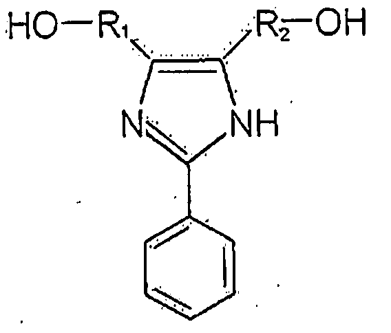
(상기에서 R1 및 R2는 각각 독립적으로 탄소수 1~10의 알킬렌기임)
또 다른 구체예에서 상기 반도체용 접착 조성물은 아크릴계 고분자 수지, 에폭시계 수지 및 이미다졸 화합물을 포함하는 조성물이며, 상기 에폭시계 수지는 당량이 약 250 g/eq 이하이고, 상기 이미다졸 화합물은 융점이 약 200 ℃ 내지 약 270℃이며, 상기 조성물은 150℃에서 1분 후 경화잔존율이 약 90 % 이상이며, 260℃에서 20sec 후 경화잔존율이 약 15 % 이하일 수 있다.
또 다른 구체예에서 상기 반도체용 접착 조성물은 아크릴계 고분자 수지, 에폭시계 수지 및 이미다졸 화합물을 포함하며, pH가 약 4.8 내지 약 8 일 수 있다.
상기 에폭시계 수지는 당량이 약 250 g/eq 이하이며, 150 ℃에서 용융점도가 약 0.01 내지 약 0.2 Pa·s 일 수 있다.
상기 조성물은 접착력이 약 15 내지 약 30 kgf/25mm2 일 수 있다.
상기 조성물은 아크릴계 고분자 수지, 에폭시계 수지, 이미다졸 화합물, 실란 커플링제 및 충진제를 포함할 수 있다.
구체예에서 상기 조성물은 아크릴계 고분자 수지 약 20~60 중량%, 에폭시계 수지 약 10~60 중량%, 이미다졸 화합물 약 0.5~12 중량%, 실란 커플링제 약 0.01~5 중량% 및 충진제 약 15~40 중량% 를 포함할 수 있다.
상기 아크릴계 고분자 수지는 에폭시기를 함유하며, 유리전이온도가 약 -30 ~ 80℃일 수 있다.
상기 조성물은 본딩 후 금속 범프에 대한 솔더의 접촉각이 약 10 내지 약 80 도일 수 있다.
본 발명의 다른 관점은 상기 접착 조성물을 금속 범프와 솔더의 접착제 용도로 사용하는 방법에 관한 것이다.
본 발명의 다른 관점은 상기 접착 조성물로 형성된 반도체용 접착 필름을 제공한다.
또한 본 발명의 또 다른 관점은 상기 접착 필름으로 접착된 반도체 패키지를 제공한다. 상기 반도체 패키지는 칩 탑재 기판; 및 상기 집 탑재 기판의 일면에 적층된 제1 및 제2 반도체 칩을 포함하며, 상기 제1 및 제2 반도체 칩은 상기 접착 필름으로 접착된 것을 특징으로 한다.
본 발명은 Flux기능과 절연 접착층의 속경화를 동시에 가능하게 하면서 조액 안정성 및 실장 이후 잔류하는 산에 의한 불량을 없앨 수 있고, 본딩 시 빠른 경화 반응이 진행될 수 있고, 에폭시와의 반응에 의한 경화제 활성 저하와 이에 따른 미반응 경화체 잔류물의 고온 분해와 같은 불량이 발생하지 않으며, 250℃ 이상의 다이본딩하는 TSV(throung silicon via) 패키징에서도 안정적으로 적용할 수 있고, 범프 Chip간 전기적 접속 신뢰성이 우수며, Cu Bump와 솔더의 산화막을 제거하는 Flux공정이 가능하고, 가열 압착에 따른 Chip Bonding시 Bump와 솔더가 충분히 서로 접속하게 할 수 있는 고유동의 반도체용 접착 조성물, 이를 포함하는 접착 필름과 상기 접착 필름을 이용한 반도체 패키지를 제공하는 발명의 효과를 갖는다.
한 구체예에서 본 발명의 접착 조성물은 아크릴계 고분자 수지, 에폭시계 수지, 이미다졸 화합물, 실란 커플링제 및 충진제를 포함할 수 있다.
구체예에서는 상기 조성물은 아크릴계 고분자 수지 약 20~60 중량%, 에폭시계 수지 약 10~60 중량%, 이미다졸 화합물 약 0.5~12 중량%, 실란 커플링제 약 0.01~5 중량% 및 충진제 약 15~40 중량% 를 포함할 수 있다.
아크릴계 고분자 수지
상기 아크릴계 고분자 수지는 (메타)아크릴레이트 공중합체를 단독으로 사용하거나 (메타)아크릴레이트 공중합체에 다른 고분자 수지와 혼합하여 사용할 수도 있다. 바람직하게는 상기 (메타)아크릴레이트 공중합체는 에폭시기를 함유할 수 있다. 구체예에서는 상기 아크릴계 고분자 수지는 에폭시 당량이 약 500~5000 g/eq 인 것이 사용될 수 있다. 상기 범위에서 경화된 조성물의 신뢰도가 뛰어난 장점이 있다.
상기 아크릴계 고분자 수지는 중량평균분자량이 약 50,000 내지 약 5,000,000g/mol, 바람직하게는 약 100,000 내지 약 1,000,000 g/mol 일 수 있다. 상기 범위에서 필름 형성능과 조성물의 기계적 성질 및 보이드 제거 능력이 뛰어난 장점이 있다.
하나의 구체예에서 상기 아크릴계 고분자 수지는 알킬(메타)아크릴레이트 모노머와 글리시딜 (메타)아크릴레이트 모노머의 공중합체일 수 있다.
상기 알킬(메타)아크릴레이트 모노머는 필름에 점착력을 부여하는 기능을 하는 것으로서, 2-에틸헥실메타크릴레이트, 이소 옥틸 아크릴레이트, 2-에틸헥실아크릴레이트, 에틸아크릴레이트, n-부틸아크릴레이트, iso-부틸아크릴레이트 및 옥타데실메타크릴레이트 등이 사용될 수 있으며, 반드시 이에 제한되는 것은 아니다.
상기 글리시딜 (메타)아크릴레이트 모노머는 글리시딜 메타크릴레이트 또는 글리시딜 아크릴레이트 등이 있으며, 반드시 이에 제한되는 것은 아니다.
다른 구체예에서는 상기 모노머외에 수산기 함유 (메타)아크릴레이트 모노머도 선택적으로 부가되어 공중합될 수 있다. 상기 수산기 함유 (메타)아크릴레이트 모노머로는 2-하이드록시에틸 메타아크릴레이트, 2-하이드록시에틸 아크릴레이트, 3-하이드록시프로필 메타아크릴레이트, 3-하이드록시프로필 아크릴레이트, 하이드록시프로필 (메타)아크릴레이트, 4-하이드록시부틸 아크릴레이트, N-(하이드록시메틸) 아크릴레이트, 3-클로로-2-하이드록시프로필 메타아크릴레이트 등이 있으며, 반드시 이에 제한되는 것은 아니다.
상기 아크릴계 고분자 수지는 유리전이온도가 약 -30 ~ 80℃, 바람직하게는 약 0 ~ 60℃, 보다 바람직하게는 약 5 ~ 35℃일 수 있다. 상기 범위에서 고유동을 확보할 수 있어 보이드 제거 능력이 우수하고, 접착력 및 신뢰성을 얻을 수 있다.
상기 아크릴계 고분자 수지는 25℃ 점도가 약 1,000 내지 약 30,000 cps 일 수 있다. 상기 범위에서 조성물의 치수 균일성과 필름 형성능이 뛰어난 장점이 있다.
상기 아크릴계 고분자 수지는 전체 반도체용 접착 조성물중 약 20~60 중량%(고형분 기준), 바람직하게는 약 22~50 중량%, 더욱 바람직하게는 약 25~45 중량%이다. 상기 범위에서 우수한 신뢰성과 발포성 보이드 제거 효과를 얻을 수 있다.
에폭시계 수지
상기 에폭시계 수지는 경화 및 접착 작용을 하는 것으로서, 당량이 약 250 g/eq 이하인 것이 사용될 수 있다. 상기 범위에서 경화반응에 의한 경화밀도의 증가로 인해 접착 조성물의 접착력 및 발포성 보이드 억제력, 경화후 내흡습성이 증가하여 신뢰도를 높일 수 있다. 바람직하게는 약 100 내지 약 250 g/eq, 더 바람직하게는 약 200 내지 약 245g/eq일 수 있다.
또한 상기 에폭시계 수지는 150℃에서의 용융점도가 약 0.001~0.2 Pa·s 인 것이 사용될 수 있다. 상기 범위에서 착 조성물의 흐름성이 우수하여 Bump간 접속이 원활하게 된다. 바람직하게는 약 0.01 내지 약 0.1 Pa·s 이며, 더욱 바람직하게는 약 0.01~0.09 Pa·s이다.
상기 에폭시 수지의 중량평균분자량은 약 100 내지 약 5000 g/mol 인 것이 사용될 수 있다. 상기 범위에서 흐름성이 뛰어난 장점이 있다.
상기 에폭시계 수지는 전체 조성물(고형분 기준)중 약 10~60 중량%, 바람직하게는 약 20~50 중량%, 더욱 바람직하게는 약 25~45 중량%로 포함될 수 있다. 상기 범위에서 우수한 신뢰성 및 기계적 물성을 얻을 수 있다.
이미다졸 화합물
본 발명의 이미다졸 화합물은 융점이 약 200 ℃ 이상인 것을 특징으로 한다. m.p가 200도 이하인 이미다졸 화합물을 사용할 경우 상대적으로 경화 반응이 빨리 시작되게 되어 접착 필름의 유동 특성이 저하되고 이에 따른 Bump간 접속성이 불량해진다. 바람직하게는 융점이 약 200~270 ℃의 범위이며, 바람직하게는 약 210~265 ℃이다.
상기 이미다졸 화합물은 Flux활성을 나타내면서 에폭시 수지와 경화반응도 동시에 가능하게 하며, 특히 특정 용융점도 범위와 당량을 갖는 에폭시계 수지를 사용하여 TSV用 절연 접착필름 조성물의 용융 특성과 속경화성을 만족시킬 수 있다.
구체예에서 상기 이미다졸 화합물은 하기 화학식 1로 표시될 수 있다:
[화학식 1]
[규칙 제26조에 의한 보정 09.01.2012]
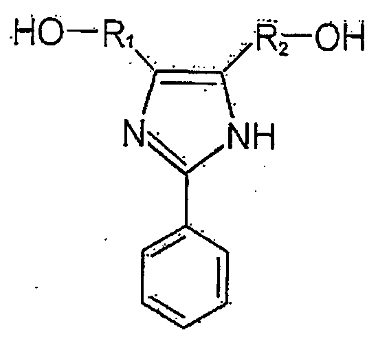
(상기에서 R1 및 R2는 각각 독립적으로 탄소수 1~10의 알킬렌기임)
바람직하게는 상기 R1 및 R2는 각각 독립적으로 탄소수 1~5의 알킬렌기이며, 더욱 바람직하게는 탄소수 1~3의 알킬렌기이다.
상기 이미다졸 화합물은 전체 조성물(고형분 기준)중 약 약 0.5~12 중량%, 바람직하게는 약 5.5~10 중량%로 포함될 수 있다. 상기 범위에서 접착력이 우수하고, 발포성 보이드를 최소화할 수 있으며, 흡습 등의 불량이 발생하지 않고, 접속성 불량이 발생하지 않는다.
실란 커플링제
실란 커플링제는 조성물 배합시 실리카와 같은 무기물질의 표면과 유기물질간의 화학적 결합으로 인한 접착력을 증진시키기 위한 접착증진제의 작용을 한다.
상기 커플링제는 통상적으로 사용되는 실란 커플링제를 사용할 수 있으며, 예를 들어 에폭시가 함유된 2-(3,4 에폭시 사이클로 헥실)-에틸트리메톡시실란, 3-글리시독시트리메톡시실란, 3-글리시독시프로필트리에톡시실란, 아민기가 함유된 N-2(아미노에틸)3-아미토프로필메틸디메톡시실란, N-2(아미노에틸)3-아미노프로필트리메톡시실란, N-2(아미노에틸)3-아미노프로필트리에톡시실란, 3-아미노프로필트리메톡시실란, 3-아미노프로필트리에톡시실란, 3-트리에톡시실리-N-(1,3-디메틸뷰틸리덴)프로필아민, N-페닐-3-아미노프로필트리메톡시실란, 머캅토가 함유된 3-머캅토프로필메틸디메톡시실란, 3-머캅토프로필트리에톡시실란, 이소시아네이트가 함유된 3-이소시아네이트프로필트리에톡시실란 등이 있으며, 이들을 단독 또는 2종 이상을 혼합하여 사용할 수 있다.
상기 커플링제는 전체 접착 조성물(고형분 기준)중 약 0.1 내지 약 5 중량%, 바람직하게는 약 0.5 내지 약 3 중량%, 더욱 바람직하게는 약 0.7 내지 약 2 중량%이다. 상기 범위에서 접착신뢰성이 우수하고 기포발생 문제를 줄일 수 있다.
충진제
상기 충진제는 금속성분인 금분, 은분, 동분, 니켈을 사용할 수 있고, 비금속성분인 알루미나, 수산화알루미늄, 수산화마그네슘, 탄산칼슘, 탄산마그네슘, 규산칼슘, 규산마그네슘, 산화칼슘, 산화마그네슘, 산화알루미늄, 질화알루미늄, 실리카, 질화붕소, 이산화티타늄, 유리, 산화철, 세라믹 등을 사용할 수 있다. 이중 바람직하게는 실리카이다.
상기 충진제의 형상과 크기는 특별히 제한되지 않으나, 통상적으로 충진제 중에서는 구형 실리카와 무정형 실리카가 주로 사용되고, 그 크기는 약 5㎚ 내지 약 20㎛인 것이 바람직하다.
상기 충진제는 전체 접착 조성물(고형분 기준)중 약 15~40 중량%로 포함될 수 있다. 바람직하게는 약 20~35 중량%이다. 상기 범위에서 우수한 유동성과 필름형성성 및 접착성을 가질 수 있다.
상기 접착 조성물은 유기용매를 추가로 포함할 수 있다. 상기 유기용매는 반도체용 접착 조성물의 점도를 낮게 하여 필름의 제조가 용이하도록 한다. 구체적으로 톨루엔, 자일렌, 프로필렌 글리콜 모노메틸 에테르 아세테이트, 벤젠, 아세톤, 메틸에틸케톤, 테트라히드로 퓨란, 디메틸포름알데히드, 시클로헥사논 등을 사용할 수 있으며, 반드시 이에 제한되지 않는다.
상기 조성물은 150 ℃에서 용융점도가 약 2 ×10⁴ 내지 약 15 ×104 poise 일 수 있다. 바람직하게는 약 4×10⁴ 내지 약 10 ×104 poise일 수 있다. 상기 범위일 경우, 금속 범프와 솔더간의 원활한 접촉을 가지므로 전기 접속이 잘 이루어 질 수 있다.
상기 조성물은 본딩 후 금속 범프에 대한 Solder의 접촉각이 약 10 내지 약 80 도일 수 있다. 상기 접촉각일 경우, solder의 산화막이 제거 되면 표면에너지가 높아져서 우수한 wetting을 가지고 금속 범프와 solder의 전기 접속이 잘 이루어진다. 구체예에서는 접촉각이 25 내지 75 도, 예를 들면 35 내지 60도 일 수 있다.
또한 상기 조성물은 접착력이 약 15 내지 약 30 kgf/25mm2, 바람직하게는 15 내지 25 kgf/25mm2일 수 있다.
상기 조성물은 150℃에서 1분 후 경화잔존율이 약 90 % 이상, 바람직하게는 95 %이상이며, 260℃에서 20sec 후 경화잔존율이 약 15 % 이하, 바람직하게는 10 % 이하일 수 있다.
본 발명의 접착 조성물은 pH가 약 4.8 내지 약 8 , 바람직하게는 약 6 내지 약 8, 더욱 바람직하게는 약 6.2 내지 약 7.6 일 수 있다. 상기 범위일 경우, Flux기능과 절연 접착층의 속경화를 동시에 가능하게 하면서 조액 안정성 및 실장 이후 잔류하는 산에 의한 불량이 없게 된다.
본 발명의 다른 관점은 상기 접착 조성물로 형성된 반도체용 접착 필름에 관한 것이다. 상기 접착 필름은 범프 Chip간 전기적 접속 신뢰성을 만족하는 접착층을 형성하며, Cu Bump와 솔더의 산화막을 제거하는 Flux공정이 가능하다. 또한 가열 압착에 따른 Chip Bonding시 Bump와 솔더가 충분히 서로 접속하게 할 수 있다. 또한 접착력이 우수할 뿐만 아니라, 발포성 보이드가 발생하지 않고 Bump와 솔더간 imc 층을 충분한 면적으로 형성할 수 있다.
한 구체예에서는 상기 접착 조성물은 금속 범프와 솔더의 접착제 용도로 사용될 수 있다. 다른 구체에에서는 상기 접착 조성물은 칩(chips)간 접착제 용도로 사용될 수 있다.
본 발명은 하기의 실시예에 의하여 보다 더 잘 이해 될 수 있으며, 하기의 실시예는 본 발명의 예시목적을 위한 것이며 첨부된 특허청구범위에 의하여 한정되는 보호범위를 제한하고자 하는 것은 아니다.
하기 실시예 및 비교예에서 사용된 각 성분의 사양은 다음과 같다:
(A) 아크릴계 고분자 수지(SG-P3, 나가세 켐텍스)
(B) 에폭시계 수지
(b1)CER-3000L, 일본화약, 에폭시 당량 240 g/eq, 0.05 Pa·s(150 ℃, ICI)
(b2)NC-7300L, 일본화약, 에폭시 당량 214 g/eq, 0.05 Pa·s(150 ℃, ICI)
(b3)NC-3000H, 일본화약, 에폭시 당량 290 g/eq, 0.30 Pa·s(150 ℃, ICI)
(C) 이미다졸 화합물
(c1)2P4MZ, 사국화학(m.p. 179 ℃)
(c2)2P4MHZ, 사국화학(m.p. 193 ℃)
(c3)2PHZ, 사국화학(m.p. 230 ℃)
(D) 실란커플링제: 에폭시 실란 커플링제 (KBM-303, 제조원: 신에쯔주식회사)
(E) 충진제: 구형 실리카 (SC-2500SQ, 제조원: 아드마텍스(Admatechs)
(F) 용매: 메틸에틸케톤 (제조원: 삼전화학)
실시예 1~6 및 비교예 1~3
고속 교반봉을 포함하는 1L 원통형 플라스크에 하기 표 1 및 2에 기재된 성분을 첨가하고 10분간 2000 rpm에서 저속으로, 그리고 30분간 5000rpm에서 고속으로 분산하여 접착 필름용 조성물을 제조하였다. 이후, 각 조성물을 50㎛ 캡슐 필터를 이용하여 여과한 뒤 어플리케이터로 PET 필름에 20㎛ 두께로 코팅하여 접착 필름을 제조하였으며, 90℃에서 10분 건조한 뒤 110 ℃에서 5분간 건조한 후 실온에서 1일간 보관하였다.
상기 실시예1 ~ 6 및 비교예1 ~ 3에서 제조된 접착 필름을 이용하여 하기와 같은 방법으로 실험하였다.
(1) 용융점도 at 150℃ (× 104[P]) : 필름의 점도를 측정하기 위하여 각각의 필름을 여러 겹으로 60℃에서 합지하고 지름이 8mm로 원형 컷팅하였다. 이때 두께는 400 ~ 450um정도이다. 점도측정범위는 30℃에서 300℃까지 측정하였고 승온조건은 5℃/분이다. 표에는 칩간 접착이 행해지는 온도인 150℃에서의 흐름성을 가늠하는 150℃에서의 에타(Eta) 값을 나타내었다. 경화 반응의 진행에 의해 150℃에서의 용융점도가 높아진다면 Bump간 최종 접속을 하게 되는 260℃에서의 짧은 시간의 어태치 공정에서 Bump간 접속이 되지 않을 수 있다.
(2)접착력 [kgf/25mm2] : 이산화 막으로 코팅되어있는 두께 725um 제1웨이퍼를 5mm x 5mm 크기로 자른 뒤 상기에서 제조된 접착 필름과 함께 60도 조건에서 라미네이션(Lamination)하고 접착부분만 남기고 절단하였다. 상기 제1웨이퍼와 동일한 두께 725um이고, 10mm x 10mm 크기의 제2 웨이퍼 위에 상기 접착필름이 라미네이션된 제1웨이퍼 조각을 10초 동안 1.0 kgf의 힘으로 150℃ 1분, 260℃ 20초의 순서로 압착하고 260℃에서의 전단 파괴 강도를 측정했다.
(3) 발포성 void : 이산화 막으로 코팅되어있는 두께 80um 제1웨이퍼를 10mm x 10mm 크기로 자른 뒤 상기에서 제조된 접착 필름과 함께 60도 조건에서 라미네이션(Lamination)하고 접착부분만 남기고 절단하였다. 두께 725um인 10mm x 10mm 크기의 제2웨이퍼 위에 상기 접착필름이 라미네이션된 제1웨이퍼 조각을 1.0 kgf의 힘으로 150℃ 1분, 260℃ 20초 각각 순서대로 압착하고 SAT(Scanning Acoustic Tomograph)로 조사하여 발포성 void의 양호수준을 평가하였다. 발포 없이 면상 양호하면 ○, 부분적으로 미세 발포가 발생하면 △, 발포 현상이 심하면 ×로 표시하였다.
(4) 150℃ 1min 후 경화잔존율 (%) : 상기 실시예 1 내지 6 및 비교예 1 내지 3의 접착 조성물을 이용하여 제조한 접착필름을 각각 10㎜×30㎜로 자른 뒤 커버 필름(cover film)을 벗기고 슬라이드글라스에 60℃ 조건에서 라미네이션(Lamination)한 뒤, PET 필름을 벗기고 150℃의 핫 플레이트(hot plate)에서 1분간 경화시켰다. 이후, 상기 슬라이드 글라스로부터 제거하여 경화발열량을 측정하고 하기 식 1에 따라 경화잔존율을 계산하였다. 경화발열량은 시차주사열량계(DSC)를 이용하여 승온속도는 10℃/분, 50~300℃까지 스캔하여 측정하였다. 150℃ 1분의 경화 후 경화잔존율이 높을 수록 접착 조성물의 흐름성이 확보되어 추후 이어지는 260℃ 에서의 최종 Bump접속에 유리하다.
[식 1]

초기발열량(Hi): 필름 제작후 발열량
경화후 발열량(Hc): 150℃ 1분의 경화 후 발열량
(5) 260℃ 20sec 후 경화잔존율 (%) : 상기 실시예 1 내지 6 및 비교예 1 내지 3의 접착필름 조성물을 이용하여 제조한 접착필름을 각각 10㎜×30㎜로 자른 뒤 커버 필름(cover film)을 벗기고 슬라이드글라스에 60℃ 조건에서 라미네이션(Lamination)한 뒤, PET 필름을 벗기고 260℃의 핫 플레이트(hot plate)에서 20초간 경화시켰다. 이후, 상기 슬라이드 글라스로부터 제거하여 경화발열량을 측정하고 상기 식 1에 따라 경화잔존율을 계산하였다. 이때 경화후 발열량(Hc)은 260℃ 20초의 경화 후 발열량이다. 경화발열량은 시차주사열량계(DSC)를 이용하여 승온속도는 10℃/분, 50~300℃까지 스캔하여 측정하였다. 260℃ 20초의 경화 후 경화잔존율이 낮을 수록 접착 조성물의 경화밀도가 높아지게 되어 접착 조성물의 신뢰성이 우수해진다.
(6) 경화 후 흡습율(%) : 상기 실시예 1 내지 6 및 비교예 1 내지 3의 접착필름 조성물을 이용하여 제조한 접착필름을 각각 5㎜ × 5㎜ 의 크기로 잘라 500um두께로 라미네이션 한 뒤, 85℃/85% 항온항습기에 168시간 방치하였다. 방치 전 후의 무게를 측정하여 하기 식 2에 의해 경화 후 흡습율을 구하였다.
[식 2]

Wa: 초기 무게
Wb: 방치 후 무게
(7) 솔더/Cu Bump 접속성 : 솔더 Bump와 Cu Bump의 접속성 평가를 위해 제작된 칩을 사용하여 접착제 조성에 따른 Bump to Bump의 접속성 양호수준을 평가하였다. 접속이 양호하면 ○, 부분적으로 접속이 안되면 △, 모든 부분에서 접속이 안되면 ×로 표시하였다.
(8) 솔더/Cu間 IMC Layer유무 : 솔더 Bump와 Cu Bump접속 시 Flux활성에 따른 산화막 제거가 발현된다면 솔더/Cu間 IMC(Intermetallic Compound) Layer가 생성된다. (ref. Journal of Alloys and Compounds 381 (2004) 151 157) 산화막 제거능에 대한 평가를 위해 Cu foil에 접착 필름과 솔더 Ball (Sn96.8Ag3.0Cu0.2, 760um)을 올려 놓고 260℃로 압착하여 몰딩한 후 측면을 polishing하여 Cu foil과 솔더 ball 사이의 IMC layer를 SEM을 이용하여 관찰하였다. IMC layer가 있으면 ○, 없으면 ×로 표시하였다.
(9) 접촉각(도): Cu foil에 접착 필름과 솔더 Ball (Sn96.8Ag3.0Cu0.2, 두께 760um)을 순차적으로 올려 놓고 260℃로 압착하여 몰딩한 후 측면을 polishing하여 Cu foil과 솔더 ball 사이의 접촉 부분을 SEM을 이용하여 관찰하였다. 이때 Flux활성에 따른 산화막 제거가 발현된다면 Cu foil면에 솔더 ball이 wetting하게 되고 접촉 부분에서 접촉각 측정이 가능하게 된다.
(10) pH : 경화되지 않은 접착 필름을 1.75g 채취하여 Nalgen bottle에 DI water 80g과 함께 담아 밀봉한 후 Pressure Cooker Test Machine에서 121℃, 100% 습도 조건으로 48시간 aging한다. 용출된 DI water에 대해 pH meter로 pH를 측정한다.
표 1
| 실시예 1 | 실시예 2 | 실시예 3 | 실시예 4 | 실시예 5 | 실시예 6 | |
| (A) | 25 | 25 | 25 | 25 | 25 | 25 |
| (b1) | 37 | 44 | - | 6.5 | 37 | - |
| (b2) | 7 | - | 40.5 | 34 | - | 37 |
| (b3) | - | - | - | - | - | - |
| (c1) | - | - | - | - | - | - |
| (c2) | - | - | - | - | - | - |
| (c3) | 5 | 5 | 8.5 | 8.5 | 12 | 12 |
| (D) | 1 | 1 | 1 | 1 | 1 | 1 |
| (E) | 25 | 25 | 25 | 25 | 25 | 25 |
| 용융점도 | 5.6 | 8.3 | 8.5 | 5.4 | 6.3 | 7.5 |
| 접착력 | 15 | 15 | 18 | 17 | 22 | 24 |
| 발포성 void | ○ | ○ | ○ | ○ | ○ | ○ |
| 150℃ 1min 후 경화잔존율 | 100 | 100 | 100 | 100 | 100 | 100 |
| 260℃ 20sec 후 경화잔존율 | 14 | 14 | 11 | 13 | 9 | 7 |
| 경화 후 흡습 | 0.5 | 0.5 | 0.4 | 0.5 | 0.5 | 0.8 |
| 솔더/Cu Bump 접속성 | ○ | ○ | ○ | ○ | ○ | ○ |
| 솔더/Cu間 IMC Layer유무 | ○ | ○ | ○ | ○ | ○ | ○ |
| 접촉각 | 38 | 42 | 35 | 36 | 35 | 36 |
| pH | 7.1 | 7.1 | 7.37 | 7.37 | 7.55 | 7.55 |
표 2
| 비교예 | ||||
| 1 | 2 | 3 | 4 | |
| (A) | 25 | 25 | 25 | 25 |
| (b1) | 44 | 22 | - | 49.7 |
| (b2) | - | 22 | - | |
| (b3) | - | - | 44 | |
| (c1) | 5 | - | - | 0.3 |
| (c2) | - | 5 | - | |
| (c3) | - | - | 5 | |
| (D) | 1 | 1 | 1 | 1 |
| (E) | 25 | 25 | 25 | 25 |
| 용융점도 | 15.3 | 13.0 | 16.5 | 14.5 |
| 접착력 | 12 | 13 | 4 | 10 |
| 발포성 void | ○ | ○ | △ | ○ |
| 150℃ 1min 후 경화잔존율 | 85 | 89 | 100 | 92 |
| 260℃ 20sec 후 경화잔존율 | 16 | 15 | 37 | 40 |
| 경화 후 흡습 | 0.7 | 0.7 | 1.8 | 1.7 |
| 솔더/Cu Bump 접속성 | × | × | × | ○ |
| 솔더/Cu間 IMC Layer유무 | ○ | ○ | ○ | × |
| 접촉각 | 30 | 34 | 30 | × |
| pH | 7.1 | 7.1 | 7.1 | 4.62 |
상기 표 1~2에 나타난 바와 같이 실시예 1-6은 모든 측정 항목에서 양호한 것을 알 수 있다. 반면, 비교예 3에서는 발포성 보이드가 발생하였으며, 260 도에서 경화후 경화잔존율이 높게 나타났다. 비교예 1~3 은 솔더/Cu Bump 접속성이 모두 실패하였다.
본 발명은 상기 실시예들에 한정되는 것이 아니라 서로 다른 다양한 형태로 제조될 수 있으며, 본 발명이 속하는 기술분야에서 통상의 지식을 가진 자는 본 발명의 기술적 사상이나 필수적인 특징을 변경하지 않고서 다른 구체적인 형태로 실시될 수 있다는 것을 이해할 수 있을 것이다. 그러므로 이상에서 기술한 실시예들은 모든 면에서 예시적인 것이며 한정적이 아닌 것으로 이해해야 한다.
Claims (12)
- 아크릴계 고분자 수지, 에폭시계 수지 및 이미다졸 화합물을 포함하는 조성물이며,상기 이미다졸 화합물은 융점이 약 200 ℃ 내지 약 270℃이며,상기 조성물은 150 ℃에서 용융점도가 약 2 ×10⁴ 내지 약 15 ×104 poise 인 것을 특징으로 하는 반도체용 접착 조성물.
- [규칙 제26조에 의한 보정 09.01.2012]
아크릴계 고분자 수지, 에폭시계 수지 및 이미다졸 화합물을 포함하는 조성물이며,상기 이미다졸 화합물은 하기 화학식 1로 표시되는 것을 특징으로 하는 반도체용 접착 조성물:[화학식 1]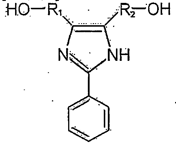 (상기에서 R1 및 R2는 각각 독립적으로 탄소수 1~10의 알킬렌기임).
 - 아크릴계 고분자 수지, 에폭시계 수지 및 이미다졸 화합물을 포함하는 조성물이며,상기 에폭시계 수지는 당량이 약 250 g/eq 이하이고,상기 이미다졸 화합물은 융점이 약 200 ℃ 내지 약 270℃이며,상기 조성물은 150℃에서 1분 후 경화잔존율이 약 90 % 이상이며, 260℃에서 20sec 후 경화잔존율이 약 15 % 이하인 것을 특징으로 하는 반도체용 접착 조성물.
- 아크릴계 고분자 수지, 에폭시계 수지 및 이미다졸 화합물을 포함하는 조성물이며, pH가 약 4.8 내지 약 8인 반도체용 접착 조성물.
- 제1항 내지 제4항중 어느 한 항에 있어서, 상기 에폭시계 수지는 당량이 약 200 g/eq 초과 약 250 g/eq 이하이며, 150 ℃에서 용융점도가 약 0.01 내지 약 0.2 Pa·s 인 반도체용 접착 조성물.
- 제1항 내지 제4항중 어느 한 항에 있어서, 상기 조성물은 접착력이 약 15 내지 약 30 kgf/25mm2 인 반도체용 접착 조성물.
- 제1항 내지 제4항중 어느 한 항에 있어서, 상기 조성물은 아크릴계 고분자 수지, 에폭시계 수지, 이미다졸 화합물, 실란 커플링제 및 충진제를 포함하는 반도체용 접착 조성물.
- 제7항에 있어서, 상기 조성물은 아크릴계 고분자 수지 약 20~60 중량%, 에폭시계 수지 약 10~60 중량%, 이미다졸 화합물 약 0.5~12 중량%, 실란 커플링제 약 0.01~5 중량% 및 충진제 약 15~40 중량% 를 포함하는 반도체용 접착 조성물.
- 제1항 내지 제4항중 어느 한 항에 있어서, 상기 아크릴계 고분자 수지는 에폭시기를 함유하며, 유리전이온도가 약 -30 ~ 80℃인 것을 특징으로 하는 반도체용 접착 조성물.
- 제1항 내지 제4항중 어느 한 항에 있어서, 상기 조성물은 본딩 후 금속 범프에 대한 솔더의 접촉각이 약 10 내지 약 80 도인 반도체용 접착 조성물.
- 제1항 내지 제4항중 어느 한 항의 접착 조성물을 금속 범프와 솔더의 접착제 용도로 사용하는 방법.
- 제1항 내지 제4항중 어느 한 항의 접착 조성물로 형성된 반도체용 접착 필름.
Applications Claiming Priority (2)
| Application Number | Priority Date | Filing Date | Title |
|---|---|---|---|
| KR10-2010-0130088 | 2010-12-17 | ||
| KR20100130088 | 2010-12-17 |
Publications (2)
| Publication Number | Publication Date |
|---|---|
| WO2012081842A2 true WO2012081842A2 (ko) | 2012-06-21 |
| WO2012081842A3 WO2012081842A3 (ko) | 2012-09-07 |
Family
ID=46245182
Family Applications (1)
| Application Number | Title | Priority Date | Filing Date |
|---|---|---|---|
| PCT/KR2011/008775 Ceased WO2012081842A2 (ko) | 2010-12-17 | 2011-11-16 | 반도체용 접착 조성물, 이를 포함하는 접착 필름 및 그 용도 |
Country Status (2)
| Country | Link |
|---|---|
| KR (1) | KR20120068695A (ko) |
| WO (1) | WO2012081842A2 (ko) |
Cited By (2)
| Publication number | Priority date | Publication date | Assignee | Title |
|---|---|---|---|---|
| US20240269967A1 (en) * | 2020-08-18 | 2024-08-15 | Lignom Holding S.À R.L. | Adhesive formulation for producing pressed material molded bodies |
| KR102959325B1 (ko) | 2023-09-01 | 2026-04-30 | 창 춘 플라스틱스 컴퍼니, 리미티드 | 감광성 수지 라미네이트 및 그 용도 |
Family Cites Families (4)
| Publication number | Priority date | Publication date | Assignee | Title |
|---|---|---|---|---|
| JPWO2007125650A1 (ja) * | 2006-04-27 | 2009-09-10 | 住友ベークライト株式会社 | 接着テープ、半導体パッケージおよび電子機器 |
| KR101082448B1 (ko) * | 2007-04-30 | 2011-11-11 | 주식회사 엘지화학 | 접착 수지 조성물 및 이를 이용한 다이싱 다이 본딩 필름 |
| KR20090103434A (ko) * | 2008-03-28 | 2009-10-01 | 제일모직주식회사 | 반도체 조립용 접착 필름용 조성물, 이에 의한 접착 필름및 이를 포함하는 다이싱 다이 본드 필름 |
| KR101035873B1 (ko) * | 2008-12-24 | 2011-05-19 | 제일모직주식회사 | 고온 속경화형 접착필름 조성물 및 이를 이용한 접착필름 |
-
2011
- 2011-11-16 WO PCT/KR2011/008775 patent/WO2012081842A2/ko not_active Ceased
- 2011-11-17 KR KR1020110120484A patent/KR20120068695A/ko not_active Ceased
Cited By (2)
| Publication number | Priority date | Publication date | Assignee | Title |
|---|---|---|---|---|
| US20240269967A1 (en) * | 2020-08-18 | 2024-08-15 | Lignom Holding S.À R.L. | Adhesive formulation for producing pressed material molded bodies |
| KR102959325B1 (ko) | 2023-09-01 | 2026-04-30 | 창 춘 플라스틱스 컴퍼니, 리미티드 | 감광성 수지 라미네이트 및 그 용도 |
Also Published As
| Publication number | Publication date |
|---|---|
| WO2012081842A3 (ko) | 2012-09-07 |
| KR20120068695A (ko) | 2012-06-27 |
Similar Documents
| Publication | Publication Date | Title |
|---|---|---|
| CN101899195B (zh) | 坝料组合物及多层半导体装置的制造方法 | |
| US6621170B2 (en) | Semiconductor device, substrate for mounting semiconductor chip, processes for their production, adhesive, and double-sided adhesive film | |
| JP4537555B2 (ja) | 半導体パッケージの製造方法及び半導体パッケージ | |
| KR101690626B1 (ko) | 반도체 장치 및 그 제조 방법 | |
| WO1998028788A1 (fr) | Production dun dispositif a semi-conducteur | |
| WO2004060996A1 (ja) | 硬化性樹脂組成物、接着性エポキシ樹脂ペースト、接着性エポキシ樹脂シート、導電接続ペースト、導電接続シート及び電子部品接合体 | |
| CN110556344A (zh) | 半导体用粘接剂、半导体装置的制造方法以及半导体装置 | |
| WO2005117093A1 (ja) | 半導体封止用樹脂シートおよびこれを用いた半導体装置の製造方法 | |
| WO2012043923A1 (ko) | 반도체 패키지 제작용 접착제 조성물 및 접착시트 | |
| JP2004315688A (ja) | 半導体用接着フィルム、半導体装置、及び半導体装置の製造方法。 | |
| JPH11265960A (ja) | 金属製補強材付き半導体装置 | |
| JP3999840B2 (ja) | 封止用樹脂シート | |
| JP4161544B2 (ja) | 半導体素子搭載用接着フィルム | |
| KR102012789B1 (ko) | 반도체 장치 | |
| WO2012081771A1 (ko) | 반도체용 접착 조성물, 이를 포함하는 접착 필름 및 이를 이용한 반도체 패키지 | |
| TWI834852B (zh) | 半導體用接著劑、半導體裝置的製造方法及半導體裝置 | |
| JP3617504B2 (ja) | 半導体素子搭載用接着フィルム | |
| KR20050076660A (ko) | 반도체 밀봉용 수지 조성물 | |
| TWI906069B (zh) | 半導體用接著劑、半導體裝置的製造方法及半導體裝置 | |
| TW202028391A (zh) | 半導體用膜狀接著劑、半導體裝置及其製造方法 | |
| KR101035873B1 (ko) | 고온 속경화형 접착필름 조성물 및 이를 이용한 접착필름 | |
| TWI895502B (zh) | 半導體用接著劑、以及半導體裝置及其製造方法 | |
| JPH1117075A (ja) | 半導体装置 | |
| WO2013094924A1 (ko) | 반도체용 접착필름 및 이를 이용한 반도체 패키지 | |
| KR20120068695A (ko) | 반도체용 접착 조성물, 이를 포함하는 접착 필름 및 그 용도 |
Legal Events
| Date | Code | Title | Description |
|---|---|---|---|
| 121 | Ep: the epo has been informed by wipo that ep was designated in this application |
Ref document number: 11849190 Country of ref document: EP Kind code of ref document: A2 |
|
| NENP | Non-entry into the national phase |
Ref country code: DE |
|
| 122 | Ep: pct application non-entry in european phase |
Ref document number: 11849190 Country of ref document: EP Kind code of ref document: A2 |