WO2012081375A1 - 光導波路の製造方法 - Google Patents
光導波路の製造方法 Download PDFInfo
- Publication number
- WO2012081375A1 WO2012081375A1 PCT/JP2011/077159 JP2011077159W WO2012081375A1 WO 2012081375 A1 WO2012081375 A1 WO 2012081375A1 JP 2011077159 W JP2011077159 W JP 2011077159W WO 2012081375 A1 WO2012081375 A1 WO 2012081375A1
- Authority
- WO
- WIPO (PCT)
- Prior art keywords
- film
- core
- clad
- optical waveguide
- layer
- Prior art date
- Legal status (The legal status is an assumption and is not a legal conclusion. Google has not performed a legal analysis and makes no representation as to the accuracy of the status listed.)
- Ceased
Links
Images




Classifications
-
- G—PHYSICS
- G02—OPTICS
- G02B—OPTICAL ELEMENTS, SYSTEMS OR APPARATUS
- G02B6/00—Light guides; Structural details of arrangements comprising light guides and other optical elements, e.g. couplings
- G02B6/10—Light guides; Structural details of arrangements comprising light guides and other optical elements, e.g. couplings of the optical waveguide type
- G02B6/12—Light guides; Structural details of arrangements comprising light guides and other optical elements, e.g. couplings of the optical waveguide type of the integrated circuit kind
- G02B6/13—Integrated optical circuits characterised by the manufacturing method
- G02B6/138—Integrated optical circuits characterised by the manufacturing method by using polymerisation
Definitions
- the present invention relates to an optical waveguide manufacturing method.
- This application claims priority based on Japanese Patent Application No. 2010-278178 for which it applied to Japan on December 14, 2010, and uses the content here.
- a method for connecting a film-shaped optical waveguide and an optical device for example, there is a method in which the optical waveguide is incorporated in a PMT connector and connected to the optical device by fitting the connector. At this time, it is necessary not only to perform external processing so as to conform to the connector standard, but also to adapt the core pitch to the connector standard so that there is no optical axis misalignment with the connector at the connection destination.
- the core pitch can be controlled by mask design and drawing accuracy, but if it is a film that shrinks by thermosetting, a design based on the dimensional change rate is required. Also, if there are structures having different thermal shrinkage rates in the optical waveguide, the layers that are in close contact with each other will expand and contract, making it extremely difficult to control. Therefore, instead of accumulating the thermal stress inside the structure, for example, a spacer having a sufficiently small thermal expansion coefficient is engaged between structures having different thermal expansion coefficients without sticking them, and the thermal stress is slid between the structure and the spacer. If the configuration is changed to, the dimensional change may be suppressed. (See Patent Document 1).
- An object of the present invention is to provide a method of manufacturing an optical waveguide that suppresses a dimensional change that occurs during manufacturing.
- a method of manufacturing an optical waveguide comprising: a core layer including a core portion and a cladding portion having a refractive index lower than that of the core portion; and a first cladding layer and a second cladding layer disposed with the core layer interposed therebetween.
- the light according to (1) further including a step of cooling the first cladding layer, the core layer, and the substrate to near room temperature between the first cladding layer stacking step and the substrate removing step.
- a method for manufacturing a waveguide (3) The method for producing an optical waveguide according to any one of (1) and (2), wherein a release treatment is performed on a surface of the base material on the side on which the core layer is formed.
- the layers of the optical waveguide when the layers of the optical waveguide are laminated, the layers are laminated in a state of being fixed on the support base material. For this reason, the free expansion and contraction of each layer is restricted, and the dimensional change that occurs in the manufacturing process of the optical waveguide can be suppressed.
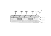
- FIG. 1 is a cross-sectional view of an optical waveguide according to the present invention.
- the optical waveguide 1 sandwiches the core layer 12 having a core layer 121 (hereinafter also referred to as a core film) 12 having a core portion 121 and a cladding portion 122 having a refractive index lower than that of the core portion 121.
- a second cladding layer hereinafter also referred to as a second cladding film 13 (hereinafter referred to as a first cladding layer and a first cladding layer).
- the two cladding layers may be collectively referred to as a cladding layer or a cladding film).
- the core part 121 is a part that forms the optical path of the transmission light, and the cladding part 122 does not form an optical path of the transmission light although it is formed in the core layer 12 and performs the same function as the cladding layers 11 and 13. Part.
- the thickness of the core layer 12 is appropriately set according to the thickness of the optical waveguide 1 to be formed, and is not particularly limited, but is preferably 1 ⁇ m or more and 200 ⁇ m or less, more preferably 5 ⁇ m or more and 100 ⁇ m or less, More preferably, it is 10 ⁇ m or more and 60 ⁇ m or less.
- a material whose refractive index changes by irradiation with light (for example, ultraviolet rays) or further heating is used.
- a resin composition containing a cyclic olefin resin such as a benzocyclobutene polymer or a norbornene polymer as a main material, and including a norbornene polymer (as a main material).
- a resin composition containing a cyclic olefin resin such as a benzocyclobutene polymer or a norbornene polymer as a main material, and including a norbornene polymer (as a main material).
- the core layer 12 made of such a material is excellent in resistance to deformation such as bending, and even when it is repeatedly curved and deformed, the core layer 121 and the clad portion 122 are separated from each other, or the clad layer adjacent to the core layer 12 is used. 11 and 13 hardly occur, and microcracks are prevented from occurring in the core part 121 and the clad part 122. As a result, the optical transmission performance of the optical waveguide 1 is maintained, and the optical waveguide 1 having excellent durability can be obtained.
- Examples of the constituent material of the core layer 12 include an antioxidant, a refractive index adjuster, a plasticizer, a thickener, a reinforcing agent, a sensitizer, a leveling agent, an antifoaming agent, an adhesion aid, and a flame retardant.
- the additive may be contained.
- Addition of an antioxidant has the effect of improving high temperature stability, improving weather resistance, and suppressing light deterioration. Examples of such an antioxidant include phenols such as monophenols, bisphenols, and triphenols, and aromatic amines. Further, the resistance to bending can be further increased by adding a plasticizer, a thickener, and a reinforcing agent.
- the content of additives typified by the antioxidant is preferably about 0.5 to 40% by weight, preferably 3 to 30% by weight, with respect to the entire constituent material of the core layer 12. The degree is more preferable. If this amount is too small, the function of the additive cannot be sufficiently exhibited. If the amount is too large, the transmittance of light (transmitted light) transmitted through the core portion 121 depends on the type and characteristics of the additive. Decrease, patterning failure, refractive index instability and the like.
- the pattern shape of the core portion 121 to be formed is not particularly limited, and is linear, a shape having a curved portion, an irregular shape, a shape having a branching portion of a light path, a merging portion or a crossing portion, a condensing portion (a width or the like is reduced) Or a light diffusing part (a part where the width or the like is increased), or a combination of two or more of these.
- the core portion 121 having any shape can be easily formed by setting the light irradiation pattern.
- the thicknesses of the clad layers 11 and 13 are appropriately set according to the thickness of the optical waveguide 1 to be formed, and are not particularly limited, but are preferably 0.1 ⁇ m or more and 100 ⁇ m or less, and preferably 1 ⁇ m or more and 50 ⁇ m or less. Is more preferably 5 ⁇ m or more and 30 ⁇ m or less.
- a material having a lower refractive index than the core portion 121 of the core layer 12 is used.
- examples include acrylic resins, methacrylic resins, polycarbonates, polystyrenes, epoxy resins, polyamides, polyimides, polybenzoxazoles, cyclic olefin resins such as benzocyclobutene resins and norbornene resins, and one of these.
- Species or a combination of two or more can be used.
- epoxy resins polyimides, polybenzoxazoles, cyclic olefin resins such as benzocyclobutene resins and norbornene resins, and those containing them (mainly) in terms of particularly excellent heat resistance It is preferable to use, and particularly, those mainly composed of norbornene-based resins (norbornene-based polymers) are preferable.
- the norbornene-based polymer is excellent in heat resistance, in an optical waveguide using this as a constituent material of the cladding layers 11 and 13, when the conductor layer is formed in the optical waveguide, the conductor layer is processed to form a wiring. At this time, even when the optical element is mounted, the clad layers 11 and 13 can be prevented from being softened and deformed even if they are heated. Moreover, since it has high hydrophobicity, it is possible to obtain the clad layers 11 and 13 that are less likely to undergo dimensional changes due to water absorption. Norbornene-based polymers or norbornene-based monomers that are raw materials thereof are also preferable because they are relatively inexpensive and easily available.
- the cladding layers 11 and 13 are excellent in resistance to deformation such as bending (bending resistance), even when repeatedly bent and deformed. 13 and the core layer 12 are hardly delaminated, and the occurrence of microcracks in the cladding 122 is also prevented. For this reason, the optical transmission performance of the optical waveguide 1 is maintained, and the optical waveguide 1 having excellent durability is finally obtained.
- each clad layer 11 and 13 are arranged with the core layer 12 interposed therebetween, but each clad layer may be made of the same kind of constituent material or different constituent materials.
- the optical waveguide 1 shown in FIG. 1 has two core parts 121, but the number of core parts 121 formed in one optical waveguide 1 is not particularly limited. Further, in FIG. 1, the core layer 12 is only one layer, but the number of the core layers 12 is not particularly limited, and a plurality of core layers 12 may be laminated.
- optical waveguide manufacturing method (First embodiment) Next, a first embodiment of the optical waveguide manufacturing method of the present invention will be described.
- 2 to 8 are views showing each step of the method of manufacturing an optical waveguide according to the present invention.
- the optical waveguide manufacturing method is as follows: [1] core film preparation step, [2] clad film preparation step, [3] first clad layer lamination step, [4] substrate removal step, [5] second clad layer The description will be divided into lamination steps.
- the core film 12 having the core part 121 having a high refractive index is produced.
- the core film 12 is produced by irradiating light with respect to the film 2 for core formation formed on the core film support base material 41.
- any material can be used as the constituent material of the core-forming film 2 as long as it is a material that is substantially transparent to the propagating light.
- the core forming film 2 is suitably used in data communication using light in a wavelength region of about 600 to 1550 nm, for example. Accordingly, those having sufficient transparency in this wavelength region are preferably used.
- having transparency in the wavelength region of about 600 to 1550 nm is preferably, for example, that the light transmittance in the wavelength region is 90% or more, particularly 99% or more.
- the light transmittance is measured according to JIS K7105. Specifically, a film is formed and cut to a size according to JIS K7105. After setting in a spectrometer and transmitting a white light source through the film, the amount of transmitted light is measured.
- a core film forming material (hereinafter also referred to as a core varnish) 21 is supported by a core film. After being applied to the base material 41, it is formed by a method of curing (solidifying).
- the core film forming material 21 is applied onto the core film supporting substrate 41 by the nozzle 5 capable of controlling discharge, and a liquid film is formed on the core film supporting substrate 41.
- the core film support base 41 rotates in the direction A in FIG. 2, and the nozzle 5 moves in the B direction from the center of the core film support base 41.
- the discharge amount of the core film forming material 21 from the nozzle 5 can be controlled, and is normally set so that the discharge amount increases from the center portion to the end portion of the core film support base 41. ing. Thereby, it becomes possible to apply the core film forming material 21 on the core film support base 41 with a uniform thickness.
- the number of rotations of the core film support base 41 is one of the factors that control the thickness of the core forming film 2 and may be any number of rotations at which the core film forming material 21 applied by centrifugal force is not scattered. Specifically, 60 to 100 rpm is preferable. Further, the discharge amount of the core film-forming material 21 from the nozzle 5 is also one of the factors that control the thickness of the core-forming film 2, and the extent to which the gap between the nozzle 5 and the core film support base material 41 is filled. Although not particularly limited, it is preferably 3 to 7 cc / min.
- the core film support base 41 coated with the core film forming material 21 is placed on a ventilated level table to level the uneven portion of the liquid coating surface and evaporate the solvent (desolvent). ) Thereby, the film 2 for core formation can be obtained.
- the drying conditions are not particularly limited, but the drying is preferably performed at 40 to 50 ° C. for 10 to 30 minutes.
- the core forming film 2 is formed by a coating method, in addition to the methods described above, for example, a doctor blade method, a spin coating method, a dipping method, a table coating method, a spray method, an applicator method, a curtain coating method, a die coating method, etc. Include, but are not limited to, methods.
- the core film support base 41 for example, a silicon substrate, a silicon dioxide substrate, a glass substrate, a quartz substrate, a polyethylene terephthalate (PET) film, or the like is used.
- a silicon substrate for example, a silicon substrate, a silicon dioxide substrate, a glass substrate, a quartz substrate, a polyethylene terephthalate (PET) film, or the like is used.
- PET polyethylene terephthalate
- the average thickness of the core forming film 2 is appropriately set according to the thickness of the core film 12 to be formed, and is not particularly limited, but is preferably about 1 to 200 ⁇ m, and about 5 to 100 ⁇ m. More preferably, it is about 10 to 60 ⁇ m.
- the refractive index of the core forming film 2 is not particularly limited as long as it is higher than the refractive index of the clad films 11 and 13, but is preferably about 1.5 to 1.8 of the refractive index of the clad films 11 and 13. It is said.
- a mask 6 formed of chrome 61 is disposed above the core forming film 2.
- the core forming film 2 is irradiated with light through the opening of the mask 6.
- the irradiated light examples include active energy rays such as visible light, ultraviolet light, infrared light, and laser. Besides light, electromagnetic waves such as X-rays and particle beams such as electron beams may be irradiated.
- the photoacid generator can be activated relatively easily depending on the composition of the photoacid generator.
- the amount of light irradiation is not particularly limited, but is preferably about 0.1 to 9 J / cm 2 , more preferably about 0.2 to 6 J / cm 2 , and 0.2 to 3 J / cm 2. More preferably, it is about cm 2 .
- the core-forming film 2 irradiated with light is cured in an oven (preferably 120 to 160 ° C. for 10 to 30 minutes).
- the part irradiated with light has a lower refractive index due to the polymerization of the low refractive index component by the acid and the detachment action of the high refractive index component, and there is a difference in refractive index from the part not irradiated with light. Arise.
- the difference in refractive index can be further expressed by applying heat.
- the portion of the core forming film 2 that has been irradiated with light becomes the cladding portion 122, and the portion that has not been irradiated becomes the core portion 121.
- the core film 12 is formed (FIG.3 (b)).
- any material can be used as long as it is a material that is substantially transparent to propagating light.
- the materials described above can be used as the material.
- the clad films 11 and 13 are suitably used in data communication using light in the wavelength region of about 600 to 1550 nm, for example, the clad film 11 and 13 having sufficient transparency in this wavelength region are used. 13 is preferably used as a forming material.
- having transparency in the wavelength region of about 600 to 1550 nm is preferably, for example, that the light transmittance in the wavelength region is 90% or more, particularly 99% or more.
- the clad films 11 and 13 can be produced by the same method as the core forming film 2. That is, as shown in FIG. 4, a clad film forming material (hereinafter also referred to as a clad varnish) 31 is applied onto a clad film support base 42 by a nozzle 5 capable of controlling discharge, and the clad film support base is applied. A liquid film is formed on the material 42.
- a clad film forming material hereinafter also referred to as a clad varnish
- the same material as the core film support base material 41 can be used.
- a silicon substrate, a silicon dioxide substrate, a glass substrate, a quartz substrate, a polyethylene terephthalate (PET) film, or the like is used. .
- the clad film support base material 42 rotates in the A direction in FIG. 4, and the nozzle 5 moves in the B direction from the center of the clad film support base material 42.
- the discharge amount of the clad film-forming material 31 from the nozzle 5 can be controlled, and is usually set so that the discharge amount increases from the center to the end of the clad film support base 42.
- the clad film forming material 31 can be applied to the clad film support base 42 with a uniform thickness.
- the number of rotations of the clad film support base 42 is one of the factors that control the thickness of the clad films 11 and 13, as long as the number of rotations does not scatter the clad film forming material 31 applied by centrifugal force. Specifically, 60 to 100 rpm is preferable. Further, the discharge amount of the clad film forming material 31 from the nozzle 5 is one of the factors that control the thickness of the clad films 11 and 13, and the extent to which the gap between the nozzle 5 and the clad film support base 42 is filled. Although not particularly limited, it is preferably 3 to 7 cc / min.
- the clad film support base material 42 coated with the clad film forming material 31 is placed on a ventilated level table to level the non-uniform portion of the liquid coating surface and evaporate the solvent (desolvent). ) Thereby, the clad films 11 and 13 can be obtained.
- the drying conditions are not particularly limited, but the drying is preferably performed at 40 to 50 ° C. for 10 to 30 minutes.
- a coating method in addition to the methods described above, for example, a doctor blade method, a spin coating method, a dipping method, a table coating method, a spray method, an applicator method, a curtain coating method, a die coating method, etc. Include, but are not limited to, methods.
- the average thickness of the clad films 11 and 13 is appropriately set according to the thickness of the clad films 11 and 13 to be formed, and is not particularly limited, but is preferably about 0.1 to 100 ⁇ m. More preferably, it is about ⁇ 50 ⁇ m, more preferably about 5 to 30 ⁇ m.
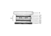
- a method of bonding the first clad film 11 to the core film 12 will be specifically described with reference to FIGS.
- the first clad film 11 obtained in the clad film preparation step is bonded onto the laminated substrate 71 via the protective sheet 72 and the clad film support base material 42.
- the surface of the laminated substrate 71 on which the first clad film 11 is not laminated is adsorbed and fixed to the adsorbing plate 73 of the bonding apparatus.
- the core film 12 whose surface wettability has been improved by corona treatment is also adsorbed and fixed to the adsorbing plate 73 of the laminating apparatus via the core film support base 41.
- thermocompression treatment for example, the core film 12 and the first clad film 11 are thermocompression bonded using a laminator made of silicon rubber 8.
- the temperature for thermocompression bonding is generally set in the range of 80 to 140 ° C., preferably 100 to 120 ° C.
- the pressure for thermocompression bonding is generally set in the range of 0.1 to 10 MPa, preferably 0.1 to 4 MPa.
- the laminated substrate 71 For example, a base material with high in-plane smoothness, such as a stainless plate, glass, Si wafer, a bake board, is used.
- the protective sheet 72 is not particularly limited, and for example, a sheet-like polymer film such as PET, PI, Teflon (registered trademark) is used.
- thermocompression bonding by applying a reduced pressure atmosphere or a vacuum as necessary, gas components such as air that can be entrained and remain between the first clad film 11 and the core film 12 at the time of lamination are minimized.
- the first clad film laminate 9 having excellent flatness can be obtained by suppressing the generation of voids at the contact portion.
- the reduced-pressure atmosphere or vacuum can be applied when the first clad film 11 and the core film 12 are in contact, when the first clad film 11 and the core film 12 are thermocompression bonded, or both.
- a reduced-pressure atmosphere or a vacuum can be applied by employing a vacuum lamination, a vacuum press, or the like.
- the adhesion force between the core film 12 and the first clad film 11 becomes the adhesion force between the core film 12 and the core film support substrate 41. Become stronger. As a result, peeling of the core film support base 41 from the core film 12 becomes easy. That is, if the adhesion between the core film 12 and the first clad film 11 is stronger than the adhesion between the core film 12 and the core film support base 41, the core film 12 is peeled off from the core film support base 41 when the core film 12 is peeled off. The film 12 does not peel from the first clad film 11.
- Adhesion of the core film 12 and the first cladding film 11 is more preferably preferably 100 ⁇ 1000gf / cm 2, a 200 ⁇ 800gf / cm 2.
- the adhesion strength of the core film 12 and the core film support substrate 41 is preferably 10 ⁇ 200gf / cm 2, more preferably 50 ⁇ 100gf / cm 2.
- the adhesion is measured according to JIS K7127.
- the obtained three-layer optical waveguide was cut into the shape of a test piece specified by JIS K7127, and both ends of this test piece were taken from a tensile tester (tensile tester Tensilon STM-T-50 manufactured by A & D Corporation). The test machine was operated while being held between the chuck portions and the crosshead speed was maintained at 5 cm / min, and the strength at which the test piece broke was measured.
- the adhesive force between the core film 12 and the first clad film 11 is equal to or greater than the above lower limit, an optical waveguide having high light propagation performance can be obtained. Moreover, if the adhesive force of the core film 12 and the 1st clad film 11 is below the said upper limit, the external formability of an optical waveguide structure will not be impaired. Furthermore, if the adhesive force between the core film 12 and the core film support base material 41 is within the above range, they are not naturally peeled during handling, and the core film support base material 41 is easily peeled off during the base material removal step. can do.
- Substrate removing step the core film supporting substrate 41 is removed from the core film 12.
- the method of removing the core film support base 41 from the core film 12 is, for example, by putting peeling flakes into the core film support base 41 with something like tweezers with a thin tip, and the core film support base 41 from the core film 12.
- a tape having a high adhesive force may be applied to the core film support base 41 and the tape may be peeled off together with the core film support base 41.
- the core film 12 is peeled off from the core film support base material 41, it is hardly laminated on the clad film 11, and therefore hardly receives the shrinkage stress of the core film support base material 41. For this reason, the dimensional change of the core film 12 produced at the time of lamination
- the surface of the core film 12 from which the core film supporting base material 41 is peeled from the first clad film laminated body 9 has a refractive index lower than that of the core portion 121.
- the second cladding film 13 is laminated.
- stacked is demonstrated.
- a method of bonding the second clad film 13 to the core film 12 will be specifically described with reference to FIGS.
- the second clad film 13 obtained in the clad film production step is adsorbed and fixed to the adsorbing plate 73 of the laminating apparatus via the clad film support base material 42.
- the surface of the core film 12 exposed by peeling the core film support substrate 41 from the first clad film laminate 9 was subjected to corona treatment to improve the surface wettability.
- the surface of the laminated substrate 71 on which the first clad film laminate 9 is laminated via the protective sheet 72 and not laminated with the first clad film laminate 9 is adsorbed and fixed to the adsorption plate 73 of the bonding apparatus. .
- thermocompression treatment the core film 12 and the second clad film 13 are thermocompression bonded using, for example, a laminator made of silicon rubber 8.
- the temperature for thermocompression bonding is generally set in the range of 80 to 140 ° C., preferably 100 to 120 ° C.
- the pressure for thermocompression bonding is generally set in the range of 0.1 to 10 MPa, preferably 0.1 to 4 MPa.
- thermocompression bonding by applying a reduced pressure atmosphere or a vacuum as necessary, gas components such as air that can be entrained and remain between the second clad film 13 and the core film 12 at the time of lamination are minimized. It is preferable that the optical waveguide structure 1 with good flatness can be obtained by suppressing the generation of voids at the contact portion.
- the reduced-pressure atmosphere or vacuum can be applied at the time of contact between the second clad film 13 and the core film 12, or at the time of thermocompression bonding of the second clad film 13 and the core film 12, or both.
- a reduced-pressure atmosphere or a vacuum can be applied by employing a vacuum lamination, a vacuum press, or the like.
- an optical waveguide can be obtained through the above-described steps, but further, treatment that improves environmental resistance such as heat resistance, moisture resistance, reflow resistance, flame resistance, and chemical resistance. It is preferable to carry out. It is also preferable to perform a treatment that improves mechanical resistance such as bending resistance, bending resistance, and tensile resistance. Examples of these treatments include a method of attaching a polyimide tape or a polyurethane tape to at least one side of the obtained optical waveguide.
- the process (aging process) of cooling the core film support base material 41 is performed between the first clad layer laminating step and the base material removing step. Cooling may be performed until the film surface temperature is lowered to around room temperature, preferably 15 to 25 ° C., more preferably 18 to 22 ° C.
- the cooling method used in the aging step is not particularly limited, and natural cooling may be used, and in the case of using equipment or the like, cooling may be performed using a sample cooling fan of a laminator, for example.
- the core film 12 and the first clad film 11 are sufficiently thermocompression bonded, and when the core film support base 41 is peeled from the core film 12, the core film 12 and the clad film 11 are separated. Generation of microvoids can be suppressed.
- the film surface temperature as much as possible, the structural change at the time of peeling is reduced as much as possible, and by suppressing the change in the dimensional and refractive index distribution, the optical waveguide structure having small dimensional change and in-plane variation in optical characteristics. Is obtained.
- a mold release process is performed on the surface of the core film support base 41 on the side on which the core film 12 is formed.
- the surface of the core film support base 41 on the side on which the core film 12 is formed is coated or ashed with a material having a low surface tension, specifically, Teflon (registered trademark) to improve the surface releasability.
- the core film supporting substrate 41 can be easily peeled from the core film 12 after the first clad film 11 is laminated by performing a mold release treatment on the core film supporting substrate 41.
- the surface smoothness of the core film support base material 41 can be improved by performing a mold release process on the core film support base material 41. That is, if the core film supporting substrate 41 has irregularities, the irregularities may be transferred to the core film 12 and light scattering may occur.
- the surface smoothness of the core film supporting substrate 41 can be improved by the release treatment. By improving, such light scattering can be suppressed.
- the surface smoothness of the core film support substrate 41 after the release treatment is reduced to 1/10 of the transmission wavelength with an arithmetic average roughness Ra, approximately 60 nm or less, the unevenness of the core film 12 Can suppress light scattering.
- the arithmetic average roughness Ra is measured according to JIS B0601. Specifically, the surface is scanned with a LASER microscope and the scattered light from the surface is measured. The arithmetic average roughness Ra is calculated by analyzing the measured light quantity.
- the optical waveguide obtained by the above-described method can be used for an optical wiring for optical communication, for example.
- this optical wiring can be combined with the existing electrical wiring on the substrate to constitute a so-called “photoelectric mixed substrate”.
- an optical signal transmitted through an optical wiring core portion of an optical waveguide
- an electric signal in an optical device is converted into an electric signal in an optical device and transmitted to the electric wiring.
- high-speed and large-capacity information transmission can be achieved in the optical wiring portion as compared with the conventional electric wiring.
- this opto-electric hybrid board may be mounted on an electronic device that transmits a large amount of data at high speed, such as a mobile phone, a game machine, a personal computer, a television, and a home server.
- Example 1 Preparation of core film ⁇ Synthesis of hexyl norbornene (HxNB) / diphenylmethylnorbornene methoxysilane (diPhNB) copolymer> HxNB (CAS number 22094-83-3) (9.63 g, 0.054 mol), diPhNB (CAS number 376634-34-3) (40.37 g, 0.126 mol), 1-hexene ( 4.54 g, 0.054 mol) and toluene (150 g) were mixed in a 500 mL sealam bottle in a dry box, and further stirred while heating to 80 ° C. in an oil bath to obtain a solution.
- HxNB hexyl norbornene
- diPhNB diphenylmethylnorbornene methoxysilane
- 1-hexene 4.54 g, 0.054 mol
- toluene 150 g
- the solid content was collected by filtration and vacuum dried in an oven at 60 ° C. to obtain a product having a dry mass of 19.0 g (yield 38%).
- Mw mass average molecular weight
- Mn number average molecular weight
- the product was measured by 1 H-NMR and identified as a HxNB / diPhNB-based copolymer.
- the refractive index of this copolymer was measured by the prism coupling method, the TE mode was 1.5695 and the TM mode was 1.5681 at a wavelength of 633 nm.
- the core film was irradiated with ultraviolet light through a mask having an opening to form a desired pattern, thereby obtaining a core film.
- thermocompression bonding conditions were 140 ° C., 0.3 MPa, and 210 s under vacuum conditions.
- ⁇ Substrate removal step> After the cooling step, a highly adhesive tape was applied to the PET film supporting the core film, and the PET film was peeled off from the core film together while peeling the tape.
- ⁇ Second cladding layer lamination step> The second clad film was adsorbed and fixed to the laminating apparatus via the PI film.
- the core film from which the PET film was peeled was subjected to corona treatment, and then adsorbed and fixed to the laminating apparatus via the first clad film, PI film, protective film, and laminated substrate in this order.
- the 2nd clad film and the core film were temporarily pasted over the automatic roller.
- a protective sheet was placed on the second clad film via the PI film, and the second clad film and the core film were thermocompression bonded by a laminator.
- the thermocompression bonding conditions were 140 ° C., 0.3 MPa, and 210 s under vacuum conditions.
- the prepared three-layer optical waveguide was fixed on a support base (stainless steel plate) with a magnet, placed in an oven, and cured at 160 ° C. for 2 hours.
- the regression line of the total light propagation loss data is expressed by the following equation.
- y mx + b
- m represents the light propagation loss
- b represents the coupling loss
- x represents the length of the optical waveguide
- y represents the total propagation light loss.
- the light propagation loss of the optical waveguide of Example 1 was 0.06 dB / cm.
- the surface arithmetic mean roughness was 50 nm.
- the arithmetic average roughness of the surface of the PET film coated with Teflon (registered trademark) was 30 nm.
- the obtained three-layer optical waveguide was cut into the shape of a test piece specified by JIS K7127.
- the both ends of the test piece are sandwiched between chuck portions of a tensile tester (tensile tester Tensilon STM-T-50 manufactured by A & D Co., Ltd.), and the crosshead speed is maintained at 5 cm / min. It was actuated and the strength at which the test piece broke was measured.
- the adhesion between the core film and the clad film of the optical waveguide of Example 1 was 500 gf / cm 2 or more.
- the adhesive force between the core film of the core forming film produced in Example 1 and the PET film was 50 gf / cm 2 .
- Example 2 The first cladding layer stacking step was the same as in Example 1 except that the following was performed.
- First cladding layer lamination step> The first clad film was adsorbed and fixed to the laminating apparatus through the PI film, the protective sheet, and the laminated substrate in this order.
- the core film was subjected to corona treatment and then adsorbed and fixed to a laminating apparatus via a PET film. Then, the 1st clad film and the core film were temporarily pasted over the automatic roller.
- thermocompression bonding conditions were 140 ° C., 0.3 MPa, and 210 s under vacuum conditions.
- the laminator air cooling device was not used, and it was immediately removed. Thereafter, a tape having high adhesive strength was applied to the support substrate (PET film) of the core film, and the support substrate was peeled off while peeling the tape.
- the optical propagation loss of the optical waveguide of Example 2 implemented in the same manner as described above was 0.10 dB / cm. Moreover, as a result of measuring the surface roughness of the core film, the surface arithmetic average roughness was 50 nm.
- Example 3 The core-forming film was produced in the same manner as in Example 1 except for the following. ⁇ Preparation of film for core formation> After 200 g of the core varnish is filled in the syringe of the coating machine, the core varnish is applied to the support substrate of the PET film (thickness 100 ⁇ m) with a nozzle capable of controlling discharge, and a uniform liquid with a thickness of 150 ⁇ m is applied to the support substrate. A core coating was formed. Then, this coating film was put into a dryer together with a PET film and heated at 45 ° C. for 20 minutes to evaporate mesitylene to obtain a dried coating film having a thickness of 40 ⁇ m.
- the optical propagation loss of the optical waveguide of Example 3 carried out in the same manner as described above was 0.20 dB / cm. Moreover, as a result of measuring the surface roughness of the core film, the surface arithmetic average roughness was 200 nm.
- Example 2 The production of the three-layer optical waveguide was performed in the same manner as in Example 1 except for the following. ⁇ Lamination of first clad film> The first clad film was adsorbed and fixed to the laminating apparatus. On the other hand, the core film was peeled off from the core support substrate, and then subjected to corona treatment, and was adsorbed and fixed to the laminating apparatus. Finally, the first clad film and the core film were temporarily attached by applying an automatic roller.
- the second clad film was adsorbed and fixed to the laminating apparatus.
- the core film on which the first clad film was laminated was subjected to corona treatment on the core film and fixed to the bonding apparatus by suction.
- the second clad film and the core film were temporarily attached by applying an automatic roller. Thereafter, protective sheets were placed on both sides, and thermocompression bonded with a laminator.
- the thermocompression bonding conditions were 140 ° C., 0.3 MPa, and 210 s under vacuum conditions.
- the optical propagation loss of the optical waveguide of the comparative example implemented in the same manner as described above was 0.06 dB / cm. Moreover, as a result of measuring the surface roughness of the core film, the surface arithmetic average roughness was 50 nm.
- the layers of the optical waveguide when the layers of the optical waveguide are laminated, the layers are laminated in a state of being fixed on the support base material. For this reason, the free expansion and contraction of each layer is restricted, and the dimensional change that occurs in the manufacturing process of the optical waveguide can be suppressed.
- Optical waveguide (optical waveguide structure) 11 First cladding layer (first cladding film) 12 Core layer (core film) 121 Core part 122 Clad part 13 Second clad layer (second clad film) 2 Core forming film 21 Core film forming material (core varnish) 31 Clad film forming material (clad varnish) 41 Core film support base 42 Cladding film support base 5 Nozzle 6 Mask 61 Chrome 71 Laminated substrate 72 Protective sheet 73 Suction plate 74 Automatic roller 8 Silicon rubber 9 First clad film laminated body
Landscapes
- Physics & Mathematics (AREA)
- Engineering & Computer Science (AREA)
- Microelectronics & Electronic Packaging (AREA)
- General Physics & Mathematics (AREA)
- Optics & Photonics (AREA)
- Optical Integrated Circuits (AREA)
Abstract
コア部と該コア部よりも屈折率の低いクラッド部とを備えるコア層と、前記コア層を挟んで配置される第1クラッド層及び第2クラッド層とを備える光導波路の製造方法は、基材に積層形成した前記コア層に前記第1クラッド層を積層する第1クラッド層積層工程と、前記コア層から前記基材を除去する基材除去工程と、前記コア層の前記基材を除去した側の面に前記第2クラッド層を積層する第2クラッド層積層工程と、をこの順に有する。
Description
本発明は、光導波路の製造方法に関する。
本願は、2010年12月14日に、日本に出願された特願2010-278178号に基づき優先権を主張し、その内容をここに援用する。
本願は、2010年12月14日に、日本に出願された特願2010-278178号に基づき優先権を主張し、その内容をここに援用する。
電子素子間や配線基板間の高速・高密度信号伝送において、従来の電気配線による伝送では、信号の相互干渉や減衰が障壁となり、高速・高密度化の限界が見え始めている。このため、電子素子間や配線基板間を光で接続する技術、いわゆる光インタコネクションが検討されている。光路としては、素子や基板との結合の容易さ、取り扱い易さの観点から、柔軟性を備えたフィルム状の光導波路が検討されている。
フィルム状光導波路と光デバイスの接続方法として、例えば光導波路をPMTコネクタ内部に組み込み、光デバイスとコネクタ勘合して接続する方法がある。このとき、コネクタ規格に適合するように外形加工を施すだけでなく、結合先のコネクタと光軸ズレがないように、コアピッチをコネクタ規格に適させる必要がある。
コアピッチは、マスク設計や描画精度により制御可能ではあるが、熱硬化収縮するようなフィルムであれば、その寸法変化率を踏まえた設計が必要になる。また、光導波路内に熱収縮率の違う構造体があれば、密着する層が相互に伸縮を及ぼし、その制御は極めて難しくなる。そこで、その熱応力を構造内部に溜め込むのではなく、例えば、熱膨張率の異なる構造体間に充分熱膨張係数が小さいスペーサーを、密着させないで噛ませ、熱応力を構造体とスペーサー間の滑りに変えるような構成にすれば、寸法変化を抑えられる可能性がある。(特許文献1参照)。
しかし、この方法では、応力を外力に変える構造体を形成する必要があるため、作業効率が悪いだけでなく、スペーサーの材質や重量により、変化率が変動する可能性があった。
本発明の目的は、製造時に生じる寸法変化を抑制した光導波路の製造方法を提供することにある。
このような目的は、下記(1)~(6)の本発明により達成される。
(1)コア部と該コア部よりも屈折率の低いクラッド部とを備えるコア層と、前記コア層を挟んで配置される第1クラッド層及び第2クラッド層とを備える光導波路の製造方法であって、基材に積層形成した前記コア層に前記第1クラッド層を積層する第1クラッド層積層工程と、前記コア層から前記基材を除去する基材除去工程と、前記コア層の前記基材を除去した側の面に前記第2クラッド層を積層する第2クラッド層積層工程と、をこの順に有する光導波路の製造方法。
(2)前記第1クラッド層積層工程と前記基材除去工程との間に、前記第1クラッド層、前記コア層及び前記基材を室温近傍まで冷却する工程を有する(1)に記載の光導波路の製造方法。
(3)前記基材の前記コア層を形成する側の面には離型処理がなされている(1)または(2)のいずれかに記載の光導波路の製造方法。
(4)前記離型処理を行った面は、表面粗さが算術平均粗さRaで60nm以下である(3)に記載の光導波路の製造方法。
(5)前記コア層と前記第1クラッド層の密着力が、前記コア層と前記基材の密着力よりも大きいことを特徴とする(1)から(4)のいずれかに記載の光導波路の製造方法。
(6)前記コア層と前記第1クラッド層の密着力が100から1000gf/cm2の間であり、前記コア層と前記基材の密着力が10から200gf/cm2の間であることを特徴とする(5)に記載の光導波路の製造方法。
(1)コア部と該コア部よりも屈折率の低いクラッド部とを備えるコア層と、前記コア層を挟んで配置される第1クラッド層及び第2クラッド層とを備える光導波路の製造方法であって、基材に積層形成した前記コア層に前記第1クラッド層を積層する第1クラッド層積層工程と、前記コア層から前記基材を除去する基材除去工程と、前記コア層の前記基材を除去した側の面に前記第2クラッド層を積層する第2クラッド層積層工程と、をこの順に有する光導波路の製造方法。
(2)前記第1クラッド層積層工程と前記基材除去工程との間に、前記第1クラッド層、前記コア層及び前記基材を室温近傍まで冷却する工程を有する(1)に記載の光導波路の製造方法。
(3)前記基材の前記コア層を形成する側の面には離型処理がなされている(1)または(2)のいずれかに記載の光導波路の製造方法。
(4)前記離型処理を行った面は、表面粗さが算術平均粗さRaで60nm以下である(3)に記載の光導波路の製造方法。
(5)前記コア層と前記第1クラッド層の密着力が、前記コア層と前記基材の密着力よりも大きいことを特徴とする(1)から(4)のいずれかに記載の光導波路の製造方法。
(6)前記コア層と前記第1クラッド層の密着力が100から1000gf/cm2の間であり、前記コア層と前記基材の密着力が10から200gf/cm2の間であることを特徴とする(5)に記載の光導波路の製造方法。
本発明によれば、光導波路の各層を積層するに際し、各層を支持基材上に固定した状態で積層する。このため、各層の自由な伸縮が規制され、光導波路の製造工程において生じる寸法変化を抑制することができる。
<光導波路>
以下、本発明の光導波路の構造について説明する。
図1は、本発明における光導波路の断面図である。
以下、本発明の光導波路の構造について説明する。
図1は、本発明における光導波路の断面図である。
図1に示すように光導波路1は、コア部121とコア部121より屈折率の低いクラッド部122とを有するコア層(以下、コアフィルムと呼ぶこともある)12と、コア層12を挟んで配置される第1クラッド層(以下、第1クラッドフィルムと呼ぶこともある)11及び第2クラッド層(以下、第2クラッドフィルムと呼ぶこともある)13(以下、第1クラッド層と第2クラッド層を合わせてクラッド層またはクラッドフィルムと呼ぶこともある)と、を備える。コア部121は、伝送光の光路を形成する部分であり、クラッド部122は、コア層12に形成されているものの伝送光の光路を形成せず、クラッド層11、13と同様の機能を果たす部分である。
コア層12の厚さは、形成すべき光導波路1の厚さに応じて適宜設定され、特に限定されないが、1μm以上200μm以下であるのが好ましく、5μm以上100μm以下であるのがより好ましく、10μm以上60μm以下であるのがさらに好ましい。
コア層12の構成材料としては、光(例えば紫外線)の照射により、あるいはさらに加熱することにより屈折率が変化する材料が用いられる。このような材料の好ましい例としては、ベンゾシクロブテン系ポリマー、ノルボルネン系ポリマー等の環状オレフィン系樹脂を含む樹脂組成物を主材料とするものが挙げられ、ノルボルネン系ポリマーを含む(主材料とする)ものが特に好ましい。
このような材料で構成されたコア層12は、曲げ等の変形に対する耐性に優れ、特に繰り返し湾曲変形した場合でも、コア部121とクラッド部122との剥離や、コア層12と隣接するクラッド層11、13との層間剥離が生じ難く、コア部121、クラッド部122内にマイクロクラックが発生することも防止される。その結果、光導波路1の光伝送性能が維持され、耐久性に優れた光導波路1が得られる。
また、コア層12の構成材料には、例えば、酸化防止剤、屈折率調整剤、可塑剤、増粘剤、補強剤、増感剤、レベリング剤、消泡剤、密着助剤および難燃剤等の添加剤が含まれていてもよい。酸化防止剤の添加は、高温安定性の向上、耐候性の向上、光劣化の抑制という効果がある。このような酸化防止剤としては、例えば、モノフェノール系、ビスフェノール系、トリフェノール系等のフェノール系や、芳香族アミン系のものが挙げられる。また、可塑剤、増粘剤、補強剤の添加により、曲げに対する耐性をさらに増大させることもできる。
前記酸化防止剤に代表される添加剤の含有率(2種以上の場合は合計)は、コア層12の構成材料全体に対し、0.5~40重量%程度が好ましく、3~30重量%程度がより好ましい。この量が少なすぎると、添加剤の機能を十分に発揮することができず、量が多すぎると、添加剤の種類や特性によっては、コア部121を伝送する光(伝送光)の透過率の低下、パターニング不良、屈折率不安定等を生じるおそれがある。
形成されるコア部121のパターン形状としては、特に限定されず、直線状、湾曲部を有する形状、異形、光路の分岐部、合流部または交差部を有する形状、集光部(幅等が減少している部分)または光拡散部(幅等が増大している部分)、あるいはこれらのうちの2以上を組み合わせた形状等、いかなるものでもよい。光の照射パターンの設定により、いかなる形状のコア部121をも容易に形成することができる。
クラッド層11、13の厚さは、形成すべき光導波路1の厚さに応じて適宜設定され、特に限定されないが、0.1μm以上100μm以下であるのが好ましく、1μm以上50μm以下であるのがより好ましく、5μm以上30μm以下であるのがさらに好ましい。
クラッド層11、13の構成材料としては、コア層12のコア部121より低屈折率の材料が用いられる。例えば、アクリル系樹脂、メタクリル系樹脂、ポリカーボネート、ポリスチレン、エポキシ樹脂、ポリアミド、ポリイミド、ポリベンゾオキサゾール、ベンゾシクロブテン系樹脂やノルボルネン系樹脂等の環状オレフィン系樹脂等が挙げられ、これらのうちの1種または2種以上を組み合せて(ポリマーアロイ、ポリマーブレンド(混合物)、共重合体、複合体(積層体)など)用いることができる。
これらのうち、特に耐熱性に優れるという点で、エポキシ樹脂、ポリイミド、ポリベンゾオキサゾール、ベンゾシクロブテン系樹脂やノルボルネン系樹脂等の環状オレフィン系樹脂、またはそれらを含むもの(主とするもの)を用いるのが好ましく、特に、ノルボルネン系樹脂(ノルボルネン系ポリマー)を主とするものが好ましい。
ノルボルネン系ポリマーは、耐熱性に優れるため、これをクラッド層11、13の構成材料として使用してなる光導波路では、光導波路に導体層を形成する際、導体層を加工して配線を形成する際、光学素子を実装する際、等に加熱されたとしても、クラッド層11、13が軟化して変形するのを防止することができる。
また、高い疎水性を有するため、吸水による寸法変化等を生じ難いクラッド層11、13を得ることができる。
また、ノルボルネン系ポリマーまたはその原料であるノルボルネン系モノマーは、比較的安価であり、入手が容易であることからも好ましい。
また、高い疎水性を有するため、吸水による寸法変化等を生じ難いクラッド層11、13を得ることができる。
また、ノルボルネン系ポリマーまたはその原料であるノルボルネン系モノマーは、比較的安価であり、入手が容易であることからも好ましい。
さらに、クラッド層11、13の構成材料として、ノルボルネン系ポリマーを主とするものを用いると、曲げ等の変形に対する耐性(耐屈曲性)に優れ、繰り返し屈曲変形させた場合でも、クラッド層11、13とコア層12との層間剥離が生じ難く、クラッド部122の内部にマイクロクラックが発生することも防止される。このようなことから、光導波路1の光伝送性能が維持され、最終的に耐久性に優れた光導波路1が得られる。
クラッド層11、13は、コア層12を挟んで配置されるが、それぞれのクラッド層は同種の構成材料から成ってもよいし、異なる構成材料から成ってもよい。
なお、図1に示す光導波路1は、2つのコア部121を有するものであるが、1つの光導波路1に形成されるコア部121の数は、特に限定されるものではない。
さらに、図1では、コア層12は1層のみであるが、コア層12の数は特に限定されるものではなく、コア層12が複数積層されていてもよい。
さらに、図1では、コア層12は1層のみであるが、コア層12の数は特に限定されるものではなく、コア層12が複数積層されていてもよい。
<光導波路の製造方法>
(第1実施形態)
次に、本発明の光導波路の製造方法の第1実施形態について説明する。
図2から図8は本発明における光導波路の製造方法の各工程を示した図である。
以下、光導波路の製造方法を、[1]コアフィルム作製工程、[2]クラッドフィルム作製工程、[3]第1クラッド層積層工程、[4]基材除去工程、[5]第2クラッド層積層工程、に分けて説明する。
(第1実施形態)
次に、本発明の光導波路の製造方法の第1実施形態について説明する。
図2から図8は本発明における光導波路の製造方法の各工程を示した図である。
以下、光導波路の製造方法を、[1]コアフィルム作製工程、[2]クラッドフィルム作製工程、[3]第1クラッド層積層工程、[4]基材除去工程、[5]第2クラッド層積層工程、に分けて説明する。
[1]コアフィルム作製工程
コアフィルム12を作製する工程では、屈折率の高いコア部121を有するコアフィルム12を作製する。例えば図3(a)に示すように、コアフィルム12は、コアフィルム支持基材41上に形成したコア形成用フィルム2に対して光を照射することで作製される。
コアフィルム12を作製する工程では、屈折率の高いコア部121を有するコアフィルム12を作製する。例えば図3(a)に示すように、コアフィルム12は、コアフィルム支持基材41上に形成したコア形成用フィルム2に対して光を照射することで作製される。
コア形成用フィルム2の構成材料には、伝搬する光に対して実質的に透明な材料であればいかなる材料をも用いることができ、具体的には、コア層12の構成材料として前述したものを用いることができる。
特に、コア形成用フィルム2は、例えば、600~1550nm程度の波長領域の光を使用したデータ通信において好適に使用される。したがって、この波長域にて十分な透明性を有するものが好適に用いられる。ここで、600~1550nm程度の波長領域で透明性を有するとは、例えば前記波長領域における光線透過率が90%以上であることが好ましく、特に99%以上であることが好ましい。ここで、光線透過率は、JIS K7105に従って測定される。具体的には、JIS K7105に準じたサイズにフィルムを形成、切り出す。分光計にセットして、フィルムに白色光源を透過させたのち、光線透過量を測定する。
特に、コア形成用フィルム2は、例えば、600~1550nm程度の波長領域の光を使用したデータ通信において好適に使用される。したがって、この波長域にて十分な透明性を有するものが好適に用いられる。ここで、600~1550nm程度の波長領域で透明性を有するとは、例えば前記波長領域における光線透過率が90%以上であることが好ましく、特に99%以上であることが好ましい。ここで、光線透過率は、JIS K7105に従って測定される。具体的には、JIS K7105に準じたサイズにフィルムを形成、切り出す。分光計にセットして、フィルムに白色光源を透過させたのち、光線透過量を測定する。
上述したような構成材料を用いてコア形成用フィルム2を形成する方法としては、例えば図2に示すように、コアフィルム形成用材料(以下、コアワニスと呼ぶこともある)21を、コアフィルム支持基材41に塗布した後、硬化(固化)させる方法により形成される。
具体的には、コアフィルム支持基材41上にコアフィルム形成用材料21を吐出制御可能なノズル5により塗布して、コアフィルム支持基材41上に液状被膜を形成する。この際、コアフィルム支持基材41は図2中のA方向に回転しており、ノズル5は、コアフィルム支持基材41の中央部から、B方向に移動するようになっている。また、ノズル5からのコアフィルム形成用材料21の吐出量は制御可能となっており、通常は、コアフィルム支持基材41の中央部から端部に向かうにつれて吐出量が多くなるように設定されている。これにより、コアフィルム支持基材41上にコアフィルム形成用材料21を均一の厚さで塗布することが可能となる。
コアフィルム支持基材41の回転数は、コア形成用フィルム2の厚さを制御する因子の一つであり、遠心力で塗布したコアフィルム形成用材料21が飛散しない回転数であればよく、具体的には60~100rpmが好ましい。
また、ノズル5からのコアフィルム形成用材料21の吐出量も、コア形成用フィルム2の厚さを制御する因子の一つであり、ノズル5とコアフィルム支持基材41のギャップが埋まる程度が良く、特に限定されないが、好ましくは3~7cc/minである。
また、ノズル5からのコアフィルム形成用材料21の吐出量も、コア形成用フィルム2の厚さを制御する因子の一つであり、ノズル5とコアフィルム支持基材41のギャップが埋まる程度が良く、特に限定されないが、好ましくは3~7cc/minである。
次に、このコアフィルム形成用材料21が塗布されたコアフィルム支持基材41を換気されたレベルテーブルに置いて、液状被膜表面の不均一な部分を水平化するとともに、溶媒を蒸発(脱溶媒)する。これにより、コア形成用フィルム2を得ることができる。乾燥条件は、特に限定されないが、40~50℃で10~30分間行うことが好ましい。
コア形成用フィルム2を塗布法で形成する場合、上述した方法以外にも、例えばドクターブレード法、スピンコート法、ディッピング法、テーブルコート法、スプレー法、アプリケーター法、カーテンコート法、ダイコート法等の方法が挙げられるが、これらに限定されるわけではない。
コアフィルム支持基材41としては、例えばシリコン基板、二酸化ケイ素基板、ガラス基板、石英基板、ポリエチレンテレフタレート(PET)フィルム等が用いられる。
このようなコア形成用フィルム2の平均厚さは、形成すべきコアフィルム12の厚さに応じて適宜設定され、特に限定されないが、1~200μm程度であるのが好ましく、5~100μm程度であるのがより好ましく、10~60μm程度であるのがさらに好ましい。
また、コアフィルム12とクラッドフィルム11、13との界面でそれぞれ全反射を生じさせるために、界面に屈折率差が存在する必要がある。このため、コア形成用フィルム2の屈折率は、クラッドフィルム11、13の屈折率より高ければ良く、特に限定されないが、好ましくはクラッドフィルム11、13の屈折率の1.5~1.8程度とされる。
次に、コア形成用フィルム2に対し、選択的に光(たとえば、紫外線)を照射し、コアフィルム12を形成する工程を説明する。
本工程では、図3(a)に示すように、コア形成用フィルム2の上方に、クロム61により形成されたマスク6を配置する。このマスク6の開口を介して、コア形成用フィルム2に対し、光を照射する。
本工程では、図3(a)に示すように、コア形成用フィルム2の上方に、クロム61により形成されたマスク6を配置する。このマスク6の開口を介して、コア形成用フィルム2に対し、光を照射する。
照射される光としては、可視光、紫外光、赤外光、レーザー等の活性エネルギー光線が挙げられる。また、光以外にも、X線等の電磁波や、電子線等の粒子線を照射するようにしても良い。特に、波長200~450nmの範囲にピーク波長を有するものを用いることで、光酸発生剤の組成にもよるが、光酸発生剤を比較的容易に活性化させることができる。
また、光の照射量は、特に限定されないが、0.1~9J/cm2程度であるのが好ましく、0.2~6J/cm2程度であるのがより好ましく、0.2~3J/cm2程度であるのがさらに好ましい。
なお、レーザー光のように指向性の高い光を用いる場合には、マスク6の使用を省略することもできる。
次に、光照射されたコア形成用フィルム2をオーブン(好ましくは120~160℃、10~30分間)で硬化させる。その結果、光が照射された部位は、酸による低屈折率成分の重合及び高屈折率成分の乖離作用により屈折率が低下し、光が照射されなかった部位との間で屈折率の差が生じる。また、熱をかけることでより一層屈折率の差を発現できる。その結果、コア形成用フィルム2の光が照射された部位がクラッド部122となり、照射されなかった部位がコア部121となる。これにより、コアフィルム12が形成される(図3(b))。
[2]クラッドフィルム作製工程
クラッドフィルム11、13の形成用材料としては、伝搬する光に対して実質的に透明な材料であればいかなる材料をも用いることができ、クラッド層11、13の構成材料として前述したものを用いることができる。 特に、クラッドフィルム11、13は、例えば、600~1550nm程度の波長領域の光を使用したデータ通信において好適に使用されるので、この波長域にて十分な透明性を有するものがクラッドフィルム11、13の形成用材料として好適に用いられる。ここで、600~1550nm程度の波長領域で透明性を有するとは、例えば前記波長領域における光線透過率が90%以上であることが好ましく、特に99%以上であることが好ましい。
クラッドフィルム11、13の形成用材料としては、伝搬する光に対して実質的に透明な材料であればいかなる材料をも用いることができ、クラッド層11、13の構成材料として前述したものを用いることができる。 特に、クラッドフィルム11、13は、例えば、600~1550nm程度の波長領域の光を使用したデータ通信において好適に使用されるので、この波長域にて十分な透明性を有するものがクラッドフィルム11、13の形成用材料として好適に用いられる。ここで、600~1550nm程度の波長領域で透明性を有するとは、例えば前記波長領域における光線透過率が90%以上であることが好ましく、特に99%以上であることが好ましい。
クラッドフィルム作製工程において、クラッドフィルム11、13は、コア形成用フィルム2と同様の方法で作製することができる。すなわち、図4に示すように、クラッドフィルム支持基材42上にクラッドフィルム形成用材料(以下、クラッドワニスと呼ぶこともある)31を吐出制御可能なノズル5により塗布して、クラッドフィルム支持基材42上に液状被膜を形成する。
クラッドフィルム支持基材42としては、コアフィルム支持基材41と同様の材料を用いることができ、例えば、シリコン基板、二酸化ケイ素基板、ガラス基板、石英基板、ポリエチレンテレフタレート(PET)フィルム等が用いられる。
クラッドフィルム支持基材42は図4中のA方向に回転しており、ノズル5は、クラッドフィルム支持基材42の中央部より、B方向に移動するようになっている。この際、ノズル5からのクラッドフィルム形成用材料31の吐出量は制御可能となっており、通常は、クラッドフィルム支持基材42の中央部から端部に向かうにつれて吐出量が多くなるように設定されている。これにより、クラッドフィルム支持基材42上にクラッドフィルム形成用材料31を均一の厚さで塗布することが可能となる。
クラッドフィルム支持基材42の回転数は、クラッドフィルム11、13の厚さを制御する因子の一つであり、遠心力で塗布したクラッドフィルム形成用材料31が飛散しない回転数であればよく、具体的には60~100rpmが好ましい。
また、ノズル5からのクラッドフィルム形成用材料31の吐出量も、クラッドフィルム11、13の厚さを制御する因子の一つであり、ノズル5とクラッドフィルム支持基材42のギャップが埋まる程度が良く、特に限定されないが、好ましくは3~7cc/minである。
また、ノズル5からのクラッドフィルム形成用材料31の吐出量も、クラッドフィルム11、13の厚さを制御する因子の一つであり、ノズル5とクラッドフィルム支持基材42のギャップが埋まる程度が良く、特に限定されないが、好ましくは3~7cc/minである。
次に、このクラッドフィルム形成用材料31が塗布されたクラッドフィルム支持基材42を換気されたレベルテーブルに置いて、液状被膜表面の不均一な部分を水平化するとともに、溶媒を蒸発(脱溶媒)する。これにより、クラッドフィルム11、13を得ることができる。乾燥条件は、特に限定されないが、40~50℃で10~30分間行うことが好ましい。
クラッドフィルム11、13を塗布法で形成する場合、上述した方法以外にも、例えばドクターブレード法、スピンコート法、ディッピング法、テーブルコート法、スプレー法、アプリケーター法、カーテンコート法、ダイコート法等の方法が挙げられるが、これらに限定されるわけではない。
このようなクラッドフィルム11、13の平均厚さは、形成すべきクラッドフィルム11、13の厚さに応じて適宜設定され、特に限定されないが、0.1~100μm程度であるのが好ましく、1~50μm程度であるのがより好ましく、5~30μm程度であるのがさらに好ましい。
[3]第1クラッド層積層工程
第1クラッドフィルム11を積層する工程では、コアフィルム12の一方の面に、コア部121よりも屈折率の低い第1クラッドフィルム11を積層する。
以下で、第1クラッドフィルム11を熱圧着によりコアフィルム12に積層する方法について説明する。
第1クラッドフィルム11を積層する工程では、コアフィルム12の一方の面に、コア部121よりも屈折率の低い第1クラッドフィルム11を積層する。
以下で、第1クラッドフィルム11を熱圧着によりコアフィルム12に積層する方法について説明する。
第1クラッドフィルム11をコアフィルム12に貼り合わせる方法について、図5、図6を用いて具体的に説明する。
前記クラッドフィルム作製工程で得られた第1クラッドフィルム11は、積層基板71上に、保護シート72とクラッドフィルム支持基材42を介して貼り合わせる。次いで、積層基板71の第1クラッドフィルム11が積層されていない側の面を、貼り合わせ装置の吸着板73に吸着固定する。
一方、コロナ処理をかけて表面の濡れ性が向上したコアフィルム12も、コアフィルム支持基材41を介して、貼り合わせ装置の吸着板73に吸着固定する。
次いで、自動ローラー74をかけて、第1クラッドフィルム11とコアフィルム12とを仮貼りさせる。
次いで、吸着板73を外し、コアフィルム支持基材41のコアフィルム12が積層されていない側の面に、保護シート72を載せて、熱圧着処理を施す。熱圧着処理では、例えば、シリコンラバー8によるラミネーターを用いて、コアフィルム12と第1クラッドフィルム11を熱圧着させる。熱圧着の温度としては、一般に80~140℃、好ましくは100~120℃の範囲に設定すればよい。熱圧着の圧力としては、一般に0.1~10MPa、好ましくは0.1~4MPaの範囲に設定すればよい。
前記クラッドフィルム作製工程で得られた第1クラッドフィルム11は、積層基板71上に、保護シート72とクラッドフィルム支持基材42を介して貼り合わせる。次いで、積層基板71の第1クラッドフィルム11が積層されていない側の面を、貼り合わせ装置の吸着板73に吸着固定する。
一方、コロナ処理をかけて表面の濡れ性が向上したコアフィルム12も、コアフィルム支持基材41を介して、貼り合わせ装置の吸着板73に吸着固定する。
次いで、自動ローラー74をかけて、第1クラッドフィルム11とコアフィルム12とを仮貼りさせる。
次いで、吸着板73を外し、コアフィルム支持基材41のコアフィルム12が積層されていない側の面に、保護シート72を載せて、熱圧着処理を施す。熱圧着処理では、例えば、シリコンラバー8によるラミネーターを用いて、コアフィルム12と第1クラッドフィルム11を熱圧着させる。熱圧着の温度としては、一般に80~140℃、好ましくは100~120℃の範囲に設定すればよい。熱圧着の圧力としては、一般に0.1~10MPa、好ましくは0.1~4MPaの範囲に設定すればよい。
前記積層基板71として、特に限定されないが、例えば、ステンレス板、ガラス、Siウェハ、ベーク板など面内平滑性の高い基材が用いられる。
また、保護シート72として、特に限定されないが、例えば、PET、PI、テフロン(登録商標)などのシート状ポリマーフィルムが用いられる。
また、保護シート72として、特に限定されないが、例えば、PET、PI、テフロン(登録商標)などのシート状ポリマーフィルムが用いられる。
上述の熱圧着に際しては、必要に応じて、減圧雰囲気または真空を適用することにより、積層時に第1クラッドフィルム11とコアフィルム12の間に連行されて残留し得る空気等の気体成分を最小限に抑えることができ、接触部におけるボイドの発生を抑え、平坦性の良好な第1クラッドフィルム積層体9を得ることができる上で好ましい。減圧雰囲気または真空は、第1クラッドフィルム11とコアフィルム12の接触時に、もしくは第1クラッドフィルム11とコアフィルム12の熱圧着時に、またはこれらの両方に、適用することができる。減圧雰囲気または真空の適用は、真空ラミネート、真空プレス等を採用することにより可能である。
上述の熱圧着時の熱によるコアフィルム12と第1クラッドフィルム11の架橋構造形成により、コアフィルム12と第1クラッドフィルム11の密着力が、コアフィルム12とコアフィルム支持基材41の密着力より強くなる。この結果、コアフィルム支持基材41のコアフィルム12からの剥離は容易になる。すなわち、コアフィルム12と第1クラッドフィルム11の密着力が、コアフィルム12とコアフィルム支持基材41の密着力より強ければ、コアフィルム12をコアフィルム支持基材41から剥離する際に、コアフィルム12が第1クラッドフィルム11から剥離することがない。
コアフィルム12と第1クラッドフィルム11の密着力は、100~1000gf/cm2が好ましく、200~800gf/cm2であることがより好ましい。また、コアフィルム12とコアフィルム支持基材41の密着力は、10~200gf/cm2が好ましく、50~100gf/cm2がより好ましい。ここで密着力はJIS K7127に従い測定される。得られた3層光導波路を、JIS K7127指定の試験片の形状に切り出し、この試験片の両端部を引っ張り試験機(エー・アンド・ディ株式会社製引っ張り試験機テンシロンSTM-T-50)のチャック部に挟み、そしてクロスヘッド速度を5cm/minに保ちながら試験機を作動させて、試験片が破断するときの強度を測定した。
コアフィルム12と第1クラッドフィルム11の密着力が上記下限以上であれば、光伝搬性能の高い光導波路を得ることができる。また、コアフィルム12と第1クラッドフィルム11の密着力が上記上限以下であれば、光導波路構造体の外形加工性を損なうことがない。さらに、コアフィルム12とコアフィルム支持基材41の密着力が上記範囲内であれば、ハンドリング時にこれらが自然剥離することなく、また基材除去工程においてはコアフィルム支持基材41を容易に剥離することができる。
[4]基材除去工程
基材除去工程において、コアフィルム12からコアフィルム支持基材41を除去する。コアフィルム12から、コアフィルム支持基材41を除去する方法は、例えば、先端の細いピンセットのようなもので剥離キッカケをコアフィルム支持基材41にいれて、コアフィルム12からコアフィルム支持基材41を剥離するだけでなく、コアフィルム支持基材41に粘着力の高いテープを貼りコアフィルム支持基材41と共にテープを剥がすだけでもよい。コアフィルム12は、コアフィルム支持基材41からは剥離するものの、クラッドフィルム11に積層されているので、コアフィルム支持基材41の収縮応力をほとんど受けない。このため、第1クラッドフィルム11とコアフィルム12の積層時に生じるコアフィルム12の寸法変化を抑制することができる。
基材除去工程において、コアフィルム12からコアフィルム支持基材41を除去する。コアフィルム12から、コアフィルム支持基材41を除去する方法は、例えば、先端の細いピンセットのようなもので剥離キッカケをコアフィルム支持基材41にいれて、コアフィルム12からコアフィルム支持基材41を剥離するだけでなく、コアフィルム支持基材41に粘着力の高いテープを貼りコアフィルム支持基材41と共にテープを剥がすだけでもよい。コアフィルム12は、コアフィルム支持基材41からは剥離するものの、クラッドフィルム11に積層されているので、コアフィルム支持基材41の収縮応力をほとんど受けない。このため、第1クラッドフィルム11とコアフィルム12の積層時に生じるコアフィルム12の寸法変化を抑制することができる。
[5]第2クラッド層積層工程
第2クラッド層積層工程では、第1クラッドフィルム積層体9からコアフィルム支持基材41を剥離したコアフィルム12の面に、コア部121よりも屈折率の低い第2クラッドフィルム13を積層する。
以下で、第2クラッドフィルム13を、コアフィルム12の第1クラッドフィルム11が積層されていない側の面上に積層する方法について説明する。
第2クラッド層積層工程では、第1クラッドフィルム積層体9からコアフィルム支持基材41を剥離したコアフィルム12の面に、コア部121よりも屈折率の低い第2クラッドフィルム13を積層する。
以下で、第2クラッドフィルム13を、コアフィルム12の第1クラッドフィルム11が積層されていない側の面上に積層する方法について説明する。
第2クラッドフィルム13をコアフィルム12に貼り合わせる方法について、図7、8を用いて具体的に説明する。
前記クラッドフィルム作製工程で得られた第2クラッドフィルム13は、クラッドフィルム支持基材42を介して、貼り合わせ装置の吸着板73に吸着固定する。
一方、第1クラッドフィルム積層体9からコアフィルム支持基材41を剥離し露出したコアフィルム12の面に、コロナ処理をかけて表面の濡れ性を向上させた。次いで、第1クラッドフィルム積層体9が保護シート72を介して積層されている積層基板71の第1クラッドフィルム積層体9が積層されていない面を、貼り合わせ装置の吸着板73に吸着固定する。
次いで、自動ローラー74をかけて、コアフィルム12と第2クラッドフィルム13とを仮貼りさせる。
次いで、吸着板73を外し、クラッドフィルム支持基材42を介して、第2クラッドフィルム13に保護シート72を新たに載せて、熱圧着処理を施す。熱圧着処理では、例えばシリコンラバー8によるラミネーターを用いて、コアフィルム12と第2クラッドフィルム13とを熱圧着させる。熱圧着の温度としては、一般に80~140℃、好ましくは100~120℃の範囲に設定すればよい。熱圧着の圧力としては、一般に0.1~10MPa、好ましくは0.1~4MPaの範囲に設定すればよい。
前記クラッドフィルム作製工程で得られた第2クラッドフィルム13は、クラッドフィルム支持基材42を介して、貼り合わせ装置の吸着板73に吸着固定する。
一方、第1クラッドフィルム積層体9からコアフィルム支持基材41を剥離し露出したコアフィルム12の面に、コロナ処理をかけて表面の濡れ性を向上させた。次いで、第1クラッドフィルム積層体9が保護シート72を介して積層されている積層基板71の第1クラッドフィルム積層体9が積層されていない面を、貼り合わせ装置の吸着板73に吸着固定する。
次いで、自動ローラー74をかけて、コアフィルム12と第2クラッドフィルム13とを仮貼りさせる。
次いで、吸着板73を外し、クラッドフィルム支持基材42を介して、第2クラッドフィルム13に保護シート72を新たに載せて、熱圧着処理を施す。熱圧着処理では、例えばシリコンラバー8によるラミネーターを用いて、コアフィルム12と第2クラッドフィルム13とを熱圧着させる。熱圧着の温度としては、一般に80~140℃、好ましくは100~120℃の範囲に設定すればよい。熱圧着の圧力としては、一般に0.1~10MPa、好ましくは0.1~4MPaの範囲に設定すればよい。
上述の熱圧着に際しては、必要に応じて、減圧雰囲気または真空を適用することにより、積層時に第2クラッドフィルム13とコアフィルム12の間に連行されて残留し得る空気等の気体成分を最小限に抑えることができ、接触部におけるボイドの発生を抑え、平坦性の良好な光導波路構造体1を得ることができる上で好ましい。減圧雰囲気または真空は、第2クラッドフィルム13とコアフィルム12の接触時に、もしくは第2クラッドフィルム13とコアフィルム12の熱圧着時に、またはこれらの両方に、適用することができる。減圧雰囲気または真空の適用は、真空ラミネート、真空プレス等を採用することにより可能である。
このようにして、上述のような工程を経て光導波路を得ることができるが、さらに、耐熱性、耐湿性、耐リフロー性、耐難燃性、耐薬品性といった環境耐性が向上するような処理を行うことが好ましい。また、耐曲げ性、耐屈曲性、耐引っ張り性といった機械耐性が向上するような処理を行うことも好ましい。これらの処理は、例えばポリイミドテープやポリウレタンテープを、得られた光導波路の少なくとも片面側に貼り付ける方法が挙げられる。
(第2実施形態)
次に、本発明の光導波路の製造方法の第2実施形態について説明する。
以下では第1実施形態との相違点を中心に説明し、同様の事項については、その説明を省略する。
次に、本発明の光導波路の製造方法の第2実施形態について説明する。
以下では第1実施形態との相違点を中心に説明し、同様の事項については、その説明を省略する。
第2実施形態では、第1クラッド層積層工程と基材除去工程との間、具体的には、第1クラッドフィルム11とコアフィルム12の熱圧着後に、第1クラッドフィルム11、コアフィルム12、およびコアフィルム支持基材41を冷却する工程(エージング工程)を行う。冷却はフィルム表面温度が室温近傍に下がるまで行えばよく、好ましくは15~25℃、より好ましくは18~22℃まで冷却すればよい。エージング工程で使用される冷却方法は特に限定されず、自然冷却でもよいし、機器等を用いる場合には例えばラミネーターのサンプル冷却用ファン等を用いて冷却を行ってもよい。
冷却工程(エージング工程)を行うことでコアフィルム12と第1クラッドフィルム11が充分に熱圧着され、コアフィルム12からコアフィルム支持基材41を剥離する際に、コアフィルム12とクラッドフィルム11にマイクロボイド発生を抑制することができる。また、フィルム表面温度を下げることで、剥離の際の構造変化を限りなく小さくし、寸法及び屈折率分布の変化を抑制することで、寸法変化と光学特性の面内バラツキが小さい光導波路構造体が得られる。
(第3実施形態)
次に、本発明の光導波路の製造方法の第3実施形態について説明する。
以下では第1実施形態との相違点を中心に説明し、同様の事項については、その説明を省略する。
次に、本発明の光導波路の製造方法の第3実施形態について説明する。
以下では第1実施形態との相違点を中心に説明し、同様の事項については、その説明を省略する。
第3実施形態では、コアフィルム支持基材41のコアフィルム12を形成する側の面に離形処理を行う。例えば、コアフィルム支持基材41のコアフィルム12を形成する側の面上に表面張力の弱い材料、具体的にはテフロン(登録商標)をコーティングまたはアッシング処理して、表面の離形性を向上させる。
コアフィルム支持基材41に離型処理を行うことで、第1クラッドフィルム11を積層したのちに、コアフィルム12から容易にコアフィルム支持基材41を剥離することができる。
また、コアフィルム支持基材41に離型処理を行うことでコアフィルム支持基材41の表面平滑性を向上させることができる。すなわち、コアフィルム支持基材41に凹凸があると、この凹凸がコアフィルム12に転写され、光散乱が発生する可能性があるが、離型処理によりコアフィルム支持基材41の表面平滑性を向上させることで、このような光散乱を抑制することができる。具体的には、離型処理後のコアフィルム支持基材41の表面平滑性を、算術平均粗さRaで伝送波長の10分の1、およそ60nm以下にまで低減させると、コアフィルム12の凹凸による光散乱が抑制できる。算術平均粗さRaは、JIS B0601に従い測定される。具体的には、LASER顕微鏡で表面を走査し、表面からの散乱光を計測。計測した光量の解析により、算術平均粗さRaを算出する。
上述の方法で得られた光導波路は、例えば光通信用の光配線に用いることができる。
また、この光配線は、既存の電気配線とともに基板上に混載されることにより、いわゆる「光電気混載基板」を構成することができる。かかる光電気混載基板では、例えば、光配線(光導波路のコア部)で伝送された光信号を、光デバイスにおいて電気信号に変換し、電気配線に伝達する。これにより、光配線の部分で、従来の電気配線よりも高速かつ大容量の情報伝送が可能になる。したがって、例えばCPUやLSI等の演算装置とRAM等の記憶装置との間をつなぐバス等に、この光電気混載基板を適用することにより、システム全体の性能を高めるとともに、電磁ノイズの発生を抑制することができる。
なお、かかる光電気混載基板は、例えば、携帯電話、ゲーム機、パソコン、テレビ、ホーム・サーバー等、大容量のデータを高速に伝送する電子機器類に搭載することが考えられる。
また、この光配線は、既存の電気配線とともに基板上に混載されることにより、いわゆる「光電気混載基板」を構成することができる。かかる光電気混載基板では、例えば、光配線(光導波路のコア部)で伝送された光信号を、光デバイスにおいて電気信号に変換し、電気配線に伝達する。これにより、光配線の部分で、従来の電気配線よりも高速かつ大容量の情報伝送が可能になる。したがって、例えばCPUやLSI等の演算装置とRAM等の記憶装置との間をつなぐバス等に、この光電気混載基板を適用することにより、システム全体の性能を高めるとともに、電磁ノイズの発生を抑制することができる。
なお、かかる光電気混載基板は、例えば、携帯電話、ゲーム機、パソコン、テレビ、ホーム・サーバー等、大容量のデータを高速に伝送する電子機器類に搭載することが考えられる。
以下、本発明を実施例に基づいてより詳細に説明するが、本発明はこれに限定されるものではない。
(実施例1)
1.コアフィルムの作製
<ヘキシルノルボルネン(HxNB)/ジフェニルメチルノルボルネンメトキシシラン(diPhNB)系コポリマーの合成>
HxNB(CAS番号第22094-83-3番)(9.63g、0.054モル)、diPhNB(CAS番号第376634-34-3番)(40.37g、0.126モル)、1-ヘキセン(4.54g、0.054モル)およびトルエン(150g)を、ドライボックス内の500mL容シーラムボトルに入れて混合し、さらにオイルバスにおいて80℃に加熱しながら撹拌して溶液とした。この溶液に、Pd1446(1.04×10⁻²g、7.20×10⁻⁶モル)およびN,N-ジメチルアニリニウムテトラキス(ペンタフルオロフェニル)ボレート(DANFABA)(2.30×10⁻²g、2.88×10⁻⁵モル)を、それぞれ濃縮ジクロロメタン溶液(0.1mL)の形態で添加した。添加後の混合物を、マグネチックスターラで80℃において2時間撹拌した。その後反応混合物(トルエン溶液)をより大きなビーカーに移し変え、これに貧溶媒であるメタノール(1L)を滴下すると、繊維状の白色固形分が沈殿した。固形分をろ過して集めて60℃のオーブン内で真空乾燥させたところ、乾燥質量19.0g(収率38%)の生成物が得られた。生成物の分子量をゲル浸透クロマトグラフィー(GPC:THF溶媒、ポリスチレン換算)で測定したところ、質量平均分子量(Mw)=118,000および数平均分子量(Mn)=60,000であった。生成物を1H-NMRで測定し、HxNB/diPhNB系コポリマーであることを同定した。このコポリマーの屈折率をプリズムカップリング法で測定したところ、波長633nmにおいて、TEモードが1.5695、そしてTMモードが1.5681であった。
1.コアフィルムの作製
<ヘキシルノルボルネン(HxNB)/ジフェニルメチルノルボルネンメトキシシラン(diPhNB)系コポリマーの合成>
HxNB(CAS番号第22094-83-3番)(9.63g、0.054モル)、diPhNB(CAS番号第376634-34-3番)(40.37g、0.126モル)、1-ヘキセン(4.54g、0.054モル)およびトルエン(150g)を、ドライボックス内の500mL容シーラムボトルに入れて混合し、さらにオイルバスにおいて80℃に加熱しながら撹拌して溶液とした。この溶液に、Pd1446(1.04×10⁻²g、7.20×10⁻⁶モル)およびN,N-ジメチルアニリニウムテトラキス(ペンタフルオロフェニル)ボレート(DANFABA)(2.30×10⁻²g、2.88×10⁻⁵モル)を、それぞれ濃縮ジクロロメタン溶液(0.1mL)の形態で添加した。添加後の混合物を、マグネチックスターラで80℃において2時間撹拌した。その後反応混合物(トルエン溶液)をより大きなビーカーに移し変え、これに貧溶媒であるメタノール(1L)を滴下すると、繊維状の白色固形分が沈殿した。固形分をろ過して集めて60℃のオーブン内で真空乾燥させたところ、乾燥質量19.0g(収率38%)の生成物が得られた。生成物の分子量をゲル浸透クロマトグラフィー(GPC:THF溶媒、ポリスチレン換算)で測定したところ、質量平均分子量(Mw)=118,000および数平均分子量(Mn)=60,000であった。生成物を1H-NMRで測定し、HxNB/diPhNB系コポリマーであることを同定した。このコポリマーの屈折率をプリズムカップリング法で測定したところ、波長633nmにおいて、TEモードが1.5695、そしてTMモードが1.5681であった。
<コアワニスの調製>
イエローライト下、上記HxNB/diPhNB系コポリマーをメシチレンに溶解して10wt%のコポリマー溶液(30g)を調製した。これとは別に、100mL容ガラス瓶に、HxNB(42.03g、0.24モル)およびビス-ノルボルネンメトキシジメチルシラン(SiX、CAS番号第376609-87-9番)(7.97g、0.026モル)を入れ、さらに2種類の酸化防止剤[Ciba社製Irganox1076(0.5g)およびIrgafos168(0.125g)]を加えてモノマー酸化防止剤溶液を得た。上記のコポリマー溶液30.0gに、上記のモノマー酸化防止剤溶液3.0gと、Pd(PCy3)2(OAc)2(Pd785)(4.95×10-4g、6.29×10-7モル、メチレンクロライド0.1mL中)と、吸収極大波長220nmの第1の光酸発生剤[RHODORSIL(登録商標)PHOTOINITIATOR 2074(CAS番号第178233-72-2番)(2.55×10⁻³g、2.51×10⁻⁶モル、メチレンクロライド0.1mL中)とを加えて均一に溶解させた後、細孔径0.2μmのフィルターでろ過してコアワニスを調製した。
イエローライト下、上記HxNB/diPhNB系コポリマーをメシチレンに溶解して10wt%のコポリマー溶液(30g)を調製した。これとは別に、100mL容ガラス瓶に、HxNB(42.03g、0.24モル)およびビス-ノルボルネンメトキシジメチルシラン(SiX、CAS番号第376609-87-9番)(7.97g、0.026モル)を入れ、さらに2種類の酸化防止剤[Ciba社製Irganox1076(0.5g)およびIrgafos168(0.125g)]を加えてモノマー酸化防止剤溶液を得た。上記のコポリマー溶液30.0gに、上記のモノマー酸化防止剤溶液3.0gと、Pd(PCy3)2(OAc)2(Pd785)(4.95×10-4g、6.29×10-7モル、メチレンクロライド0.1mL中)と、吸収極大波長220nmの第1の光酸発生剤[RHODORSIL(登録商標)PHOTOINITIATOR 2074(CAS番号第178233-72-2番)(2.55×10⁻³g、2.51×10⁻⁶モル、メチレンクロライド0.1mL中)とを加えて均一に溶解させた後、細孔径0.2μmのフィルターでろ過してコアワニスを調製した。
<コア形成用フィルムの作製>
塗布機のシリンジにコアワニスを200g充填した後、バーコーターでテフロン(登録商標)樹脂を1μmコーティングしたPETフィルム(厚さ100μm)の支持基材上に、吐出制御可能なノズルによりコアワニスを塗布して、支持基材上に厚さ150μmの均一な液状コア塗膜を形成した。その後、この塗膜をPETフィルムと共に乾燥機に入れて45℃で20分間加熱することによりメシチレンを蒸発させて厚さ40μmの乾燥塗膜を得た。
塗布機のシリンジにコアワニスを200g充填した後、バーコーターでテフロン(登録商標)樹脂を1μmコーティングしたPETフィルム(厚さ100μm)の支持基材上に、吐出制御可能なノズルによりコアワニスを塗布して、支持基材上に厚さ150μmの均一な液状コア塗膜を形成した。その後、この塗膜をPETフィルムと共に乾燥機に入れて45℃で20分間加熱することによりメシチレンを蒸発させて厚さ40μmの乾燥塗膜を得た。
<コアフィルムのパターニング>
次に、このコア形成用フィルムに対し、開口部を有するマスクを介して紫外光を照射し、所望のパターニングを形成し、コアフィルムを得た。
次に、このコア形成用フィルムに対し、開口部を有するマスクを介して紫外光を照射し、所望のパターニングを形成し、コアフィルムを得た。
2.クラッドフィルムの作製
<デシルノルボルネン(DeNB)/メチルグリシジルエーテルノルボルネン(AGENB)系コポリマーの合成>
DeNB(CAS番号第22094-85-5番)(16.4g、0.07モル)、AGENB(CAS番号第3188-75-8番)(5.41g、0.03モル)およびトルエン(58.0g)を、ドライボックス内の500mL容シーラムボトルに入れて混合し、さらにオイルバスにおいて80℃に加熱しながら撹拌して溶液とした。この溶液に、(η6-トルエン)Ni(C6F5)2(0.69g、0.0014モル)のトルエン溶液(5g)を添加した。添加後の混合物を、マグネチックスターラで室温において4時間撹拌した。その混合物に、トルエン(87.0g)を加えて激しく撹拌した。その後反応混合物(トルエン溶液)をより大きなビーカーに移し変え、これに貧溶媒であるメタノール(1L)を滴下すると、繊維状の白色固形分が沈殿した。固形分をろ過して集めて60℃のオーブン内で真空乾燥させたところ、乾燥質量17.00g(収率87%)の生成物が得られた。生成物の分子量をGPC(THF溶媒、ポリスチレン換算)で測定したところ、Mw=75,000およびMn=30,000であった。生成物を1H-NMRで測定し、DeNB/AGENB系コポリマーであることを同定した。このコポリマーの屈折率をプリズムカップリング法で測定したところ、波長633nmにおいて、TEモードが1.5153、そしてTMモードが1.5151であった。
<デシルノルボルネン(DeNB)/メチルグリシジルエーテルノルボルネン(AGENB)系コポリマーの合成>
DeNB(CAS番号第22094-85-5番)(16.4g、0.07モル)、AGENB(CAS番号第3188-75-8番)(5.41g、0.03モル)およびトルエン(58.0g)を、ドライボックス内の500mL容シーラムボトルに入れて混合し、さらにオイルバスにおいて80℃に加熱しながら撹拌して溶液とした。この溶液に、(η6-トルエン)Ni(C6F5)2(0.69g、0.0014モル)のトルエン溶液(5g)を添加した。添加後の混合物を、マグネチックスターラで室温において4時間撹拌した。その混合物に、トルエン(87.0g)を加えて激しく撹拌した。その後反応混合物(トルエン溶液)をより大きなビーカーに移し変え、これに貧溶媒であるメタノール(1L)を滴下すると、繊維状の白色固形分が沈殿した。固形分をろ過して集めて60℃のオーブン内で真空乾燥させたところ、乾燥質量17.00g(収率87%)の生成物が得られた。生成物の分子量をGPC(THF溶媒、ポリスチレン換算)で測定したところ、Mw=75,000およびMn=30,000であった。生成物を1H-NMRで測定し、DeNB/AGENB系コポリマーであることを同定した。このコポリマーの屈折率をプリズムカップリング法で測定したところ、波長633nmにおいて、TEモードが1.5153、そしてTMモードが1.5151であった。
<クラッドワニスの調製>
イエローライト下、上記コポリマー10gを脱水トルエンに溶解して20wt%のコポリマー溶液(50g)を調製した。この溶液に、2種類の酸化防止剤[Ciba社製Irganox1076(0.01g)およびIrgafos168(0.0025g)]と吸収極大波長335nmの第2の光酸発生剤(東洋インキ製造社製TAG-382、0.2g)とを加えて均一に溶解させた後、細孔径0.2μmのフィルターでろ過してクラッドワニスを調製した。
イエローライト下、上記コポリマー10gを脱水トルエンに溶解して20wt%のコポリマー溶液(50g)を調製した。この溶液に、2種類の酸化防止剤[Ciba社製Irganox1076(0.01g)およびIrgafos168(0.0025g)]と吸収極大波長335nmの第2の光酸発生剤(東洋インキ製造社製TAG-382、0.2g)とを加えて均一に溶解させた後、細孔径0.2μmのフィルターでろ過してクラッドワニスを調製した。
<クラッドフィルムの作製>
塗布機のシリンジにクラッドワニスを200g充填した後、ポリイミド(PI)フィルム(厚さ12.5μm)の支持基材上に、吐出制御可能なノズルによりクラッドワニスを塗布して、支持基材上に60μmの均一な液状クラッド塗膜を形成した。その後、この塗膜をPIフィルムと共に乾燥機に入れて45℃で10分間加熱することにより溶剤を蒸発させて厚さ5μmのクラッドフィルムを得た。
塗布機のシリンジにクラッドワニスを200g充填した後、ポリイミド(PI)フィルム(厚さ12.5μm)の支持基材上に、吐出制御可能なノズルによりクラッドワニスを塗布して、支持基材上に60μmの均一な液状クラッド塗膜を形成した。その後、この塗膜をPIフィルムと共に乾燥機に入れて45℃で10分間加熱することにより溶剤を蒸発させて厚さ5μmのクラッドフィルムを得た。
3.3層光導波路の作製
<第1クラッド層積層工程>
積層基板(ステンレス板)上に、第1クラッドフィルムを固定するPIフィルムを、保護シートを介して貼り合わた。次いで、第1クラッドフィルムを、PIフィルム、保護シート、および積層基板をこの順に介して、貼り合わせ装置に吸着固定した。一方、PETフィルム上に固定したコアフィルムは、コロナ処理をかけた後、PETフィルムを介して貼り合わせ装置に吸着固定した。その後、自動ローラーをかけて、第1クラッドフィルムとコアフィルムを仮貼りさせた。さらに、貼り合わせ装置を外した後、PETフィルムを介してコアフィルムに保護シートを載せ、ラミネーターにより第1クラッドフィルムとコアフィルムを熱圧着させて、第1クラッドフィルム積層体を得た。熱圧着条件は、真空条件のもと140℃、0.3MPa、210sとした。
<第1クラッド層積層工程>
積層基板(ステンレス板)上に、第1クラッドフィルムを固定するPIフィルムを、保護シートを介して貼り合わた。次いで、第1クラッドフィルムを、PIフィルム、保護シート、および積層基板をこの順に介して、貼り合わせ装置に吸着固定した。一方、PETフィルム上に固定したコアフィルムは、コロナ処理をかけた後、PETフィルムを介して貼り合わせ装置に吸着固定した。その後、自動ローラーをかけて、第1クラッドフィルムとコアフィルムを仮貼りさせた。さらに、貼り合わせ装置を外した後、PETフィルムを介してコアフィルムに保護シートを載せ、ラミネーターにより第1クラッドフィルムとコアフィルムを熱圧着させて、第1クラッドフィルム積層体を得た。熱圧着条件は、真空条件のもと140℃、0.3MPa、210sとした。
<冷却工程>
前記熱圧着後、ラミネーターの空冷装置を用い、PETフィルム、コアフィルム、および第1クラッドフィルムの表面温度を充分室温にまで下げた。
前記熱圧着後、ラミネーターの空冷装置を用い、PETフィルム、コアフィルム、および第1クラッドフィルムの表面温度を充分室温にまで下げた。
<基材除去工程>
冷却工程後、コアフィルムを支持するPETフィルムに粘着力の高いテープを貼り、テープを剥がしながら一緒にPETフィルムをコアフィルムから剥離した。
冷却工程後、コアフィルムを支持するPETフィルムに粘着力の高いテープを貼り、テープを剥がしながら一緒にPETフィルムをコアフィルムから剥離した。
<第2クラッド層積層工程>
第2クラッドフィルムを、PIフィルムを介して貼り合わせ装置に吸着固定した。一方、PETフィルムを剥離したコアフィルムは、コロナ処理をかけた後、第1クラッドフィルム、PIフィルム、保護フィルム、および積層基板をこの順に介して、貼り合わせ装置に吸着固定した。その後、自動ローラーをかけて、第2クラッドフィルムとコアフィルムを仮貼りさせた。さらに、PIフィルムを介して、第2クラッドフィルム上に保護シートを載せ、ラミネーターにより第2クラッドフィルムとコアフィルムを熱圧着させた。熱圧着条件は、真空条件のもと140℃、0.3MPa、210sとした。
第2クラッドフィルムを、PIフィルムを介して貼り合わせ装置に吸着固定した。一方、PETフィルムを剥離したコアフィルムは、コロナ処理をかけた後、第1クラッドフィルム、PIフィルム、保護フィルム、および積層基板をこの順に介して、貼り合わせ装置に吸着固定した。その後、自動ローラーをかけて、第2クラッドフィルムとコアフィルムを仮貼りさせた。さらに、PIフィルムを介して、第2クラッドフィルム上に保護シートを載せ、ラミネーターにより第2クラッドフィルムとコアフィルムを熱圧着させた。熱圧着条件は、真空条件のもと140℃、0.3MPa、210sとした。
最後に、作製した3層光導波路を、支持基材(ステンレス板)上にマグネットで固定してオーブンに投入し、160℃、2時間硬化させた。
4.評価
<光伝搬損失>
得られた3層光導波路の光伝搬損失について、レーザーダイオードから発生させた光を、光ファイバを通してコア部の一端から入力し、他端からの出力を測定し、コア部の長さを数段階の長さにカットして、各長さについて光出力を測定するカットバック法で測定した。各長さのコア部での総伝搬光損失は、下記式で表される。
総伝搬光損失(dB)=-10log(Pn/P0)
上式中、Pnは、P1、P2、…Pnの各長さのコア部の他端での測定された出力であり、P0は、光ファイバをコア部の一端に結合する前の光ファイバの端部における光源の測定出力である。
次に、総光伝搬損失のデータの回帰直線は、下記式によって表わされる。
y=mx+b
上式中、mは、光伝搬損失を示し、bは、結合損失(coupling loss)を示し、xは光導波路の長さを示し、yは総伝搬光損失を示す。
実施例1の光導波路の光伝搬損失は0.06dB/cmであった。
また、そのコアフィルムの表面粗さをJIS B0601に基づき測定した結果、表面算術平均粗さは50nmであった。
なお、PETフィルムのテフロン(登録商標)樹脂をコーティングした側の面の算術平均粗さは30nmであった。
<光伝搬損失>
得られた3層光導波路の光伝搬損失について、レーザーダイオードから発生させた光を、光ファイバを通してコア部の一端から入力し、他端からの出力を測定し、コア部の長さを数段階の長さにカットして、各長さについて光出力を測定するカットバック法で測定した。各長さのコア部での総伝搬光損失は、下記式で表される。
総伝搬光損失(dB)=-10log(Pn/P0)
上式中、Pnは、P1、P2、…Pnの各長さのコア部の他端での測定された出力であり、P0は、光ファイバをコア部の一端に結合する前の光ファイバの端部における光源の測定出力である。
次に、総光伝搬損失のデータの回帰直線は、下記式によって表わされる。
y=mx+b
上式中、mは、光伝搬損失を示し、bは、結合損失(coupling loss)を示し、xは光導波路の長さを示し、yは総伝搬光損失を示す。
実施例1の光導波路の光伝搬損失は0.06dB/cmであった。
また、そのコアフィルムの表面粗さをJIS B0601に基づき測定した結果、表面算術平均粗さは50nmであった。
なお、PETフィルムのテフロン(登録商標)樹脂をコーティングした側の面の算術平均粗さは30nmであった。
<密着力>
得られた3層光導波路を、JIS K7127指定の試験片の形状に切り出した。この試験片の両端部を、引っ張り試験機(エー・アンド・ディ株式会社製引っ張り試験機テンシロンSTM-T-50)のチャック部に挟み、そしてクロスヘッド速度を5cm/minに保ちながら試験機を作動させて、試験片が破断するときの強度を測定した。
実施例1の光導波路のコアフィルム・クラッドフィルム間の密着力は500gf/cm2以上であった。
一方、実施例1で作製したコア形成用フィルムのコアフィルムとPETフィルム間の密着力は50gf/cm2であった。
得られた3層光導波路を、JIS K7127指定の試験片の形状に切り出した。この試験片の両端部を、引っ張り試験機(エー・アンド・ディ株式会社製引っ張り試験機テンシロンSTM-T-50)のチャック部に挟み、そしてクロスヘッド速度を5cm/minに保ちながら試験機を作動させて、試験片が破断するときの強度を測定した。
実施例1の光導波路のコアフィルム・クラッドフィルム間の密着力は500gf/cm2以上であった。
一方、実施例1で作製したコア形成用フィルムのコアフィルムとPETフィルム間の密着力は50gf/cm2であった。
<寸法変化>
125μmの等間隔ピッチで24チャンネル並んでいるコアを用いて、チャンネル1のコア中心から、チャンネル24のコア中心までの距離をサブミクロンまで測長できる光学顕微鏡で計測した結果、寸法変化はマスク設計値に対して、0±0.2%に抑える事ができた。
125μmの等間隔ピッチで24チャンネル並んでいるコアを用いて、チャンネル1のコア中心から、チャンネル24のコア中心までの距離をサブミクロンまで測長できる光学顕微鏡で計測した結果、寸法変化はマスク設計値に対して、0±0.2%に抑える事ができた。
(実施例2)
第1クラッド層積層工程を、以下のようにした以外は、実施例1と同様にした。
<第1クラッド層積層工程>
第1クラッドフィルムを、PIフィルム、保護シート、および積層基板をこの順で介して、貼り合わせ装置に吸着固定した。
一方、コアフィルムは、コロナ処理をかけた後、PETフィルムを介して貼り合わせ装置に吸着固定した。その後、自動ローラーをかけて、第1クラッドフィルムとコアフィルムを仮貼りさせた。
貼り合わせ装置を外した後、コアフィルムにPETフィルムを介して保護シートを載せ、ラミネーターによりコアフィルムと第1クラッドフィルムを熱圧着させて、第1クラッドフィルム積層体を作製した。熱圧着条件は、真空条件のもと140℃、0.3MPa、210sとした。
熱圧着後は、ラミネーターの空冷装置を使わず、すぐに取り出した。
その後、コアフィルムの支持基材(PETフィルム)に粘着力の高いテープを貼り、テープを剥がしながら一緒に支持基材を剥離した。
第1クラッド層積層工程を、以下のようにした以外は、実施例1と同様にした。
<第1クラッド層積層工程>
第1クラッドフィルムを、PIフィルム、保護シート、および積層基板をこの順で介して、貼り合わせ装置に吸着固定した。
一方、コアフィルムは、コロナ処理をかけた後、PETフィルムを介して貼り合わせ装置に吸着固定した。その後、自動ローラーをかけて、第1クラッドフィルムとコアフィルムを仮貼りさせた。
貼り合わせ装置を外した後、コアフィルムにPETフィルムを介して保護シートを載せ、ラミネーターによりコアフィルムと第1クラッドフィルムを熱圧着させて、第1クラッドフィルム積層体を作製した。熱圧着条件は、真空条件のもと140℃、0.3MPa、210sとした。
熱圧着後は、ラミネーターの空冷装置を使わず、すぐに取り出した。
その後、コアフィルムの支持基材(PETフィルム)に粘着力の高いテープを貼り、テープを剥がしながら一緒に支持基材を剥離した。
<光伝搬損失>
上述したのと同様に実施した実施例2の光導波路の光伝搬損失は、0.10dB/cmであった。
また、そのコアフィルムの表面粗さを測定した結果、表面算術平均粗さは50nmであった。
上述したのと同様に実施した実施例2の光導波路の光伝搬損失は、0.10dB/cmであった。
また、そのコアフィルムの表面粗さを測定した結果、表面算術平均粗さは50nmであった。
<密着力>
上述したのと同様に実施した実施例2の光導波路のコア・クラッド間の密着力は250gf/cm2以上であった。
上述したのと同様に実施した実施例2の光導波路のコア・クラッド間の密着力は250gf/cm2以上であった。
<寸法変化>
上述したのと同様に実施した実施例2の光導波路の寸法変化は、マスク設計値に対して0±0.2%となった。
上述したのと同様に実施した実施例2の光導波路の寸法変化は、マスク設計値に対して0±0.2%となった。
(実施例3)
コア形成用フィルムの作製を、以下のようにした以外は、実施例1と同様にした。
<コア形成用フィルムの作製>
塗布機のシリンジにコアワニスを200g充填した後、PETフィルム(厚さ100μm)の支持基材上に、吐出制御可能なノズルによりコアワニスを塗布して、支持基材上に厚さ150μmの均一な液状コア塗膜を形成した。その後、この塗膜をPETフィルムと共に乾燥機に入れて45℃で20分間加熱することによりメシチレンを蒸発させて厚さ40μmの乾燥塗膜を得た。
コア形成用フィルムの作製を、以下のようにした以外は、実施例1と同様にした。
<コア形成用フィルムの作製>
塗布機のシリンジにコアワニスを200g充填した後、PETフィルム(厚さ100μm)の支持基材上に、吐出制御可能なノズルによりコアワニスを塗布して、支持基材上に厚さ150μmの均一な液状コア塗膜を形成した。その後、この塗膜をPETフィルムと共に乾燥機に入れて45℃で20分間加熱することによりメシチレンを蒸発させて厚さ40μmの乾燥塗膜を得た。
<光伝搬損失>
上述したのと同様に実施した実施例3の光導波路の光伝搬損失は、0.20dB/cmであった。
また、そのコアフィルムの表面粗さを測定した結果、表面算術平均粗さは200nmであった。
上述したのと同様に実施した実施例3の光導波路の光伝搬損失は、0.20dB/cmであった。
また、そのコアフィルムの表面粗さを測定した結果、表面算術平均粗さは200nmであった。
<密着力>
上述したのと同様に実施した実施例3の光導波路のコア・クラッド間の密着力は500gf/cm2以上であった。
一方、コア形成用フィルムのコアフィルムとPETフィルム間の密着力は150gf/cm2であった。
上述したのと同様に実施した実施例3の光導波路のコア・クラッド間の密着力は500gf/cm2以上であった。
一方、コア形成用フィルムのコアフィルムとPETフィルム間の密着力は150gf/cm2であった。
<寸法変化>
上述したのと同様に実施した実施例3の光導波路の寸法変化は、マスク設計値に対して0±0.2%となった。
上述したのと同様に実施した実施例3の光導波路の寸法変化は、マスク設計値に対して0±0.2%となった。
(比較例)
3層光導波路の作製を、以下のようにした以外は、実施例1と同様にした。
<第1クラッドフィルムの積層>
第1クラッドフィルムを、貼り合わせ装置に吸着固定した。一方、コアフィルムは、コア支持基材から剥離した後、コロナ処理をかけて、貼り合わせ装置に吸着固定した。最後に、自動ローラーをかけて、第1クラッドフィルムとコアフィルムを仮貼りさせた。
3層光導波路の作製を、以下のようにした以外は、実施例1と同様にした。
<第1クラッドフィルムの積層>
第1クラッドフィルムを、貼り合わせ装置に吸着固定した。一方、コアフィルムは、コア支持基材から剥離した後、コロナ処理をかけて、貼り合わせ装置に吸着固定した。最後に、自動ローラーをかけて、第1クラッドフィルムとコアフィルムを仮貼りさせた。
<第2クラッドフィルムの積層>
第2クラッドフィルムを、貼り合わせ装置に吸着固定した。一方、第1クラッドフィルムが積層されたコアフィルムは、コアフィルムにコロナ処理をかけて、貼り合わせ装置に吸着固定した。最後に、自動ローラーをかけて、第2クラッドフィルムとコアフィルムを仮貼りさせた。その後、保護シートを両面に載せて、ラミネーターにより熱圧着させた。熱圧着条件は、真空条件のもと140℃、0.3MPa、210sとした。
第2クラッドフィルムを、貼り合わせ装置に吸着固定した。一方、第1クラッドフィルムが積層されたコアフィルムは、コアフィルムにコロナ処理をかけて、貼り合わせ装置に吸着固定した。最後に、自動ローラーをかけて、第2クラッドフィルムとコアフィルムを仮貼りさせた。その後、保護シートを両面に載せて、ラミネーターにより熱圧着させた。熱圧着条件は、真空条件のもと140℃、0.3MPa、210sとした。
<光伝搬損失>
上述したのと同様に実施した比較例の光導波路の光伝搬損失は、0.06dB/cmであった。
また、そのコアフィルムの表面粗さを測定した結果、表面算術平均粗さは50nmであった。
上述したのと同様に実施した比較例の光導波路の光伝搬損失は、0.06dB/cmであった。
また、そのコアフィルムの表面粗さを測定した結果、表面算術平均粗さは50nmであった。
<密着力>
上述したのと同様に実施した比較例の光導波路のコア・クラッド間の密着力は500gf/cm2以上であった。
上述したのと同様に実施した比較例の光導波路のコア・クラッド間の密着力は500gf/cm2以上であった。
<寸法変化>
上述したのと同様に実施した比較例の光導波路の寸法収縮はマスク設計値に対して、0±1.0%となった。
上述したのと同様に実施した比較例の光導波路の寸法収縮はマスク設計値に対して、0±1.0%となった。
実施例と比較例の結果を表1にまとめた。各実施例で示した本発明により得られた光導波路は、比較例と比較して、寸法変化が少ないことがわかった。さらに、エージングを行うことでコア・クラッド間の密着力を向上させることができた。また、基材表面を離型処理により平滑化することで光伝搬損失の悪化を低減することができた。

本発明によれば、光導波路の各層を積層するに際し、各層を支持基材上に固定した状態で積層する。このため、各層の自由な伸縮が規制され、光導波路の製造工程において生じる寸法変化を抑制することができる。
1 光導波路(光導波路構造体)
11 第1クラッド層(第1クラッドフィルム)
12 コア層(コアフィルム)
121 コア部
122 クラッド部
13 第2クラッド層(第2クラッドフィルム)
2 コア形成用フィルム
21 コアフィルム形成用材料(コアワニス)
31 クラッドフィルム形成用材料(クラッドワニス)
41 コアフィルム支持基材
42 クラッドフィルム支持基材
5 ノズル
6 マスク
61 クロム
71 積層基板
72 保護シート
73 吸着板
74 自動ローラー
8 シリコンラバー
9 第1クラッドフィルム積層体
11 第1クラッド層(第1クラッドフィルム)
12 コア層(コアフィルム)
121 コア部
122 クラッド部
13 第2クラッド層(第2クラッドフィルム)
2 コア形成用フィルム
21 コアフィルム形成用材料(コアワニス)
31 クラッドフィルム形成用材料(クラッドワニス)
41 コアフィルム支持基材
42 クラッドフィルム支持基材
5 ノズル
6 マスク
61 クロム
71 積層基板
72 保護シート
73 吸着板
74 自動ローラー
8 シリコンラバー
9 第1クラッドフィルム積層体
Claims (6)
- コア部と該コア部よりも屈折率の低いクラッド部とを備えるコア層と、
前記コア層を挟んで配置される第1クラッド層及び第2クラッド層とを備える光導波路の製造方法であって、
基材に積層形成した前記コア層に前記第1クラッド層を積層する第1クラッド層積層工程と、
前記コア層から前記基材を除去する基材除去工程と、
前記コア層の前記基材を除去した側の面に前記第2クラッド層を積層する第2クラッド層積層工程と、
をこの順に有する光導波路の製造方法。 - 前記第1クラッド層積層工程と前記基材除去工程との間に、前記第1クラッド層、前記コア層及び前記基材を室温近傍まで冷却する工程を有する請求項1に記載の光導波路の製造方法。
- 前記基材の前記コア層を形成する側の面には離型処理がなされている請求項1または2のいずれかに記載の光導波路の製造方法。
- 前記離型処理を行った面は、表面粗さが算術平均粗さRaで60nm以下である請求項3に記載の光導波路の製造方法。
- 前記コア層と前記第1クラッド層の密着力が、前記コア層と前記基材の密着力よりも大きいことを特徴とする請求項1から4のいずれかに記載の光導波路の製造方法。
- 前記コア層と前記第1クラッド層の密着力が100から1000gf/cm2の間であり、前記コア層と前記基材の密着力が10から200gf/cm2の間であることを特徴とする請求項5に記載の光導波路の製造方法。
Priority Applications (1)
| Application Number | Priority Date | Filing Date | Title |
|---|---|---|---|
| JP2012548711A JP5321756B2 (ja) | 2010-12-14 | 2011-11-25 | 光導波路の製造方法 |
Applications Claiming Priority (2)
| Application Number | Priority Date | Filing Date | Title |
|---|---|---|---|
| JP2010-278178 | 2010-12-14 | ||
| JP2010278178 | 2010-12-14 |
Publications (1)
| Publication Number | Publication Date |
|---|---|
| WO2012081375A1 true WO2012081375A1 (ja) | 2012-06-21 |
Family
ID=46244488
Family Applications (1)
| Application Number | Title | Priority Date | Filing Date |
|---|---|---|---|
| PCT/JP2011/077159 Ceased WO2012081375A1 (ja) | 2010-12-14 | 2011-11-25 | 光導波路の製造方法 |
Country Status (3)
| Country | Link |
|---|---|
| JP (1) | JP5321756B2 (ja) |
| TW (1) | TW201237480A (ja) |
| WO (1) | WO2012081375A1 (ja) |
Cited By (7)
| Publication number | Priority date | Publication date | Assignee | Title |
|---|---|---|---|---|
| JP2015087657A (ja) * | 2013-10-31 | 2015-05-07 | 住友ベークライト株式会社 | 光導波路、光電気混載基板および電子機器 |
| JP2015155951A (ja) * | 2014-02-20 | 2015-08-27 | 日東電工株式会社 | 光導波路コア形成用液状感光性樹脂組成物およびそれを用いた光導波路、ならびにフレキシブルプリント配線板 |
| JP2022003670A (ja) * | 2020-06-23 | 2022-01-11 | Nissha株式会社 | 光電変換素子とその製造方法 |
| CN114779392A (zh) * | 2022-06-23 | 2022-07-22 | 江苏欧辉照明灯具有限公司 | 一种可调式灯具导光板加工装置 |
| JPWO2023074516A1 (ja) * | 2021-10-28 | 2023-05-04 | ||
| JP2023096847A (ja) * | 2021-12-27 | 2023-07-07 | 住友ベークライト株式会社 | 光導波路の製造方法 |
| WO2026014433A1 (ja) * | 2024-07-10 | 2026-01-15 | イビデン株式会社 | 光導波路及び導波路搭載基板 |
Citations (2)
| Publication number | Priority date | Publication date | Assignee | Title |
|---|---|---|---|---|
| JP2006330118A (ja) * | 2005-05-23 | 2006-12-07 | Sumitomo Bakelite Co Ltd | 光導波路構造体 |
| JP2010224246A (ja) * | 2009-03-24 | 2010-10-07 | Toppan Printing Co Ltd | 光基板の製造方法 |
-
2011
- 2011-11-25 WO PCT/JP2011/077159 patent/WO2012081375A1/ja not_active Ceased
- 2011-11-25 JP JP2012548711A patent/JP5321756B2/ja active Active
- 2011-12-05 TW TW100144601A patent/TW201237480A/zh unknown
Patent Citations (2)
| Publication number | Priority date | Publication date | Assignee | Title |
|---|---|---|---|---|
| JP2006330118A (ja) * | 2005-05-23 | 2006-12-07 | Sumitomo Bakelite Co Ltd | 光導波路構造体 |
| JP2010224246A (ja) * | 2009-03-24 | 2010-10-07 | Toppan Printing Co Ltd | 光基板の製造方法 |
Cited By (12)
| Publication number | Priority date | Publication date | Assignee | Title |
|---|---|---|---|---|
| JP2015087657A (ja) * | 2013-10-31 | 2015-05-07 | 住友ベークライト株式会社 | 光導波路、光電気混載基板および電子機器 |
| JP2015155951A (ja) * | 2014-02-20 | 2015-08-27 | 日東電工株式会社 | 光導波路コア形成用液状感光性樹脂組成物およびそれを用いた光導波路、ならびにフレキシブルプリント配線板 |
| JP2022003670A (ja) * | 2020-06-23 | 2022-01-11 | Nissha株式会社 | 光電変換素子とその製造方法 |
| JP7511395B2 (ja) | 2020-06-23 | 2024-07-05 | Nissha株式会社 | 光電変換素子とその製造方法 |
| JPWO2023074516A1 (ja) * | 2021-10-28 | 2023-05-04 | ||
| WO2023074516A1 (ja) * | 2021-10-28 | 2023-05-04 | 住友ベークライト株式会社 | 光導波路の製造方法 |
| JP7414185B2 (ja) | 2021-10-28 | 2024-01-16 | 住友ベークライト株式会社 | 光導波路の製造方法 |
| US20250004174A1 (en) * | 2021-10-28 | 2025-01-02 | Sumitomo Bakelite Co., Ltd. | Manufacturing method of optical waveguide |
| JP2023096847A (ja) * | 2021-12-27 | 2023-07-07 | 住友ベークライト株式会社 | 光導波路の製造方法 |
| CN114779392A (zh) * | 2022-06-23 | 2022-07-22 | 江苏欧辉照明灯具有限公司 | 一种可调式灯具导光板加工装置 |
| CN114779392B (zh) * | 2022-06-23 | 2022-09-06 | 江苏欧辉照明灯具有限公司 | 一种可调式灯具导光板加工装置 |
| WO2026014433A1 (ja) * | 2024-07-10 | 2026-01-15 | イビデン株式会社 | 光導波路及び導波路搭載基板 |
Also Published As
| Publication number | Publication date |
|---|---|
| JPWO2012081375A1 (ja) | 2014-05-22 |
| TW201237480A (en) | 2012-09-16 |
| JP5321756B2 (ja) | 2013-10-23 |
Similar Documents
| Publication | Publication Date | Title |
|---|---|---|
| JP5321756B2 (ja) | 光導波路の製造方法 | |
| US9535216B2 (en) | Optical waveguide dry film, and optical waveguide manufacturing method and optical waveguide using optical waveguide dry film | |
| KR20080094900A (ko) | 플렉서블 광도파로 및 광모듈 | |
| CN102365567A (zh) | 制造具有镜面的光波导的方法和光电复合配线板 | |
| KR20100015794A (ko) | 광전기 복합기판의 제조방법, 이것에 의해서 제조되는 광전기 복합기판, 및 이것을 이용한 광전기 복합모듈 | |
| CN102016666B (zh) | 制造光波导的方法 | |
| US8055113B2 (en) | Optical substrate having a supporting substrate and an optical waveguide film adhesively bonded to the supporting substrate | |
| CN102027400B (zh) | 光波导的制造方法及光波导 | |
| KR101665740B1 (ko) | 광도파로의 제조방법, 광도파로 및 광전기 복합배선판 | |
| JP5728655B2 (ja) | 光導波路の製造方法 | |
| CN101971065A (zh) | 光波导的制造方法 | |
| JP5671943B2 (ja) | 光導波路、その光導波路の製造方法、及びその光導波路を用いた光導波路モジュール | |
| JP2015087657A (ja) | 光導波路、光電気混載基板および電子機器 | |
| JP2025177235A (ja) | 光学部品の製造方法 | |
| JP2010164656A (ja) | ミラー付き光導波路の製造方法及びミラー付き光導波路 | |
| JP2025182831A (ja) | 光電気複合基板、光学部品、基板、および、光電気複合基板の製造方法 | |
| JP2026071529A (ja) | ポリマー、組成物、ドライフィルム、光導波路、光電気複合基板および電子部品 | |
| JP5631697B2 (ja) | マイクロミラー付き光導波路の製造方法、その製造方法に用い得る中間構造物、及びマイクロミラー付き光導波路 | |
| JP5678583B2 (ja) | 溝付き光導波路の製造方法、溝付き光導波路、及び光電気複合基板 | |
| JP2011095293A (ja) | 光導波路の製造方法、光導波路、光配線、光電気混載基板および電子機器。 | |
| CN105492932A (zh) | 光学构件的制造方法以及光学构件、光学构件形成用透明构件、光波导及光模块 |
Legal Events
| Date | Code | Title | Description |
|---|---|---|---|
| 121 | Ep: the epo has been informed by wipo that ep was designated in this application |
Ref document number: 11849175 Country of ref document: EP Kind code of ref document: A1 |
|
| ENP | Entry into the national phase |
Ref document number: 2012548711 Country of ref document: JP Kind code of ref document: A |
|
| NENP | Non-entry into the national phase |
Ref country code: DE |
|
| 122 | Ep: pct application non-entry in european phase |
Ref document number: 11849175 Country of ref document: EP Kind code of ref document: A1 |