WO2012073793A1 - 液晶表示素子及び液晶モジュール - Google Patents
液晶表示素子及び液晶モジュール Download PDFInfo
- Publication number
- WO2012073793A1 WO2012073793A1 PCT/JP2011/077099 JP2011077099W WO2012073793A1 WO 2012073793 A1 WO2012073793 A1 WO 2012073793A1 JP 2011077099 W JP2011077099 W JP 2011077099W WO 2012073793 A1 WO2012073793 A1 WO 2012073793A1
- Authority
- WO
- WIPO (PCT)
- Prior art keywords
- liquid crystal
- display element
- crystal display
- transparent electrode
- substrate
- Prior art date
- Legal status (The legal status is an assumption and is not a legal conclusion. Google has not performed a legal analysis and makes no representation as to the accuracy of the status listed.)
- Ceased
Links
Images


Classifications
-
- G—PHYSICS
- G02—OPTICS
- G02F—OPTICAL DEVICES OR ARRANGEMENTS FOR THE CONTROL OF LIGHT BY MODIFICATION OF THE OPTICAL PROPERTIES OF THE MEDIA OF THE ELEMENTS INVOLVED THEREIN; NON-LINEAR OPTICS; FREQUENCY-CHANGING OF LIGHT; OPTICAL LOGIC ELEMENTS; OPTICAL ANALOGUE/DIGITAL CONVERTERS
- G02F1/00—Devices or arrangements for the control of the intensity, colour, phase, polarisation or direction of light arriving from an independent light source, e.g. switching, gating or modulating; Non-linear optics
- G02F1/01—Devices or arrangements for the control of the intensity, colour, phase, polarisation or direction of light arriving from an independent light source, e.g. switching, gating or modulating; Non-linear optics for the control of the intensity, phase, polarisation or colour
- G02F1/13—Devices or arrangements for the control of the intensity, colour, phase, polarisation or direction of light arriving from an independent light source, e.g. switching, gating or modulating; Non-linear optics for the control of the intensity, phase, polarisation or colour based on liquid crystals, e.g. single liquid crystal display cells
- G02F1/133—Constructional arrangements; Operation of liquid crystal cells; Circuit arrangements
- G02F1/1333—Constructional arrangements; Manufacturing methods
- G02F1/1343—Electrodes
- G02F1/134309—Electrodes characterised by their geometrical arrangement
-
- G—PHYSICS
- G02—OPTICS
- G02F—OPTICAL DEVICES OR ARRANGEMENTS FOR THE CONTROL OF LIGHT BY MODIFICATION OF THE OPTICAL PROPERTIES OF THE MEDIA OF THE ELEMENTS INVOLVED THEREIN; NON-LINEAR OPTICS; FREQUENCY-CHANGING OF LIGHT; OPTICAL LOGIC ELEMENTS; OPTICAL ANALOGUE/DIGITAL CONVERTERS
- G02F2201/00—Constructional arrangements not provided for in groups G02F1/00 - G02F7/00
- G02F2201/12—Constructional arrangements not provided for in groups G02F1/00 - G02F7/00 electrode
- G02F2201/121—Constructional arrangements not provided for in groups G02F1/00 - G02F7/00 electrode common or background
-
- G—PHYSICS
- G02—OPTICS
- G02F—OPTICAL DEVICES OR ARRANGEMENTS FOR THE CONTROL OF LIGHT BY MODIFICATION OF THE OPTICAL PROPERTIES OF THE MEDIA OF THE ELEMENTS INVOLVED THEREIN; NON-LINEAR OPTICS; FREQUENCY-CHANGING OF LIGHT; OPTICAL LOGIC ELEMENTS; OPTICAL ANALOGUE/DIGITAL CONVERTERS
- G02F2201/00—Constructional arrangements not provided for in groups G02F1/00 - G02F7/00
- G02F2201/12—Constructional arrangements not provided for in groups G02F1/00 - G02F7/00 electrode
- G02F2201/122—Constructional arrangements not provided for in groups G02F1/00 - G02F7/00 electrode having a particular pattern
Definitions
- the present invention relates to a liquid crystal display element in which the occurrence of interference fringes is suppressed, and a liquid crystal module provided with the liquid crystal display element and a liquid crystal display element different from the liquid crystal display element.
- the present invention relates to the suppression of the occurrence of the interference fringes in a liquid crystal display element having only comb-like transparent electrodes as display area electrodes.
- liquid crystal display element in which two substrates provided with transparent electrodes are bonded together.
- Patent Document 1 describes a liquid crystal display element having substrates with electrodes arranged opposite to each other.
- the relationship of D ⁇ S / 2 is satisfied between the narrowest portion S of the non-conductor portion in the electrode structure and the electrode interval D between the two substrates disposed opposite to each other.
- the light scattering characteristics are enhanced by satisfying the above relationship.
- Japanese Patent Publication Japanese Patent Laid-Open No. 7-234414 (published on September 5, 1995)”
- the interference fringes are striped patterns seen when viewing the liquid crystal display element in the transmissive state. This stripe pattern appears on the display surface of the liquid crystal display element, for example, in a rainbow shape.
- an object of the present invention is to provide a liquid crystal display element and a liquid crystal module in which the occurrence of interference fringes is suppressed.
- the liquid crystal display element of the present invention is A liquid crystal display element in which a liquid crystal layer is sandwiched between a first substrate and a second substrate, A first transparent electrode is provided in the display area of the first substrate, A second transparent electrode is provided in the display area of the second substrate, When the thickness of the first transparent electrode is d1, and the thickness of the second transparent electrode is d2, At least one of d1 and d2 is 60 nm or less.
- the thickness of the transparent electrode is as thin as 60 nm or less. Therefore, since the optical path difference due to the presence or absence of the transparent electrode is reduced, a liquid crystal display element in which the occurrence of interference fringes is suppressed can be realized.
- the liquid crystal display element of the present invention is provided with the first transparent electrode in the display area of the first substrate, and with the second transparent electrode in the display area of the second substrate.
- the thickness of one transparent electrode is d1
- the thickness of the second transparent electrode is d2
- at least one of d1 and d2 is 60 nm or less.
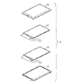
- FIG. 1 showing an embodiment of the present invention, is a diagram showing a schematic configuration of a liquid crystal module.
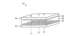
- FIG. 1, showing an embodiment of the present invention is a diagram illustrating a schematic configuration of a first liquid crystal display element.
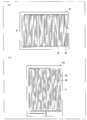
- FIG. It is a figure which shows the board
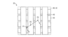
- 1, showing an embodiment of the present invention is a diagram illustrating an electrode arrangement of a first liquid crystal display element.
- FIG. FIG. 5 shows an embodiment of the present invention and is a cross-sectional view taken along line AA of FIG. It is a figure which shows the example of an interference fringe. It is a figure which shows the thickness of a transparent electrode, and the result of visual confirmation.
- the present invention will be described using a liquid crystal module provided with two liquid crystal display elements and capable of three-dimensional display as an example.
- liquid crystal display element of the present invention is used in a set of two sheets, but it can also be used alone.
- FIG. 1 is a diagram showing a schematic configuration of a liquid crystal module 10 of the present embodiment.
- the liquid crystal module 10 includes two liquid crystal display elements, a first liquid crystal display element 20 (liquid crystal display element) and a second liquid crystal display element 30.
- the two liquid crystal display elements enable three-dimensional display (3D display) in the liquid crystal module 10.
- 3D display three-dimensional display
- the liquid crystal module 10 includes a backlight 32, a second liquid crystal display element 30, a first liquid crystal display element 20, and a bezel 34 as main components. And each said component is piled up in said order.
- the second liquid crystal display element 30 functions as an image display element and displays an image.
- the configuration of the second liquid crystal display element 30 is not particularly limited.
- an active matrix type liquid crystal display element in which a TFT element is provided as a switch in each pixel arranged in a matrix type can be provided.
- the first liquid crystal display element 20 functions as a parallax barrier.
- FIG. 2 is a diagram showing a schematic configuration of the first liquid crystal display element 20.
- the first liquid crystal display element 20 of the present embodiment is A liquid crystal layer 60 is sandwiched between a first substrate 42 and a second substrate 44 which are two opposing substrates.
- a surface of the first substrate 42 and the second substrate 44 facing the liquid crystal layer 60 is provided with a first transparent electrode 46 and a second transparent electrode 48, respectively.
- the first transparent electrode 46 and the second transparent electrode 48 are made of ITO and are almost transparent.
- FIG. 3A and 3B are diagrams showing a schematic configuration of the substrate according to the present embodiment, in which FIG. 3A shows the first substrate 42 and FIG. 3B shows the second substrate 44.
- each transparent electrode 46 and the second transparent electrode 48 are both formed in a comb shape.
- each transparent electrode has a plurality of stripe-shaped extending portions by forming a plurality of slits in parallel.
- each transparent electrode is arranged so that two comb teeth facing each other mesh.
- the extending portions of the two comb teeth are arranged one by one.
- the transparent electrode is provided with only the comb-shaped transparent electrode.
- the transparent electrode has a comb-teeth extension direction (extension direction of the extension portion) of each transparent electrode in a plan view in a state where the two substrates are opposed to each other. Are formed so as to be orthogonal to each other.
- the extending directions of the comb teeth differ by 90 degrees in each substrate.
- the first transparent electrode 46 (pixel electrode) provided on the first substrate 42 as the segment side substrate has a comb tooth extending direction parallel to the rectangular short side direction. It is.
- the extending direction of the comb teeth is parallel to the long side direction of the rectangle.
- the extending direction of the comb teeth of the first transparent electrode 46 and the extending direction of the comb teeth of the second transparent electrode 48 are in plan view.
- the first substrate 42 and the second substrate 44 are bonded so as to be orthogonal to each other.
- FIG. 4 shows an embodiment of the present invention and is a diagram showing an electrode arrangement of the first liquid crystal display element 20. Specifically, a schematic configuration of the first transparent electrode 46 and the second transparent electrode 48 when the first liquid crystal display element 20 is viewed in plan from the surface of the second substrate 44 is shown.
- the first liquid crystal display element 20 is configured such that the comb-like electrodes are orthogonal to each other. And there are only one layer of electrodes.
- the second transparent electrode 48 is present, but the first transparent electrode 46 is not present. Therefore, the transparent electrode has only one layer in plan view.
- FIG. 5 is a cross-sectional view taken along the line AA of FIG. 4 and shows a cross-sectional configuration of the first liquid crystal display element 20.
- the transmitted lights L1 to L3 in FIG. 5 indicate transmitted lights at the points P1 to P3 in FIG.
- the transmitted lights L1 to L3 are the same in FIG.
- the optical path lengths in the liquid crystal layer 60 are different at the respective points P1 to P3 (optical path difference). That is, the transmitted light L1 to L3 have different optical path lengths, and the optical path lengths become shorter in the order of the optical path lengths L1, L2, and L3.
- interference fringes When there is an optical path difference at adjacent locations as described above, interference fringes may be observed when the liquid crystal display element is viewed in plan.
- FIG. 6 shows an example of the interference fringes.
- FIG. 6 shows a rainbow-shaped moire as an example of the interference fringes observed when the first liquid crystal display element 20 is viewed in plan.
- the interference fringes are particularly easily observed when the first liquid crystal display element 20 is in a transmissive state.
- the first liquid crystal display element 20 is composed of normally white, it is easily observed when the voltage is turned off.
- FIG. 7 shows the thickness of the transparent electrode and the result of visually confirming the liquid crystal display element.
- the thickness of the first transparent electrode 46 and the second transparent electrode 48 is changed, and the first liquid crystal display element 20 is visually observed (visual confirmation). Results are shown.
- the first transparent electrode 46 and the second transparent electrode 48 have the same thickness.
- the above visual confirmation items are observation of interference fringes (rainbow-shaped moire) in a transmission state (voltage is OFF in normally white) and lighting failure (orientation failure) in a display state (voltage is ON in normally white). It is.
- interference fringes appear when the thickness of the transparent electrode is 70 nm or 100 nm ( ⁇ ), but no interference fringes appear when the thickness of the transparent electrode is 60 nm or less ( ⁇ ). That is, when the thickness of the transparent electrode is reduced, the expression of interference fringes tends to be suppressed, and it is considered that it does not appear at least below 60 nm.
- Lighting failure and transparent electrode thickness On the other hand, lighting failure based on orientation failure tends to occur (x) when the thickness of the transparent electrode is reduced. Specifically, it does not occur when the thickness of the transparent electrode is 35 nm or more ( ⁇ ), whereas when the thickness of the transparent electrode is 20 nm, alignment failure occurs.
- the above alignment failure is considered to be due to the fact that a desired voltage is not applied to the liquid crystal molecules. This tends to occur when the sheet resistance of the transparent electrode is too large.
- the sheet resistance is 100 ⁇ or less. For this reason, it is considered that the above-mentioned orientation failure is unlikely to occur, and thus it is difficult to cause a lighting failure.
- both the first transparent electrode 46 and the second transparent electrode 48 have a thickness of 60 nm or less and 25 nm or more.
- the sheet resistance of the transparent electrode is 100 ⁇ or less.
- the occurrence of interference fringes and lighting failures are suppressed.
- liquid crystal module 10 of this Embodiment is equipped with the 1st liquid crystal display element 20 by which generation
- the liquid crystal module 10 is provided with two liquid crystal display elements (the first liquid crystal display element 20 and the second liquid crystal display element 30), thereby enabling three-dimensional display.
- the first liquid crystal display element 20 of the present embodiment is less likely to generate interference fringes in the transmissive state.
- a desired pattern such as a stripe pattern is displayed on the first liquid crystal display element 20 that functions as a parallax barrier.
- the viewer looks at the image displayed on the second liquid crystal display element 30 through the symbol displayed on the first liquid crystal display element 20.
- the first liquid crystal display element 20 of the present embodiment is less likely to cause display defects in the display state. Specifically, for example, there are few cases where a pattern such as a stripe pattern is interrupted or the contrast is lowered.
- the liquid crystal module 10 of the present embodiment may include a bonding interval adjusting member between the first liquid crystal display element 20 and the second liquid crystal display element 30. Thereby, the bonding interval between the first liquid crystal display element 20 and the second liquid crystal display element 30 can be adjusted.
- the image displayed on the second liquid crystal display element 30 functioning as a pixel display element is not displayed as it is to the viewer, as in the case of performing three-dimensional display. Display through the barrier.
- a desired pattern such as a stripe pattern is displayed on the first liquid crystal display element 20 that functions as a parallax barrier. Furthermore, the space
- the viewer views the image displayed on the second liquid crystal display element 30 through the symbol displayed on the first liquid crystal display element 10.
- the first liquid crystal display element 20 of the present embodiment is less likely to cause display defects in the display state. Specifically, for example, there are few cases where a pattern such as a stripe pattern is interrupted or the contrast is lowered.
- the thickness of the transparent electrode of the first liquid crystal display element 20 of the present embodiment is optimized, a liquid crystal display element with a good display quality in which the occurrence of interference fringes and the like is suppressed It has become.
- the thickness of the liquid crystal layer 60 is not particularly limited.
- the thickness of the liquid crystal layer 60 may be, for example, 4.5 ⁇ m to 7.0 ⁇ m, preferably 4.6 ⁇ m to 6.4 ⁇ m.
- the material of the transparent electrode is not limited to ITO, and other transparent conductive materials can also be used.
- the refractive index of the transparent conductive material is preferably in the range of 1.8 to 2.0.
- the transparent electrode is a double-sided feed type in which the opposing comb teeth are combined, but is not limited to the above configuration.
- both the first transparent electrode and the second transparent electrode are comb-shaped
- the present invention is not limited to this.
- the second transparent electrode 48 is a solid electrode, light scattering at the edge portion of the electrode can be suppressed. Thereby, the expression of interference fringes can be suppressed.
- the first liquid crystal display element 20 can also be used as a single unit.
- the first liquid crystal display element 20 can be used as a simple matrix type STN display element. Even in this case, it is possible to realize a liquid crystal display element in which the occurrence of interference fringes and the occurrence of lighting failures are suppressed.
- the liquid crystal display element of the present invention is At least one of the first transparent electrode and the second transparent electrode can be formed in a comb shape.
- the liquid crystal display element of the present invention is The first transparent electrode and the second transparent electrode are formed in a comb shape, The extending direction of the comb teeth of the first transparent electrode and the extending direction of the comb teeth of the second transparent electrode can be orthogonal to each other in plan view.
- the transparent electrode is comb-shaped. Therefore, there are many places where optical path differences occur, and interference fringes are likely to appear.
- the comb-like transparent electrodes facing each other are orthogonal, interference fringes are more likely to appear.
- the transparent electrode is thin, the occurrence of interference fringes can be suppressed.
- the liquid crystal display element of the present invention is The transparent electrode provided in the display area of the first substrate is only the comb-shaped first transparent electrode, The transparent electrode provided in the display area of the second substrate may be only the comb-shaped second transparent electrode.
- the transparent electrode is thin, it can be suppressed.
- the liquid crystal display element of the present invention is The sheet resistance of the first transparent electrode and the second transparent electrode is preferably 100 ⁇ or less.
- the liquid crystal display element of the present invention is The d1 and d2 are preferably 25 nm or more.
- the sheet resistance of the transparent electrode is 100 ⁇ or less, or the thickness of the transparent electrode is 25 nm or more, it is easy to apply a desired voltage to the liquid crystal layer.
- the liquid crystal display element of the present invention is It can also be used for three-dimensional display.
- the liquid crystal module of the present invention is A liquid crystal module comprising a second liquid crystal display element in addition to the above liquid crystal display element, The liquid crystal display element and the second liquid crystal display element are arranged so as to overlap in a plan view, A three-dimensional display can be performed by displaying a desired design on the liquid crystal display element.
- the liquid crystal display element in which the occurrence of interference fringes is suppressed can be used as, for example, a parallax barrier in three-dimensional display.
- the liquid crystal display element of the present invention suppresses the occurrence of interference fringes, it can be suitably used for a liquid crystal display element having a comb-like transparent electrode.
Landscapes
- Physics & Mathematics (AREA)
- Nonlinear Science (AREA)
- Geometry (AREA)
- Mathematical Physics (AREA)
- Chemical & Material Sciences (AREA)
- Crystallography & Structural Chemistry (AREA)
- General Physics & Mathematics (AREA)
- Optics & Photonics (AREA)
- Liquid Crystal (AREA)
- Devices For Indicating Variable Information By Combining Individual Elements (AREA)
Abstract
Description
第1基板と第2基板とに液晶層が挟持されてなる、液晶表示素子であって、
上記第1基板の表示領域には第1透明電極が設けられており、
上記第2基板の表示領域には第2透明電極が設けられており、
上記第1透明電極の厚さをd1とし、上記第2透明電極の厚さをd2とした場合、
上記d1及びd2のうちの、少なくとも何れか一方が60nm以下であることを特徴とする。
上記図1に示すように、上記液晶モジュール10は、主な構成部品として、バックライト32、第2液晶表示素子30、第1液晶表示素子20、及び、ベゼル34を備えている。そして、上記各構成部品は、上記の順に重ね合わされている。
上記第2液晶表示素子30は、画像表示素子として機能するものであり、画像が表示される。
上記第1液晶表示素子20は、視差バリアとして機能するものである。
対向する2枚の基板である第1基板42と第2基板44とに、液晶層60が挟まれた構造を有している。
つぎに、上記各透明電極の形状について説明する。図3は、本実施の形態の基板の概略構成を示す図であり、(a)は第1基板42を示し、(b)は第2基板44を示している。
また、上記透明電極は、上記図2にも示すように、2枚の基板が対向配置された状態で、平面視において、各々の透明電極の櫛歯の延伸方向(上記延伸部分の延伸方向)が直交するように形成されている。
上記のように、本実施の形態の第1液晶表示素子20では、上記第1透明電極46の櫛歯の延伸方向と、上記第2透明電極48の櫛歯の延伸方向とが、平面視において直交するように、第1基板42と第2基板44とが貼り合わされている。
図5は、上記図4のA-A線断面図であり、上記第1液晶表示素子20の断面構成を示している。
上記のように隣接する箇所で光路差が存在する場合、その液晶表示素子を平面視した際、干渉縞が観察される場合がある。
上記干渉縞の発現に関し、本実施の形態の第1液晶表示素子20では、透明電極の厚さが最適化されているため、その発現が抑制されている。
図7に示す例では、第1透明電極46及び第2透明電極48の厚さを20nm~100nmの間で変化させて、視認確認を行っている。
一方、配向不良に基づく点灯不良は、透明電極の厚さが薄くなると発生する(×)傾向にある。具体的には、透明電極の厚さが35nm以上であると発生しない(○)のに対して、透明電極の厚さが20nmでは、配向不良が発生する。
本実施の形態の第1液晶表示素子20では、第1透明電極46及び第2透明電極48が共に、その厚さが60nm以下25nm以上となっている。そして、上記透明電極のシート抵抗は100Ω以下となっている。
そして、本実施の形態の液晶モジュール10は、干渉縞及び点灯不良の発生が抑制された第1液晶表示素子20が備えられているため、良好な表示を行うことができる。
まず、二次元の表示について説明する。二次元の表示を行う際は、
画像表示素子として機能する第2液晶表示素子30に表示された画像をそのまま観者に対して表示する。そのため、視差バリアとして機能する第1液晶表示素子20は、透過状態となっている。
つぎに、三次元の表示について説明する。三次元の表示を行う際は、画像表示素子として機能する第2液晶表示素子30に表示された画像をそのまま観者に対して表示するのではなく、視差バリアを介して表示する。
さらに、マルチビュー表示について説明する。本実施の形態の液晶モジュール10は、第1液晶表示素子20と第2液晶表示素子30との間に、貼合間隔調整部材を備えていてもよい。これにより、上記第1液晶表示素子20と上記第2液晶表示素子30との貼り合せ間隔を調整することができる。
上記第1透明電極及び上記第2透明電極のうち、少なくとも何れか一方を、櫛歯状に形成することができる。
上記第1透明電極及び上記第2透明電極は、櫛歯状に形成されており、
上記第1透明電極の櫛歯の延伸方向と、上記第2透明電極の櫛歯の延伸方向とを、平面視において直交させることができる。
上記第1基板の表示領域に設けられている透明電極は、櫛歯状の上記第1透明電極のみであり、
上記第2基板の表示領域に設けられている透明電極は、櫛歯状の上記第2透明電極のみとすることができる。
上記第1透明電極及び上記第2透明電極のシート抵抗を100Ω以下とすることが好ましい。
上記d1及びd2が25nm以上であることが好ましい。
三次元表示に用いることもできる。
上記の液晶表示素子に加えて、第2液晶表示素子が備えられてなる液晶モジュールであって、
上記液晶表示素子と上記第2液晶表示素子とは、平面視において重なるように配置されており、
上記液晶表示素子に所望の図柄が表示されることで三次元表示が行われるようにすることができる。
20 第1液晶表示素子
30 第2液晶表示素子
32 バックライト
34 ベゼル
42 第1基板 (セグメント側基板)
44 第2基板 (コモン側基板)
46 第1透明電極 (画素電極)
48 第2透明電極 (対向電極)
60 液晶層
D 表示領域
P1~P3 地点
L1~L3 透過光
Claims (8)
- 第1基板と第2基板とに液晶層が挟持されてなる、液晶表示素子であって、
上記第1基板の表示領域には第1透明電極が設けられており、
上記第2基板の表示領域には第2透明電極が設けられており、
上記第1透明電極の厚さをd1とし、上記第2透明電極の厚さをd2とした場合、
上記d1及びd2のうちの、少なくとも何れか一方が60nm以下であることを特徴とする液晶表示素子。 - 上記第1透明電極及び上記第2透明電極のうち、少なくとも何れか一方は、櫛歯状に形成されていることを特徴とする請求項1に記載の液晶表示素子。
- 上記第1透明電極及び上記第2透明電極は、櫛歯状に形成されており、
上記第1透明電極の櫛歯の延伸方向と、上記第2透明電極の櫛歯の延伸方向とが、平面視において直交していることを特徴とする請求項1に記載の液晶表示素子。 - 上記第1基板の表示領域に設けられている透明電極は、櫛歯状の上記第1透明電極のみであり、
上記第2基板の表示領域に設けられている透明電極は、櫛歯状の上記第2透明電極のみであることを特徴とする請求項1又は3に記載の液晶表示素子。 - 上記第1透明電極及び上記第2透明電極のシート抵抗が100Ω以下であることを特徴とする請求項1から4の何れか1項に記載の液晶表示素子。
- 上記d1及びd2が25nm以上であることを特徴とする請求項1から5の何れか1項に記載の液晶表示素子。
- 三次元表示に用いられることを特徴とする請求項1から6の何れか1項に記載の液晶表示素子。
- 請求項1から7の何れか1項に記載の液晶表示素子に加えて、第2液晶表示素子が備えられてなる液晶モジュールであって、
上記液晶表示素子と上記第2液晶表示素子とは、平面視において重なるように配置されており、
上記液晶表示素子に所望の図柄が表示されることで三次元表示が行われることを特徴とする液晶モジュール。
Priority Applications (3)
| Application Number | Priority Date | Filing Date | Title |
|---|---|---|---|
| AU2011337858A AU2011337858B2 (en) | 2010-11-30 | 2011-11-24 | Liquid crystal display element and liquid crystal module |
| SG2013030101A SG189485A1 (en) | 2010-11-30 | 2011-11-24 | Liquid crystal display element and liquid crystal module |
| US13/879,222 US9041873B2 (en) | 2010-11-30 | 2011-11-24 | Liquid crystal display element and liquid crystal module |
Applications Claiming Priority (2)
| Application Number | Priority Date | Filing Date | Title |
|---|---|---|---|
| JP2010-267518 | 2010-11-30 | ||
| JP2010267518 | 2010-11-30 |
Publications (1)
| Publication Number | Publication Date |
|---|---|
| WO2012073793A1 true WO2012073793A1 (ja) | 2012-06-07 |
Family
ID=46171734
Family Applications (1)
| Application Number | Title | Priority Date | Filing Date |
|---|---|---|---|
| PCT/JP2011/077099 Ceased WO2012073793A1 (ja) | 2010-11-30 | 2011-11-24 | 液晶表示素子及び液晶モジュール |
Country Status (4)
| Country | Link |
|---|---|
| US (1) | US9041873B2 (ja) |
| AU (1) | AU2011337858B2 (ja) |
| SG (1) | SG189485A1 (ja) |
| WO (1) | WO2012073793A1 (ja) |
Families Citing this family (3)
| Publication number | Priority date | Publication date | Assignee | Title |
|---|---|---|---|---|
| CN110911440B (zh) * | 2018-09-14 | 2020-10-16 | 云谷(固安)科技有限公司 | 显示面板、显示屏和显示终端 |
| WO2020052232A1 (zh) * | 2018-09-14 | 2020-03-19 | 昆山国显光电有限公司 | 显示面板、显示屏和显示终端 |
| CN110911439B (zh) * | 2018-09-14 | 2023-08-18 | 云谷(固安)科技有限公司 | 显示面板、显示屏和显示终端 |
Citations (3)
| Publication number | Priority date | Publication date | Assignee | Title |
|---|---|---|---|---|
| JPH0876146A (ja) * | 1994-06-29 | 1996-03-22 | Toshiba Corp | 液晶表示装置 |
| JP2007248674A (ja) * | 2006-03-15 | 2007-09-27 | Ricoh Co Ltd | 光学素子と光偏向素子及び画像表示装置 |
| JP2010224191A (ja) * | 2009-03-23 | 2010-10-07 | Toshiba Corp | 立体画像表示装置 |
Family Cites Families (4)
| Publication number | Priority date | Publication date | Assignee | Title |
|---|---|---|---|---|
| JP3529434B2 (ja) | 1993-07-27 | 2004-05-24 | 株式会社東芝 | 液晶表示素子 |
| US5434690A (en) | 1993-07-27 | 1995-07-18 | Kabushiki Kaisha Toshiba | Liquid crystal device with pixel electrodes in an opposed striped form |
| US8493440B2 (en) * | 2005-12-20 | 2013-07-23 | Koninklijke Philips N.V. | Autostereoscopic display device |
| US8164727B2 (en) * | 2009-11-30 | 2012-04-24 | Rensselaer Polytechnic Institute | Liquid crystal display with refractive index matched electrodes |
-
2011
- 2011-11-24 AU AU2011337858A patent/AU2011337858B2/en not_active Ceased
- 2011-11-24 SG SG2013030101A patent/SG189485A1/en unknown
- 2011-11-24 WO PCT/JP2011/077099 patent/WO2012073793A1/ja not_active Ceased
- 2011-11-24 US US13/879,222 patent/US9041873B2/en not_active Expired - Fee Related
Patent Citations (3)
| Publication number | Priority date | Publication date | Assignee | Title |
|---|---|---|---|---|
| JPH0876146A (ja) * | 1994-06-29 | 1996-03-22 | Toshiba Corp | 液晶表示装置 |
| JP2007248674A (ja) * | 2006-03-15 | 2007-09-27 | Ricoh Co Ltd | 光学素子と光偏向素子及び画像表示装置 |
| JP2010224191A (ja) * | 2009-03-23 | 2010-10-07 | Toshiba Corp | 立体画像表示装置 |
Also Published As
| Publication number | Publication date |
|---|---|
| US20130215371A1 (en) | 2013-08-22 |
| US9041873B2 (en) | 2015-05-26 |
| AU2011337858B2 (en) | 2014-05-15 |
| AU2011337858A1 (en) | 2013-05-02 |
| SG189485A1 (en) | 2013-05-31 |
Similar Documents
| Publication | Publication Date | Title |
|---|---|---|
| JP6180543B2 (ja) | 表示装置 | |
| TW201239468A (en) | Display device | |
| CN103154801B (zh) | 显示装置 | |
| JP2015045665A (ja) | 立体表示装置 | |
| JP3701661B2 (ja) | 表示パネルおよび表示装置 | |
| JP6223158B2 (ja) | 液晶表示装置 | |
| US7602466B2 (en) | 2-dimensional and 3-dimensional image display device and method of manufacturing the same | |
| JP6230696B2 (ja) | タッチパネル付き表示装置 | |
| WO2013080927A1 (ja) | 立体表示装置 | |
| JP2011169949A (ja) | 3次元画像表示装置 | |
| JP6125027B2 (ja) | 立体表示装置 | |
| WO2012073793A1 (ja) | 液晶表示素子及び液晶モジュール | |
| KR101580362B1 (ko) | 시차 장벽 및 디스플레이 장치 | |
| CN101419340A (zh) | 可切换式光栅及平面显示器 | |
| JP2019095544A (ja) | 画像表示装置 | |
| JPWO2012014827A1 (ja) | スイッチ液晶パネル及び表示装置 | |
| CN105759436B (zh) | 裸眼三维显示系统和折射率调节装置 | |
| CN103733125A (zh) | 立体显示装置 | |
| TW202141125A (zh) | 電光面板、屏障快門面板、顯示裝置及顯示面板 | |
| JP2006039226A (ja) | パララックスバリア素子およびそれを備えた表示装置 | |
| JP2007121702A (ja) | 液晶表示パネル | |
| JP2014132347A (ja) | 液晶パララックスバリア、表示装置及び液晶表示装置 | |
| JP2009133938A (ja) | 液晶表示装置 | |
| JP2013114114A (ja) | 液晶表示素子及びその生産方法 |
Legal Events
| Date | Code | Title | Description |
|---|---|---|---|
| 121 | Ep: the epo has been informed by wipo that ep was designated in this application |
Ref document number: 11845190 Country of ref document: EP Kind code of ref document: A1 |
|
| WWE | Wipo information: entry into national phase |
Ref document number: 13879222 Country of ref document: US |
|
| ENP | Entry into the national phase |
Ref document number: 2011337858 Country of ref document: AU Date of ref document: 20111124 Kind code of ref document: A |
|
| NENP | Non-entry into the national phase |
Ref country code: DE |
|
| 122 | Ep: pct application non-entry in european phase |
Ref document number: 11845190 Country of ref document: EP Kind code of ref document: A1 |
|
| NENP | Non-entry into the national phase |
Ref country code: JP |