WO2012067446A2 - 고분자 표면보호막을 가진 반도체 나노입자 및 이의 제조방법 - Google Patents
고분자 표면보호막을 가진 반도체 나노입자 및 이의 제조방법 Download PDFInfo
- Publication number
- WO2012067446A2 WO2012067446A2 PCT/KR2011/008804 KR2011008804W WO2012067446A2 WO 2012067446 A2 WO2012067446 A2 WO 2012067446A2 KR 2011008804 W KR2011008804 W KR 2011008804W WO 2012067446 A2 WO2012067446 A2 WO 2012067446A2
- Authority
- WO
- WIPO (PCT)
- Prior art keywords
- group
- protective film
- surface protective
- polymer surface
- polymer
- Prior art date
- Legal status (The legal status is an assumption and is not a legal conclusion. Google has not performed a legal analysis and makes no representation as to the accuracy of the status listed.)
- Ceased
Links
Images
Classifications
-
- B—PERFORMING OPERATIONS; TRANSPORTING
- B82—NANOTECHNOLOGY
- B82Y—SPECIFIC USES OR APPLICATIONS OF NANOSTRUCTURES; MEASUREMENT OR ANALYSIS OF NANOSTRUCTURES; MANUFACTURE OR TREATMENT OF NANOSTRUCTURES
- B82Y30/00—Nanotechnology for materials or surface science, e.g. nanocomposites
-
- B—PERFORMING OPERATIONS; TRANSPORTING
- B82—NANOTECHNOLOGY
- B82Y—SPECIFIC USES OR APPLICATIONS OF NANOSTRUCTURES; MEASUREMENT OR ANALYSIS OF NANOSTRUCTURES; MANUFACTURE OR TREATMENT OF NANOSTRUCTURES
- B82Y40/00—Manufacture or treatment of nanostructures
-
- H—ELECTRICITY
- H10—SEMICONDUCTOR DEVICES; ELECTRIC SOLID-STATE DEVICES NOT OTHERWISE PROVIDED FOR
- H10P—GENERIC PROCESSES OR APPARATUS FOR THE MANUFACTURE OR TREATMENT OF DEVICES COVERED BY CLASS H10
- H10P14/00—Formation of materials, e.g. in the shape of layers or pillars
- H10P14/20—Formation of materials, e.g. in the shape of layers or pillars of semiconductor materials
- H10P14/34—Deposited materials, e.g. layers
- H10P14/3402—Deposited materials, e.g. layers characterised by the chemical composition
- H10P14/3404—Deposited materials, e.g. layers characterised by the chemical composition being Group IVA materials
- H10P14/3411—Silicon, silicon germanium or germanium
-
- H—ELECTRICITY
- H10—SEMICONDUCTOR DEVICES; ELECTRIC SOLID-STATE DEVICES NOT OTHERWISE PROVIDED FOR
- H10P—GENERIC PROCESSES OR APPARATUS FOR THE MANUFACTURE OR TREATMENT OF DEVICES COVERED BY CLASS H10
- H10P14/00—Formation of materials, e.g. in the shape of layers or pillars
- H10P14/20—Formation of materials, e.g. in the shape of layers or pillars of semiconductor materials
- H10P14/34—Deposited materials, e.g. layers
- H10P14/3451—Structure
- H10P14/3452—Microstructure
- H10P14/3461—Nanoparticles
Definitions
- the present invention relates to a semiconductor nanoparticle having a polymer surface protective film and a method for manufacturing the same, and more particularly, to a method for manufacturing a group 4 semiconductor nanoparticle having a size distribution of several tens of nanometers and a polymer surface protective film formed on a surface thereof. It relates to a Group 4 semiconductor nanoparticles prepared according to.
- Semiconductor nanoparticles are called semiconductor nanocrystals, semiconductor nanopowders, etc., and are commonly known as quantum dots.
- Semiconductor materials such as silicon and germanium, are known to have no opto-electric or electro-optic or electroluminescent properties in the state of a typical visible, bulk scale single crystal structure.
- the structure is very small, and if it is made in nano scale, the energy band gap of the material is expanded by quantum confinement effects, thereby changing the electrical and optical properties, and the visible light region. It is known that luminescence at can be achieved.
- it is usually necessary to form a particle state separated from the main body in a bulk state or protrude from the main body to have a very large ratio of volume to surface area.
- Semiconductor nanoparticles are crystalline semiconductor materials made of inorganic compounds, and have unique photophysical, photochemical, and nonlinear optical properties due to quantum size effects, and thus have potential applications in various fields such as medical applications, photocatalysts, charge transfer devices, and analytical chemistry. Attention is focused because of sex.
- An object of the present invention is to form a polymer surface protective film on the surface to prevent the surface is oxidized, a method for manufacturing a semiconductor nanoparticles that can be produced to have a variety of size distribution of several tens of nanoscales and a semiconductor manufactured using To provide nanoparticles.
- step 1 Adding a dispersant to the solvent and stirring to prepare a dispersant solution (step 1);
- It provides a method for producing a semiconductor nanoparticle having a polymer surface protective film comprising a step (step 3) to prepare a mixture by adding a reducing agent to the stirred mixed solution in step 2 by stirring.
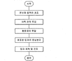
- FIG. 1 schematically illustrates a manufacturing process of semiconductor nanoparticles according to the present invention.
- a dispersant is added to a vessel containing a solvent and stirred to prepare a dispersant solution (step 1).
- a solvent may be used, but is not limited thereto.
- Various solvents such as ethylene glycol can be used.
- the dispersant for example, polyvinylpyrrolidone, polyacrylic acid hydrazide, poly-N-vinyl-5-methoxazolidon , N-alkyl polyimine, polyvinylalcohol, N-acetyl polyimine, polyacrylamide, poly-L-lysine hydrobromide (poly-L -lysinhydrobromide, polyacroleine, benzyl-dodecyl-dimethylammonium chloride, polyacrylic acid, polyethylenimine, 4-vinylpyridine And a composite polymer consisting of a polymer selected from the group consisting of methylvinyl ketone (methylvinylketone) or oligomers thereof.
- a repeating type of hydrocarbon molecule in which a single molecule or oligomer unit is covalently linked to the compound molecular weight of 10,000mole / g or more and complex polymers capable of forming a mixed ionic covalent bond with a group 4 element It can be used as a dispersant.
- a Group 4 element-containing salt is added to the prepared dispersant solution and stirred to prepare a mixed solution (step 2).
- the Group 4 element-containing salt is used as a precursor material for producing Group 4 semiconductor nanoparticles, for example, may be used a silicon salt or germanium salt.
- a salt containing one kind selected from the group consisting of Group I elements, Group II elements, Group III elements, Group V elements, and Group VI elements together with Group 4 element-containing salts Or two or more mixed salts may be further added.
- a salt or a mixed salt containing one or more selected from the group consisting of Group I elements, Group II elements, Group III elements, Group V elements and Group VI elements is further added.
- the resistance, conductivity, charge mobility, magnetic properties, etc. of the semiconductor nanoparticles finally manufactured by the doping effect can be controlled.
- the salt containing at least one selected from the group consisting of Group I elements, Group II elements, Group III elements, Group V elements, and Group VI elements may be selected from 0 to about 100 parts by weight of the Group 4 element-containing salt. It is preferably included in 30 parts by weight.
- step 3 a reducing agent is added to the mixed solution stirred in step 2 to stir to prepare a mixture (step 3).
- the reducing agent may be sodium naphthalide, lithium naphthalide, potassium naphthalide and hydrides, or metals of group 1, and the hydrides may be, for example, lithium aluminum hydride (LiAlH 4 ).
- the hydrides may be, for example, lithium aluminum hydride (LiAlH 4 ).
- Sodium borohydride, aluminum hydride (AlH 3 ), lithium hydride, sodium hydride (NaH), potassium hydride and the like can be used, for example, group 1 metals such as lithium or sodium Can be used.
- the weight ratio of the Group 4 element-containing salt, dispersant, and reducing agent used in the above Steps 1 to 3 is preferably 0.1 to 15.0: 0.5 to 50.0: 0.5 to 100, respectively.
- the mixture prepared in step 3 is separated by centrifugation several times, dried using a vacuum dryer, and collected in powder form to obtain final semiconductor nanoparticles. can do.
- the present invention also provides a semiconductor nanoparticle comprising a Group 4 semiconductor nanoparticle and a polymer surface protective film attached to the Group 4 semiconductor nanoparticle.
- the semiconductor nanoparticles may be prepared in a size of about 5 nanometers to 500 nanometers according to the method of manufacturing the semiconductor nanoparticles of the present invention described above.
- the semiconductor nanoparticles prepared as described above have the advantage that they can be dispersed in the aqueous system (H 2 O) by the dispersion effect of the surface protection film of the polymer.
- the present invention can prevent the surface oxidation by forming a polymer surface protective film, can provide a method for manufacturing semiconductor nanoparticles having various size distribution of several tens of nanometers, and also the resistance, conductivity, charge of semiconductor nanoparticles It is possible to provide a method for manufacturing semiconductor nanoparticles that can control mobility and magnetic properties.
- FIG. 1 is a flow chart schematically showing a manufacturing process of a semiconductor nanoparticle according to the present invention.
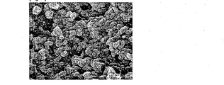
- Example 2 is a scanning electron microscope (SEM) photograph of the semiconductor nanoparticles prepared in Example 1 according to the present invention.
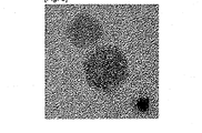
- Figure 3 is a scanning transmission micrograph of the semiconductor nanoparticles prepared in Example 1 according to the present invention.
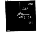
- Figure 4 is a local electron refraction photo of the scanning transmission microscope of the semiconductor nanoparticles prepared in Example 1 according to the present invention.
- Dispersant is polyvinylpyrrolidone (PVP) in a mixture of 1.11g of glyme (glyme) dissolved in 10mL solvent through the rotation for more than 10 minutes stirring at room temperature and here a silicon tetra-chloride salt in a silicon (Silicon tetra chloride, SiCl 4 ) was sufficiently stirred with a 10 mmol syringe and slowly added. Thereafter, 40 mmol of sodium napthalide as a reducing agent was added thereto, followed by stirring to prepare a mixture. After maintaining the mixture for 2 hours, the reaction was completed and the prepared particles were separated using a centrifuge.
- PVP polyvinylpyrrolidone
- the separated particles were purified through centrifuge five times using ultrapure water and the particles prepared in a vacuum dryer were collected in powder form to obtain semiconductor nanoparticles. SEM photographs of the prepared semiconductor nanoparticles were taken. 2, the transmission microscope picture was taken in FIG. 3, and the transmission microscope local electron refraction picture was taken in FIG.
- Dispersant is polyvinylpyrrolidone (PVP) in a mixture of 1.11g of glyme (glyme) dissolved in 10mL solvent through the rotation for more than 10 minutes stirring at room temperature and here a silicon tetra-chloride salt in a silicon (Silicon tetra chloride, SiCl 4 ) was added 10 mmol, and 1 mmol of phosphorus salt (PCl 3 ) or boron salt (BCl 3 ) was added slowly using a syringe, respectively, and stirred sufficiently. 40 mmol of sodium napthalide as a reducing agent was added thereto, followed by stirring to prepare a mixture.
- PVP polyvinylpyrrolidone
- the reaction was completed and the prepared particles were separated using a centrifuge.
- the separated particles were purified using ultrapure water through a centrifuge five times, and the particles prepared using a vacuum dryer were collected in powder form to obtain semiconductor nanoparticles.
- the semiconductor nanoparticles prepared in Example 1 according to the present invention is formed of nanoparticles of several nanometers to several tens of nanometers in size.
- the diffraction in the ⁇ 111 ⁇ and ⁇ 220 ⁇ plane gratings shows lattice interlayer distances of 3.13 ⁇ and 1.92 ,, and the two interlayer gaps represent typical interlayer distances of the silicon nanoparticle lattice. Therefore, it can be confirmed that the synthesized nanoparticles are silicon.
- a polymer surface protective film is formed on the surface to prevent the surface from being oxidized, and semiconductor nanoparticles having various size distributions of several tens of nanometers can be manufactured.
Landscapes
- Engineering & Computer Science (AREA)
- Chemical & Material Sciences (AREA)
- Nanotechnology (AREA)
- Physics & Mathematics (AREA)
- Condensed Matter Physics & Semiconductors (AREA)
- General Physics & Mathematics (AREA)
- Crystallography & Structural Chemistry (AREA)
- Manufacturing & Machinery (AREA)
- Composite Materials (AREA)
- Materials Engineering (AREA)
- Processes Of Treating Macromolecular Substances (AREA)
- Formation Of Insulating Films (AREA)
Abstract
본 발명은 수십 나노미터의 다양한 크기 분포를 가지며 표면에 고분자 표면보호막이 형성된 4족 반도체 나노입자를 제조하는 방법 및 이에 따라 제조된 4족 반도체 나노입자에 관한 것이다. 본 발명에 따른 반도체 나노입자의 제조방법을 사용하는 경우 고분자 표면보호막이 형성되어 표면이 산화되는 것을 방지할 수 있으며, 수십 나노크기의 다양한 크기 분포를 가진 반도체 나노입자를 제조할 수 있으며, 또한 반도체 나노입자의 저항, 전도도, 전하이동도 및 자기적 성질을 조절할 수 있다.
Description
본 발명은 고분자 표면보호막을 가진 반도체 나노입자 및 이의 제조방법에 관한 것으로, 보다 상세하게는 수십 나노미터의 다양한 크기 분포를 가지며 표면에 고분자 표면보호막이 형성된 4족 반도체 나노입자를 제조하는 방법 및 이에 따라 제조된 4족 반도체 나노입자에 관한 것이다.
반도체 나노입자는 반도체 나노결정, 반도체 나노분말 등으로 명명되며, 보통 양자점(quantum dot)으로 알려져 있다. 반도체 재질인 실리콘이나 게르마늄 등은 통상의 가시적, 대단위(bulk scale) 크기의 단결정 구조체 상태에서 광전(opto-electric) 혹은 전광(electro-optic) 특성이나 전계발광 특성을 갖지 않는 것으로 알려져 있다.
한편, 실리콘, 게르마늄 등에서는 그 구조체 크기가 매우 작아져 나노 스케일(nano scale)로 이루어지면 양자구속 현상(quantum confinement effects)에 의해 물질의 에너지 밴드 갭이 확장되면서 전기적 광학적 특성이 변화되고 가시광선 영역에서의 발광이 이루어질 수 있게 된다고 알려져 있다. 이때, 나노 구조체를 이루기 위해서는 통상 벌크 상태의 본체와 분리되어 입자 상태를 이루거나 본체부에서 돌출되어 매우 큰 부피대 표면적비(ratio of volume to surface area)를 가지도록 형성되는 것이 필요하다.
반도체 나노입자는 무기화합물로 이루어진 결정성 반도체 재료로서, 양자크기효과로 인한 독특한 광물리적, 광화학적, 비선형광학성질을 가지므로, 의료용이나 광촉매, 전하전달 디바이스, 분석화학 등 다양한 분야에서 그 잠재적 응용성 때문에 관심이 집중되고 있다.
그러나, 현재까지 알려진 반도체 나노입자의 제조방법들은 폭발 등으로 인한 안전 문제와 공정이 복잡하고 수율이 떨어지는 등의 문제로 인해 실용화를 위하서는 많은 개선이 필요한 실정이다.
이러한 반도체 나노입자를 제조하기 위한 종래기술로서, Richard K. Baldwin, Katherine A. Pettigrew, Eva Ratai, Matthew P. Augustine and Susan M. Kauzlarich, Chem. Comm., 2002, 1822-1823에서 아래 반응식 1과 같은 공정을 통해 저분자 유기물이 부착된 실리콘 나노입자를 제조하는 방법을 개시한 바 있다.
[반응식 1]
[규칙 제91조에 의한 정정 03.01.2012]

또한, Jamie H. Warner, Akiyoshi Hoshino, Kenji Yamamoto, and Richard. D. Tilley, Angewandte Chemie, Int., 2005, 44, 4550-4554에서는 아래 반응식 2와 같은 공정을 통해 저분자 유기물이 부착된 실리콘 나노입자를 개시하고 있다.
[반응식 2]
[규칙 제91조에 의한 정정 03.01.2012]

상기 반응식 1 및 반응식 2로 표시되는 반도체 나노입자의 제조방법에서는 저분자 유기물을 실리콘 나노입자에 부착시킴으로써 표면이 산화되는 것을 최소화할 수 있는 방법을 개시하고 있다. 그러나 이러한 종래 기술로는 수 나노크기의 반도체 나노입자를 제조하는 데 적합하지만 수십 나노크기의 다양한 크기 분포를 갖는 반도체 나노입자를 제조하는 데 적합하지 않은 문제점이 있다.
본 발명의 목적은 표면에 고분자 표면보호막이 형성되어 표면이 산화되는 것을 방지할 수 있으며, 수십 나노크기의 다양한 크기 분포를 가지도록 제조할 수 있는 반도체 나노입자의 제조방법 및 이를 이용하여 제조된 반도체 나노입자를 제공하는 데 있다.
상기 목적을 달성하기 위하여, 본 발명은,
용매에 분산제를 첨가하고 교반하여 분산제 용액을 제조하는 단계(단계 1);
상기 분산제 용액에 4족 원소함유염을 첨가하고 교반하여 혼합용액을 제조하는 단계(단계 2); 및
상기 단계 2에서 교반된 혼합용액에 환원제를 첨가하여 교반하여 혼합물을 제조하는 단계(단계 3)를 포함하는 고분자 표면보호막을 가진 반도체 나노입자의 제조방법을 제공한다.
이하 본 발명에 따른 반도체 나노입자의 제조공정을 개략적으로 나타낸 도 1을 참조하여 반도체 나노입자의 제조방법을 상세히 설명한다.
우선, 용매가 들어있는 용기에 분산제를 첨가하고 교반하여 분산제 용액을 제조한다(단계 1).
본 발명에서 용매로는 글라임계 용매를 사용할 수 있으나, 이에 제한되는 것은 아니며, 톨루엔, 아니솔 및 테트라하이드로푸란, 사이크로벤젠, 다이글라임,트리글라임,에틸렌글리콘,다이에틸렌글리콜,트리에틸렌글리콜 등의 다양한 용매가 사용될 수 있다.
상기 분산제로는 예를 들어 폴리비닐피롤리돈(polyvinylpyrrolidone), 폴리아크릴산 하이드라지드(polyacrylic acid hydrazide), 폴리-N-비닐-5-메톡사졸리돈(poly-N-vinyl-5-methoxazolidon), N-알킬 폴리이민(N-alkyl polyimine), 폴리비닐알코올(polyvinylalcohol), N-아세틸 폴리이민(N-acetyl polyimine), 폴리아크릴아미드(polyacrylamide), 폴리-L-리신하이드로브로마이드(poly-L-lysinhydrobromide), 폴리아크로레인(polyacroleine), 벤질-도데실-디메틸암모늄 클로라이드(benzyl-dodecyl-dimethylammonium chloride), 폴리아크릴산(polyacrylic acid), 폴리에틸렌이민(polyethylenimine), 4-비닐피리딘(4-vinylpyridine) 및 메틸비닐케톤(methylvinylketone)으로 이루어진 군으로부터 선택된 고분자 또는 이들의 올리고머로 이루어진 복합고분자를 사용될 수 있다. 또한, 단분자 또는 올리고머단위가 공유결합으로 연결되어있는 반복된 형태의 탄화수소분자로서 분자량이 10,000mole/g 이상이며 4족원소와 혼합형 이온성 공유결합(mixed ionic covalent bond) 형성이 가능한 복합고분자들이 분산제로서 사용될 수 있다.
다음으로, 상기 제조된 분산제 용액에 4족 원소함유염을 첨가하고 교반하여 혼합용액을 제조한다(단계 2).
본 발명에서 상기 4족 원소함유염으로는 4족 반도체 나노입자를 제조하기 위한 전구체 물질을 사용하며, 예를 들어, 실리콘염 또는 게르마늄염을 사용할 수 있다.
본 발명의 일 실시형태에 있어서, 상기 단계 2에서는 4족 원소함유염과 함께 I족 원소, II족 원소, III족 원소, V족 원소 및 VI족 원소로 이루어진 군으로부터 선택된 1종을 포함하는 염 또는 2종 이상의 혼합염을 더 첨가할 수 있다.
이와 같이 본 발명에서는 4족 원소함유염과 함께 I족 원소, II족 원소, III족 원소, V족 원소 및 VI족 원소로 이루어진 군으로부터 선택된 1종을 포함하는 염 또는 2종 이상의 혼합염을 더 첨가함으로써 도핑(doping) 효과에 의해 최종적으로 제조되는 반도체 나노입자의 저항, 전도도, 전하이동도, 자기적 성질 등을 조절할 수 있다.
예를 들어, 상기 단계 2에서 4족 원소함유염과 함께 III족 원소인 붕소(boron)가 함유된 염(BCl3)을 첨가하는 경우 p-타입 성질을 갖는 반도체 나노입자를 제조할 수 있으며, V족 원소인 인(phosphorus)을 포함하는 염(PCl3)을 첨가하는 경우 n-타입 성질을 갖는 반도체 나노입자를 제조할 수 있다.
상기 I족 원소, II족 원소, III족 원소, V족 원소 및 VI족 원소로 이루어진 군으로부터 선택된 1종을 포함하는 염 또는 2종 이상의 혼합염은 4족 원소함유염 100 중량부 기준으로 0 ~ 30 중량부로 포함되는 것이 바람직하다.
다음으로, 상기 단계 2에서 교반된 혼합용액에 환원제를 첨가하여 교반하여 혼합물을 제조한다(단계 3).
상기 환원제는 소듐나프탈라이드, 리티움나프탈라이드, 포타슘나프탈라이드와 하이드라이드류, 또는 1족의 금속류가 사용될 수 있으며, 하이드라이드류로는 예를 들어 리티움알루미늄하이드라이드 (LiAlH4), 소디움보로하이드라이드, 알루미늄하이드라인드(AlH3), 리티움하이드라이드, 소디움하이드라이드(NaH), 포타슘하이드라이드 등이 사용될 수 있고, 1족 금속류로는 예를 들어 리튬 또는 소디움 등이 사용될 수 있다.
상기 단계 1 내지 단계 3에서 사용하는 4족 원소함유염, 분산제, 환원제의 중량비는 각각 0.1~15.0 : 0.5~50.0 : 0.5~ 100 으로 사용하는 것이 바람직하다.
본 발명에 따른 반도체 나노입자의 제조방법에서는 상기 단계 3에서 제조된 혼합물은 수회에 걸쳐 원심분리기를 이용하여 분리하고, 진공 건조기 등을 사용하여 건조시켜 분말형태로 포집함으로써 최종적인 반도체 나노입자를 수득할 수 있다.
또한 본 발명은 4족 반도체 나노입자 및 상기 4족 반도체 나노입자에 부착된 고분자 표면보호막을 포함하는 반도체 나노입자를 제공한다.
상기 반도체 나노입자는 상술한 본 발명의 반도체 나노입자의 제조방법에 따라 약 5 나노미터 내지 500 나노미터의 크기로 제조될 수 있다. 아울러, 위와 같이 제조된 반도체 나노입자는 고분자 표면보호막의 분산효과에 의해 수계(H2O)에서 분산이 가능한 장점이 있다.
본 발명은 고분자 표면보호막이 형성되어 표면이 산화되는 것을 방지할 수 있으며, 수십 나노크기의 다양한 크기 분포를 가진 반도체 나노입자의 제조방법을 제공할 수 있으며, 또한 반도체 나노입자의 저항, 전도도, 전하이동도 및 자기적 성질을 조절할 수 있는 반도체 나노입자의 제조방법을 제공할 수 있다.
도 1은 본 발명에 따른 반도체 나노입자의 제조과정을 개략적으로 나타낸 흐름도이다.
도 2는 본 발명에 따라 실시예 1에서 제조된 반도체 나노입자의 주사전자현미경(SEM) 사진이다.
도 3은 본 발명에 따라 실시예 1에서 제조된 반도체 나노입자의 주사투과현미경 사진이다.
도 4는 본 발명에 따라 실시예 1에서 제조된 반도체 나노입자의 주사투과현미경의 국부전자굴절 사진이다.
이하 본 발명을 바람직한 실시예에 대해서 설명하지만, 본 발명은 상술한 특정 실시예에 한정되는 것은 아니며, 본 발명이 속하는 기술분야에서 통상의 지식을 가진 자라면 그 기술적 사상을 벗어나지 않고 다양하게 변형 실시할 수 있을 것이다. 따라서 본 발명의 권리범위는 특정 실시예가 아니라, 첨부된 특허청구범위에 의해 정해지는 것으로 해석되어야 한다.
실시예 1
분산제인 폴리비닐피롤리돈(PVP) 1.11g을 용매인 글라임(glyme) 10mL에 혼합하여 상온에서 10분 이상 회전 교반을 통해서 용해시키고 여기에 실리콘염인 실리콘 테트라 클로라이드(Silicon tetra chloride, SiCl4)를 10 밀리몰 주사기를 사용하여 천천히 첨가시키면서 충분히 교반하였다. 이후 여기에 환원제인 소듐나프탈라이드(Sodium Napthalide) 40밀리몰을 첨가하여 교반하여 혼합물을 제조하였다. 상기 혼합물을 2시간 동안 유지시킨 후 반응을 완료하고 제조된 입자를 원심분리기를 이용하여 분리하였다. 분리된 입자를 초순수를 이용하여 5회 원심분리기를 통해서 정제하고 진공 건조기를 이용하여 제조된 입자를 분말형태로 포집하여 반도체 나노입자를 수득하였고, 제조된 반도체 나노입자에 대해 SEM 사진을 촬영하여 도 2에 나타내었고, 투과현미경 사진을 촬영하여 도 3에 나타내었으며, 투과현미경 국부전자굴절 사진을 촬영하여 도 4에 나타내었다.
실시예 2
분산제인 폴리비닐피롤리돈(PVP) 1.11g을 용매인 글라임(glyme) 10mL에 혼합하여 상온에서 10분 이상 회전 교반을 통해서 용해시키고 여기에 실리콘염인 실리콘 테트라 클로라이드(Silicon tetra chloride, SiCl4)를 10 밀리몰을 첨가하고, 인염(PCl3) 또는 보론염(BCl3) 1 밀리몰을 각각 주사기를 사용하여 천천히 첨가시키면서 충분히 교반하였다. 여기에 환원제인 소듐나프탈라이드(Sodium Napthalide) 40밀리몰을 첨가하여 교반하여 혼합물을 제조하였다. 상기 혼합물을 2시간 동안 유지시킨 후 반응을 완료하고 제조된 입자를 원심분리기를 이용하여 분리하였다. 분리된 입자를 초순수를 이용하여 5회 원심분리기를 통해서 정제해 내고 진공 건조기를 이용하여 제조된 입자를 분말형태로 포집하여 반도체 나노입자를 수득하였다.
도 2 및 도 3를 참조하면, 본 발명에 따라 실시예 1에서 제조된 반도체 나노입자는 수 나노미터 내지 수십 나노미터 크기의 나노파티클로 형성된 것을 알 수 있다.
도 4의 국부전자굴절 사진을 참조하면, {111}, {220}평면의 격자에서의 회절은 격자 층간 거리 3.13 Å 과 1.92Å 을 나타내는 것으로서, 이 두 층간 간격은 실리콘 나노파티클 격자의 대표적인 층간 거리이므로 합성된 나노입자가 실리콘임을 확인할 수 있다.
본 발명에 의하면 표면에 고분자 표면보호막이 형성되어 표면이 산화되는 것을 방지할 수 있으며, 수십 나노크기의 다양한 크기 분포를 가지는 반도체 나노입자를 제조할 수 있다.
Claims (14)
- 용매에 분산제를 첨가하고 교반하여 분산제 용액을 제조하는 단계(단계 1);상기 분산제 용액에 4족 원소함유염을 첨가하고 교반하여 혼합용액을 제조하는 단계(단계 2); 및상기 단계 2에서 교반된 혼합용액에 환원제를 첨가하여 교반하여 혼합물을 제조하는 단계(단계 3);를 포함하는 고분자 표면보호막을 가진 반도체 나노입자의 제조방법.
- 청구항 1에 있어서,상기 단계 3에서 제조된 혼합물을 원심분리기를 이용하여 분리하고 건조시키는 단계를 더 포함하는 것을 특징으로 하는 고분자 표면보호막을 가진 반도체 나노입자의 제조방법.
- 청구항 1에 있어서,상기 용매는 글라임계 용매, 톨루엔, 아니솔 및 사이크로벤젠, 다이글라임,트리글라임,에틸렌글리콘,다이에틸렌글리콜 및 트리에틸렌글리콜로 이루어진 군에서 선택되는 것을 특징으로 하는 고분자 표면보호막을 가진 반도체 나노입자의 제조방법.
- 청구항 1에 있어서,상기 분산제는 폴리비닐피롤리돈(polyvinylpyrrolidone), 폴리아크릴산 하이드라지드(polyacrylic acid hydrazide), 폴리-N-비닐-5-메톡사졸리돈(poly-N-vinyl-5-methoxazolidon), N-알킬 폴리이민(N-alkyl polyimine), 폴리비닐알코올(polyvinylalcohol), N-아세틸 폴리이민(N-acetyl polyimine), 폴리아크릴아미드(polyacrylamide), 폴리-L-리신하이드로브로마이드(poly-L-lysinhydrobromide), 폴리아크로레인(polyacroleine), 벤질-도데실-디메틸암모늄 클로라이드(benzyl-dodecyl-dimethylammonium chloride), 폴리아크릴산(polyacrylic acid), 폴리에틸렌이민(polyethylenimine), 4-비닐피리딘(4-vinylpyridine) 및 메틸비닐케톤(methylvinylketone)으로 이루어진 군으로부터 선택된 고분자 또는 이들의 올리고머로 이루어진 복합고분자인 것을 특징으로 하는 고분자 표면보호막을 가진 반도체 나노입자의 제조방법.
- 청구항 1에 있어서,상기 분산제는 단분자 또는 올리고머단위가 공유결합으로 연결되어 있는 반복된 형태의 탄화수소분자로서 분자량이 10,000mole/g 이상이며 4족원소와 혼합형 이온성 공유결합(mixed ionic covalent bond) 형성이 가능한 복합고분자인 것을 특징으로 하는 고분자 표면보호막을 가진 반도체 나노입자의 제조방법.
- 청구항 1에 있어서,상기 4족 원소함유염은 실리콘염 또는 게르마늄염인 것을 특징으로 하는 고분자 표면보호막을 가진 반도체 나노입자의 제조방법.
- 청구항 1에 있어서,상기 환원제는 소듐나프탈라이드, 리티움나프탈라이드, 포타슘나프탈라이드와 리티움알루미늄하이드라이드 (LiAlH4), 소디움보로하이드라이드, 알루미늄하이드라인드(AlH3), 리티움하이드라이드, 소디움하이드라이드(NaH), 포타슘하이드라이드를 포함하는 하이드라이드류 및 리튬 및 소디움을 포함하는 1족의 금속류로 이루어진 군에서 선택되는 것을 특징으로 하는 고분자 표면보호막을 가진 반도체 나노입자의 제조방법.
- 청구항 1에 있어서,상기 4족 원소함유염, 분산제, 환원제의 중량비는 각각 0.1~15.0 : 0.5~50.0 : 0.5~ 100 의 중량비로 사용되는 것을 특징으로 하는 고분자 표면보호막을 가진 반도체 나노입자의 제조방법.
- 청구항 1에 있어서,상기 단계 2에서 4족 원소함유염과 함께 I족 원소, II족 원소, III족 원소, V족 원소 및 VI족 원소로 이루어진 군으로부터 선택된 1종을 포함하는 염 또는 2종 이상의 혼합염을 더 첨가하는 것을 특징으로 하는 고분자 표면보호막을 포함하는 반도체 나노입자.
- 청구항 9에 있어서,상기 I족 원소, II족 원소, III족 원소, V족 원소 및 VI족 원소로 이루어진 군으로부터 선택된 1종을 포함하는 염 또는 2종 이상의 혼합염은 4족 원소함유염 100 중량부 기준으로 0 ~ 30 중량부가 첨가되는 것을 특징으로 하는 고분자 표면보호막을 포함하는 반도체 나노입자.
- 4족 반도체 나노입자 및 상기 4족 반도체 나노입자에 부착된 고분자 표면보호막을 포함하는 반도체 나노입자.
- 청구항 11에 있어서,상기 반도체 나노입자는 5 나노미터 초과 500 나노미터 미만의 크기를 가지는 것을 특징으로 하는 반도체 나노입자.
- 청구항 11에 있어서,상기 고분자 표면보호막은 폴리비닐피롤리돈(polyvinylpyrrolidone), 폴리아크릴산 하이드라지드(polyacrylic acid hydrazide), 폴리-N-비닐-5-메톡사졸리돈(poly-N-vinyl-5-methoxazolidon), N-알킬 폴리이민(N-alkyl polyimine), 폴리비닐알코올(polyvinylalcohol), N-아세틸 폴리이민(N-acetyl polyimine), 폴리아크릴아미드(polyacrylamide), 폴리-L-리신하이드로브로마이드(poly-L-lysinhydrobromide), 폴리아크로레인(polyacroleine), 벤질-도데실-디메틸암모늄 클로라이드(benzyl-dodecyl-dimethylammonium chloride), 폴리아크릴산(polyacrylic acid), 폴리에틸렌이민(polyethylenimine), 4-비닐피리딘(4-vinylpyridine) 및 메틸비닐케톤(methylvinylketone)으로 이루어진 군으로부터 선택된 고분자 또는 이들의 올리고머로 이루어진 복합고분자인 것을 특징으로 하는 수십 나노미터 크기를 가지는 반도체 나노입자.
- 청구항 11에 있어서,상기 고분자 표면보호막은 단분자 또는 올리고머단위가 공유결합으로 연결되어 있는 반복된 형태의 탄화수소분자로서 분자량이 10,000mole/g 이상이며 4족원소와 혼합형 이온성 공유결합(mixed ionic covalent bond) 형성이 가능한 복합고분자인 것을 특징으로 하는 반도체 나노입자.
Applications Claiming Priority (2)
| Application Number | Priority Date | Filing Date | Title |
|---|---|---|---|
| KR1020100115035A KR20120053755A (ko) | 2010-11-18 | 2010-11-18 | 고분자 표면보호막을 가진 반도체 나노입자 및 이의 제조방법 |
| KR10-2010-0115035 | 2010-11-18 |
Publications (2)
| Publication Number | Publication Date |
|---|---|
| WO2012067446A2 true WO2012067446A2 (ko) | 2012-05-24 |
| WO2012067446A3 WO2012067446A3 (ko) | 2012-09-07 |
Family
ID=46084533
Family Applications (1)
| Application Number | Title | Priority Date | Filing Date |
|---|---|---|---|
| PCT/KR2011/008804 Ceased WO2012067446A2 (ko) | 2010-11-18 | 2011-11-17 | 고분자 표면보호막을 가진 반도체 나노입자 및 이의 제조방법 |
Country Status (2)
| Country | Link |
|---|---|
| KR (1) | KR20120053755A (ko) |
| WO (1) | WO2012067446A2 (ko) |
Family Cites Families (3)
| Publication number | Priority date | Publication date | Assignee | Title |
|---|---|---|---|---|
| KR100441499B1 (ko) * | 2004-04-14 | 2004-07-23 | 미지테크주식회사 | 폴리비닐피롤리돈으로 표면이 코팅된 금속 나노 입자제조방법 |
| KR20090018240A (ko) * | 2007-08-17 | 2009-02-20 | 주식회사 엔피케이 | 금속 나노 입자 용액의 제조방법 |
| JP2009155674A (ja) * | 2007-12-25 | 2009-07-16 | Osaka Univ | 金属のナノ粒子を製造する方法 |
-
2010
- 2010-11-18 KR KR1020100115035A patent/KR20120053755A/ko not_active Ceased
-
2011
- 2011-11-17 WO PCT/KR2011/008804 patent/WO2012067446A2/ko not_active Ceased
Also Published As
| Publication number | Publication date |
|---|---|
| KR20120053755A (ko) | 2012-05-29 |
| WO2012067446A3 (ko) | 2012-09-07 |
Similar Documents
| Publication | Publication Date | Title |
|---|---|---|
| Gong et al. | Characterization of poly (vinyl alcohol)(PVA)/ZnO nanocomposites prepared by a one-pot method | |
| JP5991510B2 (ja) | 銅ナノワイヤーの製造方法 | |
| Karim et al. | Preparation of conducting polyaniline/TiO2 composite submicron-rods by the γ-radiolysis oxidative polymerization method | |
| US20100139455A1 (en) | Methods of Forming Nanoparticles | |
| EP3110906B1 (en) | Luminescent hybrid nanomaterials with aggregation induced emission | |
| Ghadim et al. | Synthesis of PPy–silver nanocomposites via in situ oxidative polymerization | |
| Tang et al. | Deep-blue room-temperature phosphorescent carbon dots/silica microparticles from a single raw material | |
| Langat et al. | Synthesis of imidazolium salts and their application in epoxy montmorillonite nanocomposites | |
| Dong et al. | Water-triggered transformation of ligand-free lead halide perovskite nanocrystal-embedded Pb (OH) Br with ultrahigh stability | |
| JP2006089786A (ja) | 極性溶媒に分散した金属ナノ粒子の製造方法 | |
| CN107690710A (zh) | 用于InSb纳米颗粒的溶液方法和用于红外探测器的应用 | |
| EP2445838B1 (fr) | Procede de preparation de nanoparticules a base de fluorure de terre rare | |
| US9315527B2 (en) | Synthesis and applications of peripherally asymmetric aryl POSS compounds | |
| WO2020096302A1 (ko) | 판상형 구조를 가지는 안티몬텔룰라이드 열전재료 및 그 제조방법 | |
| CN105233768B (zh) | 一种制备聚多巴胺‑硅基复合微球的方法及产品 | |
| JP2009520870A (ja) | 酸化亜鉛ナノ粒子によるポリマーの安定化 | |
| Ray et al. | Synthesis of highly stable double-coated Zn-doped cesium lead bromide nanocrystals for indium ion detection in water | |
| WO2012102516A2 (ko) | 자성 특성과 발광 특성을 동시에 갖는 나노복합체 및 그 제조 방법 | |
| EP3169722B9 (en) | Nanoparticles | |
| Li et al. | Aqueous‐Phase Preparation of Core–Shell Perovskite Nanorods Encapsulated in Polydopamine with Ultrahigh Water Stability | |
| WO2012067446A2 (ko) | 고분자 표면보호막을 가진 반도체 나노입자 및 이의 제조방법 | |
| WO2015111839A1 (ko) | 기계 화학적 방법에 의한 가장자리가 플루오로기로 기능화된 그래파이트 또는 그래핀의 제조방법 | |
| Tchalala et al. | Silicon nanoparticles synthesis from calcium disilicide by redox assisted chemical exfoliation | |
| Jin et al. | Water‐Influenced Perovskite Materials: Crystal Transition, Stability Regulation, and Applications | |
| Han et al. | Facile one‐pot synthesis and characterization of novel nanostructured organic dispersible polyaniline |
Legal Events
| Date | Code | Title | Description |
|---|---|---|---|
| 121 | Ep: the epo has been informed by wipo that ep was designated in this application |
Ref document number: 11841311 Country of ref document: EP Kind code of ref document: A2 |
|
| NENP | Non-entry into the national phase |
Ref country code: DE |
|
| 122 | Ep: pct application non-entry in european phase |
Ref document number: 11841311 Country of ref document: EP Kind code of ref document: A2 |