WO2012057082A1 - Photodiode array - Google Patents
Photodiode array Download PDFInfo
- Publication number
- WO2012057082A1 WO2012057082A1 PCT/JP2011/074437 JP2011074437W WO2012057082A1 WO 2012057082 A1 WO2012057082 A1 WO 2012057082A1 JP 2011074437 W JP2011074437 W JP 2011074437W WO 2012057082 A1 WO2012057082 A1 WO 2012057082A1
- Authority
- WO
- WIPO (PCT)
- Prior art keywords
- wiring
- photodiode array
- outer peripheral
- relay
- electrically connected
- Prior art date
Links
- 239000004065 semiconductor Substances 0.000 claims abstract description 42
- 238000010791 quenching Methods 0.000 claims abstract description 34
- 230000000171 quenching effect Effects 0.000 claims abstract description 34
- 239000000758 substrate Substances 0.000 claims abstract description 14
- 230000002093 peripheral effect Effects 0.000 claims description 81
- 239000003990 capacitor Substances 0.000 claims description 45
- 238000000098 azimuthal photoelectron diffraction Methods 0.000 abstract description 6
- 239000010410 layer Substances 0.000 description 44
- 238000010586 diagram Methods 0.000 description 9
- 239000012535 impurity Substances 0.000 description 5
- RFVFQQWKPSOBED-PSXMRANNSA-N 1-myristoyl-2-palmitoyl-sn-glycero-3-phosphocholine Chemical compound CCCCCCCCCCCCCCCC(=O)O[C@@H](COP([O-])(=O)OCC[N+](C)(C)C)COC(=O)CCCCCCCCCCCCC RFVFQQWKPSOBED-PSXMRANNSA-N 0.000 description 4
- 229910052782 aluminium Inorganic materials 0.000 description 4
- XAGFODPZIPBFFR-UHFFFAOYSA-N aluminium Chemical compound [Al] XAGFODPZIPBFFR-UHFFFAOYSA-N 0.000 description 4
- 238000002600 positron emission tomography Methods 0.000 description 4
- 230000005855 radiation Effects 0.000 description 4
- 230000008054 signal transmission Effects 0.000 description 4
- 239000000969 carrier Substances 0.000 description 3
- 230000015556 catabolic process Effects 0.000 description 3
- 229910004298 SiO 2 Inorganic materials 0.000 description 2
- 238000003491 array Methods 0.000 description 2
- 230000000052 comparative effect Effects 0.000 description 2
- 238000001514 detection method Methods 0.000 description 2
- 230000000694 effects Effects 0.000 description 2
- 238000001000 micrograph Methods 0.000 description 2
- 229910021420 polycrystalline silicon Inorganic materials 0.000 description 2
- 229920005591 polysilicon Polymers 0.000 description 2
- ZOXJGFHDIHLPTG-UHFFFAOYSA-N Boron Chemical compound [B] ZOXJGFHDIHLPTG-UHFFFAOYSA-N 0.000 description 1
- OAICVXFJPJFONN-UHFFFAOYSA-N Phosphorus Chemical compound [P] OAICVXFJPJFONN-UHFFFAOYSA-N 0.000 description 1
- ZDINGUUTWDGGFF-UHFFFAOYSA-N antimony(5+) Chemical compound [Sb+5] ZDINGUUTWDGGFF-UHFFFAOYSA-N 0.000 description 1
- 229910052796 boron Inorganic materials 0.000 description 1
- 239000011247 coating layer Substances 0.000 description 1
- 239000004020 conductor Substances 0.000 description 1
- 238000009792 diffusion process Methods 0.000 description 1
- 238000005468 ion implantation Methods 0.000 description 1
- 238000005259 measurement Methods 0.000 description 1
- 238000000691 measurement method Methods 0.000 description 1
- 229910052751 metal Inorganic materials 0.000 description 1
- 239000002184 metal Substances 0.000 description 1
- MYWUZJCMWCOHBA-VIFPVBQESA-N methamphetamine Chemical compound CN[C@@H](C)CC1=CC=CC=C1 MYWUZJCMWCOHBA-VIFPVBQESA-N 0.000 description 1
- 229910052698 phosphorus Inorganic materials 0.000 description 1
- 239000011574 phosphorus Substances 0.000 description 1
- 229920000052 poly(p-xylylene) Polymers 0.000 description 1
- -1 polyparaxylylene Polymers 0.000 description 1
- 230000002195 synergetic effect Effects 0.000 description 1
- 230000002123 temporal effect Effects 0.000 description 1
Images


Classifications
-
- H—ELECTRICITY
- H01—ELECTRIC ELEMENTS
- H01L—SEMICONDUCTOR DEVICES NOT COVERED BY CLASS H10
- H01L31/00—Semiconductor devices sensitive to infrared radiation, light, electromagnetic radiation of shorter wavelength or corpuscular radiation and specially adapted either for the conversion of the energy of such radiation into electrical energy or for the control of electrical energy by such radiation; Processes or apparatus specially adapted for the manufacture or treatment thereof or of parts thereof; Details thereof
- H01L31/08—Semiconductor devices sensitive to infrared radiation, light, electromagnetic radiation of shorter wavelength or corpuscular radiation and specially adapted either for the conversion of the energy of such radiation into electrical energy or for the control of electrical energy by such radiation; Processes or apparatus specially adapted for the manufacture or treatment thereof or of parts thereof; Details thereof in which radiation controls flow of current through the device, e.g. photoresistors
- H01L31/10—Semiconductor devices sensitive to infrared radiation, light, electromagnetic radiation of shorter wavelength or corpuscular radiation and specially adapted either for the conversion of the energy of such radiation into electrical energy or for the control of electrical energy by such radiation; Processes or apparatus specially adapted for the manufacture or treatment thereof or of parts thereof; Details thereof in which radiation controls flow of current through the device, e.g. photoresistors characterised by at least one potential-jump barrier or surface barrier, e.g. phototransistors
- H01L31/101—Devices sensitive to infrared, visible or ultraviolet radiation
- H01L31/102—Devices sensitive to infrared, visible or ultraviolet radiation characterised by only one potential barrier or surface barrier
- H01L31/107—Devices sensitive to infrared, visible or ultraviolet radiation characterised by only one potential barrier or surface barrier the potential barrier working in avalanche mode, e.g. avalanche photodiode
-
- H—ELECTRICITY
- H01—ELECTRIC ELEMENTS
- H01L—SEMICONDUCTOR DEVICES NOT COVERED BY CLASS H10
- H01L27/00—Devices consisting of a plurality of semiconductor or other solid-state components formed in or on a common substrate
- H01L27/14—Devices consisting of a plurality of semiconductor or other solid-state components formed in or on a common substrate including semiconductor components sensitive to infrared radiation, light, electromagnetic radiation of shorter wavelength or corpuscular radiation and specially adapted either for the conversion of the energy of such radiation into electrical energy or for the control of electrical energy by such radiation
- H01L27/144—Devices controlled by radiation
- H01L27/1446—Devices controlled by radiation in a repetitive configuration
-
- H—ELECTRICITY
- H01—ELECTRIC ELEMENTS
- H01L—SEMICONDUCTOR DEVICES NOT COVERED BY CLASS H10
- H01L27/00—Devices consisting of a plurality of semiconductor or other solid-state components formed in or on a common substrate
- H01L27/14—Devices consisting of a plurality of semiconductor or other solid-state components formed in or on a common substrate including semiconductor components sensitive to infrared radiation, light, electromagnetic radiation of shorter wavelength or corpuscular radiation and specially adapted either for the conversion of the energy of such radiation into electrical energy or for the control of electrical energy by such radiation
- H01L27/144—Devices controlled by radiation
- H01L27/146—Imager structures
-
- H—ELECTRICITY
- H01—ELECTRIC ELEMENTS
- H01L—SEMICONDUCTOR DEVICES NOT COVERED BY CLASS H10
- H01L31/00—Semiconductor devices sensitive to infrared radiation, light, electromagnetic radiation of shorter wavelength or corpuscular radiation and specially adapted either for the conversion of the energy of such radiation into electrical energy or for the control of electrical energy by such radiation; Processes or apparatus specially adapted for the manufacture or treatment thereof or of parts thereof; Details thereof
- H01L31/02—Details
- H01L31/02016—Circuit arrangements of general character for the devices
- H01L31/02019—Circuit arrangements of general character for the devices for devices characterised by at least one potential jump barrier or surface barrier
- H01L31/02027—Circuit arrangements of general character for the devices for devices characterised by at least one potential jump barrier or surface barrier for devices working in avalanche mode
-
- H—ELECTRICITY
- H01—ELECTRIC ELEMENTS
- H01L—SEMICONDUCTOR DEVICES NOT COVERED BY CLASS H10
- H01L27/00—Devices consisting of a plurality of semiconductor or other solid-state components formed in or on a common substrate
- H01L27/14—Devices consisting of a plurality of semiconductor or other solid-state components formed in or on a common substrate including semiconductor components sensitive to infrared radiation, light, electromagnetic radiation of shorter wavelength or corpuscular radiation and specially adapted either for the conversion of the energy of such radiation into electrical energy or for the control of electrical energy by such radiation
- H01L27/144—Devices controlled by radiation
- H01L27/146—Imager structures
- H01L27/14643—Photodiode arrays; MOS imagers
Definitions
- the present invention relates to a photodiode array.
- Multi-Pixel Photon Counter (MPPC: registered trademark) is known as a photodiode array composed of a plurality of avalanche photodiodes (APD) operating in Geiger mode. A plurality of APDs are connected in parallel, and a reverse bias voltage higher than the breakdown voltage is applied to these APDs and operates in Geiger mode.
- the MPPC includes a quenching resistor connected in series with an avalanche photodiode. When the current from the avalanche photodiode flows through this quenching resistor, the bias voltage to the avalanche photodiode drops to the breakdown voltage, and then the reverse bias voltage returns to the voltage in Geiger mode by recharging. .
- MPPC has better time characteristics than other detectors, it uses the Time-Of-Flight (TOF) measurement method PET (Positron Emission Tomography) is expected to be used as a detector for devices.
- TOF Time-Of-Flight
- PET Pulsitron Emission Tomography
- higher time resolution is required.
- Non-Patent Document 1 below shows that adding a parallel capacitance (Cq) to the quenching resistor sharpens the output pulse and improves the time resolution.
- the present invention has been made in view of such a problem, and an object of the present invention is to provide a photodiode array capable of significantly improving time resolution as compared with the prior art.
- a first photodiode array includes a plurality of avalanche photodiodes formed in a semiconductor substrate and each avalanche photodiode in the photodiode array.
- a quenching resistor connected in series, an outer peripheral wiring that surrounds a region where the plurality of avalanche photodiodes are formed, and an electrical connection to the outer peripheral wiring, each connecting at least two locations of the outer peripheral wiring
- a resistance value per unit length of the outer peripheral wiring is smaller than a resistance value per unit length of the relay wiring, and one of the anode and the cathode of each of the avalanche photodiodes Electrically connected to any of the relay wires via the quenching resistor
- the anode and cathode of the other individual said avalanche photodiode characterized in that it is electrically connected to another electrode disposed on the semiconductor substrate.
- the current from the relay wiring flows out in a larger amount in one of at least two of the outer peripheral wirings having a low resistance value (the one with the lower resistance in the signal transmission path) and is taken out to the outside. Since the resistance value in the signal readout path can be reduced, the time constant is reduced, and therefore the time resolution is improved.
- the second photodiode array according to an aspect of the present invention is electrically connected to the outer peripheral wiring, connects between at least two locations of the outer peripheral wiring, and has a resistance value per unit length of the relay wiring.
- the relay wiring further includes a transverse wiring having a small resistance value per unit length, and one end of each relay wiring is electrically connected to the transverse wiring instead of the outer peripheral wiring. .
- the third photodiode array according to an aspect of the present invention is further characterized by further including capacitors respectively connected in parallel to the quenching resistors.
- the time resolution is further improved.
- one of the anode and the cathode of each of the avalanche photodiodes is electrically connected to a ring electrode, and the relay wiring includes the ring electrode.
- the relay wiring includes the ring electrode.
- a conductive outer peripheral region that extends away from the ring-shaped electrode and surrounds the ring-shaped electrode, and the capacitor includes the outer peripheral region extended from the relay wiring and the ring-shaped electrode. It is characterized by that.
- the capacitor can be configured in a planar manner, and the time resolution is improved.
- the fifth photodiode array according to one aspect of the present invention further includes an intermediate wiring extending in parallel between the relay wirings in the fourth photodiode array, and the intermediate wiring has at least two locations on the outer peripheral wiring. They are connected to each other, and the outer peripheral region is continuous with the intermediate wiring.
- the capacitor can be configured in a plane and the time resolution is improved.
- each of the relay wirings has the outer peripheral region connected to both sides thereof, and the relay wirings adjacent to each other.
- the outer peripheral regions adjacent to each other are separated from each other.
- the capacitor can be configured in a plane and the time resolution is improved.
- each of the relay wirings has an opening along a center line thereof.
- the capacitor can be configured in a plane and the time resolution is improved.
- the wiring capacity of the relay wiring is reduced.
- the capacitor in any one of the photodiode arrays described above, includes a covered wiring formed on the quenching resistor via an insulating layer. One end of the covered wiring is electrically connected to one end of the quenching resistor. In this case, it was confirmed that since the capacitor can be three-dimensionally formed by stacking, the element density can be improved and the time resolution can be improved.
- one of the anode and the cathode of each of the avalanche photodiodes is electrically connected to a ring electrode, and the aspect ratio of the ring electrode is It is characterized by being 2 or more.
- the capacitor is configured between the relay wiring and the ring-shaped electrodes that are spaced apart and run in parallel, but since the aspect ratio is large, the capacitance of the capacitor can be increased. Therefore, the ratio of the capacitor to the aperture ratio of the ring electrode is increased, and the element density of the capacitor is increased. Therefore, it was possible to increase the spatial resolution by reducing the ring-shaped electrode, and it was confirmed that the temporal resolution was improved.
- the photodiode array according to one embodiment of the present invention can significantly improve the time resolution.
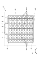
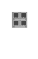
- FIG. 1 is a plan view of a photodiode array.
- FIG. 2 is an enlarged plan view of the photodiode array.
- 3 is a cross-sectional view of the photodiode array shown in FIG. 2 taken along line III-III.
- FIG. 4 is a cross-sectional view of the photodiode array shown in FIG. 2 taken along the line IV-IV.
- FIG. 5 is an enlarged plan view of the photodiode array. 6 is a cross-sectional view taken along the line VI-VI of the photodiode array shown in FIG. 7 is a cross-sectional view of the photodiode array shown in FIG. 5 taken along the line VII-VII.
- FIG. 8 is a plan view of the wiring.
- FIG. 8 is a plan view of the wiring.
- FIG. 9 is an enlarged plan view of the photodiode array.
- 10 is a cross-sectional view of the photodiode array shown in FIG. 9 taken along the line XX.
- 11 is a cross-sectional view taken along the line XI-XI of the photodiode array shown in FIG.
- FIG. 12 is an enlarged plan view of the photodiode array.
- 13 is a cross-sectional view of the photodiode array shown in FIG. 12 taken along the line XIII-XIII.
- 14 is a cross-sectional view taken along the line XIV-XIV of the photodiode array shown in FIG.
- FIG. 15 is an enlarged plan view of the photodiode array.
- FIG. 16 is a cross-sectional view of the photodiode array shown in FIG. 15 taken along the line XVI-XVI.
- 17 is a cross-sectional view of the photodiode array shown in FIG. 15 taken along the line XVII-XVII.
- FIG. 18 is an enlarged plan view of the photodiode array.
- 19 is a cross-sectional view of the photodiode array shown in FIG. 18 taken along the line XIX-XIX.
- 20 is a cross-sectional view taken along the line XX-XX of the photodiode array shown in FIG.
- FIG. 21 is an enlarged plan view of the photodiode array.
- 22 is a cross-sectional view of the photodiode array shown in FIG.
- FIG. 21 taken along the line XXII-XXII.
- FIG. 23 is a cross-sectional view of the photodiode array shown in FIG. 21 taken along the line XXIII-XXIII.
- FIG. 24 is a plan view of the photodiode array.
- 25 is a diagram showing a photomicrograph of the photodiode array shown in FIG. 26 is a diagram showing a photomicrograph of the photodiode array shown in FIG. 27 is a view showing a micrograph of the photodiode array shown in FIG.
- FIG. 28 is a view showing a photomicrograph of the photodiode array shown in FIG.
- FIG. 29 is a diagram showing a photomicrograph of the photodiode array shown in FIG. FIG.
- FIG. 30 is a view showing a photomicrograph of the photodiode array shown in FIG.
- FIG. 31 is a view showing a photomicrograph of the photodiode array shown in FIG.
- FIG. 32 is a view showing a photomicrograph of the photodiode array shown in FIG.
- FIG. 33 is a circuit diagram of the photodiode array.
- FIG. 34 is a diagram illustrating an equivalent circuit of a detection unit including an avalanche photodiode and a quenching resistor.
- FIG. 35 is a diagram showing a radiation detector provided with a photodiode array.
- FIG. 1 is a plan view of the photodiode array 10.
- the thickness direction of the photodiode array 10 coincides with the Z axis, and the light incident surface of the photodiode array 10 coincides with the XY plane.
- the photodiode array 10 includes a semiconductor substrate 20, the shape of the semiconductor substrate 20 is a rectangle, and each side is parallel to the X axis or the Y axis.
- the photodiode array 10 includes a plurality of avalanche photodiodes APD formed in the semiconductor substrate 20.
- a quenching resistor 7 is connected in series to each avalanche photodiode APD.
- the region where the plurality of avalanche photodiodes APD are formed is surrounded by the outer peripheral wiring WL.
- a light shielding layer SL made of metal or the like can be provided outside the outer peripheral wiring WL.
- the outer periphery of the outer peripheral wiring WL is a rectangular ring, and each side extends along the X axis or the Y axis, and is connected to the electrode pad P extending along the X axis.
- a plurality of relay wirings 8 are electrically connected to the outer peripheral wiring WL. Each of the plurality of relay wirings 8 extends along the Y axis, and connects between at least two locations (portions located at both ends along the Y axis) of the outer peripheral wiring WL.
- the resistance value per unit length of the outer peripheral wiring WL is smaller than the resistance value per unit length of the relay wiring 8. That is, when the outer peripheral wiring WL and the relay wiring 8 are made of the same conductive material (for example, aluminum) and the outer peripheral wiring WL extends along the Y axis, the area of the XZ cross section is the XZ cross section of the relay wiring 8. Greater than area. In addition, when the outer peripheral wiring WL extends along the X axis, the area of the YZ cross section is larger than the area of the XZ cross section of the relay wiring 8.
- FIG. 8 is a plan view of wiring. When the outer peripheral wiring WL and the relay wiring 8 have the same thickness, the width W1 of the outer peripheral wiring WL is wider than the width W2 of the relay wiring 8.
- One of the anode and the cathode of each avalanche photodiode APD is electrically connected to one of the relay wirings 8 via the quenching resistor 7, and the other of the anode and the cathode of each avalanche photodiode APD is a semiconductor. It is electrically connected to another electrode 6 provided on the substrate 20 (see FIG. 3: back electrode in this example). The other electrode 6 may be provided on the surface side of the semiconductor substrate 20 as long as it can be electrically connected to the other of the anode and the cathode.
- the photodiode array 10 includes the outer peripheral wiring WL
- the current from the avalanche photodiode APD is connected to the relay wiring 8 and the connection points between the relay wiring 8 and the outer peripheral wiring WL (two in this example). So that the larger one of them (the one with the lower resistance in the signal transmission path to the electrode pad P) flows through the outer peripheral wiring WL to the electrode pad P and is taken out to the outside.
- the outer peripheral wiring WL is provided, the resistance value in the signal readout path can be reduced, so that the time constant is reduced, and therefore the time resolution of the photodiode array can be improved.
- the current from the avalanche photodiode APD located at the lower left in FIG. 1 flows in the negative direction of the Y axis in the relay wiring 8, it flows into the connection point Q1 with the outer peripheral wiring WL as a bypass path, and then After traveling in the negative direction of the X-axis in the outer peripheral wiring WL, it proceeds along the positive direction of the Y-axis, and further travels along the positive direction of the X-axis and flows in many paths to the electrode pad P. It will be.
- the current from the avalanche photodiode APD located at the upper left in FIG. 1 flows in the positive direction of the Y axis in the relay wiring 8, and then flows into the connection point Q2 with the outer peripheral wiring WL as a bypass path, and thereafter In the outer peripheral wiring WL, it travels along the positive direction of the X axis and flows in a large amount along the path to the electrode pad P.
- the relay wiring 8 is connected in two places of the outer periphery wiring WL, this may have three or more connection points.
- the shape of the relay wiring 8 is a cruciform shape, it can be connected to the outer peripheral wiring WL at four locations. If the relay wiring 8 extends radially, bends, or branches, the connection location Can be 3 or more.
- a plurality of avalanche photodiodes APD are arranged on both sides of one relay wiring 8, and each of the avalanche photodiodes APD is connected to the relay wiring 8 via the quenching resistor 7. It is connected.
- the peripheral structure of the avalanche photodiode APD will be described in detail.
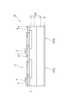
- FIG. 2 is an enlarged plan view of the first type photodiode array
- FIG. 3 is a cross-sectional view taken along the line III-III of the photodiode array shown in FIG. 2
- FIG. 4 is the photodiode array shown in FIG. FIG. 4 is a cross-sectional view taken along line IV-IV.
- the semiconductor substrate 20 includes a first semiconductor layer 1, a second semiconductor layer 2 formed on the first semiconductor layer 1, and a third semiconductor layer 3 formed in the second semiconductor layer 2. And.
- the conductivity types of the first semiconductor layer 1, the second semiconductor layer 2, and the third semiconductor layer 3 are the first conductivity type (N type), the second conductivity type (P type), and the second conductivity type (P type), respectively. ).
- a PN junction is formed between the first semiconductor layer 1 and the second semiconductor layer 2, and carriers generated in the depletion layer extending from the PN junction immediately below each ring electrode 5 are generated by the third semiconductor layer 3. And collected at each ring electrode 5.
- a reverse bias is applied to the avalanche photodiode APD composed of this PN junction.
- the second semiconductor layer 2 is preferably formed by epitaxial growth on the surface of the first semiconductor layer (substrate) 1 from the viewpoint of obtaining a good crystallinity.
- the third semiconductor layer 3 can be formed by ion implantation or diffusion of impurities into the second semiconductor layer 2.
- the semiconductor substrate 20 is preferably made of Si, and pentavalent antimony or phosphorus can be used as the N-type impurity, and trivalent boron can be used as the P-type impurity.
- the dimension (preferable range) of the ring-shaped electrode 5 is as follows. ⁇ Line width: 3 ⁇ m (2-5 ⁇ m) ⁇ X-axis dimension: 50 ⁇ m (10-100 ⁇ m) ⁇ Y-axis dimension: 50 ⁇ m (10-100 ⁇ m) Opening area: 2500 ⁇ m 2 (100 ⁇ m 2 to 10000 ⁇ m 2 )
- the conductivity types of the first semiconductor layer 1, the second semiconductor layer 2, and the third semiconductor layer 3 are the first conductivity type (N-type) and the first conductivity type, respectively. It is also possible to use a conductivity type (N type) or a second conductivity type (P type). In this case, a PN junction is formed between the second semiconductor layer 2 and the third semiconductor layer 3, and carriers generated in the depletion layer extending from the PN junction immediately below each ring electrode 5 are generated by the third semiconductor. Collected at each ring electrode 5 via layer 3. A reverse bias is applied to the avalanche photodiode APD composed of this PN junction.
- the first conductivity type may be P type and the second conductivity type may be N type.
- the bias application direction is opposite to the above. become.
- An insulating layer 4 made of SiO 2 is formed on the third semiconductor layer 3, and a ring electrode 5 is formed on the insulating layer 4.
- the ring electrode 5 is connected to the third semiconductor layer 3 through an opening provided in the insulating layer 4.
- the planar shape of the ring-shaped electrode 5 is a rectangular ring shape, and one end of the ring-shaped electrode 5 is connected to one end of a quenching resistor (layer) 7 through an appropriate conductive layer as necessary.
- the quenching resistor 7 extending along the X axis is made of polysilicon, and the ring electrode 5, the relay wiring 8 and the outer peripheral wiring are made of aluminum.
- the volume resistivity of polysilicon is higher than the volume resistivity of aluminum.
- the quenching resistor 7 is formed on the insulating layer 4, and the other end of the quenching resistor 7 is electrically connected to the relay wiring 8 extending along the Y axis.
- Another electrode 6 is provided on the back surface of the semiconductor substrate 20, but when the first semiconductor layer 1 is N-type, this electrode 6 becomes a cathode electrode, the ring electrode 5 becomes an anode electrode, Each region sandwiched between these electrodes constitutes an avalanche photodiode APD.
- a reverse bias voltage Vop is applied between the cathode electrode and the anode electrode.
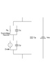
- FIG. 33 is a circuit diagram of the photodiode array.
- Each avalanche photodiode APD constituting the photodiode array is connected in parallel with each other in series with the quenching resistor 7, and a reverse bias voltage Vop is applied from the power source.
- An output current from the avalanche photodiode is detected by a detector A including an amplifier.
- FIG. 34 is a diagram showing an equivalent circuit of a detection unit including an avalanche photodiode and a quenching resistor.
- the avalanche photodiode APD is shown as a current source I and a capacitor Cd providing a diode capacitance connected in parallel
- the quenching resistance is shown as a resistance having a resistance value Rq
- a capacitor Cq is connected in parallel thereto,
- a capacitor Cg indicating a wiring capacity is connected in parallel with the power source.
- the presence of the capacitor Cq improves the time resolution of the photodiode array.
- a photodiode array including the capacitor Cq in various forms will be described. That is, the photodiode array of the following form further includes a quenching resistor Rq connected in series to each avalanche photodiode APD and a capacitor Cq connected in parallel to the quenching resistor Rq.
- FIG. 25 is a diagram showing a photomicrograph when the photodiode array shown in FIG. 2 is produced.
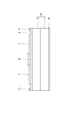
- FIG. 5 is an enlarged plan view of the photodiode array including the capacitor Cq
- FIG. 6 is a sectional view taken along the line VI-VI of the photodiode array shown in FIG. 5
- FIG. 7 is the photodiode array shown in FIG. FIG. 7 is a cross-sectional view taken along line VII-VII.
- a difference between the photodiode array of this example and the photodiode array shown in FIGS. 2 to 4 is that an outer peripheral region 9 is provided around the relay wiring 8 so as to surround the ring electrode 5. A part of is continuous to the intermediate wiring 11 and the width W2 of the relay wiring 8 is increased, and the other structure is the same. That is, in this photodiode array, one of the anode and the cathode of each avalanche photodiode APD is electrically connected to the ring electrode 5, but the relay wiring 8 is separated from the ring electrode 5, A conductive outer peripheral region 9 extending so as to surround the electrode 5 is provided.
- the outer peripheral region 9 is also made of aluminum.
- the capacitor Cq described above has the outer peripheral region 9 extending from the relay wiring 8 and the ring electrode 5, and a capacitance is formed between them.
- the capacitor can be configured in a planar manner, and the time resolution is improved.
- the width W2 of the relay wiring 8 is 9 ⁇ m, and preferably 2 to 10 ⁇ m. In this case, it is possible to sufficiently reduce the resistance value and suppress the output difference between the pixels. .
- intermediate wirings 11 extending in parallel to these are provided between the adjacent relay wirings 8. Both ends of the intermediate wiring 11 are connected to two locations of the outer peripheral wiring WL. Of course, the intermediate wiring 11 may be connected to three or more locations of the outer peripheral wiring WL. In addition, when using the below-mentioned crossing wiring, the end of the relay wiring 8 and the intermediate wiring 11 is connected to a crossing wiring. In the region outside the opening of the ring electrode 5, incident light is blocked by the relay wiring 8, the intermediate wiring 11, and the outer peripheral wiring WL. Can be returned. A part of the outer peripheral region 9 extending from the relay wiring 8 is continuous with the intermediate wiring 11, and the other part of the outer peripheral region 9 extends so as to be positioned between the quenching resistor 7 and the ring-shaped electrode 5. ing.
- FIG. 26 is a view showing a photomicrograph of the photodiode array shown in FIG. In this case, it was confirmed that the capacitor can be configured in a planar manner and the time resolution is improved.
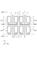
- FIG. 9 is an enlarged plan view of another photodiode array including a capacitor Cq
- FIG. 10 is a cross-sectional view of the photodiode array shown in FIG. 9, taken along line XX
- FIG. 11 is a photo of the photodiode array shown in FIG. It is XI-XI arrow sectional drawing of a diode array.
- each relay wiring 8 is connected to an outer peripheral region 9 on both sides, but there is no intermediate wiring 11.
- the adjacent outer peripheral regions 9 are separated from each other, and the other structures are the same. That is, the outer peripheral region 9 surrounds the ring-shaped electrode 5, but there is no intermediate wiring 11, and the distal end portion of the outer peripheral region 9 is separated from the adjacent outer peripheral region 9.
- the capacitor Cq is formed between the outer peripheral region 9 and the ring electrode 5.
- FIG. 27 is a view showing a photomicrograph of the photodiode array shown in FIG. Also in this case, it was confirmed that the capacitor can be configured in a planar manner and the time resolution is improved.
- FIG. 12 is an enlarged plan view of still another photodiode array including the capacitor Cq.
- FIG. 13 is a cross-sectional view of the photodiode array shown in FIG. 12 taken along the line XIII-XIII, and
- FIG. 4 is a cross-sectional view of the illustrated photodiode array taken along line XIV-XIV.
- each relay wiring 8 has an opening OP in a region along its center line (Y axis).
- the other structures are the same.
- the wiring capacity of the relay wiring 8 can be reduced, and the time resolution can be further improved.
- the width of the opening OP in the X-axis direction is 5 ⁇ m, and is preferably 2 to 5 ⁇ m from the viewpoint of further improving the time resolution.
- This opening structure can be applied to a structure including another relay wiring 8.
- FIG. 28 shows a photomicrograph of the photodiode array shown in FIG. Also in this case, it was confirmed that the capacitor can be configured in a planar manner and the time resolution is improved.
- FIG. 15 is an enlarged plan view of still another photodiode array including the capacitor Cq
- FIG. 16 is a cross-sectional view of the photodiode array shown in FIG. 15 taken along the line XVI-XVI
- FIG. 7 is a cross-sectional view of the illustrated photodiode array taken along line XVII-XVII.
- the difference between the photodiode array of this example and the photodiode array shown in FIGS. 2 to 5 is that a capacitor Cq is formed on the quenching resistor 7 via an insulating layer K such as SiN or SiO 2.
- the coated wiring K1 is provided, and one end of the coated wiring K1 is electrically connected to one end of the quenching resistor 7, and the other structure is the same.
- the covered wiring K1 extends from the relay wiring 8 and covers the insulating layer K. A capacitance is formed between the covered wiring K1 and the quenching resistor 7.
- FIG. 29 is a view showing a photomicrograph of the photodiode array shown in FIG. Even in this case, since the capacitor can be three-dimensionally formed by stacking, it was confirmed that the element density can be improved and the time resolution is improved.
- FIG. 18 is an enlarged plan view of still another photodiode array including the capacitor Cq
- FIG. 19 is a cross-sectional view of the photodiode array shown in FIG. 18, taken along the line XIX-XIX
- FIG. 19 is a cross-sectional view of the photodiode array shown in FIG. 18 taken along line XX-XX.
- the difference between the photodiode array of this example and the photodiode array shown in FIGS. 15 to 17 is that the covered wiring K1 extends from the ring electrode 5 and covers the insulating layer K. Other configurations are the same. In this case as well, a capacitance is formed between the covered wiring K1 and the quenching resistor 7 to configure the capacitor Cq.
- FIG. 30 is a view showing a micrograph of the photodiode array shown in FIG. Even in this case, since the capacitor can be three-dimensionally formed by stacking, it was confirmed that the element density can be improved and the time resolution is improved.
- FIG. 21 is an enlarged plan view of still another photodiode array including the capacitor Cq
- FIG. 22 is a cross-sectional view of the photodiode array shown in FIG. 21, taken along line XXII-XXII
- FIG. 22 is a cross-sectional view of the photodiode array shown in FIG. 21 taken along line XXIII-XXIII.
- FIG. 31 is a view showing a photomicrograph of the photodiode array shown in FIG.
- FIG. 24 is a plan view of the photodiode array.
- This photodiode array 10 is obtained by adding a transverse wiring WL2 to the one shown in FIG. 1 and inverting the top and bottom of the avalanche photodiode group located above the transverse wiring WL2 in the drawing. This is the same as that shown in FIG.
- the transverse wiring WL2 is electrically connected to the outer peripheral wiring WL, and connects at least two locations of the outer peripheral wiring WL.
- the transverse wiring WL2 extends along the X axis, and the width thereof is larger than the width of the relay wiring 8.
- the resistance value per unit length of the transverse wiring WL2 is smaller than the resistance value per unit length of the relay wiring 8.
- one end of each relay wiring 8 shown in FIG. 1 is electrically connected to the transverse wiring WL2 instead of the outer peripheral wiring WL.
- the width of the transverse wiring WL2 is 20 ⁇ m, and is preferably 10 to 30 ⁇ m from the viewpoint of improving time resolution.
- FIG. 32 is a view showing a photomicrograph of the photodiode array shown in FIG.
- FIGS. 3 to 23 the structure including the transverse wiring WL2 shown in FIG. 24 is also shown in FIGS. Applicable to structure.
- jitter at 10 mV of the output waveform was measured.
- the jitter is 146 ps (type 1).
- the outer peripheral wiring WL is as thick as the relay wiring 8 (as a comparative example)
- the jitter is 160 ps.
- the jitter was 148 ps (type 2). It has been found that jitter is reduced and time resolution is significantly improved as compared with the comparative example.
- the jitter is 142 ps (type 3).
- the jitter is 138 ps (type 4).
- the jitter was 130 ps (type 5).
- the jitter was 125 ps (type 6).
- the jitter is 127 ps (type 7).
- the jitter was 146 ps (type 8).
- type 2 transverse wiring can be used in type 3 to type 8 structures. It is also possible to combine any structure of types 3 to 5 and any structure of types 6 to 8, and the structure of type 8 can be combined with any type of structure. In particular, when Type 5 (opening structure) or Type 8 (vertically long structure) is combined with Type 6 or 7 structure (laminated structure), the above-mentioned effects are synergistic and it is possible to further reduce jitter. It is done.
- FIG. 35 is a view showing a radiation detector provided with a photodiode array.
- a scintillator panel is fixed on the light incident surface of the photodiode array 10.
- the scintillator panel includes a scintillator 11 such as CsI and a coating layer 12 such as polyparaxylylene that covers the scintillator. 13 is interposed.
- the scintillator 11 emits light, and this light enters the photodiode array 10.
- a reverse bias voltage exceeding the breakdown voltage is applied to the photodiode array 10 between the electrode P and the electrode 6, and the output can be detected via the detector A.
- a radiation detector excellent in time resolution can be applied to an X-ray CT, a PET apparatus, or the like, and can measure an image having a resolution that could not be measured so far.
- SYMBOLS 10 ... Photodiode array, 1 ... 1st semiconductor layer, 2 ... 2nd semiconductor layer, 3 ... 3rd semiconductor layer, 4 ... Insulating layer, 5 ... Ring-shaped electrode, 6 ... Another electrode, 7 ... Quenching resistance, 8 ... Relay wiring, PD ... Photodiode, WL ... Outer peripheral wiring, 9 ... Outer peripheral area, 11 ... Intermediate wiring , WL2 ... transverse wiring.
Abstract
Description
Emission Tomography)装置等の検出器として用いることが有望視されている。PET装置における光子の計測においては、更に高い時間分解能が要求されている。時間分解能を向上させるには、MPPCから出力波形の形状を鋭くする必要がある。下記非特許文献1には、クエンチング抵抗に対して、並列な容量(Cq)を付加することで、出力パルスが鋭くなり、時間分解能が向上することが示されている。 Since MPPC has better time characteristics than other detectors, it uses the Time-Of-Flight (TOF) measurement method PET (Positron
Emission Tomography) is expected to be used as a detector for devices. In photon measurement in a PET apparatus, higher time resolution is required. In order to improve the time resolution, it is necessary to sharpen the shape of the output waveform from the MPPC. Non-Patent
・線幅:3μm(2~5μm)
・X軸方向寸法:50μm(10~100μm)
・Y軸方向寸法:50μm(10~100μm)
・開口面積:2500μm2(100μm2~10000μm2) Moreover, the dimension (preferable range) of the ring-shaped
・ Line width: 3μm (2-5μm)
・ X-axis dimension: 50μm (10-100μm)
・ Y-axis dimension: 50μm (10-100μm)
Opening area: 2500 μm 2 (100 μm 2 to 10000 μm 2 )
・抵抗値Rq:150kΩ(50~300kΩ)
・キャパシタCgの容量:5pF(配線容量であり0が好ましく、小さい程よい)
上記の場合、時間分解能が更に向上する。図25は、図2に示したフォトダイオードアレイを作製した場合の顕微鏡写真を示す図である。 The resistance value Rq (preferable range) and the capacitance of the capacitor Cg (preferable range) are as follows.
・ Resistance value Rq: 150kΩ (50-300kΩ)
Capacitance of capacitor Cg: 5 pF (wiring capacitance, 0 is preferable, and smaller is better)
In the above case, the time resolution is further improved. FIG. 25 is a diagram showing a photomicrograph when the photodiode array shown in FIG. 2 is produced.
Claims (9)
- フォトダイオードアレイにおいて、
半導体基板内に形成された複数のアバランシェフォトダイオードと、
それぞれのアバランシェフォトダイオードに対して直列に接続されたクエンチング抵抗と、
複数の前記アバランシェフォトダイオードが形成された領域を囲む外周配線と、
前記外周配線に電気的に接続され、前記外周配線の少なくとも2箇所間をそれぞれが接続する複数の中継配線と、
を備え、
前記外周配線の単位長さ当たりの抵抗値は、前記中継配線の単位長さ当たりの抵抗値よりも小さく、
個々の前記アバランシェフォトダイオードのアノード及びカソードの一方は、前記クエンチング抵抗を介して、前記中継配線のいずれかに電気的に接続され、
個々の前記アバランシェフォトダイオードのアノード及びカソードの他方は、前記半導体基板に設けられた別の電極に電気的に接続されている、
ことを特徴とするフォトダイオードアレイ。 In the photodiode array,
A plurality of avalanche photodiodes formed in a semiconductor substrate;
A quenching resistor connected in series with each avalanche photodiode;
A peripheral wiring surrounding a region where a plurality of the avalanche photodiodes are formed;
A plurality of relay wirings electrically connected to the outer peripheral wiring, each connecting at least two locations of the outer peripheral wiring;
With
The resistance value per unit length of the outer peripheral wiring is smaller than the resistance value per unit length of the relay wiring,
One of the anode and the cathode of each of the avalanche photodiodes is electrically connected to one of the relay wirings via the quenching resistor,
The other of the anode and the cathode of each of the avalanche photodiodes is electrically connected to another electrode provided on the semiconductor substrate.
A photodiode array. - 前記外周配線に電気的に接続され、前記外周配線の少なくとも2箇所間を接続し、前記中継配線の単位長さ当たりの抵抗値よりも、自身の単位長さ当たりの抵抗値が小さい横断配線を更に備え、
それぞれの前記中継配線の一端は、前記外周配線に代えて、前記横断配線に電気的に接続されていることを特徴とする請求項1に記載のフォトダイオードアレイ。 A transverse wiring electrically connected to the outer peripheral wiring, connected between at least two locations of the outer peripheral wiring, and having a resistance value per unit length smaller than a resistance value per unit length of the relay wiring In addition,
2. The photodiode array according to claim 1, wherein one end of each of the relay wirings is electrically connected to the transverse wiring instead of the outer peripheral wiring. - それぞれの前記クエンチング抵抗にそれぞれ並列に接続されたキャパシタを更に備えていることを特徴とする請求項1又は2に記載のフォトダイオードアレイ。 3. The photodiode array according to claim 1, further comprising a capacitor connected in parallel to each of the quenching resistors.
- それぞれの前記アバランシェフォトダイオードのアノード及びカソードの一方は、リング状電極に電気的に接続されており、
前記中継配線は、前記リング状電極から離間し、前記リング状電極を囲むように延びた導電性の外周領域を備えており、
前記キャパシタは、
前記中継配線から延びた前記外周領域と、
前記リング状電極と、を有していることを特徴とする請求項3に記載のフォトダイオードアレイ。 One of the anode and the cathode of each of the avalanche photodiodes is electrically connected to a ring electrode,
The relay wiring is provided with a conductive outer peripheral region that is separated from the ring electrode and extends to surround the ring electrode.
The capacitor is
The outer peripheral region extending from the relay wiring;
The photodiode array according to claim 3, comprising the ring-shaped electrode. - 前記中継配線間に平行に延びた中間配線を更に備え、
前記中間配線は、前記外周配線の少なくとも2箇所間をそれぞれが接続しており、
前記外周領域は、前記中間配線に連続していることを特徴とする請求項4に記載のフォトダイオードアレイ。 Further comprising an intermediate wiring extending in parallel between the relay wiring,
The intermediate wiring is connected between at least two locations of the outer peripheral wiring,
The photodiode array according to claim 4, wherein the outer peripheral region is continuous with the intermediate wiring. - それぞれの前記中継配線には、その両側に前記外周領域が接続されており、
互いに隣接する前記中継配線に関して、互いに隣接する前記外周領域は離間していることを特徴とする請求項4に記載のフォトダイオードアレイ。 Each of the relay wires is connected to the outer peripheral region on both sides thereof,
The photodiode array according to claim 4, wherein the outer peripheral regions adjacent to each other are separated from each other with respect to the relay wirings adjacent to each other. - それぞれの前記中継配線は、その中心線に沿った領域が開口していることを特徴とする請求項3に記載のフォトダイオードアレイ。 4. The photodiode array according to claim 3, wherein each of the relay wirings has an opening along a center line thereof.
- 前記キャパシタは、前記クエンチング抵抗上に、絶縁層を介して、形成された被覆配線を有しており、この被覆配線の一端は、前記クエンチング抵抗の一端に電気的に接続されていることを特徴とする請求項3乃至7のいずれか1項に記載のフォトダイオードアレイ。 The capacitor has a covered wiring formed on the quenching resistor via an insulating layer, and one end of the covered wiring is electrically connected to one end of the quenching resistor. The photodiode array according to any one of claims 3 to 7.
- それぞれの前記アバランシェフォトダイオードのアノード及びカソードの一方は、リング状電極に電気的に接続されており、
前記リング状電極のアスペクト比は、2以上であることを特徴とする請求項3に記載のフォトダイオードアレイ。 One of the anode and the cathode of each of the avalanche photodiodes is electrically connected to a ring electrode,
4. The photodiode array according to claim 3, wherein the ring electrode has an aspect ratio of 2 or more.
Priority Applications (4)
| Application Number | Priority Date | Filing Date | Title |
|---|---|---|---|
| EP11836216.9A EP2634821B1 (en) | 2010-10-29 | 2011-10-24 | Photodiode array |
| KR1020137011542A KR101830464B1 (en) | 2010-10-29 | 2011-10-24 | Photodiode array |
| CN201180052213.3A CN103190000B (en) | 2010-10-29 | 2011-10-24 | Photodiode array |
| US13/881,949 US9184190B2 (en) | 2010-10-29 | 2011-10-24 | Photodiode array |
Applications Claiming Priority (2)
| Application Number | Priority Date | Filing Date | Title |
|---|---|---|---|
| JP2010-244686 | 2010-10-29 | ||
| JP2010244686A JP5562207B2 (en) | 2010-10-29 | 2010-10-29 | Photodiode array |
Publications (1)
| Publication Number | Publication Date |
|---|---|
| WO2012057082A1 true WO2012057082A1 (en) | 2012-05-03 |
Family
ID=45993790
Family Applications (1)
| Application Number | Title | Priority Date | Filing Date |
|---|---|---|---|
| PCT/JP2011/074437 WO2012057082A1 (en) | 2010-10-29 | 2011-10-24 | Photodiode array |
Country Status (7)
| Country | Link |
|---|---|
| US (1) | US9184190B2 (en) |
| EP (1) | EP2634821B1 (en) |
| JP (1) | JP5562207B2 (en) |
| KR (1) | KR101830464B1 (en) |
| CN (1) | CN103190000B (en) |
| TW (1) | TWI518933B (en) |
| WO (1) | WO2012057082A1 (en) |
Cited By (5)
| Publication number | Priority date | Publication date | Assignee | Title |
|---|---|---|---|---|
| JP2014090034A (en) * | 2012-10-29 | 2014-05-15 | Hamamatsu Photonics Kk | Photodiode array |
| JP2014160042A (en) * | 2013-02-20 | 2014-09-04 | Hamamatsu Photonics Kk | Detector, pet apparatus, and x-ray ct device |
| WO2015093482A1 (en) * | 2013-12-19 | 2015-06-25 | 浜松ホトニクス株式会社 | Optical detector |
| WO2015022580A3 (en) * | 2013-08-13 | 2015-08-06 | Zecotek Photonics Inc. | Multi-pixel avalanche photodiode |
| JP2016192551A (en) * | 2016-04-20 | 2016-11-10 | 浜松ホトニクス株式会社 | Detector, pet apparatus and x-ray ct device |
Families Citing this family (26)
| Publication number | Priority date | Publication date | Assignee | Title |
|---|---|---|---|---|
| JP5731344B2 (en) * | 2011-09-28 | 2015-06-10 | 浜松ホトニクス株式会社 | Radiation detector |
| JP5926921B2 (en) * | 2011-10-21 | 2016-05-25 | 浜松ホトニクス株式会社 | Photodetector |
| JP5832852B2 (en) * | 2011-10-21 | 2015-12-16 | 浜松ホトニクス株式会社 | Photodetector |
| JP5791461B2 (en) | 2011-10-21 | 2015-10-07 | 浜松ホトニクス株式会社 | Photodetector |
| JP5995508B2 (en) * | 2012-04-27 | 2016-09-21 | キヤノン株式会社 | Semiconductor device and manufacturing method of semiconductor device |
| US8937285B2 (en) * | 2012-06-18 | 2015-01-20 | General Electric Company | Methods and systems for signal communication in gamma ray detectors |
| JP5984617B2 (en) * | 2012-10-18 | 2016-09-06 | 浜松ホトニクス株式会社 | Photodiode array |
| JP6383516B2 (en) * | 2013-04-19 | 2018-08-29 | ライトスピン テクノロジーズ、インク. | Integrated avalanche photodiode array |
| JP6319426B2 (en) * | 2014-03-31 | 2018-05-09 | 株式会社ニコン | DETECTING DEVICE, ELECTRONIC DEVICE, AND MANUFACTURING METHOD |
| KR102419715B1 (en) | 2014-06-09 | 2022-07-13 | 가부시키가이샤 한도오따이 에네루기 켄큐쇼 | Imaging device |
| JP2016122716A (en) * | 2014-12-24 | 2016-07-07 | 株式会社東芝 | Optical detection device and ct apparatus including the optical detection device |
| EP3396723A4 (en) * | 2015-12-21 | 2019-08-07 | Hamamatsu Photonics K.K. | Photoelectric conversion element and photoelectric conversion module |
| JP6650261B2 (en) * | 2015-12-21 | 2020-02-19 | 浜松ホトニクス株式会社 | Photoelectric conversion element |
| JP6543565B2 (en) * | 2015-12-21 | 2019-07-10 | 浜松ホトニクス株式会社 | PHOTOELECTRIC CONVERSION ELEMENT AND PHOTOELECTRIC CONVERSION MODULE |
| JP6734644B2 (en) * | 2015-12-21 | 2020-08-05 | 浜松ホトニクス株式会社 | Photoelectric conversion device |
| EP3258228B1 (en) * | 2016-06-17 | 2018-05-09 | Sick Ag | Light receiving device with avalanche photodiodes in geiger mode and method for reading |
| CN106298816A (en) * | 2016-10-11 | 2017-01-04 | 天津大学 | The single-photon avalanche diode of integrated cancellation resistance and manufacture method thereof |
| JP6884948B2 (en) * | 2017-03-17 | 2021-06-09 | 国立研究開発法人情報通信研究機構 | High speed photo detector array |
| KR101777657B1 (en) | 2017-03-22 | 2017-09-14 | 홍익대학교 산학협력단 | Quenching circuit |
| CN107275433B (en) * | 2017-03-29 | 2018-12-04 | 湖北京邦科技有限公司 | A kind of novel semi-conductor photo multiplier device |
| WO2019146725A1 (en) * | 2018-01-26 | 2019-08-01 | 浜松ホトニクス株式会社 | Photodetector device |
| JP7366558B2 (en) * | 2019-03-13 | 2023-10-23 | 株式会社東芝 | Sensor and distance measuring device |
| TWI819073B (en) * | 2019-08-22 | 2023-10-21 | 晶元光電股份有限公司 | Light-emitting device, manufacturing method thereof and display module using the same |
| DE102020120788B3 (en) * | 2020-08-06 | 2021-12-09 | Helmholtz-Zentrum Dresden - Rossendorf E. V. | MULTIPIXEL PHOTODETECTOR WITH AVALANCHE PHOTODIODS, RADIATION DETECTOR AND POSITRON EMISSION TOMOGRAPH |
| KR102610700B1 (en) * | 2021-05-25 | 2023-12-06 | 주식회사 우리로 | Method for Aligning the Avalanche Photodiode to an Optimal Position for Detecting Photons |
| JP2023112469A (en) * | 2022-02-01 | 2023-08-14 | 浜松ホトニクス株式会社 | photodetector |
Citations (4)
| Publication number | Priority date | Publication date | Assignee | Title |
|---|---|---|---|---|
| JP2002033965A (en) * | 2000-07-13 | 2002-01-31 | Fuji Film Microdevices Co Ltd | Drive circuit for solid-state image pickup element, and solid-state image sensing element having drive circuit |
| JP2005045125A (en) * | 2003-07-24 | 2005-02-17 | Hamamatsu Photonics Kk | Manufacturing method of photodetector |
| WO2008004547A1 (en) * | 2006-07-03 | 2008-01-10 | Hamamatsu Photonics K.K. | Photodiode array |
| JP2008103614A (en) * | 2006-10-20 | 2008-05-01 | Mitsui Eng & Shipbuild Co Ltd | Photoelectric transducer device |
Family Cites Families (8)
| Publication number | Priority date | Publication date | Assignee | Title |
|---|---|---|---|---|
| JP4841834B2 (en) | 2004-12-24 | 2011-12-21 | 浜松ホトニクス株式会社 | Photodiode array |
| JP2007071823A (en) | 2005-09-09 | 2007-03-22 | Sharp Corp | Light receiving element, and sensor and electronic device having it |
| US7652257B2 (en) | 2007-06-15 | 2010-01-26 | General Electric Company | Structure of a solid state photomultiplier |
| US8110806B2 (en) | 2008-10-31 | 2012-02-07 | General Electric Company | Solid-state photomultiplier having improved timing resolution |
| IT1392366B1 (en) | 2008-12-17 | 2012-02-28 | St Microelectronics Rousset | OPERATING PHOTODIODO IN GEIGER MODE WITH INTEGRATED AND CONTROLLABLE SUPPRESSION RESISTOR, PHOTODIUM RING AND RELATIVE PROCESS OF PROCESSING |
| JP5185205B2 (en) * | 2009-02-24 | 2013-04-17 | 浜松ホトニクス株式会社 | Semiconductor photo detector |
| JP2010278045A (en) * | 2009-05-26 | 2010-12-09 | Panasonic Corp | Optical semiconductor device |
| CN101789040B (en) | 2010-01-27 | 2011-09-14 | 中国科学院上海技术物理研究所 | Design method of Geiger mode angular position digitizer (APD) passive quenching and recovering integrated circuit |
-
2010
- 2010-10-29 JP JP2010244686A patent/JP5562207B2/en active Active
-
2011
- 2011-10-24 CN CN201180052213.3A patent/CN103190000B/en active Active
- 2011-10-24 KR KR1020137011542A patent/KR101830464B1/en active IP Right Grant
- 2011-10-24 EP EP11836216.9A patent/EP2634821B1/en active Active
- 2011-10-24 US US13/881,949 patent/US9184190B2/en active Active
- 2011-10-24 WO PCT/JP2011/074437 patent/WO2012057082A1/en active Application Filing
- 2011-10-27 TW TW100139163A patent/TWI518933B/en active
Patent Citations (4)
| Publication number | Priority date | Publication date | Assignee | Title |
|---|---|---|---|---|
| JP2002033965A (en) * | 2000-07-13 | 2002-01-31 | Fuji Film Microdevices Co Ltd | Drive circuit for solid-state image pickup element, and solid-state image sensing element having drive circuit |
| JP2005045125A (en) * | 2003-07-24 | 2005-02-17 | Hamamatsu Photonics Kk | Manufacturing method of photodetector |
| WO2008004547A1 (en) * | 2006-07-03 | 2008-01-10 | Hamamatsu Photonics K.K. | Photodiode array |
| JP2008103614A (en) * | 2006-10-20 | 2008-05-01 | Mitsui Eng & Shipbuild Co Ltd | Photoelectric transducer device |
Non-Patent Citations (2)
| Title |
|---|
| H. OTONO ET AL.: "On the basic mechanism of Pixelized Photon Detectors", NUCL. INSTR. AND METH., vol. A610, 2009, pages 397 |
| PIEMONTE ET AL.: "Characterization of the First Prototypes of Silicon Photomultiplier Fabricated at ITC-irst", IEEE TRANS. NUCL. SCI., vol. 54, no. 1, February 2007 (2007-02-01), pages 236 - 244, XP011163938 * |
Cited By (11)
| Publication number | Priority date | Publication date | Assignee | Title |
|---|---|---|---|---|
| JP2014090034A (en) * | 2012-10-29 | 2014-05-15 | Hamamatsu Photonics Kk | Photodiode array |
| JP2014160042A (en) * | 2013-02-20 | 2014-09-04 | Hamamatsu Photonics Kk | Detector, pet apparatus, and x-ray ct device |
| US10879303B2 (en) | 2013-02-20 | 2020-12-29 | Hamamatsu Photonics K.K. | Detector, PET system and X-ray CT system |
| US11101315B2 (en) | 2013-02-20 | 2021-08-24 | Hamamatsu Photonics K.K. | Detector, PET system and X-ray CT system |
| WO2015022580A3 (en) * | 2013-08-13 | 2015-08-06 | Zecotek Photonics Inc. | Multi-pixel avalanche photodiode |
| US9252317B2 (en) | 2013-08-13 | 2016-02-02 | Zecotek Photonics Inc. | Multi-pixel avalanche transistor |
| JP2016530722A (en) * | 2013-08-13 | 2016-09-29 | ゼコテック フォトニクス インコーポレイテッドZecotek Photonics Inc. | Multi-pixel avalanche photodiode |
| WO2015093482A1 (en) * | 2013-12-19 | 2015-06-25 | 浜松ホトニクス株式会社 | Optical detector |
| JP2015119093A (en) * | 2013-12-19 | 2015-06-25 | 浜松ホトニクス株式会社 | Photodetector |
| US9825083B2 (en) | 2013-12-19 | 2017-11-21 | Hamamatsu Photonics K.K. | Optical detector with photodiode array having avalanche photodiodes connected to quenching resistors |
| JP2016192551A (en) * | 2016-04-20 | 2016-11-10 | 浜松ホトニクス株式会社 | Detector, pet apparatus and x-ray ct device |
Also Published As
| Publication number | Publication date |
|---|---|
| KR20140001889A (en) | 2014-01-07 |
| TWI518933B (en) | 2016-01-21 |
| KR101830464B1 (en) | 2018-02-20 |
| TW201232800A (en) | 2012-08-01 |
| US20130270666A1 (en) | 2013-10-17 |
| US9184190B2 (en) | 2015-11-10 |
| JP2012099580A (en) | 2012-05-24 |
| EP2634821A4 (en) | 2017-12-27 |
| JP5562207B2 (en) | 2014-07-30 |
| CN103190000A (en) | 2013-07-03 |
| EP2634821B1 (en) | 2018-11-21 |
| EP2634821A1 (en) | 2013-09-04 |
| CN103190000B (en) | 2015-09-09 |
Similar Documents
| Publication | Publication Date | Title |
|---|---|---|
| JP5562207B2 (en) | Photodiode array | |
| US11101315B2 (en) | Detector, PET system and X-ray CT system | |
| JP5832852B2 (en) | Photodetector | |
| JP5254066B2 (en) | Imaging detector | |
| JP6839712B2 (en) | Photodetector | |
| US8860166B2 (en) | Photo detector array of geiger mode avalanche photodiodes for computed tomography systems | |
| JP6839713B2 (en) | Photodetector | |
| JP2015084392A (en) | Photo-detector | |
| CN109313072B (en) | Light detection unit, light detection device, and method for manufacturing light detection unit | |
| US9054260B2 (en) | Radiation detecting element and radiation detecting device | |
| TWI586990B (en) | Photodetector | |
| JP2016192551A (en) | Detector, pet apparatus and x-ray ct device | |
| JPH07122776A (en) | Light-radiation-electricity conversion semiconductor device and application thereof | |
| JP2020096157A (en) | Light detecting device | |
| JP5823813B2 (en) | Radiation detector | |
| TWI675219B (en) | Detector | |
| JP6948668B2 (en) | Neutron semiconductor detector |
Legal Events
| Date | Code | Title | Description |
|---|---|---|---|
| 121 | Ep: the epo has been informed by wipo that ep was designated in this application |
Ref document number: 11836216 Country of ref document: EP Kind code of ref document: A1 |
|
| NENP | Non-entry into the national phase |
Ref country code: DE |
|
| ENP | Entry into the national phase |
Ref document number: 20137011542 Country of ref document: KR Kind code of ref document: A |
|
| WWE | Wipo information: entry into national phase |
Ref document number: 2011836216 Country of ref document: EP |
|
| WWE | Wipo information: entry into national phase |
Ref document number: 13881949 Country of ref document: US |