WO2012056889A1 - 可変容量装置 - Google Patents
可変容量装置 Download PDFInfo
- Publication number
- WO2012056889A1 WO2012056889A1 PCT/JP2011/073491 JP2011073491W WO2012056889A1 WO 2012056889 A1 WO2012056889 A1 WO 2012056889A1 JP 2011073491 W JP2011073491 W JP 2011073491W WO 2012056889 A1 WO2012056889 A1 WO 2012056889A1
- Authority
- WO
- WIPO (PCT)
- Prior art keywords
- movable
- capacitance
- support plate
- capacity
- drive
- Prior art date
- Legal status (The legal status is an assumption and is not a legal conclusion. Google has not performed a legal analysis and makes no representation as to the accuracy of the status listed.)
- Ceased
Links
Images


Classifications
-
- H—ELECTRICITY
- H01—ELECTRIC ELEMENTS
- H01G—CAPACITORS; CAPACITORS, RECTIFIERS, DETECTORS, SWITCHING DEVICES, LIGHT-SENSITIVE OR TEMPERATURE-SENSITIVE DEVICES OF THE ELECTROLYTIC TYPE
- H01G5/00—Capacitors in which the capacitance is varied by mechanical means, e.g. by turning a shaft; Processes of their manufacture
- H01G5/16—Capacitors in which the capacitance is varied by mechanical means, e.g. by turning a shaft; Processes of their manufacture using variation of distance between electrodes
- H01G5/18—Capacitors in which the capacitance is varied by mechanical means, e.g. by turning a shaft; Processes of their manufacture using variation of distance between electrodes due to change in inclination, e.g. by flexing, by spiral wrapping
-
- H—ELECTRICITY
- H01—ELECTRIC ELEMENTS
- H01G—CAPACITORS; CAPACITORS, RECTIFIERS, DETECTORS, SWITCHING DEVICES, LIGHT-SENSITIVE OR TEMPERATURE-SENSITIVE DEVICES OF THE ELECTROLYTIC TYPE
- H01G5/00—Capacitors in which the capacitance is varied by mechanical means, e.g. by turning a shaft; Processes of their manufacture
- H01G5/01—Details
Definitions
- the present invention relates to a variable capacitance device that controls an RF (Radio Frequency) capacitance using MEMS (Micro Electro Mechanical Systems) driven by electrostatic force.
- RF Radio Frequency
- MEMS Micro Electro Mechanical Systems
- the movable beam is elastically supported so as to face the support plate, and one or a plurality of pairs of counter electrodes are provided on the movable beam and the support plate.
- a bias voltage By applying a bias voltage to the counter electrode pair, an electrostatic attractive force is generated between the counter electrode pair, and the movable beam is deformed so that the electrostatic attractive force comes close to the movable beam and the support plate.
- the variable capacitance RF capacitance
- Patent Document 1 discloses a switching capacitor device.
- this switching capacitor device the entire surface of the movable beam is brought close to or separated from the support plate, and thereby the variable capacitor (RF capacitor) is controlled to be turned on or off.
- This switching capacitor device has a drive capacitor electrode pair and a variable capacitor electrode pair as counter electrode pairs.
- the drive capacitor electrode pair and the variable capacitor electrode pair are arranged in the main axis direction connecting between the support positions (anchors) of the movable beams, and the variable capacitor electrode pair is disposed between the two drive capacitor electrode pairs.
- variable capacitance device In a variable capacitance device or switching capacitor device using MEMS driven by electrostatic force, the deformation of the movable beam is caused not only by the bias voltage but also by the RF signal. This phenomenon is called self-activation, and the magnitude of electrostatic attraction and the amount of deformation of the movable beam due to self-activation are in accordance with the magnitude of the power (amplitude) of the RF signal. Therefore, in the variable capacitance device, when the power of the applied RF signal varies, the proximity state between the movable beam and the support plate also varies, and the drive capacitance and variable capacitance (RF capacitance) also vary. In particular, when the power of the applied RF signal becomes excessive, the drive capacity and variable capacity (RF capacity) become larger than desired values, and the control accuracy of the variable capacity (RF capacity) decreases.
- an object of the present invention is to prevent the capacitance correlation between the drive capacitance and the variable capacitance (RF capacitance) from fluctuating due to the effect of self-activation, and to improve the control accuracy of the variable capacitance (RF capacitance). It is an object of the present invention to provide a variable capacitance device having a configuration that can be configured.
- the variable capacity device of the present invention includes a support plate, a movable beam, a drive capacity section, and a variable capacity section.
- the movable beam includes a movable part, an anchor part, and a connecting part.
- the movable portion is supported to face the support plate, the anchor portion is fixed to the support plate, and the connecting portion connects the anchor portion and the movable portion.
- the drive capacity unit generates an electrostatic force that deforms the movable unit so as to be close to the support plate in a region where the movable unit and the support plate are opposed to each other.
- the size of the capacity of the variable capacitance portion changes according to the state in which the movable portion and the support plate are close to each other in a region where the movable portion and the support plate are opposed to each other.
- the drive capacity part and the variable capacity part are arranged adjacent to each other in the beam width direction of the movable beam.
- the connecting portion is connected to the movable portion at a position overlapping the end portion of the drive capacity portion on the variable capacity portion side or at a position closer to the variable capacity portion than the end portion.
- a drive capacitance is generated by applying a bias voltage, and an RF capacitance is also generated by applying an RF signal. Then, in addition to the electrostatic attractive force due to the driving capacity, the electrostatic attractive force due to the RF capacity also acts on the movable beam.
- the drive capacity section and the variable capacity section are adjacent to each other in the beam width direction, there is a deviation between the action point of electrostatic attraction in the beam width direction and the connection position of the connection section. The moment load acts. This moment load deflects the movable part in the beam width direction.
- the electrostatic attractive force due to the RF capacitance changes due to the influence of self-activation, the amount of bending in the beam width direction of the movable part also changes. If the amount of deflection in the beam width direction of the movable part varies, the capacity correlation varies between the drive capacity and the RF capacity.
- the moment load due to the electrostatic attractive force acting on the variable capacitance portion is reduced by the configuration in which the connection portion is connected in the vicinity of the variable capacitance portion. Then, even if the electrostatic attractive force acting on the variable capacitance portion varies due to the self-activation, the variation of the moment weight due to the electrostatic attractive force is suppressed. Thereby, the amount of bending in the beam width direction in the movable portion is stabilized, and the capacity correlation can be stabilized.
- the coupling portion is coupled to a position overlapping the end portion on the variable capacitance portion side of the drive capacitance portion.
- the movable beam deforms with the anchor portion as a fulcrum and the proximity area between the movable portion and the support plate expands, it is difficult to make the connection portion completely close to the connection portion.
- the surrounding area tends to rise from the support plate. Therefore, if the connecting portion is connected to the variable capacitance portion, it is difficult to make the variable capacitance portion completely close to the support plate, which causes a reduction in the maximum value of the RF capacitance. Therefore, in the above configuration, the position where the movable portion and the connecting portion are connected is located away from the variable capacitance portion but close to the variable capacitance portion, thereby preventing the maximum value of the RF capacitance from being reduced and reducing the RF capacitance.
- the capacity correlation can be stabilized while increasing the maximum value.
- the movable portion has a region where the drive capacitance portion is formed protrudes toward the anchor portion. With this configuration, it is possible to more reliably prevent the maximum value of the RF capacity from being reduced.
- the coupling portion is coupled to a side surface of the drive capacitance portion facing the variable capacitance portion side.
- variable capacitance device according to the embodiment of the present invention will be described with reference to the drawings.
- the XYZ axes in the orthogonal coordinate form with the thickness direction of the movable beam being the Z-axis direction, the length direction of the movable beam being the X-axis direction, and the width direction of the movable beam being the Y-axis direction. Is added.
- FIG. 1A is a plan view (XY plane plan view) of the variable capacitance device 1 according to the present embodiment.
- FIG. 1B is a cross-sectional view (XZ plane cross-sectional view) of the variable capacitance device 1 at a position indicated by A-A ′ in FIG.
- FIG. 1C is a cross-sectional view (YZ plane cross-sectional view) of the variable capacitance device 1 at a position indicated by B-B ′ in FIG.
- the RF capacitance value changes continuously according to the applied bias voltage.
- the variable capacitance device 1 includes a support plate 2, a movable beam 3, support plate side RF capacitance electrodes 4A and 4B, support plate side drive capacitance electrodes 5A and 5B, and a movable beam side RF capacitance. Electrode 6, movable beam side drive capacitance electrodes 7A and 7B, and dielectric film 8 are provided.
- the support plate 2 is made of a glass substrate whose top surface (XY plane, positive direction of the Z axis) is rectangular.
- the support plate 2 may be made of another insulating substrate such as a silicon single crystal substrate.
- the support plate-side RF capacitive electrodes 4A and 4B and the support plate-side drive capacitive electrodes 5A and 5B are line-shaped electrodes that are long in the X-axis direction, and are arranged in the Y-axis direction.
- the support plate side drive capacitance electrodes 5A and 5B are provided on both sides of the support plate side RF capacitance electrodes 4A and 4B in the Y-axis direction, and one end thereof is connected to the bias voltage control circuit.
- the support plate side RF capacitance electrodes 4A and 4B are provided between the support plate side drive capacitance electrodes 5A and 5B.
- One end of the support plate side RF capacitance electrode 4A is connected to an RF signal input terminal (or output terminal) RF
- one end of the support plate side RF capacitance electrode 4B is an RF signal output terminal (or input terminal).
- Connected to RF Connected to RF.
- the dielectric film 8 is formed so as to cover the support plate side RF capacitance electrodes 4A and 4B and the support plate side drive capacitance electrodes 5A and 5B.
- the dielectric film 8 has a thickness of 100 nm to 300 nm and has a top surface formed in a rectangular shape.
- the dielectric film 8 is made of tantalum pentoxide.
- the dielectric film 8 can be made of a dielectric material having excellent insulating properties such as SiN, SiO 2 , Al 2 O 3 , AlN, barium titanate, diamond, etc., depending on the required RF capacitance value.
- the movable beam 3 has a cantilever structure having a substantially L-shaped side surface (XZ plane), and includes an anchor portion 3A, two connecting portions 3B1 and 3B2, and a movable portion 3C.
- the movable beam 3 is made of a high resistance silicon substrate (insulating material).
- the movable beam 3 may have a double-sided beam structure instead of a cantilevered beam structure.
- the anchor portion 3A has a rectangular shape that is long in the Y-axis direction in plan view, and is fixed to the support plate 2 on the lower surface (Z-axis negative direction).
- the anchor portion 3 ⁇ / b> A is provided at the end of the movable beam 3 in the negative X-axis direction.
- Each of the connecting portions 3B1 and 3B2 has a meander line shape meandering with respect to the X axis in a plan view, and is erected in the X axis positive direction from both ends of the anchor portion 3A in the Y axis direction.
- the movable portion 3 ⁇ / b> C has a flat plate shape that is long in the X-axis direction in plan view, and is provided at the end portion of the movable beam 3 in the X-axis positive direction.
- the movable portion 3C is connected to the connecting portions 3B1 and 3B2 at the end in the negative X-axis direction.
- the connecting portions 3B1 and 3B2 and the movable portion 3C are supported by the anchor portion 3A in a state of facing the support plate 2.
- the movable portion 3C is configured to be line symmetrical about the X axis, and has two divided regions 3D.
- the divided region 3D is a region in which a plurality of through holes are arranged along the X axis.
- the movable portion 3C has three regions divided by two divided regions 3D, and the outer regions of both of the movable portions 3C protrude from the central region at the end on the anchor portion 3A side, and the inner side surface (method)
- the connecting portions 3B1 and 3B2 are connected in the direction of the line Y axis.
- the movable beam-side RF capacitive electrode 6 and the movable beam-side drive capacitive electrodes 7A and 7B are line-shaped electrodes that are long in the X-axis direction, and are arranged in the Y-axis direction.
- the movable beam side RF capacitive electrode 6 and the movable beam side drive capacitive electrodes 7A and 7B are made of tungsten.
- the movable beam side drive capacitance electrodes 7A and 7B are provided on both sides of the movable beam side RF capacitance electrode 6 in the Y-axis direction.
- the movable beam drive capacitance electrode 7A is provided so as to face the support plate drive capacitance electrode 5A and the dielectric film 8.
- the movable beam drive capacitance electrode 7B is provided so as to face the support plate drive capacitance electrode 5B and the dielectric film 8.
- the movable beam side drive capacitance electrodes 7A and 7B are connected to each other by wiring provided on the lower surfaces of the anchor portion 3A and the connecting portions 3B1 and 3B2, and are also connected to the ground terminal GND.
- the movable beam side RF capacitive electrode 6 is provided between the movable beam side drive capacitive electrodes 7A and 7B. Specifically, the movable beam side RF capacitive electrode 6 is provided so as to face the support plate side RF capacitive electrodes 4A and 4B and the dielectric film 8.
- the movable beam-side RF capacitive electrode 6 and the movable beam-side drive capacitive electrodes 7A and 7B are not limited to tungsten, and are preferably made of a low-resistance material that can adjust the film stress.
- the movable beam 3 is made of a material having a linear expansion coefficient close to that of the high-resistance silicon substrate.
- a thermal oxide film is formed between the movable beam side RF capacitive electrode 6 and the movable beam side drive capacitive electrodes 7A and 7B and the movable beam 3.
- the insulation resistance can be increased by the thermal oxide film. More preferably, an adhesion improving film made of Cr, Ti, Ta is formed between the movable beam side RF capacitive electrode 6 and the movable beam side drive capacitive electrodes 7A, 7B and the thermal oxide film.
- the movable beam side drive capacitance electrode 7A faces the support plate side drive capacitance electrode 5A and the dielectric film 8.
- the movable beam drive capacitance electrode 7B faces the support plate drive capacitance electrode 5B and the dielectric film 8.
- the movable beam side drive capacitance electrode 7A constitutes a drive capacitance portion C2A together with the opposing region of the support plate side drive capacitance electrode 5A and the dielectric film 8.
- the movable beam side drive capacitance electrode 7B constitutes a drive capacitance portion C2B together with the opposing region of the support plate side drive capacitance electrode 5B and the dielectric film 8.
- the bias voltage control circuit is a circuit that feedback-controls the bias voltage so as to monitor and stabilize the capacitance values of the drive capacitors C2A and C2B.
- the movable beam side RF capacitive electrode 6 faces the support plate side RF capacitive electrodes 4A and 4B and the dielectric film 8.
- the movable beam side RF capacitance electrode 6 constitutes RF capacitance portions C1A and C1B together with the opposing regions of the support plate side RF capacitance electrodes 4A and 4B and the dielectric film 8.
- the RF capacitor portions C1A and C1B are formed between the movable beam side RF capacitor electrode 6 and the support plate side RF capacitor electrodes 4A and 4B, depending on the state in which the movable portion 3C of the movable beam 3 and the support plate 2 are close to each other. It functions as a variable capacitance section in which the size of the capacitance changes. That is, the RF capacitors C1A and C1B are variable capacitors.
- the electrostatic attraction per unit area is larger than the configuration in which both are connected in series, and both are connected in series. This is more advantageous in reducing the electrode area than in the case of doing so.
- the RF capacitors C1A and C1B are connected in series between the RF signal input terminal and the output terminal, the electrostatic attraction per unit area is smaller than the configuration in which both are connected in parallel, and the two are connected in parallel. This is more advantageous for suppressing the deformation (self-actuation) of the movable beam 3 due to the RF signal than in the case of doing so.
- FIG. 2 is a contour diagram showing the amount of deformation of the movable beam in a state where a predetermined bias voltage and a high-power RF signal are applied.
- 2 (A) and 2 (B) show movable beams 13 and 23 according to an embodiment of the present invention
- FIGS. 2 (C) and 2 (D) show a movable beam 33 according to a comparative example. , 43.
- symbol is attached
- the movable beam 13 shown in FIGS. 2A to 2D includes 23, 33, and 43.
- the movable portion 3C includes a drive capacitor portion forming region 3C1 and 3C2, an RF capacitor portion forming region 3C3, and a divided region 3D. It is constituted by.
- the RF capacitor part formation region 3C3 is a variable capacitor part formation region.
- the drive capacitor portion forming regions 3C1 and 3C2, the RF capacitor portion forming region 3C3, and the divided region 3D are each long in the X-axis direction.
- a divided region 3D is disposed between the drive capacitor portion forming region 3C1 and the RF capacitor portion forming region 3C3, and a divided region 3D is disposed between the drive capacitor portion forming region 3C2 and the RF capacitor portion forming region 3C3. Yes.
- the end portion on the anchor portion 3A side protrudes from the RF capacitor portion forming region 3C3, and the connecting portions 3B1 and 3B2 are connected to the protruding portions.
- the connecting position of the movable portion 3C and the connecting portions 3B1 and 3B2 is the inner side surface of the projecting portion of the drive capacitor portion forming regions 3C1 and 3C2 (on the RF capacitor portion forming region 3C3 side). Side). In this case, the bending of the movable part 3C in the beam width direction does not occur so much.
- the movable beam 23 shown in FIG. 2B has a configuration in which the connection position between the movable part 3C and the connection parts 3B1 and 3B2 is different from that of the movable beam 13, and the connection position between the movable part 3C and the connection parts 3B1 and 3B2 is This is a region overlapping the edge of the inner side surface (side surface on the RF capacitor portion forming region 3C3 side) of the protruding portion of the drive capacitor portion forming regions 3C1 and 3C2 on the side surface of the end portion on the anchor portion 3A side (X-axis negative direction). Also in this case, the bending of the movable part 3C in the beam width direction hardly occurs.
- the movable beams 33 and 43 shown in FIGS. 2 (C) and 2 (D) also have a configuration in which the connection position between the movable portion 3C and the connecting portions 3B1 and 3B2 is different from that of the movable beam 13, and the movable portion 3C and the connecting portions 3B1 and 3B2 are arranged. Is connected to the outer side surface of the drive capacitor portion formation regions 3C1 and 3C2 (the side surface opposite to the RF capacitor portion formation region 3C3). In this case, the center of the movable part 3C is greatly bent.
- the amount of deformation in the beam width direction of the movable portion 3C differs depending on the connection position between the movable portion 3C and the connection portions 3B1 and 3B2. This is presumably because the electrostatic attraction due to self-actuation acts on the RF capacitor portion forming region 3C3, and the moment weight changes depending on the distance between the point of action of the electrostatic attraction and the connection position. Therefore, as in the movable beams 13 and 23 according to the embodiment of the present invention, by setting the vicinity of the RF capacitor portion forming region 3C3, which is an action point of electrostatic attraction by self-actuation, as the connection position, the RF capacitor portion. The amount of bending of the movable portion 3C in the beam width direction due to electrostatic attraction acting on the formation region 3C3 can be suppressed.
- FIG. 3 is a graph for explaining the relationship between the drive capacity and the RF capacity for each configuration example shown in FIG. 2, and FIG. 4 shows the correlation coefficient relating to the capacity correlation between the configuration examples shown in FIG. It is a graph explaining a difference.
- the relationship between drive capacity and RF capacity is shown.
- the RF capacity is increased by the action of self-activation in the state where the RF signal having a higher power is applied than in the state where the RF signal is not applied.
- the correlation coefficient concerning is shown.
- the correlation coefficient is approximately 1.00 in both the embodiment of the present invention (movable beams 13 and 23) and the comparative example (movable beams 33 and 43).
- the variable capacitance device can improve the control accuracy of the RF capacitance.
- FIG. 5 is a contour diagram showing the amount of deformation of the movable beam, and specifically shows the amount of deformation of the movable beam with the bias voltage maximized.
- FIG. 5A shows a movable beam 53 according to an embodiment of the present invention
- FIG. 5B shows a movable beam 63 according to a comparative example.
- symbol is attached
- the connecting position of the movable portion 3C and the connecting portions 3B1, 3B2 is the inner side surface (the side surface on the RF capacitor portion forming region 3C3 side) of the protruding portion of the drive capacitor portion forming regions 3C1, 3C2.
- the connecting position between the movable part 3C and the connecting parts 3B1 and 3B2 is the RF capacitor part forming area 3C3.
- the RF capacitor portion forming region 3C3 is close to the support plate 2 over the entire length, whereas in the movable beam 63, the RF capacitor portion forming region 3C3 is formed. The vicinity of one end is lifted from the support plate 2.
- FIG. 6 is a graph for explaining the relationship between the bias voltage and the RF capacity, and the relationship between the bias voltage and the drive capacity.
- A is the movable beam 53 shown in FIG. 5 (A)
- B is the movable beam 63 shown in FIG. 5 (B).
- the movable beam 53 according to the embodiment of the present invention has a larger RF capacity than the movable beam 63 according to the comparative example. If the RF capacitor portion forming region 3C3 is close to the support plate 2 over the entire length like the movable beam 53, the maximum value of the RF capacitance that can be realized as the variable capacitor device is increased. On the other hand, when the vicinity of one end of the RF capacitor portion formation region 3C3 is lifted from the support plate 2 like the movable beam 63, the maximum value of the RF capacitance that can be realized as the variable capacitor device becomes small.
- the connecting portions 3B1 and 3B2 overlap the ends of the drive capacitance portions C2A and C2B on the RF capacitance portions C1A and C1B side, or the drive
- the drive capacity and It can be said that the maximum value of the RF capacity can be increased while increasing the capacity correlation with the RF capacity.
- FIG. 7 is a schematic diagram illustrating the configuration of the movable beam of the variable capacitance device according to another embodiment of the present invention.
- the movable beams 73, 83, 93 configured to connect the anchor portion 3A and the movable portion 3C by one connecting portion 3B.
- the movable portion 3C includes one drive capacitor portion formation region 3C1 and one RF capacitor portion formation region 3C3.
- the connecting position of the movable portion 3C and the connecting portion 3B is a position that overlaps the edge of the drive capacitor portion forming region 3C1 on the RF capacitor portion forming region 3C3 side.
- the movable beam 83 shown in FIG. 7B is different from the movable beam 73 in the connection position of the movable portion 3C and the connection portion 3B, and the drive capacitance portion formation region 3C1 and the RF capacitance portion formation region 3C3 are different. It is a position that overlaps the gap between them. In this configuration, the maximum value of the RF capacity can be increased as compared with the movable beam 73.
- the movable beam 93 shown in FIG. 7C is different from the movable beam 73 in the shape of the movable portion 3C, and the drive capacitor portion forming region 3C1 in the movable portion 3C is connected to the connecting portion more than the RF capacitor portion forming region 3C3. It is the structure which protrudes to 3B side.
- the connecting position between the movable part 3C and the connecting part 3B is the side wall surface of the protruding drive capacitor part forming region 3C1. In this configuration, it is possible to further increase the maximum value of the RF capacity as compared with the movable beam 83.
- VMD Very Matching Device
- FIG. 8A is an equivalent circuit diagram of the VMD device 111.
- the VMD device 111 includes a variable capacitance device array 100 and an inductor L.
- the variable capacitance device array 100 includes variable capacitance devices 101A and 101B.
- the variable capacitance device 101A is connected between a signal line connecting the external load 112A and the inductor L and the ground.
- the variable capacitance device 101B is connected between a signal line connecting the antenna 112B and the inductor L and the ground.
- the variable capacitance devices 101A and 101B are connected to each other via an inductor L.
- An external load 112A and an antenna 112B are connected to both ends of the inductor L.
- impedances of the external load 112A and the antenna 112B can be matched by controlling the RF capacities of the variable capacitance devices 101A and 101B.
- FIGS. 8B and 8C are diagrams illustrating the configuration of the variable capacitance device array 100.
- FIG. 8B is a plan view (XY plane plan view) of the variable capacitance device array 100.
- FIG. 8C is a cross-sectional view (YZ plane cross-sectional view) of the variable capacitance device array 100 at a position indicated by C-C ′ in FIG. 8B.
- the variable capacitance device array 100 has a package configuration in which two sets of variable capacitance devices 101A and 101B are provided on a single support plate. In the drawing, the variable capacity device 101B does not show the movable beam.
- the variable capacitance devices 101A and 101B include a movable beam 103, support plate-side RF capacitance electrodes 104A and 104B, support plate-side drive capacitance electrodes 105A and 105B, a movable beam-side RF capacitance electrode 106, and a movable beam-side drive capacitance, respectively. Electrodes 107A and 107B, dielectric films 108A to 108E, and equipotential electrodes 109 are provided.
- the movable beam 103 has a configuration having the characteristics of the present invention, and the coupling position between the coupling portion and the movable portion is in the vicinity of the RF capacitance portion forming region.
- the support plate-side RF capacitive electrodes 104A and 104B and the movable beam-side RF capacitive electrode 106 together with the opposing dielectric film 108C constitute an RF capacitive portion.
- the support plate side drive capacitance electrodes 105A and 105B and the movable beam side drive capacitance electrodes 107A and 107B constitute a drive capacitance portion together with the opposing dielectric films 108B and 108D.
- the equipotential electrode 109 is provided on both sides of the support plate side drive capacitance electrodes 105A and 105B so as to face the movable beam side drive capacitance electrodes 107A and 107B, and has the same potential as the movable beam side drive capacitance electrodes 107A and 107B. Is done.
- the dielectric films 108A, 108C, and 108E are partially thick so that the dielectric films 108B and 108D face the movable beam side drive capacitance electrodes 107A and 107B with a gap therebetween.
- the equipotential electrode 109 is provided, and the dielectric films 108B and 108D are not in contact with the movable beam side drive capacitance electrodes 107A and 107B, so that the dielectric films 108B and 108D is prevented from being charged.
- FIG. 9 is a diagram for explaining the package structure (WaferLevel ChipSize Package) of the variable capacitance device array 100.
- FIG. Specifically, FIG. 9 is a cross-sectional view (XZ plane cross-sectional view) of the variable capacitance device array 100 at a position indicated by D-D ′ in FIG. 8B.
- the support plate 102 made of a glass substrate and the movable beam 103 made of a high resistance silicon substrate are joined by thermocompression bonding of anchor portions 103A1 and 103A2 made of Au.
- the variable capacitance device array 100 includes a package cover plate 102A made of a glass substrate, and the package cover plate 102A and the support plate 102 are joined by thermocompression bonding of support members 102B1 and 102B2 made of Au.
- the support plate 102 and the package lid plate 102A may be made of a silicon substrate, and in that case, it is preferable to have a resistivity of 1 k ⁇ cm or more.
- the present invention can be implemented even with various configurations as described above.
- the vicinity of the RF capacitor portion forming region as the connecting position between the movable portion and the connecting portion, the bending of the movable portion in the beam width direction due to the fluctuation of the electrostatic attractive force acting on the RF capacitor portion forming region due to self-activation. It is possible to suppress the capacitance correlation between the driving capacitance and the RF capacitance.
- the movable beam having a cantilever structure has been described.
- the present invention can be similarly applied to a movable beam having a double-sided beam structure.
- the structure is shown in which the movable beam is insulative and electrodes are separately formed to configure the drive capacitor unit and the RF capacitor unit.
- the present invention can be similarly applied to the conductive movable beam.
- the present invention can be implemented in various configurations, and the scope of the present invention is not limited to the description of the above-described embodiment.
- the scope of the present invention is defined by the terms of the claims, and is intended to include any modifications within the scope and meaning equivalent to the terms of the claims.
Landscapes
- Engineering & Computer Science (AREA)
- Power Engineering (AREA)
- Microelectronics & Electronic Packaging (AREA)
- Micromachines (AREA)
Abstract
可変容量装置(1)は、支持板(2)と可動梁(3)と駆動容量部(C2A,C2B)と可変容量部(C1A,C1B)とを備える。可動梁(3)は可動部(3C)とアンカー部(3A)と連結部(3B1,3B2)とを備える。駆動容量部(C2A,C2B)は、支持板(2)に近接するように可動部(3C)を変形させる駆動容量を生じる。可変容量部(C1A,C1B)は、可動部(3C)と支持板(2)とが近接する状態に応じて容量の大きさが変化する。連結部(3B1,3B2)は、梁幅方向を視て、駆動容量部(C2A,C2B)の可変容量部(C1A,C1B)側の端部に重なる位置、または、前記端部よりも可変容量部(C1A,C1B)側の位置で可動部(3C)に連結される。
Description
この発明は、静電力によって駆動するMEMS(Micro Electro Mechanical Systems)を用いて、RF(Radio Frequency)容量を制御する可変容量装置に関するものである。
近年、静電力で駆動するMEMSを用いた可変容量装置やスイッチングキャパシタ装置が利用されている(例えば特許文献1参照。)。
静電力で駆動するMEMSを利用した可変容量装置やスイッチングキャパシタ装置では、支持板に対向させて可動梁を弾性支持し、一組又は複数組の対向電極対を可動梁と支持板とに設ける。対向電極対にバイアス電圧を印加することにより、対向電極対の間に静電引力が発生し、その静電引力が可動梁と支持板とが近接するように可動梁を変形させる。可動梁と支持板との近接状態や接触面積が変化することにより、対向電極対の間に生じる可変容量(RF容量)が制御される。
特許文献1にはスイッチングキャパシタ装置が開示されている。このスイッチングキャパシタ装置では、支持板に対して可動梁の全面が近接する状態または全面が離間する状態にし、これにより可変容量(RF容量)をオンまたはオフに制御する。このスイッチングキャパシタ装置は、対向電極対として、駆動容量電極対および可変容量電極対を有する。駆動容量電極対および可変容量電極対は可動梁の支持位置(アンカー)間を結ぶ主軸方向に配列され、2組の駆動容量電極対の間に可変容量電極対が配置されている。
静電力で駆動するMEMSを利用した可変容量装置やスイッチングキャパシタ装置では、バイアス電圧だけではなくRF信号によっても可動梁の変形は引き起こされる。この現象はセルフアクチエーションと呼ばれ、セルフアクチエーションによる静電引力の大きさや可動梁の変形量は、RF信号の電力(振幅)の大きさに応じたものになる。そのため、可変容量装置において、印加されるRF信号の電力が変動すると、可動梁と支持板との近接状態も変動し、駆動容量や可変容量(RF容量)も変動することになる。特に、印加されるRF信号の電力が過大になると、駆動容量や可変容量(RF容量)が所望の値よりも大きくなって、可変容量(RF容量)の制御精度が低下してしまう。
この問題を解決するために、駆動容量をモニタしてバイアス電圧をフィードバック制御して、セルフアクチエーションに起因する駆動容量の所望の値からのずれを校正することが考えられる。この場合、駆動容量と可変容量(RF容量)との相関性(以下、単に容量相関性と称する。)が高ければ、セルフアクチエーションに起因するRF容量の制御値からのずれを無くすことができ、可変容量(RF容量)の制御精度を改善することができる。しかしながら、容量相関性自体がセルフアクチエーションの影響で変動する場合があり、可変容量(RF容量)の制御精度の低下を完全に防ぐことは難しかった。
そこで、本発明の目的は、駆動容量と可変容量(RF容量)との容量相関性がセルフアクチエーションの影響で変動することを防ぐことができ、可変容量(RF容量)の制御精度を高いものにすることが可能な構成の可変容量装置を提供することにある。
この発明の可変容量装置は、支持板と可動梁と駆動容量部と可変容量部とを備える。可動梁は可動部とアンカー部と連結部とを備える。可動部は支持板に対向して支持され、アンカー部は支持板に固定され、連結部はアンカー部と可動部とを連結する。駆動容量部は、可動部と支持板との対向領域に、支持板に近接するように可動部を変形させる静電力を生じさせる。可変容量部は、可動部と支持板との対向領域に、可動部と支持板とが近接する状態に応じて容量の大きさが変化する。駆動容量部と可変容量部とは、可動梁の梁幅方向に隣接するように配置される。このような構成において、連結部は、駆動容量部の可変容量部側の端部に重なる位置、または、前記端部よりも可変容量部側の位置で可動部に連結される。
通常、可変容量装置にはバイアス電圧の印加により駆動容量が生じるとともに、RF信号の印加によりRF容量も生じる。すると可動梁には、駆動容量による静電引力のほか、RF容量による静電引力も働く。駆動容量部と可変容量部とが梁幅方向に隣接する上記構成では、梁幅方向での静電引力の作用点と連結部の連結位置とにずれが生じるため、可動部には梁幅方向のモーメント荷重が作用する。このモーメント荷重は、可動部を梁幅方向に撓ませることになる。そして、セルフアクチエーションの影響でRF容量による静電引力が変動すれば、可動部における梁幅方向の撓み量も変動する。可動部における梁幅方向の撓み量が変動すれば、駆動容量とRF容量とで容量相関性が変動することになる。
そこで上述の構成では、可変容量部の近傍に連結部を連結する構成により可変容量部に働く静電引力によるモーメント荷重が低減される。すると、セルフアクチエーションに起因して可変容量部に働く静電引力が変動しても、それによるモーメント加重の変動は抑制される。これにより、可動部における梁幅方向の撓み量が安定し、容量相関性を安定化することができる。
上記可変容量装置において、連結部は、駆動容量部の可変容量部側の端部に重なる位置に連結されると好適である。
可動梁がアンカー部を支点に変形して可動部と支持板との近接領域が拡大していく際に、連結部まで完全に近接状態にすることは難しく、可動部における連結部との連結位置周辺は支持板から浮き上がりやすい。したがって、仮に可変容量部に連結部が連結されていれば可変容量部を完全に支持板に近接状態にすることが難しく、RF容量の最大値が低減する要因に成ってしまう。そこで上記構成では、可動部と連結部とを連結する位置を、可変容量部からは外れるが可変容量部に近い位置とすることで、RF容量の最大値が低減することを防いでRF容量の最大値を高めながら、容量相関性を安定させることができる。
上記可変容量装置において、可動部は、駆動容量部の形成領域がアンカー部側に突出すると好適である。この構成では、RF容量の最大値が低減することをより確実に防ぐことができる。
上記可変容量装置において、連結部は駆動容量部の可変容量部側を向く側面に連結されると好適である。この構成では、容量相関性をより安定させることができる。
この発明によれば、可動部における可変容量部の近傍に連結部を連結することによって、可動容量部に働く静電引力の変動によるモーメント加重の変動を抑制することができ、可動部の梁幅方向の撓み量と容量間相関性とを安定化することができる。
以下、本発明の実施形態に係る可変容量装置の構成例について図を参照して説明する。なお、各図中に、可動梁の厚み方向をZ軸方向、可動梁の長さ方向をX軸方向、可動梁の幅方向をY軸方向とする、直交座標形のX-Y-Z軸を付記する。
図1(A)は、本実施形態に係る可変容量装置1の平面図(X-Y面平面図)である。図1(B)は、図1(A)中にA-A’で示す位置での可変容量装置1の断面図(X-Z面断面図)である。図1(C)は、図1(A)中にB-B’で示す位置での可変容量装置1の断面図(Y-Z面断面図)である。
可変容量装置1は、印加されるバイアス電圧に応じてRF容量値が連続的に変化するものである。図1に示すように、可変容量装置1は、支持板2と、可動梁3と、支持板側RF容量電極4A,4Bと、支持板側駆動容量電極5A,5Bと、可動梁側RF容量電極6と、可動梁側駆動容量電極7A,7Bと、誘電体膜8とを備える。
支持板2は、天面(X-Y面、Z軸正方向)形状が矩形のガラス基板からなる。なお、支持板2は、シリコン単結晶基板などの他の絶縁性基板からなるものであってもよい。支持板2の天面には、支持板側RF容量電極4A,4Bと、支持板側駆動容量電極5A,5Bと、誘電体膜8とが形成されている。支持板側RF容量電極4A,4Bと支持板側駆動容量電極5A,5Bとは、X軸方向に長尺な線路状電極であり、Y軸方向に配列して設けられている。
支持板側駆動容量電極5A,5Bは、支持板側RF容量電極4A,4BのY軸方向の両脇に設けられていて、一方の端部がバイアス電圧制御回路に接続されている。支持板側RF容量電極4A,4Bは、支持板側駆動容量電極5A,5Bの間に設けられている。支持板側RF容量電極4Aの一方の端部はRF信号の入力端子(または出力端子)RFに接続され、支持板側RF容量電極4Bの一方の端部はRF信号の出力端子(または入力端子)RFに接続されている。誘電体膜8は、支持板側RF容量電極4A,4Bと支持板側駆動容量電極5A,5Bをと覆うように形成されている。
誘電体膜8は、100nm~300nmの厚さを有し、天面形状が矩形に形成されている。誘電体膜8は、五酸化タンタルからなる。誘電体膜8は、必要なRF容量値に応じて、SiN、SiO2、Al2O3、AlN、チタン酸バリウム、ダイヤモンドなどの絶縁性に優れた誘電体材料により構成することができる。
可動梁3は、側面(X-Z面)形状が略L字状の片持ち梁構造であり、アンカー部3Aと、2本の連結部3B1,3B2と、可動部3Cとを備える。可動梁3は、高抵抗シリコン基板(絶縁材料)からなる。なお、可動梁3は、片持ち梁構造ではなく両持ち梁構造であってもよい。アンカー部3Aは、平面視してY軸方向に長尺な矩形状であり、下面(Z軸負方向)で支持板2に固定されている。アンカー部3Aは、可動梁3のX軸負方向端部に設けられている。連結部3B1,3B2は、それぞれ平面視してX軸に対して蛇行するミアンダライン状であり、アンカー部3AのY軸方向両端からそれぞれX軸正方向に立設する。可動部3Cは、平面視して、X軸方向に長尺な平板状であり、可動梁3のX軸正方向端部に設けられている。可動部3Cは、X軸負方向の端部で連結部3B1,3B2に連結されている。連結部3B1,3B2と可動部3Cとは、支持板2に対向した状態でアンカー部3Aによって支持される。また、可動部3Cは、X軸を中心に線対称形に構成されていて、2つの分割領域3Dを有する。分割領域3Dは、それぞれX軸に沿って複数の貫通孔が配列された領域である。可動部3Cは、2つの分割領域3Dによって区画された3つの領域を有し、そのうち両外側の領域は、アンカー部3A側の端部が中央の領域よりも突出し、突出部分の内側側面(法線Y軸方向)に連結部3B1,3B2が接続されている。
可動梁側RF容量電極6および可動梁側駆動容量電極7A,7Bは、X軸方向に長尺な線路状電極であり、Y軸方向に配列して設けられている。可動梁側RF容量電極6および可動梁側駆動容量電極7A,7Bは、タングステンからなる。可動梁側駆動容量電極7A,7Bは、可動梁側RF容量電極6のY軸方向の両脇に設けられている。可動梁側駆動容量電極7Aは、支持板側駆動容量電極5Aおよび誘電体膜8と対向するように設けられている。可動梁側駆動容量電極7Bは、支持板側駆動容量電極5Bおよび誘電体膜8と対向するように設けられている。可動梁側駆動容量電極7A,7Bは、アンカー部3Aおよび連結部3B1,3B2の下面に設けられた配線によって互いに接続されるとともに、接地端子GNDに接続されている。可動梁側RF容量電極6は、可動梁側駆動容量電極7A,7Bの間に設けられている。具体的には、可動梁側RF容量電極6は、支持板側RF容量電極4A,4Bおよび誘電体膜8と対向するように設けられている。可動梁側RF容量電極6および可動梁側駆動容量電極7A,7Bは、タングステンに限らず、膜応力が調整でき、かつ低抵抗な材料によって構成されていることが好ましく、特に、タングステンやモリブデンのように可動梁3を構成している高抵抗シリコン基板と近い線膨張係数を有する材料によって構成されていることが好ましい。また、可動梁側RF容量電極6および可動梁側駆動容量電極7A,7Bと可動梁3との間には、熱酸化膜が形成されていることが好ましい。熱酸化膜により、絶縁抵抗を大きくすることができる。可動梁側RF容量電極6および可動梁側駆動容量電極7A,7Bと熱酸化膜との間に、Cr,Ti,Taからなる密着性向上膜が形成されていることがより好ましい。
可動梁側駆動容量電極7Aは、支持板側駆動容量電極5Aと誘電体膜8とに対向している。可動梁側駆動容量電極7Bは、支持板側駆動容量電極5Bと誘電体膜8とに対向している。可動梁側駆動容量電極7Aは、支持板側駆動容量電極5Aおよび誘電体膜8の対向する領域とともに駆動容量部C2Aを構成している。可動梁側駆動容量電極7Bは、支持板側駆動容量電極5Bおよび誘電体膜8の対向する領域とともに駆動容量部C2Bを構成している。バイアス電圧制御回路から支持板側駆動容量電極5A,5Bにバイアス電圧(駆動DC電圧)が印加されると、駆動容量部C2A,C2Bにおいて静電引力が発生する。駆動容量部C2A,C2Bは、その静電引力により可動梁3を支持板2側に引き付け、可動梁3を先端(X軸正方向側の端部)から誘電体膜8に接触させる。バイアス電圧が高電圧であるほど、可動梁3と誘電体膜8との接触面積は大きくなる。バイアス電圧制御回路は、駆動容量部C2A,C2Bの容量値をモニタして安定化するように、バイアス電圧をフィードバック制御する回路である。
可動梁側RF容量電極6は、支持板側RF容量電極4A,4Bと誘電体膜8とに対向している。可動梁側RF容量電極6は、支持板側RF容量電極4A,4Bおよび誘電体膜8の対向する領域とともにRF容量部C1A,C1Bを構成している。RF容量部C1A,C1Bは、可動梁側RF容量電極6と支持板側RF容量電極4A,4Bとの間に形成され、可動梁3の可動部3Cと支持板2とが近接する状態に応じて容量の大きさが変化する可変容量部として機能する。すなわち、RF容量部C1A,C1Bは、可変容量部である。
なお、駆動容量部C2A,C2Bはバイアス電圧制御回路と接地端子GNDとの間に並列接続されるため、両者を直列接続する構成に比べて単位面積当たりの静電引力が大きく、両者を直列接続する場合よりも電極面積の低減に有利である。一方、RF容量部C1A,C1BはRF信号の入力端子と出力端子との間に直列接続されるため、両者を並列接続する構成に比べて単位面積当たりの静電引力が小さく、両者を並列接続する場合よりもRF信号による可動梁3の変形(セルフアクチエーション)の抑制に有利である。
《可動部の変形態様》
次に、可変容量装置における可動梁の変形態様について説明する。
次に、可変容量装置における可動梁の変形態様について説明する。
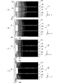
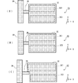
図2は、所定のバイアス電圧と大電力のRF信号が印加された状態での可動梁の変形量を示すコンター図である。図2(A),図2(B)には本発明の実施例に係る可動梁13,23を示しており、図2(C),図2(D)には比較例に係る可動梁33,43を示している。なお、各図中、共通する部位には同一の符号を付している。
図2(A)~(D)に示す可動梁13は,23,33,43において、可動部3Cが、駆動容量部形成領域3C1,3C2と、RF容量部形成領域3C3と、分割領域3Dとによって構成されている。RF容量部形成領域3C3は、可変容量部形成領域である。駆動容量部形成領域3C1,3C2と、RF容量部形成領域3C3と、分割領域3Dとは、それぞれX軸方向に長尺である。駆動容量部形成領域3C1とRF容量部形成領域3C3との間に分割領域3Dが配置されており、駆動容量部形成領域3C2とRF容量部形成領域3C3との間に分割領域3Dが配置されている。駆動容量部形成領域3C1,3C2は、アンカー部3A側(X軸負方向)の端部がRF容量部形成領域3C3よりも突出しており、突出部分に連結部3B1,3B2が接続されている。
図2(A)に示す可動梁13において、可動部3Cと連結部3B1,3B2との連結位置は、駆動容量部形成領域3C1,3C2の突出部分の内側側面(RF容量部形成領域3C3側の側面)である。この場合、可動部3Cの梁幅方向の撓みはあまり起こっていない。
図2(B)に示す可動梁23は,可動部3Cと連結部3B1,3B2との連結位置が可動梁13と相違する構成であり、可動部3Cと連結部3B1,3B2との連結位置は、アンカー部3A側(X軸負方向)の端部側面における、駆動容量部形成領域3C1,3C2の突出部分の内側側面(RF容量部形成領域3C3側の側面)の縁に重なる領域である。この場合にも、可動部3Cの梁幅方向の撓みはほとんど起こっていない。
図2(C),(D)に示す可動梁33,43も可動部3Cと連結部3B1,3B2との連結位置が可動梁13と相違する構成であり、可動部3Cと連結部3B1,3B2との連結位置は、駆動容量部形成領域3C1,3C2の外側側面(RF容量部形成領域3C3とは逆側の側面)である。この場合、可動部3Cの中央が大きく撓んでいる。
このように、大電力のRF信号が印加された状態では、可動部3Cと連結部3B1,3B2との連結位置の違いによって可動部3Cの梁幅方向での変形量が異なる。これは、セルフアクチエーションによる静電引力がRF容量部形成領域3C3に作用し、その静電引力の作用点と上記連結位置との距離によって、モーメント加重が変化するためと考えられる。したがって、本発明の実施例に係る可動梁13,23のように、セルフアクチエーションによる静電引力の作用点であるRF容量部形成領域3C3の近傍を上記連結位置とすることにより、RF容量部形成領域3C3に作用する静電引力による可動部3Cの梁幅方向の撓み量を抑制することができる。
《容量相関性》
次に、可変容量装置における駆動容量とRF容量との容量相関性について説明する。
次に、可変容量装置における駆動容量とRF容量との容量相関性について説明する。
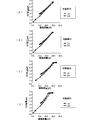
図3は図2に示した構成例ごとに駆動容量とRF容量との関係を説明するグラフであり、図4は図2に示した構成例の間での容量相関性に係る相関係数の差を説明するグラフである。
図3(A)~図3(D)のそれぞれには、RF信号を印加していない状態(DC=0V)と、大電力のRF信号を印加している状態(DC=20V)とでの駆動容量とRF容量との関係を示している。いずれの構成例でも、RF信号を印加していない状態よりも大電力のRF信号を印加している状態では、セルフアクチエーションの作用によってRF容量が増大している。
図4には、図3に示したグラフにおけるRF信号を印加していない状態(DC=0V)と、大電力のRF信号を印加している状態(DC=20V)とでの、容量相関性に係る相関係数を示している。RF信号を印加していない状態(DC=0V)では、本発明の実施例(可動梁13,23)でも比較例(可動梁33,43)でも、相関係数が略1.00であるが、大電力のRF信号を印加している状態(DC=20V)では、本発明の実施例(可動梁13,23)での相関係数が略1.00であるのに対して、比較例(可動梁33,43)での相関係数が大きく低下していることがわかる。
このように、比較例(可動梁33,43)ではセルフアクチエーションの影響によって相関係数が変動するのに対して、本発明の実施例(可動梁13,23)では相関係数がセルフアクチエーションの影響を殆ど受けず、容量相関性を安定したものにすることができる。このことから、本発明に係る可変容量装置では、RF容量の制御精度を高いものにすることが可能といえる。
《RF容量の最大値》
次に、可変容量装置におけるRF容量の最大値について説明する。
次に、可変容量装置におけるRF容量の最大値について説明する。
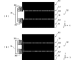
図5は可動梁の変形量を示すコンター図であり、具体的にはバイアス電圧を最大化した状態での可動梁の変形量を示している。図5(A)には本発明の実施例に係る可動梁53を示しており、図5(B)には比較例に係る可動梁63を示している。なお、各図中、共通する部位には同一の符号を付している。
可動梁53において、可動部3Cと連結部3B1,3B2との連結位置は、駆動容量部形成領域3C1,3C2の突出部分の内側側面(RF容量部形成領域3C3側の側面)である。可動梁63において、可動部3Cと連結部3B1,3B2との連結位置は、RF容量部形成領域3C3である。
バイアス電圧を最大化(DC=50V印加状態を図示)すると、可動梁53と可動梁63とにおける駆動容量部形成領域3C1,3C2が全長に亘って支持板2に近接した状態となり、RF容量部形成領域3C3における変形量とRF容量とが最大化する。この際、可動部3Cと連結部3B1,3B2との連結位置近傍は、完全に近接した状態にはならず、支持板2から浮き上がった状態となる。
このため、図5に示すように、可動梁53ではRF容量部形成領域3C3が全長に亘って支持板2に近接した状態に成るのに対して、可動梁63ではRF容量部形成領域3C3の一端近傍が支持板2から浮き上がった状態となる。
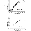
図6は、バイアス電圧とRF容量との関係、およびバイアス電圧と駆動容量との関係を説明するグラフである。図6において、Aは図5(A)に示す可動梁53であり、Bは図5(B)に示す可動梁63である。
図6に示すように、同じ値のバイアス電圧を印可した場合、本発明の実施例に係る可動梁53の方が比較例に係る可動梁63よりもRF容量が大きくなっている。可動梁53のようにRF容量部形成領域3C3が全長に亘って支持板2に近接した状態になれば、可変容量装置として実現可能なRF容量の最大値が大きくなる。一方、可動梁63のようにRF容量部形成領域3C3の一端近傍が支持板2から浮き上がった状態になれば、可変容量装置として実現可能なRF容量の最大値が小さくなってしまう。
このことから、本発明に係る可変容量装置では、梁幅方向を視て、連結部3B1,3B2が駆動容量部C2A,C2BのRF容量部C1A,C1B側の端部に重なる位置、または、駆動容量部C2A,C2BのRF容量部C1A,C1B側の端部よりもRF容量部C1A,C1B側でRF容量部C1A,C1Bから外れた位置で可動部3Cに連結されることにより、駆動容量とRF容量との容量相関性を高めたまま、RF容量の最大値を大きくすることが可能といえる。
《その他の実施例》
図7は、本発明の他の実施例に係る可変容量装置の可動梁の構成を説明する概略図である。
図7は、本発明の他の実施例に係る可変容量装置の可動梁の構成を説明する概略図である。
図7(A)~(C)に示す可動梁73,83,93は、1つの連結部3Bによってアンカー部3Aと可動部3Cとを連結する構成である。可動部3Cは、1つの駆動容量部形成領域3C1と、1つのRF容量部形成領域3C3とを備える。図7(A)に示す可動梁73において、可動部3Cと連結部3Bとの連結位置は、駆動容量部形成領域3C1のRF容量部形成領域3C3側の辺縁に重なる位置である。この構成では、RF容量の最大値が低減する可能性は残るが、少なくとも駆動容量とRF容量との容量相関性を高めることができる。
図7(B)に示す可動梁83は、上記可動梁73とは可動部3Cと連結部3Bとの連結位置が相違しており、駆動容量部形成領域3C1とRF容量部形成領域3C3との間の間隙に重なる位置である。この構成では、上記可動梁73よりもRF容量の最大値を高めることが可能である。
図7(C)に示す可動梁93は、上記可動梁73とは可動部3Cの形状が相違しており、可動部3Cにおける駆動容量部形成領域3C1がRF容量部形成領域3C3よりも連結部3B側に突出する構成である。そして、可動部3Cと連結部3Bとの連結位置が、突出する駆動容量部形成領域3C1の側壁面である。この構成では、上記可動梁83よりもRF容量の最大値をさらに高めることが可能である。
次に、通信装置のアンテナに接続されてインピーダンスマッチングに用いられるVMD(Variable Matching Device)装置について説明する。
図8(A)は、VMD装置111の等価回路図である。VMD装置111は、可変容量装置アレイ100と、インダクタLとを備える。可変容量装置アレイ100は、可変容量装置101A,101Bを備える。可変容量装置101Aは、外部負荷112AとインダクタLとの間を接続する信号ラインとグランドとの間に接続されている。可変容量装置101Bは、アンテナ112BとインダクタLとの間を接続する信号ラインとグランドとの間に接続されている。可変容量装置101A,101Bは、インダクタLを介して互いに接続されている。インダクタLの両端に、外部負荷112Aとアンテナ112Bとが接続されている。VMD装置111では、可変容量装置101A,101BのRF容量を制御することにより、外部負荷112Aとアンテナ112Bとのインピーダンスをマッチングさせることができる。
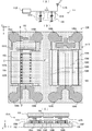
図8(B)、図8(C)は、可変容量装置アレイ100の構成を説明する図である。具体的には、図8(B)は、可変容量装置アレイ100の平面図(X-Y面平面図)である。図8(C)は、図8(B)中にC-C’で示す位置での可変容量装置アレイ100の断面図(Y-Z面断面図)である。ここで可変容量装置アレイ100は2組の可変容量装置101A,101Bを単一の支持板102に設けたパッケージ構成のものである。なお、図中、可変容量装置101Bは可動梁の図示を省いている。
可変容量装置101A,101Bはそれぞれ、可動梁103と、支持板側RF容量電極104A,104Bと、支持板側駆動容量電極105A,105Bと、可動梁側RF容量電極106と、可動梁側駆動容量電極107A,107Bと、誘電体膜108A~108Eと、同電位電極109とを備える。
可変容量装置101A,101Bにおいて、可動梁103は、本発明の特徴を持つ構成であり、連結部と可動部との連結位置がRF容量部形成領域の近傍である。支持板側RF容量電極104A,104Bと可動梁側RF容量電極106とは、対向する誘電体膜108CとともにRF容量部を構成する。支持板側駆動容量電極105A,105Bと可動梁側駆動容量電極107A,107Bとは、対向する誘電体膜108B,108Dとともに駆動容量部を構成する。同電位電極109は、可動梁側駆動容量電極107A,107Bに対向するように、支持板側駆動容量電極105A,105Bの両脇に設けられ、可動梁側駆動容量電極107A,107Bと同電位にされる。誘電体膜108A,108C,108Eは、誘電体膜108B,108Dが可動梁側駆動容量電極107A,107Bと間隔を隔てて対向するように、部分的に厚く構成されている。可変容量装置101A,101Bにおいては、同電位電極109を設けるとともに、誘電体膜108B,108Dが可動梁側駆動容量電極107A,107Bと接触しないようにすることで、バイアス電圧によって誘電体膜108B,108Dが帯電することを防いでいる。
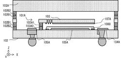
図9は、可変容量装置アレイ100のパッケージ構造(WaferLevel ChipSize Package)を説明する図である。具体的には、図9は、図8(B)中にD-D’で示す位置での可変容量装置アレイ100の断面図(X-Z面断面図)である。ここでは、ガラス基板からなる支持板102と高抵抗シリコン基板からなる可動梁103との間を、Auからなるアンカー部103A1,103A2の熱圧着により接合している。また、可変容量装置アレイ100は、ガラス基板からなるパッケージ蓋板102Aを備え、パッケージ蓋板102Aと支持板102との間を、Auからなる支持部材102B1,102B2の熱圧着により接合している。
このような構成により、パッケージ内部空間を減圧雰囲気に保持できるとともに、可動梁103側から支持板102に引き回す電極の抵抗を、Au-Au接合を介することによって、低くすることができる。なお、支持板102とパッケージ蓋板102Aとは、シリコン基板からなるものであってもよく、その場合、1kΩcm以上の抵抗率を持つことが好ましい。
以上のような各種構成であっても本発明は実施できる。RF容量部形成領域の近傍を可動部と連結部との連結位置とすることにより、セルフアクチエーションによりRF容量部形成領域に作用する静電引力の変動による、可動部の梁幅方向の撓みを抑制して、駆動容量とRF容量との容量相関性を改善することができる。
なお、上述の各実施形態では可動梁として片持ち梁構成のものを説明したが、本発明は両持ち梁構成の可動梁に対しても同様に実施することができる。また、可動梁を絶縁性のものとして、別途電極を形成して駆動容量部とRF容量部とを構成する構成を示したが、導電性の可動梁に対しても同様に実施することができる。その他、多様な構成で本発明は実施でき、本発明の範囲は上述の実施形態の記載に制限されるものではない。本発明の範囲は特許請求の範囲によって示され、特許請求の範囲と均等の意味および範囲内でのすべての変更が含まれることが意図される。
C1A,C1B…RF容量部
C2A,C2B…駆動容量部
1,101A,101B…可変容量装置
2,102…支持板
3,13,23,33,43,53,63,73,83,93,103…可動梁
3A…アンカー部
3B,3B1,3B2…連結部
3C…可動部
3C1,3C2…駆動容量部形成領域
3C3…RF容量部形成領域
3D…分割領域
4A,4B…支持板側RF容量電極
5A,5B…支持板側駆動容量電極
6…可動梁側RF容量電極
7A,7B…可動梁側駆動容量電極
8…誘電体膜
100…可変容量装置アレイ
C2A,C2B…駆動容量部
1,101A,101B…可変容量装置
2,102…支持板
3,13,23,33,43,53,63,73,83,93,103…可動梁
3A…アンカー部
3B,3B1,3B2…連結部
3C…可動部
3C1,3C2…駆動容量部形成領域
3C3…RF容量部形成領域
3D…分割領域
4A,4B…支持板側RF容量電極
5A,5B…支持板側駆動容量電極
6…可動梁側RF容量電極
7A,7B…可動梁側駆動容量電極
8…誘電体膜
100…可変容量装置アレイ
Claims (4)
- 支持板と、
前記支持板に対向して支持される可動部と、前記支持板に固定されるアンカー部と、前記アンカー部と前記可動部とを連結する連結部とを備える可動梁と、
前記可動部と前記支持板との対向領域に、前記支持板に近接するように前記可動部を変形させる静電力を生じさせる駆動容量部と、
前記可動部と前記支持板との対向領域に、前記可動部と前記支持板とが近接する状態に応じて容量の大きさが変化する可変容量部と、を備え、
前記駆動容量部と前記可変容量部とは、前記可動梁の梁幅方向に隣接するように配置され、
前記連結部は、前記駆動容量部の前記可変容量部側の端部に重なる位置、または、前記端部よりも前記可変容量部側の位置で前記可動部に連結される、可変容量装置。 - 前記連結部は、前記駆動容量部の前記可変容量部側の端部に重なる位置に連結される、請求項1に記載の可変容量装置。
- 前記可動部は、前記駆動容量部の配置領域が前記アンカー部側に突出する、請求項2に記載の可変容量装置。
- 前記連結部は前記駆動容量部の配置領域の前記可変容量部側を向く側面に連結される、請求項3に記載の可変容量装置。
Applications Claiming Priority (2)
| Application Number | Priority Date | Filing Date | Title |
|---|---|---|---|
| JP2010242905 | 2010-10-29 | ||
| JP2010-242905 | 2010-10-29 |
Publications (1)
| Publication Number | Publication Date |
|---|---|
| WO2012056889A1 true WO2012056889A1 (ja) | 2012-05-03 |
Family
ID=45993614
Family Applications (1)
| Application Number | Title | Priority Date | Filing Date |
|---|---|---|---|
| PCT/JP2011/073491 Ceased WO2012056889A1 (ja) | 2010-10-29 | 2011-10-13 | 可変容量装置 |
Country Status (1)
| Country | Link |
|---|---|
| WO (1) | WO2012056889A1 (ja) |
Citations (2)
| Publication number | Priority date | Publication date | Assignee | Title |
|---|---|---|---|---|
| JPH09153436A (ja) * | 1995-11-30 | 1997-06-10 | Murata Mfg Co Ltd | 可変容量コンデンサ |
| JP2003124063A (ja) * | 2001-10-18 | 2003-04-25 | Sony Corp | 容量可変型キャパシタ装置 |
-
2011
- 2011-10-13 WO PCT/JP2011/073491 patent/WO2012056889A1/ja not_active Ceased
Patent Citations (2)
| Publication number | Priority date | Publication date | Assignee | Title |
|---|---|---|---|---|
| JPH09153436A (ja) * | 1995-11-30 | 1997-06-10 | Murata Mfg Co Ltd | 可変容量コンデンサ |
| JP2003124063A (ja) * | 2001-10-18 | 2003-04-25 | Sony Corp | 容量可変型キャパシタ装置 |
Similar Documents
| Publication | Publication Date | Title |
|---|---|---|
| US7545081B2 (en) | Piezoelectric RF MEMS device and method of fabricating the same | |
| CN101093966B (zh) | 压电驱动mems装置 | |
| JP4580826B2 (ja) | マイクロメカニカルデバイス、マイクロスイッチ、容量可変キャパシタ、高周波回路及び光学スイッチ | |
| US8879132B2 (en) | Mirror driving apparatus, method of driving same and method of manufacturing same | |
| US7471031B2 (en) | Piezoelectric MEMS element and tunable filter equipped with the piezoelectric MEMS element | |
| US8847466B2 (en) | Piezoelectric bimorph switch | |
| KR101457462B1 (ko) | 진동 발전 디바이스 | |
| US7719169B2 (en) | Micro-electromechanical device | |
| JP2007273800A (ja) | 圧電駆動型memsアクチュエータ | |
| EP1385189A2 (en) | Switch | |
| US7830068B2 (en) | Actuator and electronic hardware using the same | |
| US7728703B2 (en) | RF MEMS switch and method for fabricating the same | |
| JP2013232536A (ja) | 可変容量デバイス及びその駆動方法 | |
| JP2009055683A (ja) | 圧電駆動型mems装置および携帯端末 | |
| WO2012056889A1 (ja) | 可変容量装置 | |
| JPH10149950A (ja) | 可変容量コンデンサ | |
| WO2012066901A1 (ja) | 可変容量装置 | |
| JP2008091167A (ja) | マイクロメカニカルデバイス | |
| US10508025B2 (en) | MEMS switch and electronic device | |
| JP2013042024A (ja) | 可変容量装置 | |
| JP2007259669A (ja) | 圧電アクチュエータ及びそれを用いたマイクロメカニカルデバイス、可変容量キャパシタ、スイッチ | |
| US7786830B2 (en) | Switch with movable portion | |
| JP6551071B2 (ja) | Memsスイッチ | |
| JP2007522609A (ja) | ピエゾ電気材料でできたマイクロ電気機械スイッチを備える電子装置 | |
| KR101368016B1 (ko) | 멤즈 스위치 |
Legal Events
| Date | Code | Title | Description |
|---|---|---|---|
| 121 | Ep: the epo has been informed by wipo that ep was designated in this application |
Ref document number: 11836028 Country of ref document: EP Kind code of ref document: A1 |
|
| NENP | Non-entry into the national phase |
Ref country code: DE |
|
| 122 | Ep: pct application non-entry in european phase |
Ref document number: 11836028 Country of ref document: EP Kind code of ref document: A1 |
|
| NENP | Non-entry into the national phase |
Ref country code: JP |