WO2012046603A1 - Light receiving element, optical sensor device, and method for manufacturing light receiving element - Google Patents
Light receiving element, optical sensor device, and method for manufacturing light receiving element Download PDFInfo
- Publication number
- WO2012046603A1 WO2012046603A1 PCT/JP2011/072251 JP2011072251W WO2012046603A1 WO 2012046603 A1 WO2012046603 A1 WO 2012046603A1 JP 2011072251 W JP2011072251 W JP 2011072251W WO 2012046603 A1 WO2012046603 A1 WO 2012046603A1
- Authority
- WO
- WIPO (PCT)
- Prior art keywords
- layer
- light receiving
- mqw
- receiving element
- light
- Prior art date
Links
- 238000000034 method Methods 0.000 title claims description 35
- 238000004519 manufacturing process Methods 0.000 title claims description 24
- 230000003287 optical effect Effects 0.000 title claims description 11
- 230000035945 sensitivity Effects 0.000 claims abstract description 71
- 239000000758 substrate Substances 0.000 claims abstract description 57
- 239000004065 semiconductor Substances 0.000 claims abstract description 32
- 150000001875 compounds Chemical class 0.000 claims abstract description 26
- 229910052787 antimony Inorganic materials 0.000 claims description 4
- 229910052785 arsenic Inorganic materials 0.000 claims description 4
- 229910052733 gallium Inorganic materials 0.000 claims description 4
- 229910001218 Gallium arsenide Inorganic materials 0.000 claims description 3
- 229910052751 metal Inorganic materials 0.000 claims description 2
- 239000002184 metal Substances 0.000 claims description 2
- 238000000927 vapour-phase epitaxy Methods 0.000 claims 1
- 230000006866 deterioration Effects 0.000 abstract 1
- 229910000530 Gallium indium arsenide Inorganic materials 0.000 description 50
- 239000007789 gas Substances 0.000 description 46
- 238000009792 diffusion process Methods 0.000 description 24
- 125000002524 organometallic group Chemical group 0.000 description 22
- 238000009826 distribution Methods 0.000 description 18
- 239000012535 impurity Substances 0.000 description 18
- 239000002994 raw material Substances 0.000 description 17
- 239000010453 quartz Substances 0.000 description 16
- VYPSYNLAJGMNEJ-UHFFFAOYSA-N silicon dioxide Inorganic materials O=[Si]=O VYPSYNLAJGMNEJ-UHFFFAOYSA-N 0.000 description 16
- 230000000052 comparative effect Effects 0.000 description 14
- 238000002488 metal-organic chemical vapour deposition Methods 0.000 description 13
- 230000007423 decrease Effects 0.000 description 12
- 239000013078 crystal Substances 0.000 description 11
- 230000005283 ground state Effects 0.000 description 10
- 230000015572 biosynthetic process Effects 0.000 description 8
- 238000000354 decomposition reaction Methods 0.000 description 8
- 238000010586 diagram Methods 0.000 description 8
- 230000005684 electric field Effects 0.000 description 8
- 230000000694 effects Effects 0.000 description 7
- 230000007704 transition Effects 0.000 description 7
- IBEFSUTVZWZJEL-UHFFFAOYSA-N trimethylindium Chemical compound C[In](C)C IBEFSUTVZWZJEL-UHFFFAOYSA-N 0.000 description 7
- QTQRGDBFHFYIBH-UHFFFAOYSA-N tert-butylarsenic Chemical compound CC(C)(C)[As] QTQRGDBFHFYIBH-UHFFFAOYSA-N 0.000 description 6
- XYFCBTPGUUZFHI-UHFFFAOYSA-N Phosphine Chemical compound P XYFCBTPGUUZFHI-UHFFFAOYSA-N 0.000 description 5
- 238000006243 chemical reaction Methods 0.000 description 5
- 230000008034 disappearance Effects 0.000 description 5
- 238000012360 testing method Methods 0.000 description 5
- RGGPNXQUMRMPRA-UHFFFAOYSA-N triethylgallium Chemical compound CC[Ga](CC)CC RGGPNXQUMRMPRA-UHFFFAOYSA-N 0.000 description 5
- OKTJSMMVPCPJKN-UHFFFAOYSA-N Carbon Chemical compound [C] OKTJSMMVPCPJKN-UHFFFAOYSA-N 0.000 description 4
- QVGXLLKOCUKJST-UHFFFAOYSA-N atomic oxygen Chemical compound [O] QVGXLLKOCUKJST-UHFFFAOYSA-N 0.000 description 4
- 229910052799 carbon Inorganic materials 0.000 description 4
- 230000008859 change Effects 0.000 description 4
- 238000001816 cooling Methods 0.000 description 4
- 238000000151 deposition Methods 0.000 description 4
- 230000008021 deposition Effects 0.000 description 4
- 238000005259 measurement Methods 0.000 description 4
- 239000001301 oxygen Substances 0.000 description 4
- 229910052760 oxygen Inorganic materials 0.000 description 4
- 239000000126 substance Substances 0.000 description 4
- ZGNPLWZYVAFUNZ-UHFFFAOYSA-N tert-butylphosphane Chemical compound CC(C)(C)P ZGNPLWZYVAFUNZ-UHFFFAOYSA-N 0.000 description 4
- IJGRMHOSHXDMSA-UHFFFAOYSA-N Atomic nitrogen Chemical compound N#N IJGRMHOSHXDMSA-UHFFFAOYSA-N 0.000 description 3
- 230000005281 excited state Effects 0.000 description 3
- 230000001681 protective effect Effects 0.000 description 3
- 229910052814 silicon oxide Inorganic materials 0.000 description 3
- OAICVXFJPJFONN-UHFFFAOYSA-N Phosphorus Chemical compound [P] OAICVXFJPJFONN-UHFFFAOYSA-N 0.000 description 2
- 238000010521 absorption reaction Methods 0.000 description 2
- 239000012159 carrier gas Substances 0.000 description 2
- 230000003247 decreasing effect Effects 0.000 description 2
- 238000010438 heat treatment Methods 0.000 description 2
- 238000003384 imaging method Methods 0.000 description 2
- 238000007689 inspection Methods 0.000 description 2
- 238000012423 maintenance Methods 0.000 description 2
- 239000000463 material Substances 0.000 description 2
- 229910052698 phosphorus Inorganic materials 0.000 description 2
- 239000011574 phosphorus Substances 0.000 description 2
- 229910000073 phosphorus hydride Inorganic materials 0.000 description 2
- 238000005036 potential barrier Methods 0.000 description 2
- 238000002360 preparation method Methods 0.000 description 2
- 230000009467 reduction Effects 0.000 description 2
- 238000010183 spectrum analysis Methods 0.000 description 2
- VCZQFJFZMMALHB-UHFFFAOYSA-N tetraethylsilane Chemical compound CC[Si](CC)(CC)CC VCZQFJFZMMALHB-UHFFFAOYSA-N 0.000 description 2
- OTRPZROOJRIMKW-UHFFFAOYSA-N triethylindigane Chemical compound CC[In](CC)CC OTRPZROOJRIMKW-UHFFFAOYSA-N 0.000 description 2
- HTDIUWINAKAPER-UHFFFAOYSA-N trimethylarsine Chemical compound C[As](C)C HTDIUWINAKAPER-UHFFFAOYSA-N 0.000 description 2
- XCZXGTMEAKBVPV-UHFFFAOYSA-N trimethylgallium Chemical compound C[Ga](C)C XCZXGTMEAKBVPV-UHFFFAOYSA-N 0.000 description 2
- PORFVJURJXKREL-UHFFFAOYSA-N trimethylstibine Chemical compound C[Sb](C)C PORFVJURJXKREL-UHFFFAOYSA-N 0.000 description 2
- GYHNNYVSQQEPJS-UHFFFAOYSA-N Gallium Chemical compound [Ga] GYHNNYVSQQEPJS-UHFFFAOYSA-N 0.000 description 1
- 241001465754 Metazoa Species 0.000 description 1
- 238000000862 absorption spectrum Methods 0.000 description 1
- WATWJIUSRGPENY-UHFFFAOYSA-N antimony atom Chemical compound [Sb] WATWJIUSRGPENY-UHFFFAOYSA-N 0.000 description 1
- 238000013459 approach Methods 0.000 description 1
- RQNWIZPPADIBDY-UHFFFAOYSA-N arsenic atom Chemical compound [As] RQNWIZPPADIBDY-UHFFFAOYSA-N 0.000 description 1
- 230000004888 barrier function Effects 0.000 description 1
- 230000009286 beneficial effect Effects 0.000 description 1
- 230000000593 degrading effect Effects 0.000 description 1
- 238000001514 detection method Methods 0.000 description 1
- 238000005516 engineering process Methods 0.000 description 1
- 230000007613 environmental effect Effects 0.000 description 1
- 238000011156 evaluation Methods 0.000 description 1
- 230000005284 excitation Effects 0.000 description 1
- 239000003574 free electron Substances 0.000 description 1
- 125000005842 heteroatom Chemical group 0.000 description 1
- 239000001257 hydrogen Substances 0.000 description 1
- 229910052739 hydrogen Inorganic materials 0.000 description 1
- 125000004435 hydrogen atom Chemical class [H]* 0.000 description 1
- 230000001771 impaired effect Effects 0.000 description 1
- 230000006872 improvement Effects 0.000 description 1
- 229910052738 indium Inorganic materials 0.000 description 1
- APFVFJFRJDLVQX-UHFFFAOYSA-N indium atom Chemical compound [In] APFVFJFRJDLVQX-UHFFFAOYSA-N 0.000 description 1
- 230000010365 information processing Effects 0.000 description 1
- 239000013067 intermediate product Substances 0.000 description 1
- 230000031700 light absorption Effects 0.000 description 1
- 239000007788 liquid Substances 0.000 description 1
- 238000012986 modification Methods 0.000 description 1
- 230000004048 modification Effects 0.000 description 1
- 238000012806 monitoring device Methods 0.000 description 1
- 238000012544 monitoring process Methods 0.000 description 1
- 229910052757 nitrogen Inorganic materials 0.000 description 1
- 230000002093 peripheral effect Effects 0.000 description 1
- 238000005191 phase separation Methods 0.000 description 1
- 238000005424 photoluminescence Methods 0.000 description 1
- 230000008569 process Effects 0.000 description 1
- 238000001953 recrystallisation Methods 0.000 description 1
- 230000004043 responsiveness Effects 0.000 description 1
- 238000001004 secondary ion mass spectrometry Methods 0.000 description 1
- 238000004904 shortening Methods 0.000 description 1
- 238000009751 slip forming Methods 0.000 description 1
- 239000007787 solid Substances 0.000 description 1
- 238000002798 spectrophotometry method Methods 0.000 description 1
- RBEXEKTWBGMBDZ-UHFFFAOYSA-N tri(propan-2-yl)stibane Chemical compound CC(C)[Sb](C(C)C)C(C)C RBEXEKTWBGMBDZ-UHFFFAOYSA-N 0.000 description 1
- VLCQZHSMCYCDJL-UHFFFAOYSA-N tribenuron methyl Chemical compound COC(=O)C1=CC=CC=C1S(=O)(=O)NC(=O)N(C)C1=NC(C)=NC(OC)=N1 VLCQZHSMCYCDJL-UHFFFAOYSA-N 0.000 description 1
- KKOFCVMVBJXDFP-UHFFFAOYSA-N triethylstibane Chemical compound CC[Sb](CC)CC KKOFCVMVBJXDFP-UHFFFAOYSA-N 0.000 description 1
- 238000001947 vapour-phase growth Methods 0.000 description 1
- 238000012795 verification Methods 0.000 description 1
- XLYOFNOQVPJJNP-UHFFFAOYSA-N water Substances O XLYOFNOQVPJJNP-UHFFFAOYSA-N 0.000 description 1
Images


Classifications
-
- H—ELECTRICITY
- H01—ELECTRIC ELEMENTS
- H01L—SEMICONDUCTOR DEVICES NOT COVERED BY CLASS H10
- H01L31/00—Semiconductor devices sensitive to infrared radiation, light, electromagnetic radiation of shorter wavelength or corpuscular radiation and specially adapted either for the conversion of the energy of such radiation into electrical energy or for the control of electrical energy by such radiation; Processes or apparatus specially adapted for the manufacture or treatment thereof or of parts thereof; Details thereof
- H01L31/0248—Semiconductor devices sensitive to infrared radiation, light, electromagnetic radiation of shorter wavelength or corpuscular radiation and specially adapted either for the conversion of the energy of such radiation into electrical energy or for the control of electrical energy by such radiation; Processes or apparatus specially adapted for the manufacture or treatment thereof or of parts thereof; Details thereof characterised by their semiconductor bodies
- H01L31/0352—Semiconductor devices sensitive to infrared radiation, light, electromagnetic radiation of shorter wavelength or corpuscular radiation and specially adapted either for the conversion of the energy of such radiation into electrical energy or for the control of electrical energy by such radiation; Processes or apparatus specially adapted for the manufacture or treatment thereof or of parts thereof; Details thereof characterised by their semiconductor bodies characterised by their shape or by the shapes, relative sizes or disposition of the semiconductor regions
- H01L31/035236—Superlattices; Multiple quantum well structures
-
- H—ELECTRICITY
- H01—ELECTRIC ELEMENTS
- H01L—SEMICONDUCTOR DEVICES NOT COVERED BY CLASS H10
- H01L31/00—Semiconductor devices sensitive to infrared radiation, light, electromagnetic radiation of shorter wavelength or corpuscular radiation and specially adapted either for the conversion of the energy of such radiation into electrical energy or for the control of electrical energy by such radiation; Processes or apparatus specially adapted for the manufacture or treatment thereof or of parts thereof; Details thereof
- H01L31/08—Semiconductor devices sensitive to infrared radiation, light, electromagnetic radiation of shorter wavelength or corpuscular radiation and specially adapted either for the conversion of the energy of such radiation into electrical energy or for the control of electrical energy by such radiation; Processes or apparatus specially adapted for the manufacture or treatment thereof or of parts thereof; Details thereof in which radiation controls flow of current through the device, e.g. photoresistors
- H01L31/10—Semiconductor devices sensitive to infrared radiation, light, electromagnetic radiation of shorter wavelength or corpuscular radiation and specially adapted either for the conversion of the energy of such radiation into electrical energy or for the control of electrical energy by such radiation; Processes or apparatus specially adapted for the manufacture or treatment thereof or of parts thereof; Details thereof in which radiation controls flow of current through the device, e.g. photoresistors characterised by at least one potential-jump barrier or surface barrier, e.g. phototransistors
-
- B—PERFORMING OPERATIONS; TRANSPORTING
- B82—NANOTECHNOLOGY
- B82Y—SPECIFIC USES OR APPLICATIONS OF NANOSTRUCTURES; MEASUREMENT OR ANALYSIS OF NANOSTRUCTURES; MANUFACTURE OR TREATMENT OF NANOSTRUCTURES
- B82Y20/00—Nanooptics, e.g. quantum optics or photonic crystals
-
- H—ELECTRICITY
- H01—ELECTRIC ELEMENTS
- H01L—SEMICONDUCTOR DEVICES NOT COVERED BY CLASS H10
- H01L27/00—Devices consisting of a plurality of semiconductor or other solid-state components formed in or on a common substrate
- H01L27/14—Devices consisting of a plurality of semiconductor or other solid-state components formed in or on a common substrate including semiconductor components sensitive to infrared radiation, light, electromagnetic radiation of shorter wavelength or corpuscular radiation and specially adapted either for the conversion of the energy of such radiation into electrical energy or for the control of electrical energy by such radiation
- H01L27/144—Devices controlled by radiation
- H01L27/146—Imager structures
- H01L27/14601—Structural or functional details thereof
- H01L27/1464—Back illuminated imager structures
-
- H—ELECTRICITY
- H01—ELECTRIC ELEMENTS
- H01L—SEMICONDUCTOR DEVICES NOT COVERED BY CLASS H10
- H01L31/00—Semiconductor devices sensitive to infrared radiation, light, electromagnetic radiation of shorter wavelength or corpuscular radiation and specially adapted either for the conversion of the energy of such radiation into electrical energy or for the control of electrical energy by such radiation; Processes or apparatus specially adapted for the manufacture or treatment thereof or of parts thereof; Details thereof
- H01L31/08—Semiconductor devices sensitive to infrared radiation, light, electromagnetic radiation of shorter wavelength or corpuscular radiation and specially adapted either for the conversion of the energy of such radiation into electrical energy or for the control of electrical energy by such radiation; Processes or apparatus specially adapted for the manufacture or treatment thereof or of parts thereof; Details thereof in which radiation controls flow of current through the device, e.g. photoresistors
- H01L31/10—Semiconductor devices sensitive to infrared radiation, light, electromagnetic radiation of shorter wavelength or corpuscular radiation and specially adapted either for the conversion of the energy of such radiation into electrical energy or for the control of electrical energy by such radiation; Processes or apparatus specially adapted for the manufacture or treatment thereof or of parts thereof; Details thereof in which radiation controls flow of current through the device, e.g. photoresistors characterised by at least one potential-jump barrier or surface barrier, e.g. phototransistors
- H01L31/101—Devices sensitive to infrared, visible or ultraviolet radiation
- H01L31/102—Devices sensitive to infrared, visible or ultraviolet radiation characterised by only one potential barrier or surface barrier
- H01L31/105—Devices sensitive to infrared, visible or ultraviolet radiation characterised by only one potential barrier or surface barrier the potential barrier being of the PIN type
-
- H—ELECTRICITY
- H01—ELECTRIC ELEMENTS
- H01L—SEMICONDUCTOR DEVICES NOT COVERED BY CLASS H10
- H01L31/00—Semiconductor devices sensitive to infrared radiation, light, electromagnetic radiation of shorter wavelength or corpuscular radiation and specially adapted either for the conversion of the energy of such radiation into electrical energy or for the control of electrical energy by such radiation; Processes or apparatus specially adapted for the manufacture or treatment thereof or of parts thereof; Details thereof
- H01L31/18—Processes or apparatus specially adapted for the manufacture or treatment of these devices or of parts thereof
- H01L31/184—Processes or apparatus specially adapted for the manufacture or treatment of these devices or of parts thereof the active layers comprising only AIIIBV compounds, e.g. GaAs, InP
- H01L31/1844—Processes or apparatus specially adapted for the manufacture or treatment of these devices or of parts thereof the active layers comprising only AIIIBV compounds, e.g. GaAs, InP comprising ternary or quaternary compounds, e.g. Ga Al As, In Ga As P
-
- H—ELECTRICITY
- H01—ELECTRIC ELEMENTS
- H01L—SEMICONDUCTOR DEVICES NOT COVERED BY CLASS H10
- H01L31/00—Semiconductor devices sensitive to infrared radiation, light, electromagnetic radiation of shorter wavelength or corpuscular radiation and specially adapted either for the conversion of the energy of such radiation into electrical energy or for the control of electrical energy by such radiation; Processes or apparatus specially adapted for the manufacture or treatment thereof or of parts thereof; Details thereof
- H01L31/18—Processes or apparatus specially adapted for the manufacture or treatment of these devices or of parts thereof
- H01L31/184—Processes or apparatus specially adapted for the manufacture or treatment of these devices or of parts thereof the active layers comprising only AIIIBV compounds, e.g. GaAs, InP
- H01L31/1852—Processes or apparatus specially adapted for the manufacture or treatment of these devices or of parts thereof the active layers comprising only AIIIBV compounds, e.g. GaAs, InP comprising a growth substrate not being an AIIIBV compound
-
- H—ELECTRICITY
- H01—ELECTRIC ELEMENTS
- H01L—SEMICONDUCTOR DEVICES NOT COVERED BY CLASS H10
- H01L27/00—Devices consisting of a plurality of semiconductor or other solid-state components formed in or on a common substrate
- H01L27/14—Devices consisting of a plurality of semiconductor or other solid-state components formed in or on a common substrate including semiconductor components sensitive to infrared radiation, light, electromagnetic radiation of shorter wavelength or corpuscular radiation and specially adapted either for the conversion of the energy of such radiation into electrical energy or for the control of electrical energy by such radiation
- H01L27/144—Devices controlled by radiation
- H01L27/146—Imager structures
- H01L27/14601—Structural or functional details thereof
- H01L27/14634—Assemblies, i.e. Hybrid structures
-
- H—ELECTRICITY
- H01—ELECTRIC ELEMENTS
- H01L—SEMICONDUCTOR DEVICES NOT COVERED BY CLASS H10
- H01L27/00—Devices consisting of a plurality of semiconductor or other solid-state components formed in or on a common substrate
- H01L27/14—Devices consisting of a plurality of semiconductor or other solid-state components formed in or on a common substrate including semiconductor components sensitive to infrared radiation, light, electromagnetic radiation of shorter wavelength or corpuscular radiation and specially adapted either for the conversion of the energy of such radiation into electrical energy or for the control of electrical energy by such radiation
- H01L27/144—Devices controlled by radiation
- H01L27/146—Imager structures
- H01L27/14601—Structural or functional details thereof
- H01L27/14636—Interconnect structures
-
- H—ELECTRICITY
- H01—ELECTRIC ELEMENTS
- H01L—SEMICONDUCTOR DEVICES NOT COVERED BY CLASS H10
- H01L27/00—Devices consisting of a plurality of semiconductor or other solid-state components formed in or on a common substrate
- H01L27/14—Devices consisting of a plurality of semiconductor or other solid-state components formed in or on a common substrate including semiconductor components sensitive to infrared radiation, light, electromagnetic radiation of shorter wavelength or corpuscular radiation and specially adapted either for the conversion of the energy of such radiation into electrical energy or for the control of electrical energy by such radiation
- H01L27/144—Devices controlled by radiation
- H01L27/146—Imager structures
- H01L27/14643—Photodiode arrays; MOS imagers
- H01L27/14645—Colour imagers
- H01L27/14647—Multicolour imagers having a stacked pixel-element structure, e.g. npn, npnpn or MQW elements
-
- H—ELECTRICITY
- H01—ELECTRIC ELEMENTS
- H01L—SEMICONDUCTOR DEVICES NOT COVERED BY CLASS H10
- H01L27/00—Devices consisting of a plurality of semiconductor or other solid-state components formed in or on a common substrate
- H01L27/14—Devices consisting of a plurality of semiconductor or other solid-state components formed in or on a common substrate including semiconductor components sensitive to infrared radiation, light, electromagnetic radiation of shorter wavelength or corpuscular radiation and specially adapted either for the conversion of the energy of such radiation into electrical energy or for the control of electrical energy by such radiation
- H01L27/144—Devices controlled by radiation
- H01L27/146—Imager structures
- H01L27/14643—Photodiode arrays; MOS imagers
- H01L27/14649—Infrared imagers
- H01L27/14652—Multispectral infrared imagers, having a stacked pixel-element structure, e.g. npn, npnpn or MQW structures
-
- H—ELECTRICITY
- H01—ELECTRIC ELEMENTS
- H01L—SEMICONDUCTOR DEVICES NOT COVERED BY CLASS H10
- H01L29/00—Semiconductor devices adapted for rectifying, amplifying, oscillating or switching, or capacitors or resistors with at least one potential-jump barrier or surface barrier, e.g. PN junction depletion layer or carrier concentration layer; Details of semiconductor bodies or of electrodes thereof ; Multistep manufacturing processes therefor
- H01L29/02—Semiconductor bodies ; Multistep manufacturing processes therefor
- H01L29/12—Semiconductor bodies ; Multistep manufacturing processes therefor characterised by the materials of which they are formed
- H01L29/15—Structures with periodic or quasi periodic potential variation, e.g. multiple quantum wells, superlattices
-
- Y—GENERAL TAGGING OF NEW TECHNOLOGICAL DEVELOPMENTS; GENERAL TAGGING OF CROSS-SECTIONAL TECHNOLOGIES SPANNING OVER SEVERAL SECTIONS OF THE IPC; TECHNICAL SUBJECTS COVERED BY FORMER USPC CROSS-REFERENCE ART COLLECTIONS [XRACs] AND DIGESTS
- Y02—TECHNOLOGIES OR APPLICATIONS FOR MITIGATION OR ADAPTATION AGAINST CLIMATE CHANGE
- Y02E—REDUCTION OF GREENHOUSE GAS [GHG] EMISSIONS, RELATED TO ENERGY GENERATION, TRANSMISSION OR DISTRIBUTION
- Y02E10/00—Energy generation through renewable energy sources
- Y02E10/50—Photovoltaic [PV] energy
- Y02E10/544—Solar cells from Group III-V materials
-
- Y—GENERAL TAGGING OF NEW TECHNOLOGICAL DEVELOPMENTS; GENERAL TAGGING OF CROSS-SECTIONAL TECHNOLOGIES SPANNING OVER SEVERAL SECTIONS OF THE IPC; TECHNICAL SUBJECTS COVERED BY FORMER USPC CROSS-REFERENCE ART COLLECTIONS [XRACs] AND DIGESTS
- Y02—TECHNOLOGIES OR APPLICATIONS FOR MITIGATION OR ADAPTATION AGAINST CLIMATE CHANGE
- Y02P—CLIMATE CHANGE MITIGATION TECHNOLOGIES IN THE PRODUCTION OR PROCESSING OF GOODS
- Y02P70/00—Climate change mitigation technologies in the production process for final industrial or consumer products
- Y02P70/50—Manufacturing or production processes characterised by the final manufactured product
Definitions
- the present invention relates to a III-V compound semiconductor light receiving element, an optical sensor device, and a method for manufacturing the light receiving element. More specifically, a light receiving element, an optical sensor device, and a type 2 multiple quantum well structure (MQW: Multiple-Quantum Well) having a light receiving sensitivity in the near-infrared long wavelength region are included in the light receiving layer.
- the present invention relates to a method for manufacturing a light receiving element.
- Non-Patent Document 1 discloses a photodiode having a light-receiving layer of InGaAs / GaAsSb type 2 MQW lattice-matched to an InP substrate of a III-V compound semiconductor.
- This MQW is composed of a repetition number of 150 (a number of pairs of 150) with InGaAs having a thickness of 5 nm and GaAsSb having a thickness of 5 nm as a pair.
- a cutoff wavelength of about 2.39 ⁇ m can be obtained.
- the light receiving element has a structure in which the cap layer on the opposite side to the InP substrate is a p-conductivity type with respect to the light-receiving layer, the InP substrate is an n-conductivity type, and light is incident from the back side of the InP substrate.
- Non-Patent Document 2 discloses the wavelength dependence of sensitivity for a photodiode having the same structure as described above. The sensitivity is not flat with respect to the wavelength but shows a strong wavelength dependence.
- the sensitivity of the photodiode having the MQW of type 2 InGaAs (thickness 5 nm) / GaAsSb (thickness 5 nm) is relatively high on the long wavelength side near the wavelength of 2.3 ⁇ m, but greatly decreases near the wavelength of 1.5 ⁇ m. This drop in sensitivity near the wavelength of 1.5 ⁇ m is not preferable in spectral analysis or the like.
- the sensitivity is preferably flat over the entire wavelength range. However, it is not preferable that the sensitivity is low stability, and it is preferable that the sensitivity be flat or fluctuate with respect to the wavelength while being above a predetermined level.
- the present invention relates to a light receiving element having an MQW of type 2 and capable of preventing a drop in sensitivity in a short wavelength range while improving the sensitivity over the entire wavelength range where light can be received. It is an object of the present invention to provide an optical sensor device and a method for manufacturing a light receiving element.
- the light receiving element may be an element having a single pixel, or may be an element arranged in a one-dimensional or two-dimensional array.
- the light-receiving element of the present invention is formed on a group III-V compound semiconductor substrate and has pixels.
- the light receiving element includes a type 2 MQW light receiving layer located on a substrate, and MQW includes two or more pairs of two different III-V compound semiconductor layers, and two different III- Among the group V compound semiconductor layers, the layer having the higher valence band potential is made thinner than the other layer.
- the electrons in the valence band are excited to the conduction band, and vacancies are generated in the valence band. That is, an electron / hole pair is formed by light reception.
- the electrons reach the n-side electrode and the vacancies reach the p-side electrode and need to be detected as charges or currents.
- One of the n-side electrode and the p-side electrode needs to be arranged for each pixel. Electrons move through the conduction band and reach the n-side electrode, and holes move through the valence band and reach the p-side electrode, whereby the charge or current is detected.
- the effective mass in the conduction band of electrons in a compound semiconductor is about 0.05 m (m: mass of free electrons), whereas the effective mass of holes in the valence band (heavy holes) Is large, for example, about 10 times or more of electrons.
- the phenomenon peculiar to the reception of the type 2 MQW is as follows. That is, in light reception on the long wavelength side in Type 2 MQW, holes are generated in a layer having a higher valence band (hereinafter referred to as a higher layer).
- the valence band of the adjacent layer (the layer with the lower valence band (hereinafter referred to as the lower layer)) forms a well-type barrier with respect to the valence band of the higher layer. For this reason, the holes generated by light reception have resistance to movement by the potential barrier formed by the adjacent lower layer in addition to the extremely large effective mass compared to the electrons as described above.
- In Type 2 MQW light reception on the long wavelength side occurs at the interface between the higher layer and the lower layer.
- Type 2 MQW is used to expand the light receiving sensitivity to the longer wavelength side.
- the sensitivity in the long wavelength region cannot be increased beyond the practical level.
- the number of pairs is 50 or more.
- the following two arrangement configurations (F1) and (F2) cover all arrangement configurations, but are classified for the purpose of organizing the concept.
- the present invention has a beneficial effect.
- (F1) When the incident surface and the p-side electrode are in a positional relationship such that the MQW is sandwiched between them, the light on the short wavelength side tends to be received at the MQW end near the incident surface. For this reason, of the generated holes / electrons, the holes cannot reach the p-side electrode unless they move through almost the entire thickness of the MQW. Holes are more likely to disappear during the movement of MQW, resulting in a decrease in sensitivity.
- the wavelength limit refers to a longer wavelength limit.
- the wavelength limit at which light can be received in type 2 MQW is determined by the difference between the ground state energy of the valence band of the higher layer and the ground state energy of the conduction band of the lower layer. Generally, when the thickness of the quantum well layer is reduced, the energy of the ground state for electrons increases greatly, but the increase of the energy of the ground state for holes is small. The reason is that the effective mass greatly affects the energy level of electrons or holes.
- the energy level is low and the ground state energy level is also low.
- Light reception is possible by reducing the thickness of the higher layer (holes are generated in its valence band) and the lower layer (electrons are generated in its conduction band) to a specified level or more.
- the critical wavelength limit hardly changes.
- high sensitivity can be maintained by setting MQW of 50 pairs or more. (E2) In a light reception standby state, a reverse bias voltage is applied between both electrodes to apply an electric field in the MQW. Holes and electrons move through the MQW driven by this electric field.
- the strength of the electric field generated in the MQW by a constant bias voltage can be increased.
- the disappearance of holes can be suppressed and the sensitivity can be increased.
- E3 The effect of suppressing the disappearance of holes is effective regardless of the wavelength of the received light.
- the film thickness of the layer having the higher valence band potential can be made 1 nm or more thinner than the film thickness of the other layer.
- the total thickness of the MQW can be reliably reduced while securing a predetermined number or more of pairs.
- the sensitivity can be increased in the entire wavelength region below the wavelength limit.
- (F1) it is possible to improve the sensitivity of light in a short wavelength range in which light reception is likely to occur at an end far from the p-side electrode.
- a cap layer located on the light receiving layer is provided, and the pixel region in the cap layer is of p conductivity type, and the back surface of the substrate can be a light incident surface.
- the p-side electrode is located on a p-conductivity type pixel. Holes generated by light reception tend to disappear while moving in the valence band toward the p-side electrode. As a result, sensitivity decreases. In particular, when light is received at the end of the MQW close to the substrate, the holes generated there do not contribute to sensitivity unless they move through almost the entire thickness of the MQW. As described above, in the present invention, the total thickness of MQW can be reduced without significantly affecting the wavelength limit of light reception.
- a cap layer located on the light receiving layer is provided, and the pixel region in the cap layer is of n conductivity type, and light can enter from the cap layer side.
- the p-side electrode is a ground electrode. Since the incident light is usually received as soon as it is incident, holes cannot contribute to sensitivity unless they move almost the total thickness of the MQW and reach the p-side electrode. In particular, light on the short wavelength side tends to be received immediately after entering the MQW, and therefore tends to not contribute to sensitivity. However, in the present invention, since the total thickness of the MQW is reduced without significantly affecting the wavelength limit of light reception and maintaining the sensitivity on the long wavelength side, the frequency of annihilation during the movement of the holes during MQW movement is reduced. , And sensitivity can be maintained. In particular, it is effective for preventing a decrease in sensitivity on the short wavelength side.
- the substrate can be an InP substrate.
- InP substrate As a result, it is possible to obtain a light receiving element having a sensitivity in the near infrared region and having a low dark current due to good crystallinity using an InP substrate that has been used for many years.
- the layer having the higher valence band potential can contain Ga, As, and Sb. This makes it possible to form a III-V group compound semiconductor layer such as GaAsSb, GaAsSbN, or GaAsSbP having a high valence band potential.
- a III-V group compound semiconductor layer such as GaAsSb, GaAsSbN, or GaAsSbP having a high valence band potential.
- an InP substrate since the lattice matching is good, a high-quality light receiving element with low dark current can be obtained.
- MQW is a type 2 MQW composed of a pair of In x Ga 1-x As (0.38 ⁇ x ⁇ 0.68) and GaAs y Sb 1-y (0.36 ⁇ y ⁇ 0.62) can do.
- a high-quality light-receiving element that can cover the wavelength limit of light reception that is 2.5 ⁇ m or more and close to 3 ⁇ m.
- the light receiving element can have a sensitivity to light having a wavelength of 1500 nm of 0.5 A / W or more. As a result, since the sensitivity on the short wavelength side is too small, information processing such as spectrum analysis is not hindered.
- a regrowth interface between the top surface of the MQW and the bottom surface of the cap layer. Since impurities such as oxygen and carbon are concentrated on the regrowth interface, the crystallinity of the epitaxial layer formed on the regrowth interface is deteriorated, resulting in an increase in dark current and the like. By not having a regrowth interface in the above portion, a good crystal layer can be obtained and dark current can be reduced.
- the optical sensor device of the present invention is characterized by using any of the light receiving elements described above.
- high-quality light-receiving elements that have sensitivity in the near-infrared region and low dark current can be used at room temperature in fields that have previously been impossible to sense without cooling devices, such as living organisms and the environment. And a small device can be provided. If a cooling device is required, power for that purpose or supply of liquid nitrogen or the like is required. For this reason, large restrictions are imposed in terms of size, cooling maintenance, and cost for cooling maintenance.
- the present invention enables highly accurate sensing for a field that has been impossible for such a reason.
- the method for manufacturing a light receiving element of the present invention manufactures a light receiving element formed on a substrate of a III-V compound semiconductor and having pixels.
- the manufacturing method includes a step of growing a type 2 MQW light-receiving layer on a substrate.
- the first layer and the second layer of a group III-V compound semiconductor are paired.
- the potential of the valence band of the first layer is higher than the potential of the valence band of the second layer, and in the MQW growth process, the thickness of the first layer is made thinner than the thickness of the second layer. , 50 or more pairs are stacked.
- the method further includes a step of forming a layer including a group III-V compound semiconductor.
- the step of forming MQW and the step of forming a layer including a group III-V compound semiconductor From the start of the growth of MQW to the end of the growth of the layer containing the III-V compound semiconductor, the same growth tank is formed by the all-organic vapor phase growth method (the all-organic MOVPE method) so as not to include the step of forming the growth interface. Can grow within. Thereby, a laminate having excellent crystallinity can be formed on the MQW.
- the semiconductor element or the like of the present invention it is possible to prevent a drop in sensitivity in a short wavelength range while improving sensitivity over the entire wavelength range where light can be received using type 2 MQW.
- FIG. 1 is an optical sensor device including a light receiving element of the present invention in which a plurality of pixels are arranged. It is a figure which shows the measurement result of PL peak wavelength (median value) of each test body in Example 1. It is a figure which shows the influence (measurement result) of the total film thickness of MQW and the wavelength which acts on the sensitivity R of each test body in Example 2.
- FIG. 1 shows the measurement result of PL peak wavelength (median value) of each test body in Example 1.
- FIG. 1 shows the influence (measurement result) of the total film thickness of MQW and the wavelength which acts on the sensitivity R of each test body in Example 2.
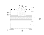
- InP substrate 2 buffer layer (InP and / or InGaAs), 3 type 2 MQW light-receiving layer, 3a layer with higher valence band potential (GaAsSb), 3b layer with lower valence band potential (InGaAs) 3u 1 pair, 4 InGaAs layer (diffusion concentration distribution adjustment layer), 5 InP cap layer, 6 p-type region, 10 optical sensor device (detection device), 11 p-side electrode (pixel electrode), 12 ground electrode (n-side) Electrode), 12b bump, 15 pn junction, 16 interface between MQW and InGaAs layer, 17 interface between InGaAs layer (diffusion concentration distribution adjusting layer) and InP window layer, 35 AR (antireflection) film, 36 selective diffusion mask pattern 39 Bond bump, 43 Protective film (Si N film), 50 light receiving element (light receiving element array), 50a wafer (intermediate product), 60, all organic MOVPE film forming device, 61, infrared temperature monitoring
- FIG. 1A is a diagram showing a light receiving element 50 according to an embodiment of the present invention.
- the light receiving element 50 has an InP semiconductor stacked structure (epitaxial wafer) of the following configuration on the InP substrate 1.
- InP semiconductor stacked structure epipitaxial wafer
- FIG. 1A light is incident from the back side of the InP substrate 1.
- it can also take the structure which injects from an epitaxial side.
- the p-type region 6 is positioned so as to reach the MQW light-receiving layer 3 from the surface of the InP cap layer 5.
- the p-type region 6 is formed by selective diffusion of p-type impurity Zn from the opening of the selective diffusion mask pattern 36 of the SiN film.
- Zn is diffused and introduced into the inner periphery of the peripheral portion of the light receiving element 50 in a plan view.
- a p-side electrode 11 made of AuZn is provided in the p-type region 6, and an n-side electrode 12 made of AuGeNi is provided in ohmic contact with the back surface of the InP substrate 1.
- the InP substrate 1 is doped with n-type impurities and has a predetermined level of conductivity. However, the InP substrate 1 may not have conductivity.
- the n-side electrode 12 is disposed so as to be in ohmic contact with the n-type InP buffer layer 2.
- An SiON antireflection film 35 is provided on the back surface of the InP substrate 1 so that light enters from the back surface side of the InP substrate. Accordingly, the light receiving element 50 shown in FIG. 1A corresponds to the arrangement configuration (F1).
- a pn junction 15 is formed at a position corresponding to the boundary front of the p-type region 6, and a reverse bias voltage is applied between the p-side electrode 11 and the n-side electrode 12.
- a depletion layer is formed more widely on the side where the n-type impurity concentration is low (n-type impurity background).
- the n-type impurity background in the MQW light-receiving layer 3 is about 5E15 (5 ⁇ 10 15 ) cm ⁇ 3 or less in terms of n-type impurity concentration (carrier concentration).
- the position 15 of the pn junction is determined by the intersection of the background (n-type carrier concentration) of the light-receiving layer 3 of the multiple quantum well and the concentration profile of the p-type impurity Zn.
- the InGaAs diffusion concentration distribution adjusting layer 4 is arranged for adjusting the concentration distribution of the p-type impurity in the MQW constituting the light receiving layer 3.
- the InGaAs diffusion concentration distribution adjusting layer 4 may be omitted.
- the Zn concentration is preferably 5E16 (5 ⁇ 10 16 ) cm ⁇ 3 or less.
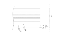
- FIG. 1B is a cross-sectional view showing the MQW constituting the light receiving layer 3.
- the light receiving layer 3 is a type 2 MQW in which InGaAs 3b and GaAsSb 3a are paired 3u.
- the number of pairs is 50 or more and 700 or less, and if the total thickness becomes excessive as will be described later, the sensitivity on the short wavelength side is lowered.
- the feature of the present invention is that, among the two compound semiconductors constituting the pair 3u, the layer having the higher valence band is made thinner than the layer having the lower valence band.
- the valence band is higher in GaAsSb3a than in InGaAs3b.
- the thickness of GaAsSb3a is made thinner than the thickness of InGaAs3b.
- InGaAs may be 5 nm / GaAsSb 2 nm.
- the light receiving element has the following purposes.
- the sensitivity should be as long as possible in the near infrared region.
- M2 High sensitivity in the entire near infrared wavelength region.
- M3 Avoid a sudden drop in sensitivity on the short wavelength side, and make the wavelength dependence moderate or preferably flat. In particular, avoid a sharp drop near the wavelength of 1.5 ⁇ m.
- FIG. 2 is a diagram for explaining the technical contents of the present invention.
- type 2 MQW light having a long wavelength, that is, a transition with a small energy difference is possible for electrons in the light receiving element.
- the electrons in the valence band of GaAsSb having the higher potential in the valence band transition to the conduction band of InGaAs, which has the lower valence band potential, so that a transition with a small energy difference or light with a long wavelength can be received.
- Holes generated in the valence band must move in the MQW 3 in order to reach the p-side electrode, and as described above, they disappear during this time and become a major factor in sensitivity reduction.
- the total thickness of MQW3 may be reduced.
- the reason is that the distance that must be moved against the well-type potential barrier is shortened. Further, an accompanying increase in electric field strength (an increase in driving force) can be expected.
- reducing the thickness of each layer uniformly to reduce the total thickness of the MQW has unacceptable side effects. For the explanation of the side effects, a little preparation is made below.
- the energy level of holes in the well-type potential in the valence band and the energy level of electrons in the well-type potential in the conduction band can be approximated by the following model. That is, the well width is finite and can be approximated by the energy level of electrons or holes in a well-type potential of infinite depth (height). According to the model, the energy level is expressed by the following equation (M).
- Ec n h 2 n c 2 / (8d 2 2 m 2 * ) (2)
- d 2 is the thickness of the lower valence band potential (eg, InGaAs).
- M 2 * effective mass of electrons
- the effective mass of holes (m 1 * ) in equation (1) is significantly different from the effective mass of electrons (m 2 * ) in equation (2), and the effective mass of holes is approximately larger than the effective mass of electrons. A point that is about 10 times larger is very important and forms the basis of the present invention.
- the description returns to the inconvenience when the MQW layers are uniformly thinned.
- the wavelength ⁇ max of the light having a limit wavelength that can be received is the difference between the ground level Ec 1 in the well-type potential of the conduction band of InGaAs and the ground level Eb 1 in the well-type potential of the valence band of GaAsSb.
- (Ec 1 ⁇ Eb 1 ) hc / ⁇ max is established.
- the energy difference (Ec 1 ⁇ Eb 1 ) becomes large, and the wavelength limit for receiving light is greatly shifted to the short wavelength side. That is, the critical wavelength that can be received unless the thickness is uniformly reduced increases the band gap or energy difference, and cannot be received. This is unacceptable for a light receiving element having the purpose of (M1) and trying to expand the light receiving sensitivity to the long wavelength side as much as possible.
- the effective mass of holes is about 10 times or more larger than the effective mass of electrons, so the hole ground level is originally about 10 times lower than that of electrons. (The difference from the vacuum state of each ground level). For this reason, when both GaAsSb and InGaAs are similarly reduced in thickness, the degree of increase in the ground level of electrons in the well-type potential of the conduction band in FIG. 2 is very large compared to holes. . In other words, it is about ten times larger than the degree of increase in the ground level of holes in the well-type potential of the valence band. When the thickness is uniformly reduced, the band gap or the energy difference is enlarged mainly by an increase in the ground level of electrons in the conduction band.
- the basic idea of the present invention is to reduce the total thickness of the MQW without significantly reducing the longest wavelength that can be received by reducing only the thickness d 1 of the higher valence band potential (GaAsSb). is there.
- the following advantages can be obtained.
- E1 Even if holes are generated far away from the p-side electrode, the total thickness Do is greatly reduced as shown in FIG. 3A, so that the holes can reach the p-side region or the p-side electrode.
- the possibility increases and the sensitivity can be improved. In particular, it light in the short wavelength side, so tends to generate immediately received by the positive holes contained in the MQW is strong, conventionally, as shown in FIG.
- both GaAsSb 103a and InGaAs 103b constituting the pair 103u have the same thickness of 5 nm as in the prior art.
- sensitivity can be ensured by reducing the total thickness of MQW according to the present invention. This not only improves the sensitivity over the wavelength range where light can be received, but also can more effectively suppress a drop in sensitivity particularly on the short wavelength side. As a result, the sensitivity with respect to the wavelength can be flattened or the fluctuation can be moderated.
- E2 When reverse bias voltage V of the same magnitude is applied, the electric field is increased by reducing the total thickness of MQW3.
- FIG. 4 shows a piping system of the all-organic MOVPE film forming apparatus 60 and the like.
- a quartz tube 65 is disposed in the reaction chamber (chamber) 63, and a raw material gas is introduced into the quartz tube 65.
- a substrate table 66 is disposed in the quartz tube 65 so as to be rotatable and airtight.
- the substrate table 66 is provided with a heater 66h for heating the substrate.
- the temperature of the surface of the wafer 50 a during film formation is monitored by the infrared temperature monitor device 61 through a window 69 provided in the ceiling of the reaction chamber 63.
- This monitored temperature is a temperature at the time of growth or a temperature called a film forming temperature or a substrate temperature.
- a temperature at the time of growth or a temperature called a film forming temperature or a substrate temperature.
- 400 ° C. or more and 560 ° C. or less are temperatures measured by this temperature monitor.
- the forced exhaust from the quartz tube 65 is performed by a vacuum pump.
- the source gas is supplied by a pipe communicating with the quartz tube 65.
- the all organic MOVPE method is characterized in that all raw material gases are supplied in the form of an organometallic gas.
- source gases such as impurities are not specified, but impurities are also introduced in the form of an organometallic gas.
- the raw material of the organometallic gas is put in a thermostat and kept at a constant temperature. Hydrogen (H 2 ) and nitrogen (N 2 ) are used as the carrier gas.
- the organometallic gas is transported by a transport gas, and is sucked by a vacuum pump and introduced into the quartz tube 65.
- the amount of the carrier gas is accurately adjusted by an MFC (Mass Flow Controller). Many flow controllers, solenoid valves, and the like are automatically controlled by a microcomputer.
- the film thickness of the MQW 3 is controlled by setting a program and controlling the flow rate controller, the electromagnetic valve, and the like.
- the n-type InP buffer layer 2 is epitaxially grown on the S-doped n-type InP substrate 1 to a film thickness of 150 nm.
- TeESi tetraethylsilane
- TMIn trimethylindium
- TBP tertiary butylphosphine
- the InP buffer layer 2 may be grown using an inorganic raw material PH 3 (phosphine). In the growth of the InP buffer layer 2, even if the growth temperature is about 600 ° C.
- the crystallinity of the InP substrate located in the lower layer is not deteriorated by heating at about 600 ° C.
- the MQW containing GaAsSb is formed in the lower layer, it is necessary to strictly maintain the substrate temperature within a range of, for example, a temperature of 400 ° C. or higher and 560 ° C. or lower. The reason is that when heated to about 600 ° C., the crystallinity of GaAsSb is greatly deteriorated due to heat damage, and when the InP cap layer is formed at a temperature lower than 400 ° C., the decomposition efficiency of the source gas is greatly increased. Therefore, the impurity concentration in the InP layer increases, and a high-quality InP cap layer cannot be obtained.
- a type 2 MQW light-receiving layer 3 having InGaAs / GaAsSb as a pair of quantum wells is formed.
- the thickness of GaAsSb3a in the quantum well is preferably about 2 nm, and the thickness of InGaAs3b is preferably 5 nm, for example.
- MQW light-receiving layer 3 is formed by stacking 250 pairs of quantum wells.
- triethylgallium (TEGa), tertiary butylarsine (TBAs), and trimethylantimony (TMSb) are used.
- TEGa, TMIn, and TBAs can be used.
- These source gases are all organometallic gases, and the molecular weight of the compound is large. Therefore, it can be completely decomposed at a relatively low temperature of 400 ° C. or higher and 560 ° C. or lower and contribute to crystal growth.
- the MQW light-receiving layer 3 can be made sharp in the composition change at the interface of the quantum well by the all-organic MOVPE method. As a result, highly accurate spectrophotometry can be performed.
- the raw material for Ga (gallium) may be TEGa (triethylgallium) or TMGa (trimethylgallium).
- the raw material for In (indium) may be TMIn (trimethylindium) or TEIn (triethylindium).
- TBAs tertiary butylarsine
- TMAs trimethylarsenic
- Sb antimony
- TMSb trimethylantimony
- TESb triethylantimony
- TIPSb triisopropylantimony
- TDMASb tridimethylaminoantimony
- a semiconductor element having a low MQW impurity concentration and excellent crystallinity can be obtained.
- a light receiving element when used in a light receiving element, a light receiving element with a small dark current and a high sensitivity can be obtained.
- an optical sensor device capable of capturing a clearer image such as an imaging device, can be obtained.
- the source gas is transported through the piping, introduced into the quartz tube 65, and exhausted. Any number of source gases can be supplied to the quartz tube 65 by increasing the number of pipes. For example, even a dozen kinds of source gases are controlled by opening and closing the electromagnetic valve.
- the flow rate of the source gas is controlled by a flow rate controller (MFC) shown in FIG. 4, and the flow into the quartz tube 65 is turned on and off by opening and closing the electromagnetic valve.
- MFC flow rate controller
- the quartz tube 65 is forcibly exhausted by a vacuum pump. There is no stagnation in the flow of the source gas, and it is performed smoothly and automatically. Therefore, the composition is switched quickly when forming the quantum well pair. As shown in FIG.
- the temperature distribution of the source gas does not have the directionality as the source gas inflow side or the outlet side. Further, since the wafer 50a revolves on the substrate table 66, the flow of the source gas near the surface of the wafer 50a is in a turbulent state, and even the source gas near the surface of the wafer 50a contacts the wafer 50a. Except for the raw material gas, it has a large velocity component in the flow direction from the introduction side to the exhaust side. Therefore, most of the heat flowing from the substrate table 66 to the source gas through the wafer 50a is always exhausted together with the exhaust gas. For this reason, a large temperature gradient or temperature step is generated in the vertical direction from the wafer 50a through the surface to the source gas space.
- the substrate temperature is heated to a low temperature range of 400 ° C. or more and 560 ° C. or less.
- a low temperature range 400 ° C. or more and 560 ° C. or less.
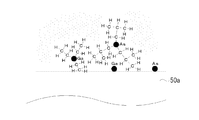
- FIG. 5A is a diagram showing the flow of organometallic molecules and the flow of temperature
- FIG. 5B is a schematic diagram of organometallic molecules on the substrate surface.
- organometallic molecules in a range in contact with the wafer surface and molecules located within the thickness range of several organometallic molecules from the wafer surface mainly contribute to crystal growth.
- the outer organometallic molecules are discharged out of the quartz tube 65 with almost no decomposition.
- the organometallic molecules located outside enter the replenishment.
- the range of the organometallic molecules that can participate in crystal growth is limited to a thin source gas layer on the surface of the wafer 50a by making the wafer surface temperature slightly higher than the temperature at which the organometallic molecules decompose. it can.
- phase separation occurs in the GaAsSb layer of the multiple quantum well structure when grown at a temperature of about 600 ° C., and the crystal growth surface of the multiple quantum well structure that is clean and excellent in flatness, and excellent A multiple quantum well structure having periodicity and crystallinity cannot be obtained.
- the growth temperature is set to a temperature range of 400 ° C. or more and 560 ° C. or less (deposition factor 2).
- This film formation method is an all-organic MOVPE method, and all the source gases are organometallic gases with high decomposition efficiency. (Film formation factor 3) strongly depends on film formation factor 1.
- an InGaAs diffusion concentration distribution adjustment layer 4 is located on the type 2 MQW light-receiving layer 3, and an InP cap layer 5 is formed on the InGaAs diffusion concentration distribution adjustment layer 4. positioned.
- the p-type region 6 is provided by selectively diffusing Zn of the p-type impurity from the opening of the selective diffusion mask pattern 36 provided on the surface of the InP cap layer 5.
- a pn junction 15 or a pi junction 15 is formed at the tip of the p-type region 6.
- a depletion layer is formed by applying a reverse bias voltage to the pn junction 15 or the pi junction 15 to capture charges due to photoelectron conversion, and to make the brightness of the pixel correspond to the amount of charges.
- the p-type region 6 or the pn junction 15 or the pi junction 15 is a main part constituting the pixel.
- the p-side electrode 11 that is in ohmic contact with the p-type region 6 is a pixel electrode, and reads the above charges for each pixel with the n-side electrode 12 that is set to the ground potential.
- the selective diffusion mask pattern 36 is left as it is on the surface of the InP cap layer around the p-type region 6. Further, a protective film such as SiON not shown is coated.
- the selective diffusion mask pattern 36 is left as it is.
- a surface level is formed at the boundary with the p-type region on the surface of the cap layer, and the dark current is formed. This is because of the increase.
- the growth continues in the same film forming chamber or quartz tube 65 by the all organic MOVPE method until the formation of the InP cap layer 5 is completed. That is, before the InP cap layer 5 is formed, the wafer 50a is not taken out from the film forming chamber, and the InP cap layer 5 is not formed by another film forming method.
- the MQW is formed as described above
- the interfaces 16 and 17 are not regrowth interfaces. For this reason, the concentrations of oxygen and carbon are both less than 1E17 (1 ⁇ 10 17 ) cm ⁇ 3 , and charge leakage does not occur particularly at the intersection line between the p-type region 6 and the interface 17.
- the InP cap layer 5 is formed, when the p-type impurity Zn is introduced from the InP cap layer 5 so as to reach the MQW light-receiving layer 3 by the selective diffusion method, the crystallinity is increased when high-concentration Zn enters the MQW.
- InGaAs diffusion concentration distribution layer 4 is provided for the adjustment.
- the InGaAs diffusion concentration distribution adjustment layer 4 may be arranged as described above, but may not be provided.
- the p-type region 6 is formed by the selective diffusion described above, and the pn junction 15 or the pi junction 15 is formed at the tip thereof. Even when the InGaAs diffusion concentration distribution adjusting layer 4 is inserted, since the InGaAs has a small band gap, the electric resistance of the light receiving element can be lowered even if it is non-doped. By reducing the electrical resistance, it is possible to improve the responsiveness and obtain a moving image with good image quality.
- the undoped InP cap layer 5 is epitaxially grown to a thickness of, for example, 0.8 ⁇ m by the all-organic MOVPE method continuously with the wafer 50a being placed in the same quartz tube 65. It is good.
- the growth temperature of the InP cap layer 5 can be made 400 ° C. or more and 560 ° C. or less, and further 535 ° C. or less.
- the MQW GaAsSb located under the InP cap layer 5 is not damaged by heat, and the MQW crystallinity is not impaired.
- the substrate temperature must be strictly maintained within a range of, for example, a temperature of 400 ° C. or higher and 560 ° C. or lower.
- the reason is that when heated to about 600 ° C., the crystallinity of GaAsSb is greatly deteriorated due to heat damage, and when the InP cap layer 5 is formed at a temperature lower than 400 ° C., the decomposition efficiency of the source gas is increased. Since it significantly decreases, the impurity concentration in the InP cap layer 5 increases, and the high quality InP cap layer 5 cannot be obtained.
- the interface between the InGaAs diffusion concentration distribution adjusting layer and the InP cap layer was a regrowth interface once exposed to the atmosphere.
- the regrowth interface by secondary ion mass spectrometry, one of oxygen concentration of 1E17 (1 ⁇ 10 17 ) cm ⁇ 3 or more and carbon concentration of 1E17 (1 ⁇ 10 17 ) cm ⁇ 3 or more is used. Can be specified by filling.
- the regrowth interface forms a crossing line with the p-type region, and a charge leak occurs at the crossing line, thereby significantly degrading the image quality.
- an InP cap layer is grown by a simple MOVPE method using phosphine (PH 3 ) as a raw material of phosphorus
- the decomposition temperature of phosphine is high, so that the occurrence of damage due to heat of GaAsSb located in the lower layer is induced and MQW is induced. It will harm the crystallinity.
- FIG. 6 is a flowchart of a manufacturing method of the light receiving element 50 of FIG. 1A.
- this manufacturing method only the organic metal gas is used as the source gas (deposition factor 3), the growth temperature is lowered (deposition factor 2), and until the formation of the InP cap layer 5 is completed. Therefore, it is important to have no recrystallization interface (deposition factor 4). As a result, it is possible to efficiently manufacture a large number of photodiodes having low charge leakage, excellent crystallinity, and having light receiving sensitivity in the near-infrared wavelength region.
- the light receiving element 50 has a single pixel. However, in the present invention, a plurality of pixels may be used and the arrangement may be one-dimensional or two-dimensional.
- FIG. 7 is a diagram showing the optical sensor device 10 including a light receiving element array (semiconductor element) 50 in which a plurality of pixels are arranged. Optical parts such as lenses are omitted. Although a protective film 43 made of a SiON film is shown in FIG. 7, it is actually arranged in FIG. 1A.
- the light receiving element array 50 has the same laminated structure as that of the light receiving elements shown in FIG. 1A, and is different in that a plurality of light receiving elements or pixels P are arranged.
- the interfaces 16 and 17 are not regrowth interfaces, and the concentration of impurities such as oxygen and carbon is as low as less than 1E17 (1 ⁇ 10 17 ) cm ⁇ 3 .
- the light receiving element array 50 is connected to a CMOS 70 constituting a readout circuit (Read-Out IC).
- the readout electrode (not shown) of the CMOS 70 and the pixel electrode (p-side electrode) 11 of the light receiving element array 50 are bonded with the bonding bump 39 interposed.
- a common ground electrode (n-side electrode) 12 for each pixel of the light receiving element array 50 and a ground electrode (not shown) of the CMOS 70 are joined via bumps 12b.
- An imaging device or the like can be obtained by combining the CMOS 70 and the light receiving element array 50 and integrating light reception information for each pixel.
- the light-receiving element array (semiconductor element) 50 of the present invention has sensitivity up to a long wavelength region and has a small dark current (leakage current), and therefore, inspection of living organisms such as animals and plants, environmental monitoring, etc. By using this, high-precision inspection can be performed.
- Example 1-Invariance of a long wavelength range in which light can be received by a light receiving element according to the present invention Using the light receiving element 50 having the same structure as that of the semiconductor element 50 shown in FIG. 1A as a basic structure, the following test body having a changed MQW structure was prepared, and verification of a long wavelength region capable of receiving light was performed. The manufacturing method followed the above-mentioned method. Evaluation of the long wavelength range which can receive light was performed by measuring PL (Photoluminescence) peak wavelength. The measurement temperature is room temperature (25 ° C.).
- the type 2 (InGaAs / GaAsSb) MQW of the present invention may or may not be a strain compensation superlattice structure.
- ⁇ is the lattice mismatch degree of the entire multi-quantum well structure
- ⁇ ⁇ ( ⁇ ) where the lattice mismatch degree of InGaAs in (GaAsSb / InGaAs) is ⁇ 1 and the lattice mismatch degree of GaAsSb is ⁇ 2.
- the strain can be changed by changing the composition of InGaAs and GaAsSb within a minute range and changing the degree of lattice mismatch.
- Each test body shown below (examples of the present invention and comparative examples) was obtained by changing the composition to change the strain ( ⁇ ), and each test body belongs to the number of strain values, Those having the same MQW thickness configuration were displayed as the same specimen.
- ⁇ Invention Sample A> (InGaAs thickness 5 nm / GaAsSb 2 nm) as one pair, 250 pairs of MQW were obtained.
- the total thickness of MQW is 1750 nm (1.75 ⁇ m).
- ⁇ Comparative Example B1> InGaAs thickness 5 nm / GaAsSb 5 nm) was used as one pair, and 250 pairs of MQW were obtained.
- the total thickness of MQW is 2500 nm (2.5 ⁇ m).
- the total thickness of MQW is 1750 nm (1.75 ⁇ m).
- the measurement result of the PL peak wavelength (median value) is shown in FIG. FIG. 8 clarifies the following.
- R1 Even when the MQW thickness configuration is the same, the present invention example A may exhibit the same PL peak wavelength as that of the comparative example B2 in consideration of the effect that the PL peak wavelength becomes shorter when the strain ( ⁇ ) is positively increased.
- the thickness of InGaAs in the MQW of Invention Example A is 5 nm, which is the same as the thickness of InGaAs in Comparative Example B1.
- Comparative Example B2 in which the thickness of InGaAs is as thin as 3.5 nm, the PL peak wavelength is greatly shifted in the direction of shortening the wavelength.
- Example A of the present invention the PL peak wavelength is the same as that in Comparative Example B1 as described above, despite the fact that the thickness of GaAsSb is as extremely thin as 2 nm. This result shows that the PL peak wavelength hardly changes if the thickness of InGaAs having the lower potential of one valence band forming the MQW pair is the same in the present invention. This proves that the above estimation based on the equations (1-1) and (2-1) is applied with a good approximation. (R2) In addition, in Invention Example A, the total thickness of MQW was reduced from 2.5 ⁇ m of Comparative Example B1 to 1.75 ⁇ m to 70% of the original total thickness.
- the rate at which holes disappear during movement through MQW can be greatly reduced, and the electric field for accelerating holes and electrons can be improved by about 1.43 times while applying the same bias voltage.
- the sensitivity of the light receiving element is improved over the entire wavelength range.
- light on the short wavelength side is easily received at the entrance (end position) of the MQW, and thus is easily affected by the total thickness.
- the sensitivity on the short wavelength side which is lower than that on the long wavelength side, can be improved to the same level as that on the long wavelength side by reducing the total thickness.
- FIG. 9 is a diagram showing the wavelength dependence of sensitivity in Comparative Example B1 (total thickness 2.5 ⁇ m) and Comparative Example B2 (total thickness 1.75 ⁇ m). The wavelength range is limited to a wavelength of 2 ⁇ m or less where both can be compared. According to FIG.
- Comparative Example B2 where the MQW total thickness is 1.75 ⁇ m, the sensitivity is almost flat in the wavelength range of 1.3 ⁇ m-2.0 ⁇ m. From Examples 1 and 2 above, the following was verified. By reducing the thickness of one layer (for example, GaAsSb layer) having a higher valence band that constitutes the MQW and maintaining the thickness of the other layer (for example, InGaAs layer) to be the same as the conventional one, it is possible to receive light. The limit on the wavelength side is almost unchanged. On top of that, the total thickness of MQW decreases as the thickness of the GaAsSb layer is reduced. Therefore, the sensitivity is improved over the entire wavelength range, and the sensitivity on the short wavelength side, which is lowered compared to the long wavelength side, is particularly the same as that on the long wavelength side. The sensitivity level can be improved.
- one layer for example, GaAsSb layer
- InGaAs layer InGaAs layer
- the light receiving element of the present invention it is possible to prevent a drop in sensitivity particularly on the short wavelength side while improving the sensitivity over the entire wavelength range without greatly affecting the wavelength limit of light that can be received using Type 2 MQW. be able to.
- the wavelength dependence of sensitivity is relatively flat. For example, substances with multiple absorption spectra (for example, water) over a wide wavelength range in the near infrared region, and materials and phenomena with broad absorption bands can be analyzed with high accuracy. It becomes possible to do.
Abstract
Description
上記の受光素子は、受光層を基準にしてInP基板と逆側のキャップ層をp導電型とし、InP基板をn導電型として、光入射はInP基板の裏面側から行う構造をとる。
また、非特許文献2には、上記と同様の構造のフォトダイオードについて、感度の波長依存性が開示されている。感度は、波長に対して平坦ではなく、強い波長依存性を示す。 Non-Patent
The light receiving element has a structure in which the cap layer on the opposite side to the InP substrate is a p-conductivity type with respect to the light-receiving layer, the InP substrate is an n-conductivity type, and light is incident from the back side of the InP substrate.
Non-Patent
本発明は、タイプ2のMQWを持つ受光素子において、受光可能な全波長域にわたって感度を向上させながら、短波長域での感度の落ち込みを防止することができる、受光素子、その受光素子を用いた光学センサ装置、および受光素子の製造方法を提供することを目的とする。なお、受光素子は、画素が単一の素子でもよいし、一次元または二次元にアレイ化された素子でもよい。 The sensitivity of the photodiode having the MQW of
The present invention relates to a light receiving element having an MQW of
電子は伝導帯を移動してn側電極に、また正孔は価電子帯を移動してp側電極に、到達することで、上記電荷または電流が検知される。各キャリア(電子、正孔)の移動速度を見積もるとき、これから説明するように有効質量の大きさが大きく影響する。化合物半導体における電子の伝導帯における有効質量は、0.05m(m:自由電子の質量)程度であるのに対して、価電子帯における正孔の有効質量(重い(heavy)ほうの正孔)は大きく、たとえば電子の10倍程度以上である。 Generally, when light reception (light absorption) occurs in the light receiving layer, electrons in the valence band are excited to the conduction band, and vacancies are generated in the valence band. That is, an electron / hole pair is formed by light reception. In order to detect that the above light reception has occurred in a predetermined pixel, the electrons reach the n-side electrode and the vacancies reach the p-side electrode and need to be detected as charges or currents. One of the n-side electrode and the p-side electrode needs to be arranged for each pixel.
Electrons move through the conduction band and reach the n-side electrode, and holes move through the valence band and reach the p-side electrode, whereby the charge or current is detected. When estimating the moving speed of each carrier (electron, hole), the size of the effective mass greatly affects as described below. The effective mass in the conduction band of electrons in a compound semiconductor is about 0.05 m (m: mass of free electrons), whereas the effective mass of holes in the valence band (heavy holes) Is large, for example, about 10 times or more of electrons.
タイプ2のMQWでは、長波長側の光の受光は、高いほうの層と低いほうの層との界面で生じる。高いほうの層の価電子帯の電子は、低いほうの層の伝導帯へ、小さいエネルギの光(より長い波長の光)の吸収で励起される。より長波長側への受光感度の拡大のために、タイプ2のMQWが用いられる理由はここにある。このためタイプ2のMQWでは、所定数以上のペア数(界面数)がないと、長波長域の感度を実用レベル以上にすることができない。しかし、あまりペア数を多くするとMQWの総厚みが過大になり、正孔のp側電極への到達を阻害して、逆に感度を低下させる。正孔がMQW中を移動中に消滅してp側電極に到達できないからである。本発明では、ペア数を50以上とする。上限はとくに設けないが、正孔の消滅の大きな要因にならない程度、たとえば700以下とするのがよい。 The phenomenon peculiar to the reception of the
In
(F1)入射面とp側電極とがMQWを挟むような位置関係の場合、短波長側の光は入射面に近い位置のMQW端で受光される傾向が強い。このため、生じた正孔・電子のうち正孔はMQWのほとんど全厚みを移動しなければp側電極に到達できない。正孔はMQWを移動途中で消滅する割合が多くなり、この結果、感度は低下する。短波長の光ほどMQW内のp側電極から遠い位置で受光され、正孔が生じる傾向があるので、正孔の移動中の消滅による感度の低下は、短波長において生じやすい。
(F2)入射面とn側電極とがMQWを挟むような位置関係の場合、p側電極は入射面との間にMQWを挟むことなく、入射面近くに位置する。受光で生じた伝導帯の電子は、MQWのほとんど全厚みを移動しなければn側電極に到達できない。電子は、ほとんど全MQWの層を移動しなければならないものの、有効質量が正孔に比べて10倍程度小さいため、移動しやすく感度低下への影響はそれほど大きくはない。しかし、受光がMQWの端ではなくMQWの厚み中心付近で生じた場合、そこで生じた正孔は、多くのMQWの層を移動しなければ、p側電極に到達しないので、やはり感度低下の原因になる。
(F2)の場合は、(F1)の場合に比べて、短波長域の感度低下への影響は大きくないかもしれないが、それでも、正孔のMQW移動中の消滅による感度低下は、明確にあり、無視することはできない。 In the light receiving element, the following two arrangement configurations (F1) and (F2) cover all arrangement configurations, but are classified for the purpose of organizing the concept. For both arrangements, the present invention has a beneficial effect.
(F1) When the incident surface and the p-side electrode are in a positional relationship such that the MQW is sandwiched between them, the light on the short wavelength side tends to be received at the MQW end near the incident surface. For this reason, of the generated holes / electrons, the holes cannot reach the p-side electrode unless they move through almost the entire thickness of the MQW. Holes are more likely to disappear during the movement of MQW, resulting in a decrease in sensitivity. Since shorter wavelength light is received at a position farther from the p-side electrode in the MQW and tends to generate holes, a decrease in sensitivity due to annihilation during the movement of holes tends to occur at shorter wavelengths.
(F2) When the incident surface and the n-side electrode are in a positional relationship such that the MQW is sandwiched, the p-side electrode is positioned near the incident surface without sandwiching the MQW between the incident surface and the n-side electrode. Electrons in the conduction band generated by light reception cannot reach the n-side electrode unless they move through almost the entire thickness of the MQW. Although electrons almost have to move through the entire MQW layer, since the effective mass is about 10 times smaller than holes, the electrons move easily, and the influence on the sensitivity reduction is not so great. However, when light reception occurs not near the end of the MQW but near the center of the thickness of the MQW, the holes generated there do not reach the p-side electrode unless moving through many MQW layers. become.
In the case of (F2), compared to the case of (F1), the influence on the sensitivity decrease in the short wavelength region may not be great, but the sensitivity decrease due to the disappearance of holes during the MQW movement is still clearly Yes, it cannot be ignored.
(e1)タイプ2のMQWにおいて受光可能な波長限界は、高いほうの層の価電子帯の基底状態のエネルギと、低いほうの層の伝導帯の基底状態のエネルギとの差によって決まる。一般的に、量子井戸層の厚みを薄くすると、電子に対する基底状態のエネルギは大きく上昇するが、正孔に対する基底状態のエネルギの上昇は小さい。その理由は、電子または正孔のエネルギ準位に対して、有効質量が大きく影響し、有効質量が大きいとエネルギ準位は低く、基底状態のエネルギレベルも低いからである。高いほうの層(その価電子帯に正孔が生成する)の厚みを薄くして、低いほうの層(その伝導帯に電子が生成する)の厚みを所定レベル以上とすることで、受光可能な波長限界はほとんど変化しない。
その波長限界を含む波長域の感度については、50ペア以上のMQWとすることで、高い感度を保持することができる。
(e2)受光待機状態では、両電極間に逆バイアス電圧を印加して、MQW内に電界をかける。正孔および電子は、この電界によって駆動されてMQW中を移動する。本発明のように、MQWの総厚みを薄くすることで、一定のバイアス電圧によってMQW内に生じる電界の強度を高めることができる。この電界強度の向上によって正孔の消滅を抑制して感度を高めることができる。
(e3)上記正孔の消滅の抑制作用は、受光された光の波長によらず有効である。所定ペア数以上を確保しながらMQWの総厚みを薄くすることによって、上記(F1)のような正孔のMQW内での消滅を軽減することができ、その結果、特に短波長側での感度の低下を防止する上で、有効である。この結果、感度は波長に対して平坦、もしくは緩やかな変動を示すようになる。 In the case of both arrangement configurations (F1) and (F2), the following effects (e1) to (e3) can be obtained by reducing the thickness of the higher layer while maintaining 50 pairs or more. In the following description, the wavelength limit refers to a longer wavelength limit.
(E1) The wavelength limit at which light can be received in
As for the sensitivity in the wavelength region including the wavelength limit, high sensitivity can be maintained by setting MQW of 50 pairs or more.
(E2) In a light reception standby state, a reverse bias voltage is applied between both electrodes to apply an electric field in the MQW. Holes and electrons move through the MQW driven by this electric field. By reducing the total thickness of the MQW as in the present invention, the strength of the electric field generated in the MQW by a constant bias voltage can be increased. By improving the electric field strength, the disappearance of holes can be suppressed and the sensitivity can be increased.
(E3) The effect of suppressing the disappearance of holes is effective regardless of the wavelength of the received light. By reducing the total thickness of the MQW while ensuring a predetermined number of pairs or more, the annihilation of holes in the MQW as described in (F1) can be reduced, and as a result, the sensitivity particularly on the short wavelength side. This is effective in preventing a decrease in the amount of light. As a result, the sensitivity is flat with respect to the wavelength or shows a gentle fluctuation.
InP基板を用いる場合、技術実績が多く累積されているp型不純物のZnの取り扱いの容易性、および、画素の電極に対する読み出し回路(ROIC:Read Out IC)の配置のし易さ、の2つの理由から基板の裏面入射とするのが普通である。このため、上記の配置とする場合が多い。すなわち上記(F1)の配置構成の場合が多い。n側電極は、グランド電極となる。 A cap layer located on the light receiving layer is provided, and the pixel region in the cap layer is of p conductivity type, and the back surface of the substrate can be a light incident surface. In this case, the p-side electrode is located on a p-conductivity type pixel. Holes generated by light reception tend to disappear while moving in the valence band toward the p-side electrode. As a result, sensitivity decreases. In particular, when light is received at the end of the MQW close to the substrate, the holes generated there do not contribute to sensitivity unless they move through almost the entire thickness of the MQW. As described above, in the present invention, the total thickness of MQW can be reduced without significantly affecting the wavelength limit of light reception. As a result, it is possible to improve the sensitivity of light on the short wavelength side that is easily received at the end of the MQW.
When using an InP substrate, there are two approaches: easy handling of Zn, which is a p-type impurity, which has accumulated many technical achievements, and easy placement of a readout circuit (ROIC: Read Out IC) with respect to a pixel electrode. For the reason, it is normal to use the back surface of the substrate. For this reason, the above arrangement is often used. That is, there are many cases of the arrangement configuration (F1). The n-side electrode becomes a ground electrode.
これによって、受光可能な波長限界が2.5μm以上で3μmに近い範囲までをカバー可能な、高品位の受光素子を得ることができる。 MQW is a
As a result, it is possible to obtain a high-quality light-receiving element that can cover the wavelength limit of light reception that is 2.5 μm or more and close to 3 μm.
これによって、短波長側の感度が過小なためにスペクトル解析などの情報処理等に支障をきたすことがなくなる。 The light receiving element can have a sensitivity to light having a wavelength of 1500 nm of 0.5 A / W or more.
As a result, since the sensitivity on the short wavelength side is too small, information processing such as spectrum analysis is not hindered.
再成長界面には、酸素や炭素等の不純物が濃縮するため、再成長界面上に形成されたエピタキシャル層の結晶性を劣化させ、暗電流の増大等をもたらす。上記の部分に再成長界面を持たないことで、良好な結晶層を得ることができ、暗電流を低減させることができる。 It is preferable not to have a regrowth interface between the top surface of the MQW and the bottom surface of the cap layer.
Since impurities such as oxygen and carbon are concentrated on the regrowth interface, the crystallinity of the epitaxial layer formed on the regrowth interface is deteriorated, resulting in an increase in dark current and the like. By not having a regrowth interface in the above portion, a good crystal layer can be obtained and dark current can be reduced.
これによって、近赤外域に感度を持ち、暗電流が低い高品位の受光素子を用いて、生体、環境など、これまで、冷却装置なしではセンシングが不可能であった分野において、常温使用が可能な小型の装置を提供することができる。仮に、冷却装置を要する場合、そのための電源、または液体窒素等の供給が必要となる。このため、サイズ、冷却維持、冷却維持のためのコスト、などの点で大きな制約を課すことになる。本発明では、このような理由で不可能であった分野に対して高精度のセンシングを可能にする。 The optical sensor device of the present invention is characterized by using any of the light receiving elements described above.
As a result, high-quality light-receiving elements that have sensitivity in the near-infrared region and low dark current can be used at room temperature in fields that have previously been impossible to sense without cooling devices, such as living organisms and the environment. And a small device can be provided. If a cooling device is required, power for that purpose or supply of liquid nitrogen or the like is required. For this reason, large restrictions are imposed in terms of size, cooling maintenance, and cost for cooling maintenance. The present invention enables highly accurate sensing for a field that has been impossible for such a reason.
上記の方法によって、受光可能な波長限界を大きく変えずに、感度の高い受光素子を簡単に得ることができる。 The method for manufacturing a light receiving element of the present invention manufactures a light receiving element formed on a substrate of a III-V compound semiconductor and having pixels. The manufacturing method includes a step of growing a
By the above method, a highly sensitive light receiving element can be easily obtained without greatly changing the wavelength limit of light reception.
これによって、結晶性に優れた積層体をMQW上に形成することができる。 After the step of forming MQW, the method further includes a step of forming a layer including a group III-V compound semiconductor. Between the step of forming MQW and the step of forming a layer including a group III-V compound semiconductor, From the start of the growth of MQW to the end of the growth of the layer containing the III-V compound semiconductor, the same growth tank is formed by the all-organic vapor phase growth method (the all-organic MOVPE method) so as not to include the step of forming the growth interface. Can grow within.
Thereby, a laminate having excellent crystallinity can be formed on the MQW.
(n型InP基板1/n型InPバッファ層(厚み150nm)2/タイプ2(InGaAs/GaAsSb)MQWの受光層3/InGaAs拡散濃度分布調整層4/InPキャップ層5)
p型領域6はInPキャップ層5の表面からMQWの受光層3にまで届くように位置する。このp型領域6はSiN膜の選択拡散マスクパターン36の開口部から、p型不純物のZnが選択拡散されることで形成される。上記SiN膜の選択拡散マスクパターン36を用いて拡散することによって、受光素子50の周縁部の内側に、平面的に見て周囲限定されてZnが拡散導入される。p型領域6にはAuZnによるp側電極11が、またInP基板1の裏面にはAuGeNiのn側電極12が、それぞれオーミック接触するように設けられている。この場合、InP基板1にはn型不純物がドープされており、所定レベルの導電性を有する。ただし、InP基板1は、導電性を持たなくてもよく、この場合、n側電極12は、n型InPバッファ層2にオーミック接触するように配置することになる。InP基板1の裏面には、またSiONの反射防止膜35を設けてあり、InP基板の裏面側から光を入射する。図1Aに示す受光素子50は、したがって、(F1)の配置構成の場合に該当する。
タイプ2のMQWの受光層3には、上記のp型領域6の境界フロントに対応する位置にpn接合15が形成され、上記のp側電極11およびn側電極12間に逆バイアス電圧を印加することにより、n型不純物濃度が低い側(n型不純物バックグラウンド)により広く空乏層を生じる。MQWの受光層3におけるn型不純物バックグラウンドは、n型不純物濃度(キャリア濃度)で5E15(5×10¹⁵)cm-3程度またはそれ以下である。そして、pn接合の位置15は、多重量子井戸の受光層3のバックグラウンド(n型キャリア濃度)と、p型不純物のZnの濃度プロファイルとの交点で決まる。InGaAs拡散濃度分布調整層4は、受光層3を構成するMQW内でのp型不純物の濃度分布を調整するために配置される。InGaAs拡散濃度分布調整層4はなくてもよい。受光層3内では、Zn濃度は5E16(5×10¹⁶)cm-3以下にするのがよい。 FIG. 1A is a diagram showing a
(N-
The p-
In the
本発明の特徴は、ペア3uを構成する2つの化合物半導体のうち、価電子帯が高いほうの層の厚みを、低いほうの層の厚みよりも薄くする点に特徴がある。上記のInGaAsとGaAsSbとの場合では、価電子帯は、GaAsSb3aのほうがInGaAs3bよりも高い。このため、GaAsSb3aの厚みを、InGaAs3bの厚みよりも薄くする。具体的な厚みをあげれば、たとえばInGaAs5nm/GaAsSb2nm、とするのがよい。
本発明では、受光素子は、つぎの目的を有する。
(M1)近赤外域のできるだけ長波長側に感度を持つようにする。
(M2)近赤外の全体の波長域で高い感度を持つ。
(M3)短波長側での感度の急激な落ち込みを避けて、波長依存性を緩やかか、望ましくは平坦にする。とくに波長1.5μm付近での急激な落ち込みを避ける。 FIG. 1B is a cross-sectional view showing the MQW constituting the
The feature of the present invention is that, among the two compound semiconductors constituting the
In the present invention, the light receiving element has the following purposes.
(M1) The sensitivity should be as long as possible in the near infrared region.
(M2) High sensitivity in the entire near infrared wavelength region.
(M3) Avoid a sudden drop in sensitivity on the short wavelength side, and make the wavelength dependence moderate or preferably flat. In particular, avoid a sharp drop near the wavelength of 1.5 μm.
En=h2n2/(8d2m*)・・・・・・・・・・・(M)
n:励起状態の指数または励起レベル(基底状態ではn=1)、h:プランク定数、d:井戸型ポテンシャルの幅(サイズ)、m*:電子または正孔の有効質量
上記の模型をGaAsSbの価電子帯の井戸型ポテンシャル内の正孔に適用すると、つぎの(1)式が得られる。
価電子帯の井戸型ポテンシャル内の正孔のエネルギ準位:
Ebn=h2nb 2/(8d1 2m1 *)・・・・・・・・(1)
ここで、nb:価電子帯の井戸型ポテンシャル内での正孔の励起状態を示す指数(基底状態ではnb=1)、d1:価電子帯のポテンシャルが高いほう(例:GaAsSb)の厚み、m1 *:正孔の有効質量
とくに基底準位は、Eb1=h2/(8d1 2m1 *)・・・(1-1)である。
一方、上記の模型をInGaAsの伝導帯の井戸型ポテンシャル内の電子に適用すると、(2)式が得られる。
伝導帯の井戸型ポテンシャル内の電子のエネルギ準位:
Ecn=h2nc 2/(8d2 2m2 *)・・・・・・・・(2)
ここで、nc:伝導帯の井戸型ポテンシャル内での電子の励起状態を示す指数(基底状態ではnc=1)、d2:価電子帯のポテンシャルが低いほう(例:InGaAs)の厚み、m2 *:電子の有効質量
とくに基底準位は、Ec1=h2/(8d2 2m2 *)・・・(2-1)である。
(1)式における正孔の有効質量(m1 *)と、(2)式おける電子の有効質量(m2 *)とは大きく異なり、正孔の有効質量が、電子の有効質量よりもおよそ10倍程度以上大きい点が非常に重要であり、本発明の根底をなす。 The energy level of holes in the well-type potential in the valence band and the energy level of electrons in the well-type potential in the conduction band can be approximated by the following model. That is, the well width is finite and can be approximated by the energy level of electrons or holes in a well-type potential of infinite depth (height). According to the model, the energy level is expressed by the following equation (M).
En = h 2 n 2 / (8d 2 m * ) (M)
n: exponent or excitation level of excited state (n = 1 in the ground state), h: Planck's constant, d: width of well-type potential (size), m * : effective mass of electron or hole When applied to holes in a well-type potential in the valence band, the following equation (1) is obtained.
Energy levels of holes in a well-type potential in the valence band:
Eb n = h 2 n b 2 / (
Where n b is an index indicating the excited state of holes in the well-type potential of the valence band (n b = 1 in the ground state), d 1 is the higher potential of the valence band (eg, GaAsSb) , M 1 * : effective mass of holes In particular, the ground level is Eb 1 = h 2 / (8d 1 2 m 1 * ) (1-1).
On the other hand, when the above model is applied to electrons in the well-type potential of the InGaAs conduction band, equation (2) is obtained.
Energy levels of electrons in the well-type potential of the conduction band:
Ec n = h 2 n c 2 / (8d 2 2 m 2 * ) (2)
Here, n c is an index indicating the excited state of electrons in the well-type potential of the conduction band (n c = 1 in the ground state), d 2 is the thickness of the lower valence band potential (eg, InGaAs). , M 2 * : effective mass of electrons In particular, the ground level is Ec 1 = h 2 / (8d 2 2 m 2 * ) (2-1).
The effective mass of holes (m 1 * ) in equation (1) is significantly different from the effective mass of electrons (m 2 * ) in equation (2), and the effective mass of holes is approximately larger than the effective mass of electrons. A point that is about 10 times larger is very important and forms the basis of the present invention.
MQWの総厚みを薄くするために、各層の厚みを一様に減少させると仮定する。すると上記(1-1)式および(2-1)式に従って、価電子帯の井戸型ポテンシャル内の正孔の基底準位、および伝導帯の井戸側ポテンシャル内の電子の基低準位は、お互いに遠ざかるように(エネルギ差を増す方向に)、変化する。すなわち、正孔の基底準位は、Eb1=h2/(8d1 2m1 *)における厚みd1を小さくする程に応じて大きくなる。また、電子の基底準位は、Ec1=h2/(8d2 2m2 *)における厚みd2を小さくする程に応じて大きくなる。この結果、エネルギ差(Ec1-Eb1)は大きくなり、受光可能な波長限界は短波長側に大きくシフトする。すなわち、一様に厚みを薄くしなければ受光できた限界波長は、バンドギャップまたはエネルギ差が大きくなって、受光できなくなる。これは、上記(M1)の目的を持ち、受光感度をできるだけ長波長側に拡大しようとする受光素子にとって受け入れることはできない。 After the above preparation, the description returns to the inconvenience when the MQW layers are uniformly thinned. In receiving light of a limit wavelength that can be received, electrons located in the ground state (level) in the valence band of GaAsSb transition to the ground state in the conduction band of InGaAs. That is, the wavelength λmax of the light having a limit wavelength that can be received is the difference between the ground level Ec 1 in the well-type potential of the conduction band of InGaAs and the ground level Eb 1 in the well-type potential of the valence band of GaAsSb. Corresponding to That is, (Ec 1 −Eb 1 ) = hc / λmax is established. It should be noted that there are various forbidden laws for transition of electrons, and it may not be a simple transition as shown in FIG. 2, but it is assumed that such a forbidden law is not applied. Even under such assumptions, the transition scheme shown in FIG. 2 is still valid as a basis for a semi-quantitative idea.
Assume that the thickness of each layer is uniformly reduced to reduce the total MQW thickness. Then, according to the above formulas (1-1) and (2-1), the ground level of holes in the well-type potential of the valence band and the group low level of electrons in the well-side potential of the conduction band are It changes to move away from each other (in the direction of increasing energy difference). That is, the ground ground level increases as the thickness d 1 in Eb 1 = h 2 / (8d 1 2 m 1 * ) is decreased. Further, the electron ground level increases as the thickness d 2 in Ec 1 = h 2 / (8d 2 2 m 2 * ) is decreased. As a result, the energy difference (Ec 1 −Eb 1 ) becomes large, and the wavelength limit for receiving light is greatly shifted to the short wavelength side. That is, the critical wavelength that can be received unless the thickness is uniformly reduced increases the band gap or energy difference, and cannot be received. This is unacceptable for a light receiving element having the purpose of (M1) and trying to expand the light receiving sensitivity to the long wavelength side as much as possible.
本発明の基本思想は、価電子帯のポテンシャルが高いほう(GaAsSb)の厚みd1のみを減少させることによって、受光可能な最長波長を大きく低下させることなく、MQWの総厚みを減少させることにある。これによって、次の利点を得ることができる。
(E1)正孔は、たとえp側電極から遠く離れた箇所で生成しても、図3Aに示すように、総厚みDoは大きく減少しているので、p側領域またはp側電極に到達できる可能性は高くなり、感度を向上させることができる。とくに、短波長側の光は、MQWに入って直ぐに受光されて正孔を発生させる傾向が強いので、従来は、図3Bに示すように、大きい総厚みDLのMQW3では途中で消滅することが多かった。図3Bでは、ペア103uを構成するGaAsSb103aおよびInGaAs103bは、両方とも、従来の同じ程度の厚み5nmを有する。しかし、本発明によってMQWの総厚みを減少させることで、感度を確保することができる。
これによって、受光可能な波長域にわたって感度を向上させるだけでなく、とくに短波長側での感度の落ち込みをより効果的に抑制することができる。この結果、波長に対して感度を平坦、もしくは変動を緩やかにすることができる。
(E2)同じ大きさの逆バイアス電圧Vを印加した場合、MQW3の総厚みを薄くすることで、電界は大きくなる。すなわち、Do<DLのとき、(V/Do)>(V/DL)である。この結果、逆バイアス電圧による電界は、正孔および電子をより強く駆動(加速)してそれぞれの電極に向かわせることができる。
(E3)繰り返しになるが、上記のように、価電子帯のポテンシャルが高いほうの層(たとえばGaAsSb)の厚みを薄くして、ペアを組む他方の層の厚みを減少させないことで、受光可能な最長波長をほとんど変えないようにできる。 However, paying attention to the effective mass, the effective mass of holes is about 10 times or more larger than the effective mass of electrons, so the hole ground level is originally about 10 times lower than that of electrons. (The difference from the vacuum state of each ground level). For this reason, when both GaAsSb and InGaAs are similarly reduced in thickness, the degree of increase in the ground level of electrons in the well-type potential of the conduction band in FIG. 2 is very large compared to holes. . In other words, it is about ten times larger than the degree of increase in the ground level of holes in the well-type potential of the valence band. When the thickness is uniformly reduced, the band gap or the energy difference is enlarged mainly by an increase in the ground level of electrons in the conduction band.
The basic idea of the present invention is to reduce the total thickness of the MQW without significantly reducing the longest wavelength that can be received by reducing only the thickness d 1 of the higher valence band potential (GaAsSb). is there. As a result, the following advantages can be obtained.
(E1) Even if holes are generated far away from the p-side electrode, the total thickness Do is greatly reduced as shown in FIG. 3A, so that the holes can reach the p-side region or the p-side electrode. The possibility increases and the sensitivity can be improved. In particular, it light in the short wavelength side, so tends to generate immediately received by the positive holes contained in the MQW is strong, conventionally, as shown in FIG. 3B, which disappears in the middle in MQW3 large total thickness D L There were many. In FIG. 3B, both
This not only improves the sensitivity over the wavelength range where light can be received, but also can more effectively suppress a drop in sensitivity particularly on the short wavelength side. As a result, the sensitivity with respect to the wavelength can be flattened or the fluctuation can be moderated.
(E2) When reverse bias voltage V of the same magnitude is applied, the electric field is increased by reducing the total thickness of MQW3. That is, <time D L, (V / Do) > Do is (V / D L). As a result, the electric field due to the reverse bias voltage can drive (accelerate) holes and electrons more strongly and direct them toward the respective electrodes.
(E3) Repeatedly, as described above, it is possible to receive light by reducing the thickness of the layer having the higher valence band potential (for example, GaAsSb) and reducing the thickness of the other layer forming the pair. The longest wavelength can be hardly changed.
次に製造方法について説明する。InP基板1を準備して、その上に、InPバッファ層2/タイプ2(InGaAs/GaAsSb)MQWの受光層3/InGaAs拡散濃度分布調整層4/InPキャップ層5、を全有機MOVPE法で成長する。
図4に全有機MOVPE法の成膜装置60の配管系統等を示す。反応室(チャンバ)63内に石英管65が配置され、その石英管65に、原料ガスが導入される。石英管65中には、基板テーブル66が、回転自在に、かつ気密性を保つように配置される。基板テーブル66には、基板加熱用のヒータ66hが設けられる。成膜途中のウエハ50aの表面の温度は、反応室63の天井部に設けられたウィンドウ69を通して、赤外線温度モニタ装置61によりモニタされる。このモニタされる温度が、成長するときの温度、または成膜温度もしくは基板温度等と呼ばれる温度である。本発明における製造方法における、温度400℃以上かつ560℃以下でMQWを形成する、というときの400℃以上および560℃以下は、この温度モニタで計測される温度である。石英管65からの強制排気は真空ポンプによって行われる。 <How to grow MQW>
Next, a manufacturing method will be described. An
FIG. 4 shows a piping system of the all-organic MOVPE
MQW3の膜厚の制御は、プログラムを設定して、上記の流量制御器、電磁弁等を制御することで行われる。 The source gas is supplied by a pipe communicating with the
The film thickness of the
原料ガスは、図4に示す流量制御器(MFC)によって流量を制御された上で、石英管65への流入を電磁バルブの開閉によってオンオフされる。そして、石英管65からは、真空ポンプによって強制的に排気される。原料ガスの流れに停滞が生じる部分はなく、円滑に自動的に行われる。よって、量子井戸のペアを形成するときの組成の切り替えは、迅速に行われる。
図4に示すように、基板テーブル66は回転するので、原料ガスの温度分布は、原料ガスの流入側または出口側のような方向性をもたない。また、ウエハ50aは、基板テーブル66上を公転するので、ウエハ50aの表面近傍の原料ガスの流れは、乱流状態にあり、ウエハ50aの表面近傍の原料ガスであっても、ウエハ50aに接する原料ガスを除いて導入側から排気側への大きな流れ方向の速度成分を有する。したがって、基板テーブル66からウエハ50aを経て、原料ガスへと流れる熱は、大部分、常時、排気ガスと共に排熱される。このため、ウエハ50aから表面を経て原料ガス空間へと、垂直方向に大きな温度勾配または温度段差が発生する。
さらに、本発明の実施の形態では、基板温度を400℃以上かつ560℃以下という低温域に加熱される。このような低温域の基板表面温度でTBAsなどを原料とした全有機MOVPE法を用いる場合、その原料の分解効率が良いので、ウエハ50aにごく近い範囲を流れる原料ガスで多重量子井戸構造の成長に寄与する原料ガスは、成長に必要な形に効率よく分解したものに限られる。 Next, the flow state of the source gas when the multiple
The flow rate of the source gas is controlled by a flow rate controller (MFC) shown in FIG. 4, and the flow into the
As shown in FIG. 4, since the substrate table 66 rotates, the temperature distribution of the source gas does not have the directionality as the source gas inflow side or the outlet side. Further, since the
Furthermore, in the embodiment of the present invention, the substrate temperature is heated to a low temperature range of 400 ° C. or more and 560 ° C. or less. In the case of using the all organic MOVPE method using TBAs or the like as a raw material at the substrate surface temperature in such a low temperature region, since the decomposition efficiency of the raw material is good, the growth of the multiple quantum well structure with the raw material gas flowing in the range very close to the
ウエハ50aの表面はモニタされる温度とされているが、ウエハ表面から少し原料ガス空間に入ると、上述のように、急激に温度低下または大きな温度段差が生じる。このため分解温度がT1℃の原料ガスの場合、基板表面温度は、(T1+α)℃に設定し、このαは、温度分布のばらつき等を考慮して決める。ウエハ50a表面から原料ガス空間にかけて急激で大きな温度降下または温度段差がある状況において、図5Bに示すような、大サイズの有機金属分子がウエハ表面をかすめて流れるとき、分解して結晶成長に寄与する化合物分子は表面に接触する範囲、および表面から数個分の有機金属分子の膜厚範囲、のものに限られると考えられる。したがって、図5Bに示すように、ウエハ表面に接する範囲の有機金属分子、および、ウエハ表面から数個分の有機金属分子の膜厚範囲以内に位置する分子、が、主として、結晶成長に寄与して、それより外側の有機金属分子は、ほとんど分解せずに石英管65の外に排出される、と考えられる。ウエハ50aの表面付近の有機金属分子が分解して結晶成長したとき、外側に位置する有機金属分子が補充に入る。
逆に考えると、ウエハ表面温度を有機金属分子が分解する温度よりほんのわずかに高くすることで、結晶成長に参加できる有機金属分子の範囲をウエハ50a表面上の薄い原料ガス層に限定することができる。 FIG. 5A is a diagram showing the flow of organometallic molecules and the flow of temperature, and FIG. 5B is a schematic diagram of organometallic molecules on the substrate surface. These diagrams are used to explain the importance of setting the surface temperature in order to obtain a steep composition change at the heterointerface of the multiple quantum well structure.
The surface of the
In other words, the range of the organometallic molecules that can participate in crystal growth is limited to a thin source gas layer on the surface of the
この多重量子井戸構造を形成する場合、600℃程度の温度で成長すると多重量子井戸構造のGaAsSb層に相分離が起こり、清浄で平坦性に優れた多重量子井戸構造の結晶成長表面、および、優れた周期性と結晶性を有する多重量子井戸構造を得ることができない。このことから、成長温度を400℃以上かつ560℃以下という温度範囲にする(成膜要因2)が、この成膜法を全有機MOVPE法にして、原料ガスすべてを分解効率の良い有機金属気体にすること(成膜要因3)に、成膜要因1が強く依拠している。 From the above, when the source gas suitable for the chemical composition of the pair is switched by the electromagnetic valve and forcedly evacuated by the vacuum pump, after the crystal of the previous chemical composition is grown with slight inertia, Thus, it is possible to grow a crystal having a switched chemical composition without being affected by the source gas. As a result, the composition change at the hetero interface can be made steep. This means that the previous source gas does not substantially remain in the
In the case of forming this multiple quantum well structure, phase separation occurs in the GaAsSb layer of the multiple quantum well structure when grown at a temperature of about 600 ° C., and the crystal growth surface of the multiple quantum well structure that is clean and excellent in flatness, and excellent A multiple quantum well structure having periodicity and crystallinity cannot be obtained. For this reason, the growth temperature is set to a temperature range of 400 ° C. or more and 560 ° C. or less (deposition factor 2). This film formation method is an all-organic MOVPE method, and all the source gases are organometallic gases with high decomposition efficiency. (Film formation factor 3) strongly depends on
図1Aに示した半導体素子50では、タイプ2のMQWの受光層3の上には、InGaAs拡散濃度分布調整層4が位置し、そのInGaAs拡散濃度分布調整層4の上にInPキャップ層5が位置している。InPキャップ層5の表面に設けた選択拡散マスクパターン36の開口部からp型不純物のZnが選択拡散されてp型領域6が設けられる。そのp型領域6の先端部にpn接合15またはpi接合15が形成される。このpn接合15またはpi接合15に、逆バイアス電圧を印加して空乏層を形成して、光電子変換による電荷を捕捉して、電荷量に画素の明るさを対応させる。p型領域6またはpn接合15もしくはpi接合15は、画素を構成する主要部である。p型領域6にオーミック接触するp側電極11は画素電極であり、接地電位にされるn側電極12との間で、上記の電荷を画素ごとに読み出す。p型領域6の周囲の、InPキャップ層表面には、上記の選択拡散マスクパターン36がそのまま残される。さらに図示しないSiON等の保護膜が被覆される。選択拡散マスクパターン36をそのまま残すのは、p型領域6を形成したあと、これを除いて大気中に暴露すると、キャップ層表面のp型領域との境界に表面準位が形成され、暗電流が増大するからである。
上述のようにMQWを形成したあと、InPキャップ層5の形成終了まで、全有機MOVPE法によって同じ成膜室または石英管65の中で成長を続けることが、一つのポイントになる。すなわち、InPキャップ層5の形成の前に、成膜室からウエハ50aを取り出して、別の成膜法によってInPキャップ層5を形成することがないために、再成長界面を持たない点が一つのポイントである。すなわち、InGaAs拡散濃度分布調整層4とInPキャップ層5とは、石英管65内において連続して形成されるので、界面16、17は再成長界面ではない。このため、酸素および炭素の濃度がいずれも1E17(1×10¹⁷)cm-3未満であり、とくにp型領域6と界面17との交差線において電荷リークが生じることはない。 <Method for Manufacturing Semiconductor Device>
In the
One point is that after the MQW is formed as described above, the growth continues in the same film forming chamber or
上記の選択拡散によってp型領域6が形成され、その先端部にpn接合15またはpi接合15が形成される。InGaAs拡散濃度分布調整層4を挿入した場合であっても、InGaAsはバンドギャップが小さいのでノンドープであっても受光素子の電気抵抗を低くすることができる。電気抵抗を低くすることで、応答性を高めて良好な画質の動画を得ることができる。
InGaAs拡散濃度分布調整層4の上に、同じ石英管65内にウエハ50aを配置したまま連続して、アンドープのInPキャップ層5を、全有機MOVPE法によって、たとえば膜厚0.8μmにエピタキシャル成長するのがよい。原料ガスには、上述のように、トリメチルインジウム(TMIn)およびターシャリーブチルホスフィン(TBP)を用いる。この原料ガスの使用によって、InPキャップ層5の成長温度を400℃以上かつ560℃以下に、さらには535℃以下にすることができる。この結果、InPキャップ層5の下に位置するMQWのGaAsSbが熱のダメージを受けることがなく、MQWの結晶性が害されることがない。InPキャップ層5を形成するときには、下層にGaAsSbを含むMQWが形成されているので、基板温度は、たとえば温度400℃以上かつ560℃以下の範囲に厳格に維持する必要がある。その理由として、600℃程度に加熱すると、GaAsSbが熱のダメージを受けて結晶性が大幅に劣化する点、および、400℃未満の温度でInPキャップ層5を形成すると、原料ガスの分解効率が大幅に低下するため、InPキャップ層5内の不純物濃度が増大し高品質なInPキャップ層5を得られない点があげられる。 In the present embodiment, a non-doped InGaAs diffusion
The p-
On the InGaAs diffusion concentration
本発明前は、InGaAs拡散濃度分布調整層とInPキャップ層との界面は、いったん大気に露出された再成長界面であった。再成長界面は、二次イオン質量分析によって、酸素濃度が1E17(1×10¹⁷)cm-3以上、および炭素濃度が1E17(1×10¹⁷)cm-3以上のうち、いずれか一つを満たすことによって特定することができる。再成長界面は、p型領域と交差線を形成し、交差線で電荷リークを生じて、画質を著しく劣化させる。
また、たとえば、燐の原料にホスフィン(PH3)を用いる単なるMOVPE法によってInPキャップ層を成長すると、ホスフィンの分解温度が高いため、下層に位置するGaAsSbの熱によるダメージの発生を誘起してMQWの結晶性を害することとなる。 As described above, conventionally, it has been necessary to form the MQW by the MBE method. However, in order to grow an InP cap layer by the MBE method, it is necessary to use a solid raw material as a phosphorus raw material, which is problematic in terms of safety. There was also room for improvement in terms of manufacturing efficiency.
Prior to the present invention, the interface between the InGaAs diffusion concentration distribution adjusting layer and the InP cap layer was a regrowth interface once exposed to the atmosphere. As for the regrowth interface, by secondary ion mass spectrometry, one of oxygen concentration of 1E17 (1 × 10 17 ) cm −3 or more and carbon concentration of 1E17 (1 × 10 17 ) cm −3 or more is used. Can be specified by filling. The regrowth interface forms a crossing line with the p-type region, and a charge leak occurs at the crossing line, thereby significantly degrading the image quality.
Further, for example, when an InP cap layer is grown by a simple MOVPE method using phosphine (PH 3 ) as a raw material of phosphorus, the decomposition temperature of phosphine is high, so that the occurrence of damage due to heat of GaAsSb located in the lower layer is induced and MQW is induced. It will harm the crystallinity.
図7では、この受光素子アレイ50と、読み出し回路(Read-Out IC)を構成するCMOS70とが、接続されている。CMOS70の読み出し電極(図示せず)と、受光素子アレイ50の画素電極(p側電極)11とは、接合バンプ39を介在させて接合されている。また、受光素子アレイ50の各画素に共通のグランド電極(n側電極)12と、CMOS70の図示しない接地電極とが、バンプ12bを介在させて接合されている。CMOS70と受光素子アレイ50とを組み合わせて、画素ごとに受光情報を集積して、撮像装置等を得ることができる。
上述のように、本発明の受光素子アレイ(半導体素子)50は、長波長域にまで感度を有しており、暗電流(リーク電流)が小さいので、動植物等の生体の検査、環境モニタ等に用いることで、高精度の検査を遂行することができる。 The
In FIG. 7, the light receiving
As described above, the light-receiving element array (semiconductor element) 50 of the present invention has sensitivity up to a long wavelength region and has a small dark current (leakage current), and therefore, inspection of living organisms such as animals and plants, environmental monitoring, etc. By using this, high-precision inspection can be performed.
図1Aに示す半導体素子50と同じ構造の受光素子50を基本構造として、MQWの構造を変化させた次の試験体を準備して、受光可能な長波長域の検証を行った。製造方法は、上述の方法に従った。受光可能な長波長域の評価は、PL(Photoluminescence)ピーク波長を測定することで行った。測定温度は室温(25℃)である。本発明のタイプ2(InGaAs/GaAsSb)MQWは、歪補償超格子構造を意図したものでも、歪補償超格子構造を意図しなくてもよい。しかし、受光可能な長波長域の指標となるPLピーク波長は、歪み(Δω)の影響を大きく受ける。
ここでΔωは、(GaAsSb/InGaAs)におけるInGaAsの格子不整合度をΔω1とし、GaAsSbの格子不整合度をΔω2とするとき、多重量子井戸構造全体の格子不整合度Δω={Σ(Δω1×InGaAs層の厚み+Δω2×GaAsSb層の厚み)}/{Σ(InGaAs層の厚み+GaAsSb層の厚み)}で定義される。
上記歪み(Δω)の影響のため、MQW中のGaAsSb層のみを薄くした効果を検証するには、歪みの効果を確認しながら行う必要がある。歪みは、InGaAsおよびGaAsSbの組成を微小範囲内で変化させ、格子不整合度を変えることで変化させることができる。以下に示す各試験体(本発明例および比較例)は、組成を変化させて歪み(Δω)を変化させたものであり、各試験体には歪みの値の数だけ試験体が属するが、MQWの厚み構成が同じものは、同じ試験体として表示した。
<本発明例A>:(InGaAs厚み5nm/GaAsSb2nm)を一ペアとして、250ペアのMQWとした。MQWの総厚みは1750nm(1.75μm)である。
<比較例B1>:InGaAs厚み5nm/GaAsSb5nm)を一ペアとして、250ペアのMQWとした。MQWの総厚みは2500nm(2.5μm)である。
<比較例B2>:InGaAs厚み3.5nm/GaAsSb3.5nm)を一ペアとして、250ペアのMQWとした。MQWの総厚みは1750nm(1.75μm)である。 (Example 1-Invariance of a long wavelength range in which light can be received by a light receiving element according to the present invention)
Using the
Here, Δω is the lattice mismatch degree of the entire multi-quantum well structure Δω = {Σ (Σ) where the lattice mismatch degree of InGaAs in (GaAsSb / InGaAs) is Δω 1 and the lattice mismatch degree of GaAsSb is Δω 2. Δω 1 × InGaAs layer thickness + Δω 2 × GaAsSb layer thickness)} / {Σ (InGaAs layer thickness + GaAsSb layer thickness)}.
Due to the influence of the strain (Δω), in order to verify the effect of thinning only the GaAsSb layer in the MQW, it is necessary to confirm the effect of the strain. The strain can be changed by changing the composition of InGaAs and GaAsSb within a minute range and changing the degree of lattice mismatch. Each test body shown below (examples of the present invention and comparative examples) was obtained by changing the composition to change the strain (Δω), and each test body belongs to the number of strain values, Those having the same MQW thickness configuration were displayed as the same specimen.
<Invention Sample A>: (
<Comparative Example B1>: InGaAs
<Comparative Example B2>: InGaAs thickness 3.5 nm / GaAsSb 3.5 nm) was used as one pair, and 250 pairs of MQW were obtained. The total thickness of MQW is 1750 nm (1.75 μm).
(R1)MQWの厚み構成が同じでも、歪み(Δω)が正に大きくなるとPLピーク波長が短くなるという影響を考慮すると、本発明例Aは、比較例B2と同じPLピーク波長を示すことが分かる。本発明例AのMQW中のInGaAsの厚みは5nmであり、比較例B1のInGaAsの厚み5nmと同じである。これに比べて、InGaAsの厚みを3.5nmと薄くした比較例B2では、PLピーク波長は、大きく短波長化の方向にシフトしている。本発明例Aでは、GaAsSbの厚みを2nmと非常に薄くしているにもかかわらず、上記のとおり、PLピーク波長は比較例B1と同じである。
この結果は、本発明において、MQWのペアを組む、一方の価電子帯のポテンシャルが低いほうのInGaAsの厚みを同じにしておけば、PLピーク波長はほとんど変わらないことを示している。これは、上述の(1-1)式および(2-1)式による推測が、よい近似で当てはまることを立証するものである。
(R2)その上で、本発明例Aでは、MQWの総厚みを、比較例B1の2.5μmから1.75μmへと、元の総厚みの70%にまで薄くした。この総厚み減少によって、正孔がMQWを移動中に消滅する割合を大きく減少させ、かつ同じバイアス電圧を印加しながら正孔および電子を加速する電界を1.43倍程度向上させることができる。これは、受光素子の感度を波長域の全体にわたって向上させることを意味する。とくに短波長側の光は、MQWの入口(端の位置)で受光されやすいので、総厚みの影響を受けやすい。上記のように、総厚みを減少させることで、長波長側に比べて低かった短波長側の感度を、長波長側と同じレベルに向上させることができる。 The measurement result of the PL peak wavelength (median value) is shown in FIG. FIG. 8 clarifies the following.
(R1) Even when the MQW thickness configuration is the same, the present invention example A may exhibit the same PL peak wavelength as that of the comparative example B2 in consideration of the effect that the PL peak wavelength becomes shorter when the strain (Δω) is positively increased. I understand. The thickness of InGaAs in the MQW of Invention Example A is 5 nm, which is the same as the thickness of InGaAs in Comparative Example B1. On the other hand, in Comparative Example B2 in which the thickness of InGaAs is as thin as 3.5 nm, the PL peak wavelength is greatly shifted in the direction of shortening the wavelength. In Example A of the present invention, the PL peak wavelength is the same as that in Comparative Example B1 as described above, despite the fact that the thickness of GaAsSb is as extremely thin as 2 nm.
This result shows that the PL peak wavelength hardly changes if the thickness of InGaAs having the lower potential of one valence band forming the MQW pair is the same in the present invention. This proves that the above estimation based on the equations (1-1) and (2-1) is applied with a good approximation.
(R2) In addition, in Invention Example A, the total thickness of MQW was reduced from 2.5 μm of Comparative Example B1 to 1.75 μm to 70% of the original total thickness. By reducing the total thickness, the rate at which holes disappear during movement through MQW can be greatly reduced, and the electric field for accelerating holes and electrons can be improved by about 1.43 times while applying the same bias voltage. This means that the sensitivity of the light receiving element is improved over the entire wavelength range. In particular, light on the short wavelength side is easily received at the entrance (end position) of the MQW, and thus is easily affected by the total thickness. As described above, the sensitivity on the short wavelength side, which is lower than that on the long wavelength side, can be improved to the same level as that on the long wavelength side by reducing the total thickness.
実施例1の比較例B1,B2の試験体を用いて、感度に及ぼすMQWの総厚みの影響を検証した。感度の測定は、室温(25℃)、逆バイアス電圧-1Vとした。入射面は、InP基板の裏面である。図9は、比較例B1(総厚み2.5μm),比較例B2(総厚み1.75μm)における感度の波長依存性を示す図である。波長範囲は、両者の比較が可能な波長2μm以下に限定している。
図9によれば、MQWの総厚みが1.75μm(比較例B2)から2.5μm(比較例B1)に増大すると、波長2μm付近では0.1(A/W)程度、感度Rは低いが、より短波長、たとえば波長1.5μm付近では大きく劣化する。これは、短波長の光は、InP基板側からMQWに入って直ぐのMQWの端で受光が生じるからである。その位置で生じた正孔はほとんどMQWの総厚みを移動しないとp側電極に到達できない。このため、短波長側ほどMQW総厚みの影響が強く現れると考えられる。MQW総厚みが、1.75μmの比較例B2では、波長1.3μm-2.0μmの範囲で、感度はほとんどフラットである。
上記の実施例1および2から、次のことが検証された。MQWを構成する一方の、価電子帯が高いほうの層(たとえばGaAsSb層)の厚みを減少させ、他方の層(たとえばInGaAs層)の厚みを従来と同じに維持することで、受光可能な長波長側の限度はほとんど変わらない。その上で、GaAsSb層を薄くした分、MQWの総厚みは減少するので、波長全域にわたって感度を向上させ、とくに長波長側に比べて低下している短波長側の感度を長波長側と同じ感度レベルに改善することができる。 (Example 2-Influence of the total thickness of MQW on sensitivity-)
Using the specimens of Comparative Examples B1 and B2 of Example 1, the influence of the total thickness of MQW on the sensitivity was verified. Sensitivity was measured at room temperature (25 ° C.) and reverse bias voltage −1V. The incident surface is the back surface of the InP substrate. FIG. 9 is a diagram showing the wavelength dependence of sensitivity in Comparative Example B1 (total thickness 2.5 μm) and Comparative Example B2 (total thickness 1.75 μm). The wavelength range is limited to a wavelength of 2 μm or less where both can be compared.
According to FIG. 9, when the total thickness of MQW increases from 1.75 μm (Comparative Example B2) to 2.5 μm (Comparative Example B1), the sensitivity R is low at about 0.1 (A / W) near the wavelength of 2 μm. However, it is greatly deteriorated at shorter wavelengths, for example, near a wavelength of 1.5 μm. This is because short wavelength light is received at the end of the MQW immediately after entering the MQW from the InP substrate side. The holes generated at that position can hardly reach the p-side electrode unless the total thickness of the MQW moves. For this reason, it is considered that the influence of the total MQW thickness appears more strongly on the shorter wavelength side. In Comparative Example B2 where the MQW total thickness is 1.75 μm, the sensitivity is almost flat in the wavelength range of 1.3 μm-2.0 μm.
From Examples 1 and 2 above, the following was verified. By reducing the thickness of one layer (for example, GaAsSb layer) having a higher valence band that constitutes the MQW and maintaining the thickness of the other layer (for example, InGaAs layer) to be the same as the conventional one, it is possible to receive light. The limit on the wavelength side is almost unchanged. On top of that, the total thickness of MQW decreases as the thickness of the GaAsSb layer is reduced. Therefore, the sensitivity is improved over the entire wavelength range, and the sensitivity on the short wavelength side, which is lowered compared to the long wavelength side, is particularly the same as that on the long wavelength side. The sensitivity level can be improved.
Claims (18)
- III―V族化合物半導体の基板上に形成され、画素を有する受光素子であって、
前記基板の上に位置するタイプ2の多重量子井戸構造(MQW)の受光層を備え、
前記MQWは2つの異なるIII-V族化合物半導体層をペアとして50ペア以上を含み、
前記ペアをなす2つの異なるIII-V族化合物半導体層のうち、価電子帯のポテンシャルが高いほうの層の膜厚を、他方の層の膜厚よりも薄くすることを特徴とする、受光素子。 A light receiving element formed on a substrate of a III-V compound semiconductor and having a pixel,
A light receiving layer of type 2 multiple quantum well structure (MQW) located on the substrate;
The MQW includes at least 50 pairs of two different III-V compound semiconductor layers as a pair,
Of the two different group III-V compound semiconductor layers forming the pair, the layer having the higher valence band potential is made thinner than the thickness of the other layer. . - 前記価電子帯のポテンシャルが高いほうの層の膜厚を、他方の層の膜厚よりも1nm以上薄くすることを特徴とする、請求項1に記載の受光素子。 2. The light receiving element according to claim 1, wherein the thickness of the layer having the higher potential in the valence band is 1 nm or more thinner than the thickness of the other layer.
- 前記受光層の上に位置するキャップ層を備え、該キャップ層における前記画素の領域はp導電型であり、前記基板の裏面を光入射面とすることを特徴とする、請求項1または2に記載の受光素子。 3. A cap layer located on the light receiving layer, wherein the pixel region in the cap layer is of p conductivity type, and the back surface of the substrate is a light incident surface. The light receiving element of description.
- 前記受光層の上に位置するキャップ層を備え、該キャップ層における前記画素の領域はn導電型であり、該キャップ層側から光を入射することを特徴とする、請求項1または2に記載の受光素子。 The cap layer located on the light receiving layer, the region of the pixel in the cap layer is of n conductivity type, and light is incident from the cap layer side. Light receiving element.
- 前記基板がInP基板であることを特徴とする、請求項1~4のいずれか1項に記載の受光素子。 5. The light receiving element according to claim 1, wherein the substrate is an InP substrate.
- 前記価電子帯のポテンシャルが高いほうの層が、Ga,AsおよびSb、を含むことを特徴とする、請求項1~5のいずれか1項に記載の受光素子。 6. The light receiving element according to claim 1, wherein the layer having a higher valence band potential contains Ga, As, and Sb.
- 前記MQWが、InxGa1-xAs(0.38≦x≦0.68)とGaAsySb1-y(0.36≦y≦0.62)のペアで構成されるタイプ2のMQWであることを特徴とする、請求項1~6のいずれか1項に記載の受光素子。 The MQW is a type 2 MQW composed of a pair of In x Ga 1-x As (0.38 ≦ x ≦ 0.68) and GaAs y Sb 1-y (0.36 ≦ y ≦ 0.62). The light receiving element according to any one of claims 1 to 6, wherein
- 前記受光素子は、波長1500nmの光に対する感度が0.5A/W以上であることを特徴とする、請求項1~7のいずれか1項に記載の受光素子。 The light receiving element according to any one of claims 1 to 7, wherein the light receiving element has a sensitivity to light having a wavelength of 1500 nm of 0.5 A / W or more.
- 前記MQWの上面と前記キャップ層の底面との間に、再成長界面を持たないことを特徴とする、請求項3~8のいずれか1項に記載の受光素子。 The light receiving element according to any one of claims 3 to 8, wherein there is no regrowth interface between the top surface of the MQW and the bottom surface of the cap layer.
- 請求項1~9のいずれか1項に記載の受光素子を用いたことを特徴とする、光学センサ装置。 An optical sensor device using the light receiving element according to any one of claims 1 to 9.
- III―V族化合物半導体の基板上に形成され、画素を有する受光素子の製造方法であって、
前記基板の上にタイプ2の多重量子井戸構造(MQW)の受光層を成長させる工程を備え、
前記タイプ2のMQWでは、III-V族化合物半導体の、第1の層および第2の層をペアとして、前記第1の層の価電子帯のポテンシャルが前記第2の層の価電子帯のポテンシャルより高く、
前記MQWの成長工程では、前記第1の層の厚みを前記第2の層の厚みよりも薄くして、前記ペアを50ペア以上積層することを特徴とする、受光素子の製造方法。 A method of manufacturing a light receiving element formed on a substrate of a III-V compound semiconductor and having pixels,
Growing a light receiving layer of type 2 multiple quantum well structure (MQW) on the substrate;
In the type 2 MQW, the potential of the valence band of the first layer of the group III-V compound semiconductor paired with the first layer and the second layer is the valence band of the second layer. Higher than potential,
In the MQW growth step, the thickness of the first layer is made thinner than the thickness of the second layer, and 50 or more pairs are stacked. - 前記第1の層の膜厚を、前記第2の層の膜厚よりも1nm以上薄くすることを特徴とする、請求項11に記載の受光素子の製造方法。 12. The method for manufacturing a light receiving element according to claim 11, wherein the film thickness of the first layer is made 1 nm or more thinner than the film thickness of the second layer.
- 前記受光層の上にキャップ層を成長させる工程を備え、該キャップ層における前記画素の領域をp導電型として、前記基板の裏面を光入射面とすることを特徴とする、請求項11または12に記載の受光素子の製造方法。 13. A step of growing a cap layer on the light receiving layer, wherein a region of the pixel in the cap layer is a p conductivity type, and a back surface of the substrate is a light incident surface. The manufacturing method of the light receiving element of description.
- 前記受光層の上にキャップ層を成長させる工程を備え、該キャップ層における前記画素の領域をn導電型として、該キャップ層側から光を入射することを特徴とする、請求項11または12に記載の受光素子の製造方法。 13. The method according to claim 11, further comprising a step of growing a cap layer on the light receiving layer, wherein the region of the pixel in the cap layer is an n conductivity type, and light is incident from the cap layer side. The manufacturing method of the light receiving element of description.
- 前記基板をInP基板とすることを特徴とする、請求項11~14のいずれか1項に記載の受光素子の製造方法。 15. The method for manufacturing a light receiving element according to claim 11, wherein the substrate is an InP substrate.
- 前記第1の層に、Ga,AsおよびSb、を含ませることを特徴とする、請求項11~15のいずれか1項に記載の受光素子の製造方法。 16. The method for manufacturing a light receiving element according to claim 11, wherein Ga, As, and Sb are included in the first layer.
- 前記MQWを、InxGa1-xAs(0.38≦x≦0.68)とGaAsySb1-y(0.36≦y≦0.62)のペアで構成されるタイプ2のMQWとすることを特徴とする、請求項11~16のいずれか1項に記載の受光素子の製造方法。 The MQW is a type 2 MQW composed of a pair of In x Ga 1-x As (0.38 ≦ x ≦ 0.68) and GaAs y Sb 1-y (0.36 ≦ y ≦ 0.62). The method for manufacturing a light receiving element according to any one of claims 11 to 16, wherein:
- 前記MQWを形成する工程以降に、III-V族化合物半導体を含む層を形成する工程をさらに備え、前記MQWを形成する工程と前記III-V族化合物半導体を含む層を形成する工程との間に、再成長界面を形成する工程が含まれないように、前記MQWの成長開始から前記III-V族化合物半導体を含む層の成長終了まで、前記全有機金属気相成長法により、同じ成長槽内で成長することを特徴とする、請求項11~17のいずれか1項に記載の受光素子の製造方法。 After the step of forming the MQW, the method further includes a step of forming a layer containing a III-V group compound semiconductor, and between the step of forming the MQW and the step of forming a layer containing the group III-V compound semiconductor. In the same growth tank, from the start of the growth of the MQW to the end of the growth of the layer containing the group III-V compound semiconductor, the all-organic metal vapor phase epitaxy method does not include a step of forming a regrowth interface. The method for manufacturing a light receiving element according to any one of claims 11 to 17, wherein the light receiving element is grown inside.
Priority Applications (5)
| Application Number | Priority Date | Filing Date | Title |
|---|---|---|---|
| KR1020127022917A KR20130100883A (en) | 2010-10-06 | 2011-09-28 | Light receiving element, optical sensor device, and method for manufacturing light receiving element |
| CN2011800127172A CN102782879A (en) | 2010-10-06 | 2011-09-28 | Light receiving element, optical sensor device, and method for manufacturing light receiving element |
| EP11830536.6A EP2626913A1 (en) | 2010-10-06 | 2011-09-28 | Light receiving element, optical sensor device, and method for manufacturing light receiving element |
| US13/581,863 US9190544B2 (en) | 2010-10-06 | 2011-09-28 | Photodiode, optical sensor device, and photodiode manufacturing method |
| JP2011551151A JPWO2012046603A1 (en) | 2010-10-06 | 2011-09-28 | Light receiving element, optical sensor device, and method for manufacturing light receiving element |
Applications Claiming Priority (2)
| Application Number | Priority Date | Filing Date | Title |
|---|---|---|---|
| JP2010226932 | 2010-10-06 | ||
| JP2010-226932 | 2010-10-06 |
Publications (1)
| Publication Number | Publication Date |
|---|---|
| WO2012046603A1 true WO2012046603A1 (en) | 2012-04-12 |
Family
ID=45927598
Family Applications (1)
| Application Number | Title | Priority Date | Filing Date |
|---|---|---|---|
| PCT/JP2011/072251 WO2012046603A1 (en) | 2010-10-06 | 2011-09-28 | Light receiving element, optical sensor device, and method for manufacturing light receiving element |
Country Status (7)
| Country | Link |
|---|---|
| US (1) | US9190544B2 (en) |
| EP (1) | EP2626913A1 (en) |
| JP (1) | JPWO2012046603A1 (en) |
| KR (1) | KR20130100883A (en) |
| CN (1) | CN102782879A (en) |
| TW (1) | TW201225266A (en) |
| WO (1) | WO2012046603A1 (en) |
Cited By (2)
| Publication number | Priority date | Publication date | Assignee | Title |
|---|---|---|---|---|
| JP2014038885A (en) * | 2012-08-10 | 2014-02-27 | Sumitomo Electric Ind Ltd | Light-emitting element and optical device |
| JP2015012228A (en) * | 2013-07-01 | 2015-01-19 | 住友電気工業株式会社 | Method of manufacturing light-receiving element array |
Families Citing this family (2)
| Publication number | Priority date | Publication date | Assignee | Title |
|---|---|---|---|---|
| WO2016107585A1 (en) * | 2014-12-30 | 2016-07-07 | 苏州天臣国际医疗科技有限公司 | Nail head assembly and suturing and cutting apparatus for endoscopic surgery |
| US11251219B2 (en) * | 2020-03-10 | 2022-02-15 | Sensors Unlimited, Inc. | Low capacitance photo detectors |
Citations (4)
| Publication number | Priority date | Publication date | Assignee | Title |
|---|---|---|---|---|
| JPH01205477A (en) * | 1988-02-10 | 1989-08-17 | Shimadzu Corp | Photo diode |
| JPH06196745A (en) * | 1992-12-24 | 1994-07-15 | Nec Corp | Infrared detector |
| JP2005116567A (en) * | 2003-10-02 | 2005-04-28 | Sumitomo Electric Ind Ltd | Semiconductor photo detector and its manufacturing method |
| JP2009206499A (en) * | 2008-02-01 | 2009-09-10 | Sumitomo Electric Ind Ltd | Light receiving element, light receiving element array, and manufacturing methods thereof |
Family Cites Families (8)
| Publication number | Priority date | Publication date | Assignee | Title |
|---|---|---|---|---|
| JP2003243693A (en) | 2002-02-19 | 2003-08-29 | Oki Electric Ind Co Ltd | Semiconductor light receiving element and semiconductor component |
| JP3912226B2 (en) * | 2002-08-26 | 2007-05-09 | 住友電気工業株式会社 | p-type GaAs substrate ZnSe photodiode and p-type GaAs substrate ZnSe avalanche photodiode |
| JP2004207588A (en) * | 2002-12-26 | 2004-07-22 | Sony Corp | Manufacturing method of multi-wavelength semiconductor laser |
| JPWO2005031829A1 (en) * | 2003-09-24 | 2006-12-07 | 日本電気株式会社 | Semiconductor device and semiconductor integrated device |
| JP2008091789A (en) * | 2006-10-04 | 2008-04-17 | Hitachi Cable Ltd | Light emitting diode |
| JP2009016467A (en) | 2007-07-03 | 2009-01-22 | Sony Corp | Gallium-nitride-based semiconductor element, and optical device and image display device using the same |
| JP5260909B2 (en) | 2007-07-23 | 2013-08-14 | 住友電気工業株式会社 | Light receiving device |
| JP5195172B2 (en) | 2008-08-29 | 2013-05-08 | 住友電気工業株式会社 | Moisture detector, moisture detector in living body, moisture detector in natural products, and moisture detector in products and materials |
-
2011
- 2011-09-28 EP EP11830536.6A patent/EP2626913A1/en not_active Withdrawn
- 2011-09-28 WO PCT/JP2011/072251 patent/WO2012046603A1/en active Application Filing
- 2011-09-28 US US13/581,863 patent/US9190544B2/en active Active
- 2011-09-28 KR KR1020127022917A patent/KR20130100883A/en not_active Application Discontinuation
- 2011-09-28 JP JP2011551151A patent/JPWO2012046603A1/en active Pending
- 2011-09-28 CN CN2011800127172A patent/CN102782879A/en active Pending
- 2011-10-06 TW TW100136325A patent/TW201225266A/en unknown
Patent Citations (4)
| Publication number | Priority date | Publication date | Assignee | Title |
|---|---|---|---|---|
| JPH01205477A (en) * | 1988-02-10 | 1989-08-17 | Shimadzu Corp | Photo diode |
| JPH06196745A (en) * | 1992-12-24 | 1994-07-15 | Nec Corp | Infrared detector |
| JP2005116567A (en) * | 2003-10-02 | 2005-04-28 | Sumitomo Electric Ind Ltd | Semiconductor photo detector and its manufacturing method |
| JP2009206499A (en) * | 2008-02-01 | 2009-09-10 | Sumitomo Electric Ind Ltd | Light receiving element, light receiving element array, and manufacturing methods thereof |
Non-Patent Citations (1)
| Title |
|---|
| SATORU FUJII ET AL.: "MOVPE Seicho shita InGaAs/GaAsSb Type II Ryoshi Ido o Mochiita 2.5pm-Tai Photodiode", DAI 70 KAI THE JAPAN SOCIETY OF APPLIED PHYSICS GAKUJUTSU KOENKAI KOEN YOKOSHU, vol. 1, 2009, pages 301, XP008163897 * |
Cited By (2)
| Publication number | Priority date | Publication date | Assignee | Title |
|---|---|---|---|---|
| JP2014038885A (en) * | 2012-08-10 | 2014-02-27 | Sumitomo Electric Ind Ltd | Light-emitting element and optical device |
| JP2015012228A (en) * | 2013-07-01 | 2015-01-19 | 住友電気工業株式会社 | Method of manufacturing light-receiving element array |
Also Published As
| Publication number | Publication date |
|---|---|
| KR20130100883A (en) | 2013-09-12 |
| US20130032780A1 (en) | 2013-02-07 |
| EP2626913A1 (en) | 2013-08-14 |
| CN102782879A (en) | 2012-11-14 |
| TW201225266A (en) | 2012-06-16 |
| US9190544B2 (en) | 2015-11-17 |
| JPWO2012046603A1 (en) | 2014-02-24 |
Similar Documents
| Publication | Publication Date | Title |
|---|---|---|
| US8188559B2 (en) | Light-receiving element and light-receiving element array | |
| US9818895B2 (en) | Semiconductor device, optical sensor device and semiconductor device manufacturing method | |
| WO2014175128A1 (en) | Semiconductor element and method for manufacturing same | |
| JP5892476B2 (en) | Epitaxial wafer, light receiving element, optical sensor device, and method for manufacturing epitaxial wafer and light receiving element | |
| WO2012114849A1 (en) | Light-receiving element and method for producing same | |
| JP5748176B2 (en) | Light receiving element, epitaxial wafer, and manufacturing method thereof | |
| WO2012046603A1 (en) | Light receiving element, optical sensor device, and method for manufacturing light receiving element | |
| US8822977B2 (en) | Photodetector and method of manufacturing the photodetector | |
| JP6137732B2 (en) | Epitaxial wafer and method for manufacturing the same | |
| JP2015015306A (en) | Semiconductor element and manufacturing method of the same | |
| JP2014216624A (en) | Epitaxial wafer, method for manufacturing the same, semiconductor element, and optical sensor device | |
| JP2012080010A (en) | Epitaxial wafer, semiconductor element, and method of manufacturing them | |
| US9171978B2 (en) | Epitaxial wafer, method for producing the same, photodiode, and optical sensor device | |
| JP5593846B2 (en) | Light receiving element, optical sensor device, and method for manufacturing light receiving element | |
| JP5776715B2 (en) | Semiconductor element, optical sensor device, and method for manufacturing semiconductor element | |
| US20200203542A1 (en) | Semiconductor laminate, light-receiving element, and method for manufacturing semiconductor laminate | |
| JP2014216382A (en) | Epitaxial wafer, light-receiving element, optical sensor device and epitaxial wafer manufacturing method |
Legal Events
| Date | Code | Title | Description |
|---|---|---|---|
| WWE | Wipo information: entry into national phase |
Ref document number: 201180012717.2 Country of ref document: CN |
|
| WWE | Wipo information: entry into national phase |
Ref document number: 2011551151 Country of ref document: JP |
|
| 121 | Ep: the epo has been informed by wipo that ep was designated in this application |
Ref document number: 11830536 Country of ref document: EP Kind code of ref document: A1 |
|
| WWE | Wipo information: entry into national phase |
Ref document number: 13581863 Country of ref document: US |
|
| ENP | Entry into the national phase |
Ref document number: 20127022917 Country of ref document: KR Kind code of ref document: A |
|
| REEP | Request for entry into the european phase |
Ref document number: 2011830536 Country of ref document: EP |
|
| WWE | Wipo information: entry into national phase |
Ref document number: 2011830536 Country of ref document: EP |
|
| NENP | Non-entry into the national phase |
Ref country code: DE |