WO2012046540A1 - マイクロレンズアレイを使用したスキャン露光装置 - Google Patents
マイクロレンズアレイを使用したスキャン露光装置 Download PDFInfo
- Publication number
- WO2012046540A1 WO2012046540A1 PCT/JP2011/070735 JP2011070735W WO2012046540A1 WO 2012046540 A1 WO2012046540 A1 WO 2012046540A1 JP 2011070735 W JP2011070735 W JP 2011070735W WO 2012046540 A1 WO2012046540 A1 WO 2012046540A1
- Authority
- WO
- WIPO (PCT)
- Prior art keywords
- substrate
- exposure
- microlens array
- microlens
- image
- Prior art date
- Legal status (The legal status is an assumption and is not a legal conclusion. Google has not performed a legal analysis and makes no representation as to the accuracy of the status listed.)
- Ceased
Links
Images






Classifications
-
- H—ELECTRICITY
- H10—SEMICONDUCTOR DEVICES; ELECTRIC SOLID-STATE DEVICES NOT OTHERWISE PROVIDED FOR
- H10P—GENERIC PROCESSES OR APPARATUS FOR THE MANUFACTURE OR TREATMENT OF DEVICES COVERED BY CLASS H10
- H10P76/00—Manufacture or treatment of masks on semiconductor bodies, e.g. by lithography or photolithography
- H10P76/20—Manufacture or treatment of masks on semiconductor bodies, e.g. by lithography or photolithography of masks comprising organic materials
- H10P76/204—Manufacture or treatment of masks on semiconductor bodies, e.g. by lithography or photolithography of masks comprising organic materials of organic photoresist masks
- H10P76/2041—Photolithographic processes
-
- G—PHYSICS
- G02—OPTICS
- G02B—OPTICAL ELEMENTS, SYSTEMS OR APPARATUS
- G02B26/00—Optical devices or arrangements for the control of light using movable or deformable optical elements
- G02B26/08—Optical devices or arrangements for the control of light using movable or deformable optical elements for controlling the direction of light
- G02B26/0875—Optical devices or arrangements for the control of light using movable or deformable optical elements for controlling the direction of light by means of one or more refracting elements
-
- G—PHYSICS
- G02—OPTICS
- G02B—OPTICAL ELEMENTS, SYSTEMS OR APPARATUS
- G02B3/00—Simple or compound lenses
- G02B3/0006—Arrays
- G02B3/0037—Arrays characterized by the distribution or form of lenses
-
- G—PHYSICS
- G02—OPTICS
- G02B—OPTICAL ELEMENTS, SYSTEMS OR APPARATUS
- G02B3/00—Simple or compound lenses
- G02B3/0006—Arrays
- G02B3/0037—Arrays characterized by the distribution or form of lenses
- G02B3/0062—Stacked lens arrays, i.e. refractive surfaces arranged in at least two planes, without structurally separate optical elements in-between
-
- G—PHYSICS
- G03—PHOTOGRAPHY; CINEMATOGRAPHY; ANALOGOUS TECHNIQUES USING WAVES OTHER THAN OPTICAL WAVES; ELECTROGRAPHY; HOLOGRAPHY
- G03F—PHOTOMECHANICAL PRODUCTION OF TEXTURED OR PATTERNED SURFACES, e.g. FOR PRINTING, FOR PROCESSING OF SEMICONDUCTOR DEVICES; MATERIALS THEREFOR; ORIGINALS THEREFOR; APPARATUS SPECIALLY ADAPTED THEREFOR
- G03F7/00—Photomechanical, e.g. photolithographic, production of textured or patterned surfaces, e.g. printing surfaces; Materials therefor, e.g. comprising photoresists; Apparatus specially adapted therefor
- G03F7/70—Microphotolithographic exposure; Apparatus therefor
- G03F7/70216—Mask projection systems
- G03F7/70258—Projection system adjustments, e.g. adjustments during exposure or alignment during assembly of projection system
-
- G—PHYSICS
- G03—PHOTOGRAPHY; CINEMATOGRAPHY; ANALOGOUS TECHNIQUES USING WAVES OTHER THAN OPTICAL WAVES; ELECTROGRAPHY; HOLOGRAPHY
- G03F—PHOTOMECHANICAL PRODUCTION OF TEXTURED OR PATTERNED SURFACES, e.g. FOR PRINTING, FOR PROCESSING OF SEMICONDUCTOR DEVICES; MATERIALS THEREFOR; ORIGINALS THEREFOR; APPARATUS SPECIALLY ADAPTED THEREFOR
- G03F7/00—Photomechanical, e.g. photolithographic, production of textured or patterned surfaces, e.g. printing surfaces; Materials therefor, e.g. comprising photoresists; Apparatus specially adapted therefor
- G03F7/70—Microphotolithographic exposure; Apparatus therefor
- G03F7/70216—Mask projection systems
- G03F7/70275—Multiple projection paths, e.g. array of projection systems, microlens projection systems or tandem projection systems
Definitions
- the present invention relates to a scanning exposure apparatus using a microlens array that exposes a mask pattern onto a substrate by a microlens array in which microlenses are two-dimensionally arranged.
- the thin film transistor liquid crystal substrate, the color filter substrate, and the like form a predetermined pattern by overlaying and exposing a resist film formed on a glass substrate several times. These exposed substrates may expand and contract during the film formation process, and the lower layer pattern for overlay exposure may differ from the designed pitch depending on manufacturing conditions (exposure apparatus characteristics and temperature conditions). is there.
- overlay exposure if a change in the pitch of the exposure position occurs, the change in the pitch has to be absorbed by correcting the magnification on the exposure apparatus side. That is, when the dimensional variation of the substrate to be exposed occurs, it is necessary to arrange the image at the center of a predetermined position on the substrate of the pitch after the variation by adjusting the magnification of the image for the deviation of the pitch. .
- Patent Document 1 a scanning exposure apparatus using a microlens array in which microlenses are two-dimensionally arranged.
- a scanning exposure apparatus using a microlens array in which microlenses are two-dimensionally arranged has been proposed (Patent Document 1).
- a plurality of microlens arrays are arranged in one direction, and a substrate and a mask are moved relative to the microlens array and the exposure light source in a direction perpendicular to the arrangement direction. Then, the exposure light scans the mask, and the exposure pattern formed in the hole of the mask is imaged on the substrate.
- this conventional scanning exposure apparatus has the following problems.
- an exposure apparatus using a projection optical system using a combination of ordinary lenses it is easy to adjust the magnification by adjusting the distance between the lenses.
- an erecting equal-magnification image is formed on a substrate by arranging eight lenses in the optical axis direction in a plate having a thickness of, for example, 4 mm. Because there is, you cannot adjust the magnification. Therefore, a scanning exposure apparatus using a microlens array has a problem that it cannot cope with a change in the pitch of the substrate to be exposed.
- the present invention has been made in view of such problems, and in an exposure apparatus using a microlens array, even if a deviation of the exposure pattern from the reference pattern occurs, this deviation is detected during exposure, It is an object of the present invention to provide a scan exposure apparatus using a microlens array that can prevent the positional deviation of an exposure pattern and can improve the accuracy of the exposure pattern in overlap exposure.
- a scanning exposure apparatus using a microlens array according to the present invention is arranged above a substrate to be exposed, a plurality of microlens arrays in which microlenses are two-dimensionally arranged, and the microlens array can be tilted
- a support substrate that supports the microlens array, a driving member that tilts the microlens array with respect to the support substrate, a mask that is disposed above the microlens array and has a predetermined exposure pattern formed thereon, and the mask.
- An exposure light source that emits exposure light
- a moving device that relatively moves the microlens array, the substrate, and the mask in one direction
- an image detection unit that detects an image of the substrate
- detection of the image An image processing unit that obtains a reference pattern formed on a substrate by performing image processing based on a signal, and trying to expose the reference pattern
- a controller that tilts the microlens array via the drive member so as to eliminate a deviation between the reference pattern and the exposure pattern by calculating a deviation between the exposure pattern of the mask.
- the plurality of microlens arrays are tilted from the direction parallel to the surface of the substrate to adjust the exposure position on the substrate so that the exposure pattern matches the reference pattern.
- the image detection unit is a line sensor that detects an image in a line shape, and the line sensor has an angle that is acute with respect to the one direction.
- the images in the plurality of rows of microlenses are detected by one line sensor.
- the image detection unit is a plurality of line sensors that detect an image in a line shape, and the plurality of line sensors are arranged in a direction perpendicular to the one direction.
- the images in a plurality of rows of microlenses are detected by the entire line sensor.
- microlens projects, for example, an erecting equal-magnification image of the exposure pattern of the mask onto the substrate.
- the positional deviation between the reference pattern and the exposure pattern is detected during exposure.
- this positional deviation can be eliminated.
- FIG. 1 is a perspective view showing an exposure apparatus according to an embodiment of the present invention. It is a top view which shows the detection method of the exposure image by a CCD camera.
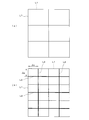
- (A), (b) is a figure which shows an exposure pattern.
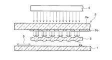
- FIG. 1 is a schematic view showing an exposure apparatus according to an embodiment of the present invention
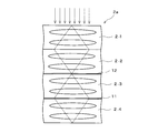
- FIG. 2 is a longitudinal sectional view showing a part of the same microlens array
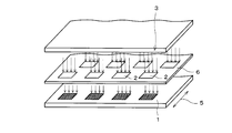
- FIG. 3 is a diagram in which a plurality of microlens arrays are arranged.
- FIG. 4 is a diagram showing the microlens
- FIGS. 5A and 5B are diagrams showing the diaphragm
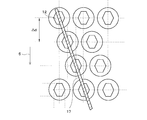
- FIG. 6 is a plan view showing the arrangement of the hexagonal field diaphragm of the microlens.
- 7 is a perspective view showing an exposure apparatus according to an embodiment of the present invention
- FIG. 8 is a plan view showing a method for detecting an exposure image by a CCD camera
- FIGS. 9A and 9B are views showing exposure patterns. .
- the exposure light emitted from the exposure light source 4 is guided to the mask 3 through an optical system 21 including a plane mirror, and the exposure light transmitted through the mask 3 is applied to the microlens array 2. Then, the pattern formed on the mask 3 is imaged on the substrate 1 by the microlens array 2.
- a dichroic mirror 22 is disposed on the optical path of the optical system 21, and observation light from the camera 23 is reflected by the dichroic mirror 22 and travels coaxially with the exposure light from the exposure light source 4 toward the mask 3.
- the observation light converges on the substrate 1 by the microlens array 2 and reflects the reference pattern already formed on the substrate 1, and the reflected light of the reference pattern is reflected by the microlens array 2, the mask 3 and the dichroic.
- the light enters the camera 23 via the mirror 22.
- the camera 23 detects the reflected light of the reference pattern and outputs this detection signal to the image processing unit 24.
- the image processing unit 24 performs image processing on the reference pattern detection signal to obtain a reference pattern detection image.
- the image signal of the reference pattern obtained by the image processing unit 24 is input to the control unit 25, and the control unit 25 detects the current position of the mask 3 (that is, the position of the exposure pattern to be exposed on the mask 3).
- a deviation from the position of the reference pattern is calculated, and an inclination angle of the microlens array 2 for eliminating the deviation amount is calculated.
- the control unit 25 outputs a signal corresponding to the inclination angle of the microlens array 2 to the actuator 20 including the piezoelectric elements 14 and 15 that drive the inclination of the microlens array 2.
- 14 and 15 drive the microlens array 2 by tilting based on this signal.
- the substrate 1 and the mask 3 can move together in a certain direction, and the microlens array 2, the exposure light source 4, and the optical system 21 are fixedly arranged. Then, when the substrate 1 and the mask 3 are moved in one direction, the exposure light is scanned on the substrate, and in the case of a so-called single-chip substrate in which one substrate is manufactured from a glass substrate, The entire surface of the substrate is exposed.
- a microlens array 2 configured by two-dimensionally arranging microlenses 2 a is disposed above a substrate 1 to be exposed such as a glass substrate.
- a mask 3 is disposed on the mask 3 and an exposure light source 4 is disposed above the mask 3.
- the mask 3 is formed with a light shielding film made of a Cr film 3b on the lower surface of the transparent substrate 3a, and the exposure light passes through the holes formed in the Cr film 3b and is converged on the substrate by the microlens array 2.
- the microlens array 2 and the exposure light source 4 are fixed, and the substrate 1 and the mask 3 are moved in the direction of the arrow 5 in synchronization, whereby exposure from the exposure light source 4 is performed.
- Light passes through the mask 3 and is scanned on the substrate 1 in the direction of arrow 5.
- the movement of the substrate 1 and the mask 3 is driven by a driving source of an appropriate moving device.
- the microlens array 2 and the exposure light source 4 may be moved while the substrate 1 and the mask 3 are fixed.
- microlens arrays 2 are arranged in two rows on the support substrate 6 in a direction perpendicular to the scanning direction 5, and four microlens arrays 2 are arranged in the scanning direction 5.
- three of the four microlens arrays 2 in the rear stage are respectively arranged between the four microlens arrays 2 in the front stage, and the two rows of microlens arrays 2 are arranged in a staggered manner. ing. Thereby, the entire region of the exposure region in the direction perpendicular to the scanning direction 5 on the substrate 1 is exposed by the two rows of microlens arrays 2.
- each microlens 2a of each microlens array 2 has, for example, a four-lens eight-lens configuration, and four microlens arrays 2-1, 2-2, 2-3, 2-4.
- Each microlens array 2-1 or the like is composed of two lenses.
- a hexagonal field stop 12 is disposed between the microlens array 2-2 and the microlens array 2-3, and an aperture stop 11 is disposed between the microlens array 2-3 and the microlens array 2-4.
- the hexagonal field stop 12 and the aperture stop 11 are provided for each microlens 2a, and the exposure area on the substrate is shaped into six corners for each microlens 2a.
- the hexagonal field stop 12 is formed as a hexagonal opening in the lens field area 10 of the microlens 2a
- the aperture stop 11 is formed as shown in FIG.
- a circular opening is formed in the lens visual field region 10 of the microlens 2a.
- FIG. 6 is a plan view showing an arrangement mode of each microlens 2a in each microlens array 2.
- FIG. 6 the arrangement of the microlenses 2a is shown as the position of the hexagonal field stop 12 of the microlenses 2a.
- the microlenses 2 a are sequentially shifted slightly in the lateral direction in the scanning direction 5.
- the hexagonal field stop 12 is divided into a central rectangular portion 12 a and triangular portions 12 b and 12 c on both sides when viewed in the scanning direction 5. As shown in FIG.
- the fourth row of microlenses 2 a are arranged at the same position as the first row of microlenses 2 a in the direction perpendicular to the scan direction 5.
- the line segments (shown by broken lines in the figure) connecting the respective corners of the hexagon of the hexagonal field stop 12 in the scanning direction 5 are equidistant, for example, 0.03 mm
- three rows of hexagons In the field stop 12 when the area of the triangular portion 12b of the two adjacent hexagonal field stops 12 and the area of the triangular portion 12c are added, the total area of the two triangular portions 12b and 12c overlapping in the scanning direction 5 is as follows.
- the area of the central rectangular portion 12a is the same.
- microlenses 2a in an integer multiple of 3 are arranged in the scanning direction 5, so that the substrate can be exposed with a uniform amount of light over the entire area by one scan. Will receive.
- the line segments (indicated by broken lines in the figure) that connect the respective corners of the hexagon of the hexagonal field stop 12 in the scanning direction 5 do not necessarily have to be equally spaced.
- the width of the rectangular portion 12a at the center of the hexagonal field stop 12 may be different from the height of the triangular portions 12b and 12c.
- the total area obtained by adding the areas of the two triangular portions 12b and the triangular portion 12c overlapping in the scanning direction 5 is the area of the central rectangular portion 12a. May not be the same.
- the length of the line segment where the straight line passes through the hexagonal field stop 12 is set on this straight line. It is only necessary that the total length when added over all hexagonal field stops is uniform in the direction perpendicular to the scanning direction 5.
- microlens rows can be provided in units of four rows.
- the microlenses are arranged such that (the left triangle portion) and (the right triangle portion in the fourth row + 1 the left triangle portion in the first row) overlap each other in the scan direction 5.
- the substrate 1 is moved relative to the microlens array 2 while the exposure light is irradiated from the exposure light source 4, and the substrate is scanned with the exposure light.
- the substrate 1 is exposed to a uniform amount of light over the entire exposure target area of the substrate 1. That is, the substrate 1 is not subjected to spot-like exposure according to the position of the microlens 2a, but the region between the microlenses 2a in one row is exposed by the microlenses 2a in the other row, and the substrate 1 is As in the case of receiving planar exposure, uniform exposure is performed over the entire area to be exposed.
- the pattern projected on the substrate 1 is determined not by the shapes of the hexagonal field stop 12 and the aperture stop 13 of the microlens 2 a but by the mask pattern (exposure pattern) formed in the hole of the light shielding film 3 b of the mask 3. It is a pattern.
- the microlens array 2 is arranged on the support plate 6 in two rows of the microlens array 2 b and the microlens array 2 c so as to form a row in a direction perpendicular to the scanning direction 5.
- the microlens array 2b and the microlens array 2c are arranged so as to be shifted from each other in the scanning direction 5.
- the microlens array 2 is disposed in a hole 6 a provided in the support plate 6, and each hole 6 a has a size corresponding to the outer shape of each microlens array 2. have.
- the microlens array 2 is arranged so that adjacent microlens arrays 2 (the microlens array 2b and the microlens array 2c) are close to each other in the direction orthogonal to the scanning direction 5.
- the portion of the support plate 6 between the microlens arrays 2 adjacent to each other in the direction orthogonal to the scan direction 5 is extremely thin, and the end of the microlens array 2 in the direction orthogonal to the scan direction 5 is this end.
- the distance between the microlenses 2a and the edge is shorter than 1/2 of the arrangement pitch of the microlenses 2a. Therefore, as shown in FIG.
- each microlens array 2 is connected between the microlenses 2 a of all the microlens arrays 2 in the direction orthogonal to the scan direction 5 even if the microlens arrays 2 are continuous in the direction orthogonal to the scan direction 5. Can be made the same interval. That is, the pitch in the direction orthogonal to the scanning direction 5 of the microlenses 2 a is constant for all the microlens arrays 2. In the scanning direction 5, one microlens array 2 is arranged, and the pitch of the microlenses 2a in the microlens array 2 is constant.
- the microlens array 2 can also be arranged on the support plate 6 so as to be separated from each other in both the scanning direction 5 and the direction orthogonal to the scanning direction 5 as shown in FIG.
- the microlens array 2 when viewed in the scanning direction 5, can be provided so that the ends overlap each other, and therefore, the end of each microlens array 2 in the direction orthogonal to the scanning direction 5. It is not necessary to shorten the distance between the microlens 2a and the edge of the microlens 2a so as to be less than 1 ⁇ 2 of the pitch of the microlens 2a. Further, the holes 6a of the support plate 6 do not need to have a short interval as shown in FIG.
- the microlens arrays 2 are arranged in a staggered manner in the direction orthogonal to the scanning direction 5, but the microlens arrays 2 are close to each other as shown in FIG. In this case, the microlens array 2 can be arranged in a straight line in the scanning direction 50.
- each microlens array 2b has, for example, two sides facing in the scanning direction 5, one supported by two piezoelectric elements 14a and 14b and the other by one piezoelectric element 15a.
- the microlens array 2c is supported by, for example, two sides facing the scanning direction 5, one supported by one piezoelectric element 14c and the other supported by two piezoelectric elements 15b and 15c. .
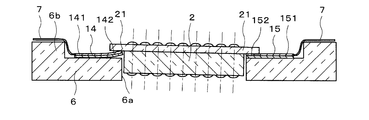
- holes 6a having a shape corresponding to the shape of the microlens array 2 are formed at the arrangement position of the microlens array 2 on the support plate 6 as described above. 2 is fitted in the hole 6a. In addition, the upper surface of the support plate 6 is notched around the hole 6a to form a step 6b.
- a piezoelectric element 14 (14a, 14a, 14b, 14c), 15 (15a, 15b, 15c) are arranged.
- the microlens array 2 is formed with a flange portion 21 extending in the horizontal direction at an upper portion thereof, and the flange portion 21 is positioned at a step 6b around the hole 6a of the support plate 6.
- the piezoelectric elements 14 and 15 have their base portions 141 and 151 fixed to the lower portion of the step 6 b of the support plate 6, and their tips 142 and 152 fixed to the lower surface of the flange portion 21 of the microlens array 2. Yes.
- the piezoelectric elements 14 and 15 are connected to an appropriate control device (not shown) via the lead wire 7, and the piezoelectric elements 14 and 15 are supplied with a drive voltage from the control device via the lead wire 7. As shown in FIG. That is, in FIG. 11, since the piezoelectric elements 14 and 15 are not deformed, the optical axis of the microlens array 2 is oriented in the vertical direction (perpendicular to the surface of the support plate 6).
- the left piezoelectric element 14 is deformed so that the tip 142 thereof faces upward, whereby the microlens array 2 is oriented in the direction in which the optical axis is inclined with respect to the vertical direction.
- the direction of the optical axis of the microlens array 2 can be adjusted by adjusting the voltage applied to the piezoelectric element, so if there is a misalignment between the reference pattern on the substrate and the exposure pattern.
- the positional deviation can be eliminated by detecting the positional deviation during exposure and adjusting the inclination angle of one or a plurality of microlens arrays.
- the support points by the piezoelectric elements 14 and 15 are not limited to the above-described three points, and four or more points may be provided. In this case, it is necessary to regulate the deformation amounts of four or more piezoelectric elements.
- the deformation amount of the piezoelectric elements 14 and 15 can be controlled by controlling the voltage applied to the piezoelectric elements 14 and 15, and the support is made at three points.
- the microlens array 2 can be tilted in an arbitrary direction.
- the camera 23 is a line CCD camera and detects an image in a one-dimensional line shape.
- FIG. 8 is a diagram showing the arrangement of the microlenses 2 a of the microlens array 2 and the detection area 17 of the line CCD camera 23.
- the hexagonal field stop 12 of the microlens 2a is adjacent to the nearest neighbor in the scanning direction 5 and is not parallel to the scanning direction 5, but is inclined.
- the linear detection region 17 is a straight line connecting the hexagonal field region 12 of the microlens 2a nearest to the scanning direction 5 from the hexagonal field region 12 of the corner microlens 2a.
- the detection area 17 is inclined with respect to the scanning direction 5 so as to coincide with each other.
- the detection region 17 of the line CCD camera 23 is, for example, from the microlens 2 a at the corner of the microlens array 2 to the other end in the width direction of the microlens array 2. That is, with respect to the direction perpendicular to the scanning direction 5, the hexagonal field region of the microlens 2 a located on the inclined line for the entire region in the width direction of the microlens array 2 from the corner portion of one end portion to the other end portion. Twelve images are detected.
- the scanning performance of the line CCD camera is 10 msec
- the moving speed of the substrate and the mask is, for example, 100 mm / sec.
- the mask moves 1 mm. Therefore, after detecting the image of the microlens 2 a at the corner of the microlens array 2 at one end of the line CCD camera 23, the width direction of the microlens array 2 at the other end of the line CCD camera 23.
- the image of the microlens 2a at the other end is an image 1 mm behind the position of the image of the microlens 2a at the corner. .
- the size in the width direction of the substrate and the mask is, for example, 1 m
- a displacement of 1 mm occurs per 1 m of the substrate. Therefore, between the adjacent microlenses 2a, the detected image is shifted in the scanning direction 5 by the amount obtained by dividing 1 mm by the number of microlenses 2a.
- the scan image by the line CCD camera 23 detects the image of the microlens 2a at the corner portion, and then detects the image of the microlens 2a obliquely forward in the substrate scanning direction 5.
- the images of the microlenses 2a arranged obliquely forward in the substrate scanning direction 5 are sequentially read. Accordingly, if the arrangement pitch of the microlenses 2a in the substrate scanning direction 5 is ⁇ d, the image signal read by the line CCD camera 23 in one scan is shifted by ⁇ d forward in the substrate scanning direction 5 by ⁇ d.
- the images of the lens 2a are read sequentially.
- this lens pitch ⁇ d is 150 ⁇ m
- the substrate moving speed is 100 mm / sec as described above
- this image is displayed as the micro lens 2a at the corner portion. It is an image at a position advanced by ⁇ d in the scan direction 5 of the substrate from the image at the position adjacent to the scan direction 5 of the image of FIG.
- an image at a position adjacent to the direction perpendicular to the scanning direction 5 of the image of the microlens 2a at the corner is obtained at that point in time from the next microlens 2a of the microlens 2a at the corner. This is an image detected by the second microlens 2a after 1.5 msec from the time.
- the image processing unit 24 obtains an image at a specific point in time while the substrate is moving when performing the above-described correction processing related to the time delay and the position adjustment from the acquisition signal of the line CCD camera 23. be able to.
- the first layer exposure pattern L1 reference pattern
- the image processing unit 24 performs image processing on the detection signal of the reference pattern L1, the reference pattern L1 shown in FIG. The detected image is obtained.
- the control unit 25 Based on the image detection signal of the image-processed pattern L1, the control unit 25 determines the reference position of the first layer pattern L1 and the reference position of the exposure pattern L2 formed on the mask 3 and to be exposed as the second layer pattern L2. And the inclination angle of the microlens array 2 for eliminating the amount of deviation is calculated. Then, the control unit 25 outputs a signal corresponding to the inclination angle of the microlens array 2 to the actuator 20 including the piezoelectric elements 14 and 15 that drive the inclination of the microlens array 2. 14 and 15) drive the microlens array by tilting based on this signal.
- the actuator 20 (piezoelectric elements 14 and 15) adjusts the voltage applied to the piezoelectric elements 14 and 15 based on the inclination angle of the microlens array 2 so that the microlens array 2 has a predetermined inclination angle. To drive.
- FIG. 13 is a diagram showing the relationship between the exposure light and the substrate 1 when the inclination angle of the microlens array 2 is gradually increased with respect to the adjacent microlens array 2.
- the incident angle of the exposure light with respect to the substrate 1 gradually decreases from 90 ° (becomes an acute angle).
- the distances b1, b2, b3 of the exposure regions between the adjacent microlens arrays 2 are gradually increased, and the inclination angle is the largest with respect to the pattern of the end portion (reference point) of the horizontally arranged microlens array 2.
- the pattern at the position farthest from the reference point of the large microlens array 2 is farther from the reference point than the exposure position when all the microlens arrays 2 are horizontal.
- the exposure position on the substrate can be adjusted and the exposure area on the substrate can be enlarged simply by gradually increasing the inclination angle of the microlens array 2 arranged in a row.
- the microlens array 2 may be inclined in the reverse direction.
- the substrate 1 is carried into a predetermined exposure position of the exposure apparatus.
- a pattern L1 as shown in FIG. 9A is exposed on the substrate 1 as a reference pattern.
- the reference pattern L1 is a first layer pattern, and the second layer pattern to the fourth layer pattern are exposed in the exposure apparatus on the basis of the first layer pattern, for example, a five layer pattern is overlaid and exposed.
- the exposure pattern in the overexposure shifts from the lower layer pattern. Therefore, the substrate 1 that has been loaded is scanned with the mask 3 together with the microlens array 2, and an image on the substrate 1 is detected by the line CCD camera 23.
- the line CCD camera 23 is a one-dimensional sensor, and is installed so as to detect a region inclined with respect to the substrate scanning direction 5 as shown in FIG. As described above, the detection region 17 of the line CCD camera 23 is not set in a direction perpendicular to the substrate scanning direction 5 but is inclined in this direction.
- the detection region 17 is arranged to be inclined so as to pass through the hexagonal field stop 12 of the microlens array 2 that is closest to the scanning direction 5 in the vicinity.
- the correction based on the delay time due to the inclination of the detection region 17 and the correction based on the time delay of one scan time of the CCD sensor are performed by image processing.
- the image on the substrate 1 can be detected using the detected image of the microlens 2a at the corner as a reference. That is, the image processing unit 24 obtains the first layer pattern L1 on the substrate 1 shown in FIG. 9A based on the detection signal of the camera 23.
- the control unit 25 exposes the second layer pattern L2 on the substrate. That is, the substrate 1 and the mask 3 are moved together with respect to the microlens array 2 and the light source, and the exposure pattern L2 formed on the mask 3 is superimposed and exposed on the first layer pattern L1.
- the second layer pattern L2 can be formed at a position separated from the corner portion serving as the reference of the first layer pattern L1 by the design values ⁇ x and ⁇ y.
- the eight microlens arrays 2 expose the entire exposure region in the direction perpendicular to the scanning direction 5 of the substrate 1 with a uniform amount of light. Then, when the substrate 1 and the mask 3 are scanned with respect to the microlens array 2 in the scanning direction 5, the exposure area on the entire surface of the substrate 1 is exposed with a uniform amount of light. Thereby, the mask pattern formed on the mask 3 forms an image on the substrate 1.
- the actuator 20 supplies voltage to the piezoelectric elements 14 and 15 to tilt the microlens array 2 so that the reference position of the exposure pattern L2 of the mask 3 matches the reference position of the first layer pattern L1.
- the incident angle of exposure light with respect to the substrate 1 is adjusted. For example, as shown in FIG. 13, when four microlens arrays 2 arranged in the direction perpendicular to the substrate scanning direction are inclined so that the inclination angle gradually increases, one microlens array is formed on the substrate 1.
- the inclination angle of the exposure light with respect to the substrate by each microlens 2a of the lens array 2 does not change, the exposure angle changes between the adjacent microlens arrays 2, and with respect to the horizontal microlens array 2 at the right end of FIG.
- the inclination of the exposure light from the microlens array 2 with respect to the substrate increases toward the left side.
- the mask pattern (indicated by ⁇ in the figure) of the mask 3 projected from each microlens array 2 onto the substrate 1 is projected onto the area a for each microlens array 2.
- the inclination angle of the exposure light is different for each microlens array 2, but the exposure area a is substantially the same size for each microlens array 2 because the inclination angle itself is extremely small.
- the mask pattern intervals b1, b2, b3 are gradually increased.
- the exposure area of the leftmost microlens array 2 in FIG. 13 with respect to the substrate is shifted to the left side compared to when all the microlens arrays 2 are horizontal.
- difference of the 1st layer pattern L1 and the 2nd layer pattern L2 can be eliminated.
- ⁇ x and ⁇ y are 70 ⁇ m
- the microlens array 2 on the left side is slightly inclined (about 1/1000 of several degrees) with respect to the rightmost microlens array 2, the exposure position is shifted by about 1 ⁇ m. Can do. Therefore, the pattern with a spacing of 70 ⁇ m can be shifted by 1 ⁇ m simply by tilting the microlens array 2 at a very small angle. Note that the method of tilting the microlens array 2 for eliminating the pattern displacement is not limited to that shown in FIG.
- the exposure position can be aligned with the exposure pattern in the lower layer. That is, in the present embodiment, the positional deviation between the lower layer pattern and the exposure pattern can be corrected by tilting the microlens array during the exposure in the exposure apparatus, and the positional deviation is corrected in real time to achieve high accuracy. Multiple exposures can be performed.
- the exposure light various kinds of light such as pulsed laser light or continuous light such as a mercury lamp can be used.
- the line CCD camera 23 uses a light irradiation unit that irradiates the substrate and a line CCD sensor that detects reflected light, and the substrate is irradiated with observation light from the camera 23 by the dichroic mirror 22.
- Light may be irradiated from below the substrate, and an image of the first layer exposure pattern formed on the substrate may be input to the line CCD sensor and detected.
- the image on the substrate is not limited to being detected by the line CCD sensor, and the image on the substrate can also be detected by a two-dimensional sensor.
- the present invention is not limited to the above embodiment.
- the line sensor of the line CCD camera 23 is arranged so that the detection region 17 is inclined with respect to the scan direction 5, thereby performing image processing, thereby An image in the hexagonal field stop 12 that is continuous without interruption is detected in the whole area in the direction perpendicular to 5, but the line sensors are arranged in a direction perpendicular to the scanning direction 5, and three lines of the line sensors are provided.
- a plurality of microlens arrays for projecting an erecting equal-magnification image of the mask exposure pattern onto the substrate are used, and the mask exposure pattern is formed on the substrate by adjusting the inclination angle of these microlens arrays.
- the magnification of the image when projected onto it can be adjusted.
- the positional deviation between the exposure pattern of the mask and the reference pattern on the substrate can be eliminated by adjusting the inclination angle of the microlens array. For this reason, this invention can expand the application object of the scanning exposure apparatus using a micro lens array, and its industrial utility value is high.
- Substrate 2 Microlens array 2a: Microlenses 2-1 to 2-4: (Configuration) Microlens array 3: Mask 3a: Transparent substrate 3b: Cr film 4: Exposure light source 5: Scanning direction 6: Support substrate 11 Aperture stop 12: Hexagon field stop 12a: Rectangular portion 12b, 12c: Triangular portion 14 (14a, 14b, 14c), 15 (15a, 15b, 15c): Piezoelectric element 17: Detection region 20: Actuator 21: Optical system 22: Dichroic mirror 23: Line CCD camera 24: Image processing unit 25: Control unit
Landscapes
- Physics & Mathematics (AREA)
- General Physics & Mathematics (AREA)
- Optics & Photonics (AREA)
- Exposure And Positioning Against Photoresist Photosensitive Materials (AREA)
- Exposure Of Semiconductors, Excluding Electron Or Ion Beam Exposure (AREA)
- Lenses (AREA)
Abstract
Description
2:マイクロレンズアレイ
2a:マイクロレンズ
2-1~2-4:(構成)マイクロレンズアレイ
3:マスク
3a:透明基板
3b:Cr膜
4:露光光源
5:スキャン方向
6:支持基板
11:開口絞り
12:6角視野絞り
12a:矩形部分
12b、12c:三角形部分
14(14a、14b、14c),15(15a、15b、15c):圧電素子
17:検出領域
20:アクチュエータ
21:光学系
22:ダイクロイックミラー
23:ラインCCDカメラ
24:画像処理部
25:制御部
Claims (4)
- 露光すべき基板の上方に配置され、マイクロレンズが2次元的に配置された複数個のマイクロレンズアレイと、このマイクロレンズアレイを傾斜可能に支持する支持基板と、前記各マイクロレンズアレイを前記支持基板に対して傾動駆動する駆動部材と、このマイクロレンズアレイの上方に配置され所定の露光パターンが形成されたマスクと、このマスクに対して露光光を照射する露光光源と、前記マイクロレンズアレイと前記基板及び前記マスクとを相対的に一方向に移動させる移動装置と、前記基板の画像を検出する画像検出部と、この画像の検出信号を基に画像処理して基板上に形成されている基準パターンを得る画像処理部と、この基準パターンと露光しようとする前記マスクの露光パターンとの間のずれを演算して前記基準パターンと前記露光パターンとのずれを解消するように前記駆動部材を介して前記マイクロレンズアレイを傾動させる制御部と、を有し、前記複数個のマイクロレンズアレイを基板の面に平行の方向から傾斜させることにより、基板上の露光位置を調整して、露光パターンを前記基準パターンに一致させることを特徴とするマイクロレンズアレイを使用したスキャン露光装置。
- 前記画像検出部は、画像を線状に検出するラインセンサであり、このラインセンサはその検出領域が前記一方向に対して鋭角をなすように傾斜して配置されており、1本のラインセンサで複数列のマイクロレンズ内の画像を検出することを特徴とする請求項1に記載のマイクロレンズアレイを使用したスキャン露光装置。
- 前記画像検出部は、画像を線状に検出する複数個のラインセンサであり、この複数個のラインセンサはその検出領域が前記一方向に対して直交する方向に配置されており、複数個のラインセンサの全体で複数列のマイクロレンズ内の画像を検出することを特徴とする請求項1に記載のマイクロレンズアレイを使用したスキャン露光装置。
- 前記マイクロレンズは、前記マスクの露光パターンの正立等倍像を前記基板上に投影することを特徴とする請求項1乃至3のいずれか1項に記載のマイクロレンズアレイを使用したスキャン露光装置。
Priority Applications (3)
| Application Number | Priority Date | Filing Date | Title |
|---|---|---|---|
| CN201180048221.0A CN103140804B (zh) | 2010-10-05 | 2011-09-12 | 使用微透镜阵列的扫描曝光装置 |
| US13/877,653 US9086514B2 (en) | 2010-10-05 | 2011-09-12 | Scanning exposure apparatus using microlens array |
| KR1020137011498A KR101869116B1 (ko) | 2010-10-05 | 2011-09-12 | 마이크로 렌즈 어레이를 사용한 스캔 노광 장치 |
Applications Claiming Priority (2)
| Application Number | Priority Date | Filing Date | Title |
|---|---|---|---|
| JP2010-225971 | 2010-10-05 | ||
| JP2010225971A JP5515119B2 (ja) | 2010-10-05 | 2010-10-05 | マイクロレンズアレイを使用したスキャン露光装置 |
Publications (1)
| Publication Number | Publication Date |
|---|---|
| WO2012046540A1 true WO2012046540A1 (ja) | 2012-04-12 |
Family
ID=45927537
Family Applications (1)
| Application Number | Title | Priority Date | Filing Date |
|---|---|---|---|
| PCT/JP2011/070735 Ceased WO2012046540A1 (ja) | 2010-10-05 | 2011-09-12 | マイクロレンズアレイを使用したスキャン露光装置 |
Country Status (6)
| Country | Link |
|---|---|
| US (1) | US9086514B2 (ja) |
| JP (1) | JP5515119B2 (ja) |
| KR (1) | KR101869116B1 (ja) |
| CN (1) | CN103140804B (ja) |
| TW (1) | TWI546630B (ja) |
| WO (1) | WO2012046540A1 (ja) |
Cited By (1)
| Publication number | Priority date | Publication date | Assignee | Title |
|---|---|---|---|---|
| WO2013176178A1 (ja) * | 2012-05-22 | 2013-11-28 | 株式会社ニコン | 露光装置、露光方法及びデバイス製造方法 |
Families Citing this family (9)
| Publication number | Priority date | Publication date | Assignee | Title |
|---|---|---|---|---|
| JP3361891B2 (ja) | 1994-07-01 | 2003-01-07 | オリジン電気株式会社 | 多段倍電圧整流回路の組立方法 |
| JP6283798B2 (ja) * | 2013-07-01 | 2018-02-28 | 株式会社ブイ・テクノロジー | 露光装置および照明ユニット |
| CN104865801B (zh) * | 2015-06-01 | 2017-03-01 | 京东方科技集团股份有限公司 | 曝光装置 |
| KR101704580B1 (ko) * | 2015-08-31 | 2017-02-08 | 포항공과대학교 산학협력단 | 집광렌즈 및 이를 이용한 리소그래피 장치 |
| CN105611173A (zh) * | 2016-02-26 | 2016-05-25 | 广东欧珀移动通信有限公司 | 终端、成像装置、交互系统、其控制方法及控制装置 |
| DE102017106831A1 (de) * | 2017-03-30 | 2018-10-04 | Sick Ag | Kamera und Verfahren zur Erfassung von relativ zu der Kamera in einer Förderrichtung bewegten Objekten |
| US11543654B2 (en) * | 2020-09-16 | 2023-01-03 | Aac Optics Solutions Pte. Ltd. | Lens module and system for producing image having lens module |
| CN112415736B (zh) * | 2020-11-24 | 2023-06-06 | 深圳技术大学 | 光场光学显微镜及光场光学显微系统 |
| CN119717089B (zh) * | 2025-02-28 | 2025-05-30 | 泉州信息工程学院 | 制备微透镜球面阵列的方法及系统 |
Citations (5)
| Publication number | Priority date | Publication date | Assignee | Title |
|---|---|---|---|---|
| JP2001500628A (ja) * | 1996-02-28 | 2001-01-16 | ケニス シー ジョンソン | マイクロリトグラフィ用マイクロレンズスキャナ及び広フィールド共焦顕微鏡 |
| WO2006137486A1 (ja) * | 2005-06-23 | 2006-12-28 | Fujifilm Corporation | 画像露光装置 |
| JP2007052214A (ja) * | 2005-08-17 | 2007-03-01 | Nikon Corp | 走査型露光装置及びマイクロデバイスの製造方法 |
| JP2008292916A (ja) * | 2007-05-28 | 2008-12-04 | Fujifilm Corp | 画像露光装置及びマイクロレンズユニット並びにその製造方法 |
| JP2009055060A (ja) * | 2004-04-30 | 2009-03-12 | Asml Netherlands Bv | リソグラフィ装置及びデバイス製造方法 |
Family Cites Families (6)
| Publication number | Priority date | Publication date | Assignee | Title |
|---|---|---|---|---|
| JPH09244255A (ja) * | 1996-03-13 | 1997-09-19 | Nikon Corp | 液晶用露光装置 |
| US6639201B2 (en) * | 2001-11-07 | 2003-10-28 | Applied Materials, Inc. | Spot grid array imaging system |
| US7459709B2 (en) * | 2003-08-27 | 2008-12-02 | Koninklijke Philips Electronics N.V. | Method of forming optical images, a control circuit for use with this method, apparatus for carrying out said method and process for manufacturing a device using said method |
| TW200602814A (en) | 2004-03-29 | 2006-01-16 | Fuji Photo Film Co Ltd | Exposure device |
| US7274029B2 (en) | 2004-12-28 | 2007-09-25 | Asml Netherlands B.V. | Lithographic apparatus and device manufacturing method |
| JP2007183363A (ja) * | 2006-01-05 | 2007-07-19 | Hitachi Maxell Ltd | マザー基板、このマザー基板の製造方法およびマイクロレンズアレイ基板の製造方法 |
-
2010
- 2010-10-05 JP JP2010225971A patent/JP5515119B2/ja active Active
-
2011
- 2011-09-12 CN CN201180048221.0A patent/CN103140804B/zh not_active Expired - Fee Related
- 2011-09-12 KR KR1020137011498A patent/KR101869116B1/ko not_active Expired - Fee Related
- 2011-09-12 WO PCT/JP2011/070735 patent/WO2012046540A1/ja not_active Ceased
- 2011-09-12 US US13/877,653 patent/US9086514B2/en not_active Expired - Fee Related
- 2011-10-03 TW TW100135781A patent/TWI546630B/zh not_active IP Right Cessation
Patent Citations (5)
| Publication number | Priority date | Publication date | Assignee | Title |
|---|---|---|---|---|
| JP2001500628A (ja) * | 1996-02-28 | 2001-01-16 | ケニス シー ジョンソン | マイクロリトグラフィ用マイクロレンズスキャナ及び広フィールド共焦顕微鏡 |
| JP2009055060A (ja) * | 2004-04-30 | 2009-03-12 | Asml Netherlands Bv | リソグラフィ装置及びデバイス製造方法 |
| WO2006137486A1 (ja) * | 2005-06-23 | 2006-12-28 | Fujifilm Corporation | 画像露光装置 |
| JP2007052214A (ja) * | 2005-08-17 | 2007-03-01 | Nikon Corp | 走査型露光装置及びマイクロデバイスの製造方法 |
| JP2008292916A (ja) * | 2007-05-28 | 2008-12-04 | Fujifilm Corp | 画像露光装置及びマイクロレンズユニット並びにその製造方法 |
Cited By (1)
| Publication number | Priority date | Publication date | Assignee | Title |
|---|---|---|---|---|
| WO2013176178A1 (ja) * | 2012-05-22 | 2013-11-28 | 株式会社ニコン | 露光装置、露光方法及びデバイス製造方法 |
Also Published As
| Publication number | Publication date |
|---|---|
| KR101869116B1 (ko) | 2018-06-19 |
| US9086514B2 (en) | 2015-07-21 |
| JP2012078721A (ja) | 2012-04-19 |
| TWI546630B (zh) | 2016-08-21 |
| KR20130105862A (ko) | 2013-09-26 |
| CN103140804A (zh) | 2013-06-05 |
| TW201222166A (en) | 2012-06-01 |
| CN103140804B (zh) | 2015-07-01 |
| US20130188161A1 (en) | 2013-07-25 |
| JP5515119B2 (ja) | 2014-06-11 |
Similar Documents
| Publication | Publication Date | Title |
|---|---|---|
| JP5515119B2 (ja) | マイクロレンズアレイを使用したスキャン露光装置 | |
| JP5515120B2 (ja) | マイクロレンズアレイを使用したスキャン露光装置 | |
| KR101941323B1 (ko) | 노광 장치용 얼라인먼트 장치 및 얼라인먼트 마크 | |
| TWI536114B (zh) | 使用微透鏡陣列之掃描曝光裝置 | |
| JP2009111430A (ja) | 露光装置 | |
| WO2013018572A1 (ja) | マイクロレンズアレイ及びそれを使用したスキャン露光装置 | |
| CN103907061B (zh) | 微透镜阵列以及使用该微透镜阵列的扫描曝光装置 | |
| JP2012128193A (ja) | マイクロレンズアレイ及びそれを使用したスキャン露光装置 | |
| JP5853343B2 (ja) | マイクロレンズアレイを使用したスキャン露光装置 | |
| JP5895275B2 (ja) | アライメントマーク及び露光装置 | |
| JP5704527B2 (ja) | マイクロレンズアレイを使用した露光装置 | |
| JP5874900B2 (ja) | 露光装置用のアライメント装置 |
Legal Events
| Date | Code | Title | Description |
|---|---|---|---|
| WWE | Wipo information: entry into national phase |
Ref document number: 201180048221.0 Country of ref document: CN |
|
| 121 | Ep: the epo has been informed by wipo that ep was designated in this application |
Ref document number: 11830473 Country of ref document: EP Kind code of ref document: A1 |
|
| WWE | Wipo information: entry into national phase |
Ref document number: 13877653 Country of ref document: US |
|
| NENP | Non-entry into the national phase |
Ref country code: DE |
|
| ENP | Entry into the national phase |
Ref document number: 20137011498 Country of ref document: KR Kind code of ref document: A |
|
| 122 | Ep: pct application non-entry in european phase |
Ref document number: 11830473 Country of ref document: EP Kind code of ref document: A1 |