WO2012017607A1 - 固体撮像装置、撮像装置 - Google Patents
固体撮像装置、撮像装置 Download PDFInfo
- Publication number
- WO2012017607A1 WO2012017607A1 PCT/JP2011/004045 JP2011004045W WO2012017607A1 WO 2012017607 A1 WO2012017607 A1 WO 2012017607A1 JP 2011004045 W JP2011004045 W JP 2011004045W WO 2012017607 A1 WO2012017607 A1 WO 2012017607A1
- Authority
- WO
- WIPO (PCT)
- Prior art keywords
- solid
- imaging device
- light
- state imaging
- pixel
- Prior art date
- Legal status (The legal status is an assumption and is not a legal conclusion. Google has not performed a legal analysis and makes no representation as to the accuracy of the status listed.)
- Ceased
Links
Images








Classifications
-
- H—ELECTRICITY
- H04—ELECTRIC COMMUNICATION TECHNIQUE
- H04N—PICTORIAL COMMUNICATION, e.g. TELEVISION
- H04N25/00—Circuitry of solid-state image sensors [SSIS]; Control thereof
-
- H—ELECTRICITY
- H04—ELECTRIC COMMUNICATION TECHNIQUE
- H04N—PICTORIAL COMMUNICATION, e.g. TELEVISION
- H04N25/00—Circuitry of solid-state image sensors [SSIS]; Control thereof
- H04N25/10—Circuitry of solid-state image sensors [SSIS]; Control thereof for transforming different wavelengths into image signals
- H04N25/11—Arrangement of colour filter arrays [CFA]; Filter mosaics
- H04N25/13—Arrangement of colour filter arrays [CFA]; Filter mosaics characterised by the spectral characteristics of the filter elements
- H04N25/134—Arrangement of colour filter arrays [CFA]; Filter mosaics characterised by the spectral characteristics of the filter elements based on three different wavelength filter elements
-
- H—ELECTRICITY
- H04—ELECTRIC COMMUNICATION TECHNIQUE
- H04N—PICTORIAL COMMUNICATION, e.g. TELEVISION
- H04N25/00—Circuitry of solid-state image sensors [SSIS]; Control thereof
- H04N25/50—Control of the SSIS exposure
- H04N25/57—Control of the dynamic range
- H04N25/58—Control of the dynamic range involving two or more exposures
- H04N25/581—Control of the dynamic range involving two or more exposures acquired simultaneously
- H04N25/585—Control of the dynamic range involving two or more exposures acquired simultaneously with pixels having different sensitivities within the sensor, e.g. fast or slow pixels or pixels having different sizes
-
- H—ELECTRICITY
- H04—ELECTRIC COMMUNICATION TECHNIQUE
- H04N—PICTORIAL COMMUNICATION, e.g. TELEVISION
- H04N25/00—Circuitry of solid-state image sensors [SSIS]; Control thereof
- H04N25/70—SSIS architectures; Circuits associated therewith
- H04N25/76—Addressed sensors, e.g. MOS or CMOS sensors
- H04N25/77—Pixel circuitry, e.g. memories, A/D converters, pixel amplifiers, shared circuits or shared components
-
- H—ELECTRICITY
- H10—SEMICONDUCTOR DEVICES; ELECTRIC SOLID-STATE DEVICES NOT OTHERWISE PROVIDED FOR
- H10F—INORGANIC SEMICONDUCTOR DEVICES SENSITIVE TO INFRARED RADIATION, LIGHT, ELECTROMAGNETIC RADIATION OF SHORTER WAVELENGTH OR CORPUSCULAR RADIATION
- H10F39/00—Integrated devices, or assemblies of multiple devices, comprising at least one element covered by group H10F30/00, e.g. radiation detectors comprising photodiode arrays
- H10F39/80—Constructional details of image sensors
- H10F39/804—Containers or encapsulations
-
- H—ELECTRICITY
- H10—SEMICONDUCTOR DEVICES; ELECTRIC SOLID-STATE DEVICES NOT OTHERWISE PROVIDED FOR
- H10F—INORGANIC SEMICONDUCTOR DEVICES SENSITIVE TO INFRARED RADIATION, LIGHT, ELECTROMAGNETIC RADIATION OF SHORTER WAVELENGTH OR CORPUSCULAR RADIATION
- H10F39/00—Integrated devices, or assemblies of multiple devices, comprising at least one element covered by group H10F30/00, e.g. radiation detectors comprising photodiode arrays
- H10F39/80—Constructional details of image sensors
- H10F39/806—Optical elements or arrangements associated with the image sensors
- H10F39/8067—Reflectors
-
- H—ELECTRICITY
- H10—SEMICONDUCTOR DEVICES; ELECTRIC SOLID-STATE DEVICES NOT OTHERWISE PROVIDED FOR
- H10F—INORGANIC SEMICONDUCTOR DEVICES SENSITIVE TO INFRARED RADIATION, LIGHT, ELECTROMAGNETIC RADIATION OF SHORTER WAVELENGTH OR CORPUSCULAR RADIATION
- H10F39/00—Integrated devices, or assemblies of multiple devices, comprising at least one element covered by group H10F30/00, e.g. radiation detectors comprising photodiode arrays
- H10F39/80—Constructional details of image sensors
- H10F39/811—Interconnections
-
- H—ELECTRICITY
- H10—SEMICONDUCTOR DEVICES; ELECTRIC SOLID-STATE DEVICES NOT OTHERWISE PROVIDED FOR
- H10F—INORGANIC SEMICONDUCTOR DEVICES SENSITIVE TO INFRARED RADIATION, LIGHT, ELECTROMAGNETIC RADIATION OF SHORTER WAVELENGTH OR CORPUSCULAR RADIATION
- H10F77/00—Constructional details of devices covered by this subclass
- H10F77/10—Semiconductor bodies
- H10F77/12—Active materials
Definitions
- the present invention relates to a solid-state imaging device and an imaging device mounted on a digital still camera or the like.
- an external ND (Neutral Density) filter that adjusts the amount of light according to the illuminance of the subject or shooting location and a mechanical mechanical aperture are used. Since it operates as a separate element, it is difficult to reduce the size of the camera. Therefore, the external ND filter and the mechanical mechanical diaphragm are not used particularly for small cameras such as a security digital camera and a mobile phone terminal camera.
- Patent Document 1 as a camera that does not use a mechanical diaphragm, a solid-state imaging device housed in the camera, a parallel imaging device arranged in parallel with the imaging surface of the solid-state imaging device, integrated into a package, and energized to transmit light.
- a solid-state imaging device provided with a light amount adjusting means for controlling the light intensity.
- FIG. 14 is a cross-sectional view of the structure of a conventional solid-state imaging device described in Patent Document 1.
- a light quantity adjustment unit 503 is disposed inside a CCD package 502 in which the imaging surface of a CCD (Charge Coupled Device) element 501 is bonded.
- the light amount adjustment unit 503 is a known electrochromic element formed by unitizing a glass plate 504, a transparent conductive film 505, an electrochromic film 506, and an electrolytic film 507 with a frame 503a.
- the electrochromic film 506 is colored gray by applying voltage from the terminal A and the terminal B, and shows a phenomenon that it is colorlessly erased by a reverse polarity direct current.
- the transmitted light intensity of the light amount adjustment unit 503 is adjusted.
- the solid-state imaging device 508 can reversibly change the light transmittance by applying a voltage by using an electrochromic element as a light amount adjusting unit. According to this configuration, it is possible to perform imaging with the light amount adjusted even under high illuminance. Furthermore, since the electrochromic element does not use a mechanical mechanism such as a motor but uses a thin film, the camera can be downsized.
- Patent Document 1 since the structure of the solid-state imaging device described in Patent Document 1 has only an effect of uniformly reducing the amount of light within the angle of view, it has a problem of reducing the dynamic range within the same angle of view. .
- the signal intensity of the low-brightness subject is restricted by limiting the amount of light transmission with a filter using the electrochromic element described in FIG. Decreases, and the deterioration of S / N is inevitable.
- the glass plate 504 for sealing the light amount adjustment unit 503 is provided on the optical axis separately from the CCD element 501. Therefore, there is a problem that a pseudo image or a pseudo signal called ghost or flare is generated due to multiple reflection between the surface of the CCD element 501 and the light amount adjustment unit 503, and the image quality is deteriorated.
- the present invention has been made in view of the above problems, and provides a solid-state imaging device capable of adjusting the amount of light without an aperture mechanism and capable of imaging with a wide dynamic range even under high illuminance.
- the purpose is to provide.
- a solid-state imaging device includes a solid-state imaging device having an imaging region in which pixel units each including a photoelectric conversion element formed on the surface of a semiconductor substrate are two-dimensionally arranged.
- An interlayer film made of a dielectric formed on the photoelectric conversion element, and on the interlayer film, corresponding to each pixel unit or each pixel block consisting of a plurality of pixel units.
- a formed optical attenuation filter whose light transmittance is changed by voltage application, and formed in the semiconductor substrate corresponding to the optical attenuation filter, for connecting or blocking a voltage application path to the optical attenuation filter The switching transistor is provided.
- the light attenuation filter capable of adjusting the transmittance is arranged for each pixel unit or pixel block, it is possible to set the exposure condition for each pixel unit or pixel block. Therefore, even if a high-luminance subject and a low-luminance subject are mixed within the angle of view, the amount of light transmission can be limited for each pixel unit or pixel block. A wide dynamic range that is not saturated with respect to the region can be realized.
- optical attenuation filter is laminated on the photoelectric conversion unit in units of pixel units or pixel blocks via an interlayer film made of a dielectric, it is possible to suppress ghosts and flares due to multiple reflections. It becomes.
- the light attenuation filter includes a lower transparent electrode laminated on the dielectric film, a solid electrolyte layer and an active material layer laminated on the lower transparent electrode, and the solid electrolyte layer and the active material layer.
- An upper transparent electrode stacked on an upper layer of the material layer, and the solid electrolyte layer is made of an insulating dielectric, and ions are inserted by applying a voltage to the lower transparent electrode and the upper transparent electrode.
- the active material layer is a material whose light absorption spectrum changes with insertion and emission of the ions due to voltage application.
- the active material layer is preferably an amorphous film made of WO 3 , MoO 3 or IrO 2 .
- the solid electrolyte layer is made of at least one of ZrO 2 , Ta 2 O 5 , Cr 2 O 3 , V 2 O 5 , SiO 2 , Nb 2 O 5 and HfO 2 and contains hydrogen. May be.
- the solid electrolyte layer may be made of one of oxides of zirconia, tantalum, chromium, vanadium, niobium, and hafnium containing at least one of Li, Na, and Ag.
- the non-volatile element Li, Na, or Ag is used as the ion conduction medium, ion introduction into the solid electrolyte can be quantitatively performed, so that variation in the transmittance of the light attenuation filter is reduced and the transmittance is reduced. More accurate control. Therefore, it is possible to provide a solid-state imaging device having a high yield, high definition, and a wide dynamic range.
- the light attenuating filter further includes a thin film insulating layer made of an insulator between the solid electrolyte layer and the active material layer, and the insulator is one of SiO 2 , SiON, and SiN. It may be.
- the leakage current of the electrochromic element can be suppressed by inserting the thin film insulating layer between the solid electrolyte layer and the active material layer. Therefore, it is possible to suppress variation in transmittance within the surface of the light attenuating filter, ensure reproducibility of the transmittance, and maintain the transmittance for a long time. Therefore, it is possible to provide a solid-state imaging device equipped with a high-performance optical attenuation filter with a high yield.
- the solid-state imaging device is preferably installed in a hermetically sealed package filled with N 2 or a rare gas.
- an imaging device includes a solid-state imaging device according to any one of the above-described aspects of the solid-state imaging device and a light amount incident on the imaging region.
- a signal processing device for adjusting wherein the signal processing device determines in advance whether or not the luminance signal output from the pixel unit is saturated before imaging exposure, and the determination unit When it is determined that the luminance signal is saturated, the light attenuating filter is set by setting an applied voltage to the light attenuating filter before the imaging exposure so that the luminance signal during the imaging exposure is equal to or less than the saturation signal.
- a transmittance control unit for electrically controlling the transmittance of the light.
- the light transmission amount at the time of imaging exposure is controlled by the light attenuation filter based on the luminance signal saturation determination executed in advance, so that downsizing can be realized and imaging capable of imaging even under high illuminance is possible.
- An apparatus can be provided.
- the solid-state imaging device includes the light attenuation filter for each pixel block configured by a pixel portion of 2 rows and 2 columns, and the signal processing device is further configured in advance.
- a specifying unit that specifies a region that outputs a saturation signal from the acquired luminance signal intensity distribution of the imaging region; and the transmittance control unit is configured to perform the imaging exposure of the pixel block included in the region specified by the specifying unit.
- the solid-state imaging device includes a pixel block including a pixel unit of 2 rows and 2 columns, and the pixel block includes a G1 pixel unit that obtains a green signal;
- a Bayer array is formed of a G2 pixel unit, an R pixel unit that obtains a red signal, and a B pixel unit that obtains a blue signal, and the light attenuation filter is disposed above the G1 pixel unit and the G2 pixel unit.
- the determination unit determines in advance before imaging exposure whether the luminance signals output from the G1 pixel unit and the G2 pixel unit are saturated, and the transmittance control unit When the luminance signal is determined to be saturated by the unit, the voltage applied to the light attenuation filter is set before the imaging exposure so that the luminance signal during the imaging exposure is equal to or lower than the saturation signal.
- Light attenuation filter Over rate may be electrically controlled.
- the light attenuation filter only for the green signal with the highest visibility, the drive area of the light attenuation filter is reduced, the drive power can be reduced, and the red and blue sensitivities with low visibility are maintained. Since high-intensity imaging is possible, it is possible to provide a solid-state imaging device that realizes a wide dynamic range with low power consumption.
- the solid-state imaging device of the present invention it is possible to reduce the thickness and reduce the size by forming a light attenuating filter made of an electrochromic element for each pixel unit or pixel block. Further, according to the imaging device of the present invention, it is possible to control the light transmittance according to the luminance in the imaging region by providing a signal processing device that adjusts the transmittance of the light attenuation filter by determining the saturation signal. It becomes. Therefore, it is possible to provide a solid-state imaging device capable of realizing a wide dynamic range and capable of imaging even under high illuminance.
- FIG. 1 is a functional block diagram showing the configuration of the imaging apparatus according to Embodiment 1 of the present invention.
- FIG. 2 is a circuit configuration diagram of a pixel block included in the solid-state imaging device according to Embodiment 1 of the present invention.
- FIG. 3A is an operation flowchart of the signal processing apparatus according to Embodiment 1 of the present invention.
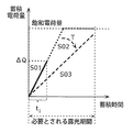
- FIG. 3B is a graph showing the relationship between the accumulated charge amount and accumulation time of the photoelectric conversion unit.
- FIG. 4 is an example of a schematic cross-sectional view of a unit pixel included in the solid-state imaging device according to Embodiment 1 of the present invention.
- FIG. 1 is a functional block diagram showing the configuration of the imaging apparatus according to Embodiment 1 of the present invention.
- FIG. 2 is a circuit configuration diagram of a pixel block included in the solid-state imaging device according to Embodiment 1 of the present invention.
- FIG. 3A is an operation flowchart of the signal processing apparatus according to Embod
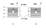
- FIG. 5 is a cross-sectional view of the structure of the optical attenuating filter according to Embodiment 1 of the present invention and a diagram illustrating the driving principle.
- FIG. 6 is a diagram showing a light transmission spectrum of WO 3 before and after hydrogen introduction.
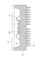
- FIG. 7 is an example of a structural cross-sectional view of a solid-state imaging device showing a modification according to Embodiment 1 of the present invention.
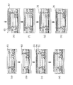
- FIG. 8 is a process cross-sectional view of the optical attenuation filter included in the solid-state imaging device according to Embodiment 1 of the present invention.
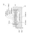
- FIG. 9 is a schematic cross-sectional view illustrating a mounted state of the solid-state imaging device according to Embodiment 1 of the present invention.
- FIG. 10 is a schematic diagram of an imaging region of the solid-state imaging device according to Embodiment 2 of the present invention.
- FIG. 11A is an operation flowchart of the signal processing apparatus according to Embodiment 2 of the present invention.
- FIG. 11B is a graph showing the adjustment operation of the accumulated charge amount of the photoelectric conversion unit by the signal processing device.
- FIG. 12 is a schematic diagram of an imaging region of the solid-state imaging device according to Embodiment 3 of the present invention.
- FIG. 13 is a structural sectional view of the optical attenuation filter 36 according to the fourth embodiment of the present invention and a diagram showing the driving principle.
- FIG. 14 is a sectional view of the structure of a conventional solid-state imaging device described in Patent Document 1.
- FIG. 1 is a functional block diagram showing the configuration of the imaging apparatus according to Embodiment 1 of the present invention.
- An imaging device 200 illustrated in the figure is a digital camera including a solid-state imaging device 100, a lens 201, a drive circuit 202, a signal processing device 203, and an external interface unit 204.
- the signal processing device 203 drives the solid-state imaging device 100 through the driving circuit 202, takes in an output signal from the solid-state imaging device 100, and outputs the internally processed signal to the outside via the external interface unit 204.
- the solid-state imaging device 100 has an active light attenuation filter for attenuating the amount of incident light in units of pixel units or pixel blocks, and the signal processing device 203 sets the attenuation rate of the light attenuation filter in units of pixels or pixels in advance. By setting in block units, it is possible to adjust the amount of light incident on the imaging region.
- FIG. 2 is a circuit configuration diagram of a pixel block included in the solid-state imaging device according to Embodiment 1 of the present invention.
- the solid-state imaging device 100 shown in the figure includes an imaging region 2 in which unit pixels 1 each having a photoelectric conversion unit 11 that is a photodiode are two-dimensionally arranged, a horizontal shift register 3 for selecting a pixel signal, and A vertical shift register 4 and an output terminal 5 for providing a signal from the selected unit pixel 1 to the outside are provided.
- the imaging area 2 includes a plurality of unit pixels 1.
- the unit pixel 1 includes a photoelectric conversion unit 11, a transfer transistor 12, a reset transistor 13, an amplification transistor 14, and a selection transistor 15.
- Each of the transfer transistor 12, the reset transistor 13, the amplification transistor 14, and the selection transistor 15 is configured by a MOS transistor.
- the solid-state imaging device 100 includes a light attenuation filter 16 and a selection transistor 17.
- the light attenuation filter 16 is formed on the incident light side of the imaging region 2.
- the selection transistor 17 is disposed between the voltage line 18 and the light attenuation filter 16.
- the gate of the selection transistor 17 is connected to the readout line 19 and switches between conduction and non-conduction between the voltage line 18 and the light attenuation filter 16 according to a control signal from the readout line 19.
- Both the positive potential and the negative potential can be selectively applied to the voltage line 18.
- a positive voltage is applied to the voltage attenuation line 16 by applying a positive voltage to the voltage line 18 and turning on the selection transistor 17.
- the conduction period of the selection transistor 17 that is, the period during which the positive voltage is applied to the light attenuation filter 16
- a desired transmittance of the light attenuation filter 16 can be obtained.
- the selection transistor 17 is turned off, and normal imaging driving is performed with the set transmittance.
- a negative voltage is applied to the voltage line 18 to turn on the selection transistor 17 and return the light attenuation filter 16 to its original state.
- the transmittance adjustment operation of the light attenuation filter 16 and the reset operation of the photoelectric conversion unit 11 are sequentially performed in time series with the imaging operation of the unit pixel 1, the photoelectric conversion unit before luminance signal saturation measurement and imaging operation described later is performed. It is possible to reset the charge accumulated in 11.
- the transmittance adjustment operation of the light attenuation filter 16, the imaging operation and the reset operation of the unit pixel 1 can be individually operated without installing a new signal line.
- the selection transistor 17 for controlling the voltage application to the optical attenuation filter 16 is provided.
- the selection transistor 17 can be made unnecessary by driving the voltage line 18 in a pulsed manner. is there.
- the readout line 19 may be turned off, and if the voltage line 18 is set to 0 V during the exposure period, the transmittance set by the transmittance adjustment operation. Does not change during exposure.
- a voltage is applied to the voltage line 18, but even if the transmittance of the light attenuation filter 16 changes at that time, it becomes a pseudo signal if charge has already been accumulated.
- the readout line 19 may be turned off again and the light attenuation filter 16 may be turned off after readout.
- a transistor for controlling voltage application to the light attenuation filter 16 is not necessary, and therefore the light attenuation filter 16 can be mounted on each pixel even for a fine pixel.
- the signal processing device 203 determines whether or not the luminance signal output from the pixel block including the unit pixel 1 or the plurality of unit pixels 1 is saturated before the imaging exposure, and the determination unit determines the luminance signal. Is determined to be saturated, the transmittance of the light attenuating filter 16 is set by setting the voltage applied to the light attenuating filter 16 before the image capturing exposure so that the luminance signal at the time of image capturing exposure is less than the saturation signal.
- a transmittance control unit that is electrically controlled.
- FIG. 3A is an operation flowchart of the signal processing apparatus according to Embodiment 1 of the present invention.
- FIG. 3B is a graph showing the relationship between the accumulated charge amount and the accumulation time of the photoelectric conversion unit.
- step S01 luminance signal saturation measurement is performed by the signal processing device 203 (step S01), and after the transmittance of the light attenuation filter 16 is decreased (step S02), the subject is imaged (step S03). That's it.
- the determination unit of the signal processing device 203 calculates ⁇ Q / t1 corresponding to the inclination of the graph shown in FIG. 3B from the accumulated charge amount ⁇ Q accumulated by the exposure in the period t1 as the luminance signal saturation measurement.
- the luminance signal in the exposure period required when the incident light is not attenuated by the light attenuation filter 16 is saturated, that is, whether the accumulated charge amount in the period reaches the saturated charge amount. judge.
- the signal processing device 203 sets a threshold for the luminance signal intensity in advance in the signal processing area.
- the transmittance control unit operates the light attenuation filter 16 to reduce ⁇ Q / t1 corresponding to the storage efficiency by the transmittance T to prevent saturation.
- the photoelectric conversion unit 11 determines whether the photoelectric conversion unit 11 has saturation illuminance or saturation luminance for shooting under high illuminance or a high brightness subject, and the light of the light attenuation filter 16 is not saturated. Transmittance can be controlled. Therefore, imaging under high illuminance is possible.
- the light transmission amount at the time of imaging exposure is controlled by the light attenuation filter 16 by the luminance signal saturation determination performed in advance by preliminary imaging, downsizing can be realized and imaging can be performed even under high illuminance. It becomes possible to provide an imaging device 200 that can be used.
- FIG. 4 is an example of a schematic cross-sectional view of a unit pixel included in the solid-state imaging device according to Embodiment 1 of the present invention.
- the unit pixel 1 shown in the figure includes a photoelectric conversion unit 11, a light attenuation filter 16, a semiconductor substrate 20, a gate and gate wiring 22, an interlayer film 24, a color filter 26, and a planarization film 27. , Microlenses 28 and wiring layers 57 and 59.
- the light attenuation filter 16 is disposed above the uppermost wiring layer 59 and below the color filter 26.
- the wiring material of the wiring layers 57 and 59 is, for example, AlCu. Also, the number of wiring layers is two layers of wiring layers 57 and 59.
- the light attenuation filter 16 includes transparent electrodes 31 and 32, an active material layer 33, and a solid electrolyte layer 34, and a laminated film of the active material layer 33 and the solid electrolyte layer 34 is sandwiched between the transparent electrodes 31 and 32. It has a capacitor structure.
- the transparent electrodes 31 and 32 are each electrically connected to the wiring layer 59, and the lower transparent electrode electrically connected to the selection transistor 17 (not shown) formed on the semiconductor substrate via the wiring layer 59. And the upper transparent electrode. As described above, the applied voltage of the light attenuation filter 16 is controlled by the conduction and non-conduction of the selection transistor 17.
- FIG. 5 is a structural sectional view of the optical attenuating filter according to the first embodiment of the present invention and a diagram showing a driving principle.
- the light attenuation filter 16 in the present embodiment uses an electrochromic element.
- An electrochromic element is a generic term for elements in which the absorption spectrum of a material changes when a voltage is applied, and the color changes.
- an element whose transmittance is changed by changing the orientation of liquid crystal molecules by an electric field, such as liquid crystal is one of the electrochromic elements.
- electrochromic devices using solid electrolytes that change the absorption spectrum due to redox reactions caused by ion migration in solids have no polarization dependence like liquid crystals, and there are also materials that exhibit unique spectra. Therefore, it is widely used for display elements.
- the state A shown in FIG. 5A indicates that the active material of the active material layer 33 is in an oxidized state by applying a positive voltage to the transparent electrode 32 on the active material layer 33 side. Show. Thereby, ions move from the active material layer 33 to the solid electrolyte layer 34, and at the same time, electrons are emitted from the active material layer 33 to the transparent electrode 32. In this state A, the light attenuation filter 16 is in a transparent state.
- the conduction ion is basically a cation
- the cation moves in the direction opposite to the direction of the electrons.
- a current corresponding to an oxidation-reduction current corresponding to the amount of ion movement from the active material enters and exits.
- the amount of movement of ions can be controlled by the voltage application time to the electrodes, whereby the amount of transmitted light can be controlled, and a solid-state imaging device capable of imaging even under high illuminance can be realized.
- the active material layer 33 constituting the light attenuation filter 16 is made of any one material of amorphous oxides represented by WO 3 , MoO 3 , and IrO 2 .
- the solid electrolyte layer 34 is made of at least one of oxide materials represented by ZrO 2 , Ta 2 O 5 , Cr 2 O 3 , V 2 O 5 , SiO 2 , Nb 2 O 5 , and HfO 2 .
- WO 3 is used as a constituent material of the active material layer 33 and Ta 2 O 5 is used as a constituent material of the solid electrolyte layer 34
- the combination of WO 3 and Ta 2 O 5 is one of the common combinations for electrochromic devices.
- an oxidation-reduction reaction accompanied by ion transfer occurs between WO 3 and Ta 2 O 5, and the electronic structure of WO 3 changes greatly. It is possible to control in steps between the transparent state and the colored state.
- WO 3 is a highly ionic oxide, and W in WO 3 exists in a state close to W 6+ in which valence electrons have been taken away by O. In this state, it is a transparent material having a band gap of about 3.8 eV. However, if hydrogen or an alkali metal is present here, they enter between W and O and give their own electrons to the W side. Causes a reduction reaction. This reduced electron occupies the d electron level of W and greatly contributes to light absorption.
- FIG. 6 is a diagram showing a light transmission spectrum of WO 3 before and after hydrogen introduction.
- HxWO 3 is a state in which hydrogen is introduced into WO 3 at a non-stoichiometric ratio. As shown in the figure, in the state without hydrogen (WO 3 ), it can be seen that the visible light region has a very high transparency.
- H x WO 3 into which hydrogen is introduced strong light absorption is observed from green to red. Even in the blue region where the light absorption is relatively small, the transmittance is reduced by about 40%, and since blue is originally a color with low visibility, it becomes a sufficient light attenuation filter for visible light.
- the active material layer 33 is preferably an amorphous film.
- WO 3 is a crystal
- the number of sites where ions such as hydrogen enter is reduced, and at the same time, the ion movement speed is reduced.
- an amorphous film is optimal for the present invention.
- amorphous WO 3 can be formed at a low temperature, it has a very high affinity with the silicon process.
- the solid electrolyte layer 34 uses a H + ion as a conductive ion, for loading and unloading the H + ions between the active material layer 33, a transparent material is moved in the storage and H + ions of H + ions is easy Desired. Further, since the conductive ions are driven by the electric field in the solid electrolyte layer 34 and the active material layer 33, the solid electrolyte layer 34 is required to have insulating properties. ZrO 2 , Ta 2 O 5 , Cr 2 O 3 , V 2 O 5 , SiO 2 , Nb 2 O 5 and HfO 2 are transparent oxide dielectrics with excellent insulating properties and contain H + ions.
- the present embodiment is the best mode for conducting H + ions.
- the device structure according to the first exemplary embodiment of the present invention includes an electrochromic element including a pair of active material layers 33 and a solid electrolyte layer 34 provided above the uppermost wiring layer 59 with an interlayer film therebetween. Therefore, a process for forming a light attenuating filter is required before forming a color filter. Details of the manufacturing process after the uppermost wiring layer will be described below.
- FIG. 7 is an example of a cross-sectional view of the structure of the solid-state imaging device showing a modification according to Embodiment 1 of the present invention.
- the solid-state imaging device 110 shown in the figure is a MOS image sensor.
- FIG. 8 is a process cross-sectional view of the optical attenuation filter included in the solid-state imaging device according to Embodiment 1 of the present invention.
- a diffusion region 52 is formed in the semiconductor substrate 20 by ion implantation.
- an imaging region 51 and a peripheral circuit region 50 of the pixel portion are formed on the semiconductor substrate 20.
- the transistor 54 is electrically isolated by the element isolation part 53.
- an interlayer film 56 made of an insulator such as BPSG (Boron Phosphorate Silicate Glass) is formed, planarized by CMP (Chemical Mechanical Polishing) or etch back, and then contact holes are formed by dry etching.
- the metal plug 55 is formed by a metal CVD method. With the metal plug 55 exposed, an aluminum film is formed by sputtering or the like, and patterning is performed by dry etching to produce the wiring layer 57. By repeating this process configuration, a multilayer wiring structure can be made.
- the transistor 54 corresponds to, for example, any of the transfer transistor 12, the reset transistor 13, the amplification transistor 14, and the selection transistors 15 and 17 illustrated in FIG.
- the interlayer film 24 made of an insulating dielectric is formed on the upper portion of the first wiring layer 57 to planarize the metal plug. After the formation, a second wiring layer 59 is formed.
- an interlayer film 61 made of an insulating dielectric is formed of BPSG and planarized using CMP.
- a metal plug 60 is formed. Here, the metal plug 60 is exposed.
- the transparent electrode 31, the solid electrolyte layer 34, and the active material layer 33 of the light attenuation filter 16 are stacked.
- the lower transparent electrode 31 is electrically connected to the metal plug 60. Since the light attenuating filter 16 basically needs to transmit light, the transparent electrode 31 uses ITO transparent to visible light.
- the film thickness of the transparent electrode 31 is, for example, 200 nm.
- the light attenuation filter 16 is provided above the two wiring layers 57 and 59.
- the pixel structure is not limited to this, and the light attenuation filter 16 is not limited to the first layer. It may be provided between the wiring layer 57 and the second wiring layer 59.
- patterning for element isolation is performed by dry etching.
- an insulating interlayer film 67 such as BSPG or FSG is deposited and planarized by CMP. Thereafter, via holes for metal plugs are formed by oxide film dry etching. Thereafter, a metal including the metal plug 65 is formed by metal CVD.
- the surface is polished by CMP until the WO 3 of the active material layer 33 is exposed.
- a transparent electrode 32 is formed and patterned. At this time, the metal plug 65 and the transparent electrode 32 are electrically connected. Since the light attenuation filter 16 basically needs to transmit light, the transparent electrode 32 uses ITO transparent to visible light.
- a planarizing film 70 is formed. Thereafter, although not shown, a color filter and a microlens are formed. As described above, the solid-state imaging device 110 of the present invention is formed.
- the light attenuating filter 16 capable of adjusting the transmittance in units of pixels is arranged continuously with the stacking process of the unit pixels 1, so that the pixel composed of the unit pixel 1 or the plurality of unit pixels 1. It is possible to set exposure conditions for each block. Therefore, even if a high-luminance subject and a low-luminance subject are mixed within the angle of view, the amount of light transmission can be limited for each pixel unit or pixel block. A wide dynamic range that is not saturated with respect to the region can be realized.
- the light attenuation filter 16 is integrally formed with the pixel on the photoelectric conversion unit via the interlayer films 24 and 61 made of a dielectric, the light attenuation filter is formed on the pixel after being formed separately from the pixel. Compared with the structure, it is possible to suppress ghost and flare due to multiple reflection.
- the ITO electrodes which are the transparent electrodes 31 and 32 are produced by using, for example, a pulse laser film forming method (PLD method).
- PLD method is a method in which a desired material is focused and irradiated with a pulse laser, and the material surface evaporates instantaneously and locally, causing the material atoms to evaporate and reattach to a substrate at another location. It is a method to form a film.
- a highly uniform oxide film can be formed by using an oxide as a target for atomic evaporation by a laser and using oxygen as a film formation atmosphere.
- an ITO target is irradiated with a KrF laser (wavelength 248 nm) that is an excimer laser to form a film on the wiring.
- the film forming temperature is preferably about 300 ° C. as the temperature at which the wiring layers 57 and 59 made of aluminum are not dissolved.
- the film thickness of the transparent electrodes 31 and 32 is desirably 50 nm or more because resistance increases if it is too thin. On the other hand, if the film thickness is too thick, the distance from the microlens to the photoelectric conversion unit 11 becomes longer than the focal length of the microlens, thereby reducing the light collection degree. In this embodiment, the film thickness of ITO is 200 nm, but it is desirable that the film thickness be as thin as possible.
- a solid electrolyte layer 34 and an active material layer 33 are stacked on the transparent electrode 31.
- the active material layer 33 and the solid electrolyte layer 34 use WO 3 and Ta 2 O 5 , respectively, and the film thicknesses are 300 nm and 200 nm, respectively.
- the WO 3 film and the Ta 2 O 5 film are also formed using the PLD method.
- a Ta 2 O 5 film is formed on the transparent electrode 31 made of ITO in an oxygen atmosphere at a film forming temperature of about 400 ° C.
- the film is formed at a temperature higher than about 400 ° C.
- the aluminum wiring layer may be dissolved.
- the oxide film formation at a low temperature the oxidation does not proceed sufficiently, and a large amount of oxygen vacancies are contained at a low density due to insufficient supply of oxygen, which causes a decrease in insulation and a decrease in transmittance. Therefore, from this point of view, the film formation at the highest possible temperature is desirable, and the film formation is performed at about 400 ° C.
- hydrogen is introduced into Ta 2 O 5 by performing hydrogen annealing at about 400 ° C. for about 1 minute.
- Long-time hydrogen annealing reduces Ta 2 O 5 , which not only leads to an increase in leakage current and a decrease in transparency, but also causes a decrease in the conductivity of the ITO transparent electrode. Therefore, in order to dope low concentration hydrogen into the outermost Ta 2 O 5 film so that excessive hydrogen is not introduced, it is necessary to control the time and flow rate of hydrogen annealing.
- the temperature of about 400 ° C. is required for WO 3 to take in hydrogen atoms, but hydrogen can be introduced by immersing in dilute hydrochloric acid for about 10 to 60 seconds. As described above, the solid electrolyte layer 34 is formed.
- a WO 3 film is formed on Ta 2 O 5 at a film forming temperature of 200 ° C. again by the PLD method.
- the temperature of the WO 3 film is preferably lower than about 300 ° C.
- the WO 3 film is formed at about 200 ° C. Yes.
- the active material layer 33 according to the present invention is preferably an amorphous film. In the case of WO 3 in the case of a crystal, the number of sites where ions such as hydrogen enter decreases, and at the same time, the ion movement speed becomes slow.
- amorphous since amorphous has a large number of sites where ions enter and its ion conduction speed is faster than that of crystals, it can be said to be optimal for the present invention. Furthermore, since amorphous WO 3 can be formed at a low temperature, it has a very high affinity with the silicon process. As described above, the active material layer 33 is formed.
- the light attenuation filter 16 can be made thin by the configuration of the light attenuation filter 16 described above, a small solid-state imaging device capable of obtaining a high-definition image can be realized.
- WO 3 and Ta 2 O 5 are used for the active material layer 33 and the solid electrolyte layer 34, respectively.
- the present invention is not limited to this, and a material whose transmission spectrum is changed by ion migration is used.
- the active material layer 33 may be MoO 3 or IrO 2 .
- the solid electrolyte layer 34 may be a transparent insulator containing hydrogen and capable of ionic conduction.
- ZrO 2 , Ta 2 O 5 , Cr 2 O 3 , V 2 O 5 , SiO 2 , Nb 2 O 5 HfO 2 or the like may be used.
- ZrO 2 , Cr 2 O 3, V 2 O 5 and the like are effective materials because of their excellent ion conductivity.
- the active material layer 33 is stacked on the solid electrolyte layer 34.
- a structure in which the solid electrolyte layer 34 is stacked on the active material layer 33 may be used.
- the thickness of the active material layer 33 is about 200 nm, and the thickness of the solid electrolyte layer 34 is about 300 nm.
- the thicknesses of the active material layer 33 are light transmittance, driving speed, and reproducibility. This is a very important parameter from the viewpoint. If the film thickness is too thin, light is transmitted even if it is colored, and the light cannot be sufficiently attenuated.
- the film thickness of the entire layer structure of the device is increased, so that the entire film thickness becomes larger than the focal length of the microlens, and the condensing on the photoelectric conversion unit 11 is reduced. Furthermore, since ions such as hydrogen penetrate deep into the active material, it takes a long time to release all ions by the reverse voltage and to make the active material transparent. This means a reduction in operating speed. In addition, due to repeated operations, hydrogen gradually remains on the active material layer 33 side, and the reproducibility of transmittance modulation is gradually lost. Therefore, efficient exchange of high-concentration hydrogen (such as conductive ions) in the vicinity of the interface between the active material layer 33 and the solid electrolyte layer 34 is important for operating speed, reproducibility, and modulation of transmittance.
- high-concentration hydrogen such as conductive ions
- the film thickness of the active material layer 33 is desirably 100 nm or more and 1000 nm or less.
- the solid electrolyte layer 34 has a film thickness that can contain sufficient hydrogen to be inserted into the active material layer 33 and can efficiently take in hydrogen from the active material layer 33, the solid electrolyte layer The film thickness of 34 is desirably thicker than the active material layer.
- FIG. 9 is a schematic cross-sectional view illustrating a mounted state of the solid-state imaging device according to Embodiment 1 of the present invention.
- the solid-state imaging device 100 of the present invention is joined to a ceramic pedestal 80 having connection pins 84.
- the metal wire 81 is connected.
- gas 82 is sealed and sealed with a transparent glass plate 83.
- the gas 82 uses a rare gas or N 2 .
- a rare gas is used, Ar is suitable at the lowest cost.
- the solid electrolyte layer 34, the active material layer 33, and the transparent electrodes 31 and 32 included in the solid-state imaging device 100 are all made of an oxide, and excessive hydrogen causes a reduction reaction. Is desirable from the viewpoint of reliability.
- the device structure is provided with a protective film, hydrogen atoms supplied from moisture or the like contained in the atmosphere gradually reduce the oxide and deteriorate the characteristics of the electrochromic device. Therefore, by sealing with a rare gas such as Ar or an inert gas such as N 2 gas, the supply source of hydrogen can be cut off, stable device operation can be realized, and high reliability can be ensured. It becomes possible.
- solid-state imaging device 100 included in the imaging device 200 illustrated in FIG. 1 is preferably incorporated in the imaging device 200 in the mounting state described above.
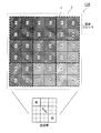
- FIG. 10 is a schematic diagram of an imaging region of the solid-state imaging device according to Embodiment 2 of the present invention.
- the solid-state imaging device 120 shown in the figure is described in Embodiment 1 only in that it has a light attenuation filter 16 for each pixel block composed of a plurality of unit pixels 1 in 2 rows and 2 columns.
- Different from the solid-state imaging devices 100 and 110 Hereinafter, description of the same points as the solid-state imaging devices 100 and 110 will be omitted, and only different points will be described.
- the plurality of unit pixels 1 in the imaging region 2 shown in FIG. 10 are arranged in a Bayer array.
- An independent light attenuation filter 16 is provided for each pixel block that is one unit of the Bayer array, and the light attenuation filter 16 is driven for each Bayer array.
- FIG. 10 shows a state in which the light attenuation filter 16 of the upper left pixel block is set to 100% transmittance, and the lower the pixel block at the lower right, the higher the attenuation factor is set.
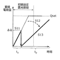
- FIG. 11A is an operation flowchart of the signal processing apparatus according to Embodiment 2 of the present invention.
- FIG. 11B is a graph showing the adjustment operation of the accumulated charge amount of the photoelectric conversion unit by the signal processing device.
- the exposure time is set so that the accumulated charge is not saturated and the gradation of the low-luminance subject can be expressed in the imaging exposure (step S13) shown in FIG. 11A. Is done.
- the signal processing apparatus includes a specifying unit that specifies a region that outputs a saturation signal from a luminance signal intensity distribution of an imaging region acquired in advance by preliminary imaging, and a region that outputs a saturation signal specified by the specifying unit.
- the light attenuating filter 16 is set by setting an applied voltage to the light attenuating filter 16 disposed in the pixel block before the image capturing exposure so that the luminance signal at the time of the image capturing exposure of the included pixel block is equal to or lower than the saturation signal.
- a transmittance control unit for electrically controlling the transmittance of the light.
- the specifying unit performs luminance signal saturation measurement in the exposure period t1 for each pixel block (step S11).
- the transmittance control unit determines that the output from the pixels in the same pixel block is (T / 100) ⁇ ( ⁇ Q / t1) ⁇ t2 ⁇ Q sat (Formula 1)
- T (%) is set for each pixel block so as to satisfy (Step S12).
- Q sat is the saturation charge amount.
- the signal processing apparatus performs imaging exposure on all the pixel blocks using the attenuation rate T set for each pixel block in step S12 (step S13).
- the light attenuation filter 16 is disposed for each pixel block, saturation determination is performed for each pixel block, and exposure conditions are set for each pixel block. A wide dynamic range that is not saturated with respect to a high-luminance pixel region can be realized.
- FIG. 12 is a schematic diagram of an imaging region of the solid-state imaging device according to Embodiment 3 of the present invention.
- the solid-state imaging device 130 shown in the figure has the light attenuation filter 16 only in the R1 pixel and the R2 pixel in the pixel block of the Bayer array composed of the plurality of unit pixels 1 in 2 rows and 2 columns. Only the points differ from the solid-state imaging device 120 described in the second embodiment. Hereinafter, description of the same points as the solid-state imaging device 120 is omitted, and only different points will be described.
- the light attenuation filter 16 is disposed only above the G1 and G2 pixels having the highest visibility in the pixel block that is one unit of the Bayer array.
- the determination unit included in the signal processing device determines in advance whether or not the luminance signals output from the G1 pixel and the G2 pixel are saturated before imaging exposure, and the transmittance control unit included in the signal processing device is determined by the determination unit.
- the applied voltage to the light attenuation filter 16 is set before the image capturing exposure so that the luminance signal at the time of image capturing exposure is equal to or lower than the saturation signal.
- the rate is electrically controlled.
- the light amount adjustment of the G pixel is effective for suppressing the saturation of the luminance signal. As a result, it is possible to realize a wide dynamic range without reducing the S / N of the B signal and R signal with a small signal amount. Further, since the electrochromic driving area is only the area of the green pixel, the driving power can be reduced, and thus a wide dynamic range can be realized with low power consumption.
- FIG. 13 is a structural sectional view of the optical attenuation filter 36 according to the fourth embodiment of the present invention and a diagram showing the driving principle.
- the light attenuation filter 36 described in FIG. 13 is described in FIG. 5 according to the first embodiment only in that the insulating layer 35 is inserted between the solid electrolyte layer 34 and the active material layer 33. Different from the optical attenuation filter 16.
- description of the same points as the light attenuation filter 16 will be omitted, and only different points will be described.
- the light attenuation filter 36 is an electrochromic element using a solid electrolyte, and thus basically requires a pair of transparent electrodes, a solid electrolyte as an insulator, and an active material in which an oxidation-reduction reaction is performed. It is. Moreover, since the electron movement of the active material layer 33 is accompanied by the ion movement, the solid electrolyte layer 34 must be an insulator. This is because the electronic structure of the active material layer 33 is changed due to the reduction reaction and becomes conductive. Therefore, if there is a leakage current on the solid electrolyte layer 34 side, it becomes a capacitor structure, but it becomes a simple resistance and redox. This is because no reaction can occur.
- transition metal oxides such as Ta 2 O 5 and V 2 O 5, which are typical constituent elements of the solid electrolyte layer 34, tend to cause oxygen vacancies as leak sources, and the larger the device area, the more these elements. Leakage causes power loss and makes it impossible to cause sufficient ion movement. In addition, there is a problem with reliability that defects increase due to Joule heat caused by leakage current and leakage increases. Therefore, in order to ensure the insulation of the capacitor structure, it is preferable to insert a thin film insulating layer that is insulative and allows only ions to pass between the solid electrolyte layer 34 and the active material layer 33.
- the insulating layer 35 As a material of the insulating layer 35 which is the thin film insulating layer, SiO 2 , SiON, or SiN is preferable.
- SiO 2 is used as the material of the insulating layer 35, for example, the film thickness is about 5 nm.
- the film forming method is preferably plasma CVD, but may be a reactive sputtering method or a PLD method.
- SiO 2 has excellent insulating properties and is suitable for ion migration of hydrogen, Li and the like.
- the thickness should be as thin as possible, and preferably about 1 to 10 nm.
- the above configuration of the light attenuation filter 36 makes it possible to maintain insulation even when a leak source is present in the solid electrolyte layer 34 made of a transition metal oxide. Therefore, the variation in the transmittance within the surface of the light attenuation filter 36 is suppressed, the reproducibility of the transmittance is ensured, and the transmittance can be maintained for a long time. Therefore, it is possible to provide a solid-state imaging device equipped with a high-performance optical attenuation filter with a high yield.
- Embodiment 5 a solid-state imaging device in which the material configuration of the solid electrolyte layer is different will be described.
- the solid-state imaging device according to the present embodiment is different from the solid-state imaging devices 100 and 110 according to the first embodiment only in the material configuration of the solid electrolyte layer included in the light attenuation filter.
- description of the same points as the light attenuation filter 16 will be omitted, and only different points will be described.
- the solid-state imaging device 140 includes a light attenuation filter 46.
- the light attenuation filter 46 includes a transparent electrode 31, a solid electrolyte layer 47, an active material layer 33, and a transparent electrode 32 in the order of lamination.
- the solid electrolyte layer 47 is made of one of oxides of zirconia, tantalum, chromium, vanadium, niobium, and hafnium containing any one of Li, Na, and Ag.
- An example of the material of the solid electrolyte layer 47 is LiV 2 O 5 .
- the ion conduction medium of the light attenuating filter 46 according to the present embodiment is hydrogen ions, it is not necessarily hydrogen from the viewpoint of device reliability.
- the principle of changing the transmittance of the active material layer 33 is that electrons are injected at the same time as ions are inserted into the active material layer 33 and a reduction reaction occurs in which the valence of the central metal ion is reduced.
- the ion to be inserted may be anything as long as it can move in the solid. However, since it is an element that diffuses in a solid and has excellent controllability, hydrogen having the smallest atomic radius and ion radius is most suitable. However, on the other hand, in device operation, hydrogen is not necessarily optimal due to the influence of the operating environment on the reliability and the process yield. For example, degassing due to high temperature operation may occur.
- Li + is used as ions.
- Li along with H, has a small ionic radius and a very small ionization potential, and thus easily causes a redox reaction.
- hydrogen annealing or acid immersion has been described as a method for introducing hydrogen.
- Li can be handled as a solid material source of the film forming apparatus, so that quantitative introduction of Li is possible.
- the amount of Li introduced may be an indefinite ratio as the chemical composition, but since it is used as a solid material source of the film forming apparatus, in this embodiment, what is expressed as LiV 2 O 5 as a chemical formula is used.
- Li is used as an ionic element.
- an alkali metal that easily causes redox may be used as long as the ionization potential is low.
- the ion radius must be small, and Li or Na is suitable.
- the valence is preferably 1, and for example, AgV 2 O 5 containing Ag may be used.
- zirconia, tantalum, chromium, vanadium, niobium or hafnium oxides are suitable as solid electrolyte materials that contain Li or Ag and can exist stably.
- metal ions as the ion conduction medium, it is possible to form a solid electrolyte whose composition is quantitatively controlled, and it is possible to manufacture a light attenuation filter having high uniformity. Therefore, the transmittance of the light attenuation filter can be controlled more accurately, and a solid-state imaging device with high yield and high reliability can be provided.
- the solid-state imaging device and imaging device of the present invention can provide a high-performance, high-performance camera having a wide dynamic range, a small size, and a light amount adjustment function. it can.
- the amount of light reaching the pixel block in the luminance saturation region can be attenuated by the light attenuation filter. Therefore, even if the saturation charge amount is reduced by pixel miniaturization, a wide dynamic range can be realized, and the light quantity can be adjusted under high illuminance without a mechanical diaphragm mechanism. Therefore, it is possible to provide a solid-state imaging device capable of obtaining a high-definition image having a small dynamic imaging range and a wide dynamic range.
- the solid-state imaging device and the imaging device of the present invention have been described based on the embodiments, the solid-state imaging device and the imaging device according to the present invention are not limited to the above-described embodiments.
- CMOS type solid-state imaging device has been described as an example.
- the present invention is not limited to this, and a CCD-type solid-state imaging device can achieve the same effect.
- the present invention is particularly useful for a digital camera, and is optimal for use in a solid-state imaging device and camera that require a wide dynamic range and high-quality images.
Landscapes
- Engineering & Computer Science (AREA)
- Multimedia (AREA)
- Signal Processing (AREA)
- Physics & Mathematics (AREA)
- Spectroscopy & Molecular Physics (AREA)
- Solid State Image Pick-Up Elements (AREA)
- Chemical & Material Sciences (AREA)
- Inorganic Chemistry (AREA)
- Transforming Light Signals Into Electric Signals (AREA)
- Blocking Light For Cameras (AREA)
Abstract
絞り機構がなくても光量を調整することが可能で、高照度下においても広いダイナミックレンジにて撮像することが可能な固体撮像装置を提供する。半導体基板(20)の表面に形成された光電変換部(11)を備える単位画素(1)が二次元状に複数個配列した撮像領域を有する固体撮像装置であって、光電変換部(11)の上に形成された、誘電体からなる層間膜(24)と、層間膜(24)の上に、画素部単位で、または、複数の画素部からなる画素ブロック単位で形成された、電圧印加により光の透過率が変化する光減衰フィルタ(16)と、半導体基板(20)内であって光減衰フィルタ(16)に対応して形成され、光減衰フィルタ(16)への電圧印加経路を確保または遮断する選択トランジスタとを備える。
Description
本発明は、デジタルスチルカメラなどに搭載される固体撮像装置及び撮像装置に関する。
デジタルスチルカメラによる撮像には、被写体や撮影場所の照度に合わせて光量を調節する外付けのND(Neutral Density)フィルタや機械式の機械式絞りが用いられているが、両者とも固体撮像装置とは別素子として動作させるため、カメラの小型化が困難である。よって、特に、セキュリティ用デジタルカメラや携帯電話端末用カメラなどの小型カメラ類には、上記外付けのNDフィルタや機械式の機械式絞りは用いられていない。
さらには、画像の高精細化と素子の小型化の要請から画素の微細化が進められており、フォトダイオードの縮小によって撮像飽和照度が低下し、晴天時の屋外など高照度下での撮像においてフォトダイオードが飽和してしまい、画像が白くつぶれてしまう、いわゆる白とびなどが課題となっている。特に飽和照度が減少することで、同一の画角の中で照度の高いところと低いところとが混在した場合に、両者の信号が飽和しないように明暗として撮像することが極めて困難になる。そのため、光量調節機構なしでの高照度下撮像が困難となっている。
特許文献1では、機械式絞りを使わないカメラとして、カメラ内部に収納された固体撮像素子と、当該固体撮像素子の撮像面と平行に配置されてパッケージに一体化され、通電することにより透過光を制御する光量調整手段とを備えた固体撮像装置が開示されている。
図14は、特許文献1に記載された従来の固体撮像装置の構造断面図である。同図に記載された固体撮像装置508には、CCD(Charge Coupled Device)素子501の撮像面をボンディング処理したCCDパッケージ502内部に、光量調整ユニット503が配置されている。光量調整ユニット503は、ガラス板504、透明導電膜505、エレクトロクロミック膜506及び電解膜507を枠503aでユニット化して形成された公知のエレクトロクロミック素子である。エレクトロクロミック膜506は、端子A及び端子Bからの電圧印加によりグレーに着色し、また逆極性の直流により無色に消色する現象を示す。この現象を利用することで、光量調整ユニット503の透過光強度が調整される。上述したように、固体撮像装置508は、光量調整手段としてエレクトロクロミック素子が用いられていることにより、電圧印加により光の透過率を可逆に変化させることができる。この構成によれば、高照度下においても光量が調節された撮像が可能となる。さらに、エレクトロクロミック素子により、モータなどの機械的機構が用いられず薄膜が用いられることから、カメラの小型化が実現できるとしている。
しかしながら、特許文献1に記載された固体撮像装置の構造では、画角内の光量を均一に減少させる効果のみとなっているため、同一画角内におけるダイナミックレンジを低下させてしまうという課題を有する。例えば、画角内に高輝度の被写体と低輝度の被写体が存在した場合、図14に記載されたエレクトロクロミック素子を用いたフィルタによって光透過量を制限することで、低輝度の被写体の信号強度が減少し、S/Nの悪化が避けられない。
また、特許文献1に記載された固体撮像装置の構造では、光量調整ユニット503を封止するためのガラス板504は、CCD素子501とは個別に光軸上に設けられている。そのため、CCD素子501の表面と光量調整ユニット503との間での多重反射に起因したゴーストやフレアと呼ばれる擬似像や擬似信号が発生し、画質を劣化させてしまうという課題を有する。
上述のように、ゴーストやフレアを抑制するとともに、高照度下でも撮像できる広ダイナミックレンジを有する固体撮像装置が求められている。
本発明は、上記課題に鑑みてなされたものであり、絞り機構がなくても光量を調整することが可能で、高照度下においても広いダイナミックレンジにて撮像することが可能な固体撮像装置を提供することを目的とする。
上記の課題を解決するために、本発明の一態様に係る固体撮像装置は、半導体基板表面に形成された光電変換素子を備える画素部が二次元状に配列された撮像領域を有する固体撮像装置であって、前記光電変換素子の上に形成された、誘電体からなる層間膜と、前記層間膜の上に、画素部ごとに、または、複数の画素部からなる画素ブロックごとに対応して形成された、電圧印加により光の透過率が変化する光減衰フィルタと、前記半導体基板内に前記光減衰フィルタに対応して形成され、前記光減衰フィルタへの電圧印加経路を接続または遮断するためのスイッチングトランジスタとを備えることを特徴とする。
本態様によれば、画素部または画素ブロックごとに、透過率の調整が可能な光減衰フィルタが配置されているので、画素部または画素ブロックごとの露光条件の設定が可能となる。よって、画角内に高輝度被写体と低輝度被写体が混在した場合でも、画素部または画素ブロックごとに光透過量を制限できるので、低輝度被写体の明暗を鮮明に表現すると同時に、高輝度の画素領域に対して飽和しない広いダイナミックレンジを実現することができる。
また、光減衰フィルタは、誘電体からなる層間膜を介して光電変換部上に、画素部または画素ブロック単位で積層形成されているので、多重反射に起因したゴーストやフレアを抑制することが可能となる。
また、前記光減衰フィルタは、前記誘電体からなる層間膜上に積層された下部透明電極と、前記下部透明電極上に積層された固体電解質層及び活物質層と、前記固体電解質層及び前記活物質層のうちの上層の上に積層された上部透明電極とを備え、前記固体電解質層は、絶縁性の誘電体からなり、前記下部透明電極及び前記上部透明電極への電圧印加によりイオンの挿入及び放出を発生させる材料であり、前記活物質層は、電圧印加による前記イオンの挿入及び放出に伴い光の吸収スペクトルが変化する材料であることが好ましい。
これにより、光減衰フィルタの薄膜化が実現できることから、高精細な画像を得ることができる小型の固体撮像装置を実現することが可能となる。
また、前記活物質層は、WO3、MoO3またはIrO2からなるアモルファスの膜であることが好ましい。
これにより、薄膜で透明と深青での色変換が可能であることから、広ダイナミックレンジを実現できる小型の固体撮像装置を実現することが可能となる。
また、前記固体電解質層は、ZrO2、Ta2O5、Cr2O3、V2O5、SiO2、Nb2O5及びHfO2のうちの少なくとも1つからなり、水素を含有していてもよい。
これにより、水素をイオン伝導の媒体とすることから固体電解質中へのイオンの導入が容易であり、水素のイオン半径が小さいことから光減衰フィルタの高速な切り替えが可能となる。よって、製造コストが低く高速動作が可能な固体撮像装置を提供することができる。
また、前記固体電解質層は、Li、Na及びAgのうちの少なくとも1つを含むジルコニア、タンタル、クロム、バナジウム、ニオブ及びハフニウムの酸化物のうちの1つによって構成されていてもよい。
これにより、不揮発性元素のLi、NaまたはAgをイオン伝導媒体として用いることから、固体電解質へのイオン導入を定量的に行えるため、光減衰フィルタの透過率のばらつきを低減するとともに、透過率をより正確に制御できる。よって、高歩留まり、高精細及び広ダイナミックレンジを有する固体撮像装置を提供することが可能となる。
また、前記光減衰フィルタは、さらに、前記固体電解質層と前記活物質層との間に、絶縁体からなる薄膜絶縁層を備え、前記絶縁体は、SiO2、SiON及びSiNのいずれか1つであってもよい。
これにより、薄膜絶縁層を、固体電解質層と活物質層との間に挿入することで、エレクトロクロミック素子のリーク電流を抑えることが可能となる。よって、光減衰フィルタの面内の透過率のばらつき抑制、透過率の再現性確保、及び透過率の長時間維持が図られる。よって、高歩留まりで高性能な光減衰フィルタを搭載した固体撮像装置を提供することが可能となる。
また、前記固体撮像装置は、N2または希ガスによって満たされた、気密封止されたパッケージ内に設置されていることが好ましい。
これにより、酸素や水がパッケージ内にないことから、固体電解質及び透明電極の酸化や還元が進行しない。よって、安定した動作と高い信頼性を実現できる固体撮像装置を提供することが可能となる。
また、上記の課題を解決するために、本発明の一態様に係る撮像装置は、上述した固体撮像装置の態様のうちいずれか一態様に係る固体撮像装置と、前記撮像領域に入射する光量を調節するための信号処理装置とを備え、前記信号処理装置は、前記画素部から出力される輝度信号が飽和するかどうかを、撮像露光の前に予め判定する判定部と、前記判定部により前記輝度信号が飽和すると判定された場合、前記撮像露光時の輝度信号が飽和信号以下となるように、前記撮像露光の前に、前記光減衰フィルタへの印加電圧を設定することにより前記光減衰フィルタの透過率を電気的に制御する透過率制御部とを備えることを特徴とする。
本態様によれば、予め実行される輝度信号飽和判定によって、撮像露光時の光透過量を光減衰フィルタで制御することから、小型化が実現でき、高照度下においても撮像が可能となる撮像装置を提供することができる。
また、本発明の一態様に係る撮像装置は、前記固体撮像装置が、2行2列の画素部で構成される画素ブロック毎に前記光減衰フィルタを備え、前記信号処理装置は、さらに、予め取得した前記撮像領域の輝度信号強度分布から飽和信号を出す領域を特定する特定部を備え、前記透過率制御部は、前記特定部により特定された前記領域に含まれる画素ブロックの前記撮像露光時の輝度信号が飽和信号以下となるように、前記撮像露光の前に、前記画素ブロックに配置されている前記光減衰フィルタへの印加電圧を設定することにより前記光減衰フィルタの透過率を電気的に制御してもよい。
これにより、画素ブロックごとに飽和判定をすることから、飽和信号が得られる画素ブロックごとに光の透過率を制御でき、高輝度と低輝度の被写体を同時に撮像できる広いダイナミックレンジを実現する固体撮像装置を提供することが可能となる。
また、本発明の一態様に係る撮像装置は、前記固体撮像装置が、2行2列の画素部で構成される画素ブロックを有し、前記画素ブロックは、緑色の信号を得るG1画素部及びG2画素部と、赤色の信号を得るR画素部と、青色の信号を得るB画素部からなるベイヤー配列を構成しており、前記光減衰フィルタは、前記G1画素部とG2画素部の上部にのみ配置されており、前記判定部は、前記G1画素部及びG2画素部から出力される輝度信号が飽和するかどうかを、撮像露光の前に予め判定し、前記透過率制御部は、前記判定部により前記輝度信号が飽和すると判定された場合、前記撮像露光時の輝度信号が飽和信号以下となるように、前記撮像露光の前に、前記光減衰フィルタへの印加電圧を設定することにより前記光減衰フィルタの透過率を電気的に制御してもよい。
これにより、視感度の最も高い緑色信号のみに光減衰フィルタを設けることで、光減衰フィルタの駆動面積が小さくなり、駆動電力が低減できるとともに、視感度の低い赤や青の感度を維持しながら、高輝度撮像が可能となることから、低消費電力で広いダイナミックレンジを実現する固体撮像装置を提供することが可能となる。
本発明の固体撮像装置によれば、画素部または画素ブロック毎にエレクトロクロミック素子からなる光減衰フィルタを形成することによって、薄膜化と小型化が可能となる。また、本発明の撮像装置によれば、飽和信号判定により光減衰フィルタの透過率調整を行う信号処理装置を設けることで、撮像領域内における輝度に合わせて光の透過率を制御することが可能となる。よって、広いダイナミックレンジを実現でき、高照度下でも撮像が可能となる固体撮像装置を提供することができる。
以下、本発明の実施の形態について図面を参照しながら説明する。
(実施の形態1)
図1は、本発明の実施の形態1に係る撮像装置の構成を示す機能ブロック図である。同図に記載された撮像装置200は、固体撮像装置100と、レンズ201と、駆動回路202と、信号処理装置203と、外部インターフェイス部204とを備えるデジタルカメラである。
図1は、本発明の実施の形態1に係る撮像装置の構成を示す機能ブロック図である。同図に記載された撮像装置200は、固体撮像装置100と、レンズ201と、駆動回路202と、信号処理装置203と、外部インターフェイス部204とを備えるデジタルカメラである。
信号処理装置203は、駆動回路202を通して固体撮像装置100を駆動し、固体撮像装置100からの出力信号を取り込み、内部処理した信号を、外部インターフェイス部204を介して外部に出力する。
固体撮像装置100は、入射光量を減衰させるための能動的な光減衰フィルタを画素部単位または画素ブロック単位で有し、信号処理装置203は、光減衰フィルタの減衰率を予め画素部単位または画素ブロック単位で設定することにより、撮像領域に入射する光量を調節することが可能である。
この構成によれば、被写体の輝度に合わせて撮像領域に到達する光の透過量を制御することがきることから、高照度下での撮像が可能となる。また、上記機能を、例えば、ベイヤー配列毎に設置することで低輝度被写体と高輝度被写体とを同時に諧調表現することが可能となる。以下、本発明の要部である固体撮像装置100及び信号処理装置203について詳細に説明する。
図2は、本発明の実施の形態1に係る固体撮像装置の有する画素ブロックの回路構成図である。同図に記載された固体撮像装置100は、フォトダイオードである光電変換部11を有する単位画素1が二次元状に配列された撮像領域2と、画素信号を選択するための水平シフトレジスタ3及び垂直シフトレジスタ4と、選択された単位画素1からの信号を外部に与える出力端子5とを備える。
撮像領域2は、複数の単位画素1を含む。単位画素1は、光電変換部11と、転送用トランジスタ12と、リセット用トランジスタ13と、増幅用トランジスタ14と、選択トランジスタ15とを備える。転送用トランジスタ12、リセット用トランジスタ13、増幅用トランジスタ14及び選択トランジスタ15は、それぞれ、MOSトランジスタで構成されている。
さらに、固体撮像装置100は、光減衰フィルタ16と、選択トランジスタ17とを備える。光減衰フィルタ16は、撮像領域2の入射光側に形成されている。また、選択トランジスタ17は、電圧線18と光減衰フィルタ16との間に配置されている。選択トランジスタ17のゲートは、読み出し線19に接続されており、読み出し線19からの制御信号により、電圧線18と光減衰フィルタ16との導通及び非導通を切り替える。
電圧線18には、正電位と負電位の両方を選択的に印加することが可能となっている。この構成により、光減衰フィルタ16の透過率を減少させる場合には、例えば、電圧線18に正電圧を印加し、選択トランジスタ17を導通状態にすることで、光減衰フィルタ16に正電圧を印加する。また、選択トランジスタ17の導通期間、つまり、光減衰フィルタ16への正電圧の印加期間を制御することにより、光減衰フィルタ16の所望の透過率を得ることが可能となる。その後、選択トランジスタ17を非導通状態にし、設定した透過率の状態で通常の撮像駆動を行う。上記撮像駆動の終了後には、電圧線18に負電圧を印加し、選択トランジスタ17を導通状態にして光減衰フィルタ16を元の状態に戻す。
光減衰フィルタ16の透過率調整動作及び光電変換部11のリセット動作は、単位画素1の撮像動作とは時系列として順番に行うため、後述する輝度信号飽和測定及び撮像動作の前に光電変換部11に蓄積された電荷をリセットすることが可能である。上記構成により、新たな信号線を設置することなく、光減衰フィルタ16の透過率調整動作、単位画素1の撮像動作及びリセット動作は、個別に動作させることが可能となる。
なお、本実施の形態では、光減衰フィルタ16への電圧印加を制御するための選択トランジスタ17を設けたが、電圧線18をパルス駆動にすることで選択トランジスタ17を不要にすることも可能である。光減衰フィルタ16の透過率調整動作のときは、読み出し線19をOFFにしておけばよく、また、露光期間には電圧線18を0Vにしておけば、透過率調整動作により設定された透過率が露光中に変化することない。また、光電変換部11からの信号読み出し時には、電圧線18に電圧が印加されるが、その際に光減衰フィルタ16の透過率が変化しても、既に電荷蓄積後であれば擬似信号になることはなく、読み出し後に再び読み出し線19をOFFにして光減衰フィルタ16をOFFにすればよい。この構成にすることで、光減衰フィルタ16への電圧印加を制御するためのトランジスタが必要なくなるため、微細画素に対しても画素ごとへの光減衰フィルタ16の搭載が可能となる。
(透過率調整原理)
次に、本発明の実施の形態1に係る信号処理装置203について説明する。本発明のような能動的な光減衰フィルタ16を駆動させるためには、光をどの程度減衰させる必要があるかを予め判定しておく必要がある。そこで、本発明では、被写体を撮像する直前に、信号処理装置203によって輝度信号飽和判定を行うための予備撮像を導入している。
次に、本発明の実施の形態1に係る信号処理装置203について説明する。本発明のような能動的な光減衰フィルタ16を駆動させるためには、光をどの程度減衰させる必要があるかを予め判定しておく必要がある。そこで、本発明では、被写体を撮像する直前に、信号処理装置203によって輝度信号飽和判定を行うための予備撮像を導入している。
信号処理装置203は、単位画素1または複数の単位画素1からなる画素ブロックから出力される輝度信号が飽和するかどうかを、撮像露光の前に予め判定する判定部と、当該判定部により輝度信号が飽和すると判定された場合、撮像露光時の輝度信号が飽和信号以下となるように、撮像露光の前に、光減衰フィルタ16への印加電圧を設定することにより光減衰フィルタ16の透過率を電気的に制御する透過率制御部とを備える。
図3Aは、本発明の実施の形態1に係る信号処理装置の動作フローチャートである。また、図3Bは、光電変換部の蓄積電荷量と蓄積時間との関係を表すグラフである。
本実施の形態では、まず、信号処理装置203により輝度信号飽和測定を行い(ステップS01)、光減衰フィルタ16の透過率を減少させてから(ステップS02)、被写体の撮像を行う(ステップS03)というものである。
信号処理装置203の判定部は、まず、輝度信号飽和測定として、期間t1の露光により蓄積された蓄積電荷量ΔQから、図3Bに示すグラフの傾きに相当するΔQ/t1を算出する。そして、光減衰フィルタ16で入射光を減衰させなかった場合に必要とされる露光期間における輝度信号が飽和するか、つまり当該期間における蓄積電荷量が飽和電荷量に到達するかを信号処理領域で判定する。
信号処理装置203は、信号処理領域に、予め輝度信号強度に対する閾値を設定しておく。そして、透過率制御部は、輝度信号が上記閾値を超える場合は、光減衰フィルタ16を動作させ、蓄積効率に相当するΔQ/t1を透過率Tだけ減少させて飽和を防ぐようにする。
上記構成により、高照度下における撮影や高輝度被写体に対して、光電変換部11が飽和照度や飽和輝度にあるかどうかを判定し、光電変換部11が飽和しないように光減衰フィルタ16の光透過率を制御できる。よって、高照度下での撮像が可能となる。
本態様によれば、予備撮像により予め実行される輝度信号飽和判定によって、撮像露光時の光透過量を光減衰フィルタ16で制御することから、小型化が実現でき、高照度下においても撮像が可能となる撮像装置200を提供することが可能となる。
次に、光減衰フィルタの構造と動作原理ついて説明する。
図4は、本発明の実施の形態1に係る固体撮像装置の有する単位画素の断面概略図の一例である。同図に記載された単位画素1は、光電変換部11と、光減衰フィルタ16と、半導体基板20と、ゲート及びゲート配線22と、層間膜24と、カラーフィルタ26と、平坦化膜27と、マイクロレンズ28と、配線層57及び59とを含む。
光減衰フィルタ16は、最上の配線層59の上部であってカラーフィルタ26の下部に配置されている。配線層57及び59の配線材料は、例えば、AlCuである。また配線層数は、配線層57及び59の2層である。
また、光減衰フィルタ16は、透明電極31及び32と、活物質層33と、固体電解質層34とを備え、活物質層33と固体電解質層34との積層膜を透明電極31及び32で挟んだキャパシタ構造を有している。透明電極31及び32は、それぞれ、配線層59と電気的に接続されており、配線層59を介して半導体基板上に形成された選択トランジスタ17(図示せず)と電気接続された下部透明電極及び上部透明電極である。前述したように、光減衰フィルタ16は、選択トランジスタ17の導通及び非導通により印加電圧が制御される。
次に、光減衰フィルタ16の原理について説明する。
図5は、本発明の実施の形態1に係る光減衰フィルタの構造断面図及び駆動原理を表す図である。本実施の形態における光減衰フィルタ16は、エレクトロクロミック素子を用いている。
エレクトロクロミック素子とは、電圧印加によって材料の吸収スペクトルが変化し、色が変化する素子の総称である。例えば、液晶のように、電界により液晶分子の配向が変化することで透過率が変化する素子もエレクトロクロミック素子の一つである。中でも、固体中のイオン移動によって引き起こされる酸化還元反応によって吸収スペクトルを変化させる固体電解質を用いたエレクトロクロミック素子は、液晶のような偏光依存性もなく、また、特異なスペクトルを示す材料も存在することから、表示素子などに広く使われている。
図5の(a)に示された状態Aは、正の電圧が活物質層33側の透明電極32に印加されることで、活物質層33の活物質が酸化状態となっていることを示している。これにより、活物質層33から固体電解質層34へイオンが移動すると同時に、活物質層33から透明電極32へ電子が放出される。この状態Aでは、光減衰フィルタ16は透明状態となる。
一方、図5の(b)に示された状態Bは、負の電圧が活物質層33側の透明電極32に印加されることで、固体電解質層34中の陽イオンが活物質層33側に挿入されると同時に、透明電極32から活物質層33へ電子の注入が起こる還元状態を示している。
状態Aと状態Bとでは電圧の極性が反転しているだけであり、印加電圧として負側のみ、正側のみ、及び正負の両方、のうちいずれを用いてもかまわない。ただし、伝導イオンは基本的に陽イオンであるため、電子の方向とは逆向きに陽イオンが動くことになる。このエレクトロクロミックにおいては、活物質からイオンの移動量に対応した酸化還元電流に相当する電流が出入りする。このため、電極への電圧印加時間によってイオンの移動量を制御することができ、これにより光の透過量を制御することが可能となり、高照度下でも撮像が可能な固体撮像装置を実現できる。
次に、光減衰フィルタ16の構成材料について説明する。光減衰フィルタ16を構成する活物質層33は、アモルファスのWO3、MoO3、IrO2で表記される酸化物のうち、いずれか一つの材料から成る。また、固体電解質層34は、少なくともZrO2、Ta2O5、Cr2O3、V2O5、SiO2、Nb2O5、HfO2で示される酸化物材料の一つから成る。
一例として、活物質層33の構成材料としてWO3を、また、固体電解質層34の構成材料としてTa2O5を用いた場合を説明する。WO3とTa2O5との組み合わせはエレクトロクロミック素子では一般的な組み合わせの一つである。透明電極31及び32への電圧印加に応じて、WO3とTa2O5との間でイオン移動を伴う酸化還元反応が生じWO3の電子構造が大きく変化することにより、光減衰フィルタ16の透明状態と着色状態との間を段階的に制御することができる。
ここで、活物質層33の着色の原理を、WO3を例にして説明する。WO3はイオン性の高い酸化物であり、WO3のWは価電子をOに奪われたW6+に近い状態で存在する。この状態では約3.8eV程度のバンドギャップが存在する透明材料であるが、ここに水素やアルカリ金属などが存在すると、それらがWとOとの間に入り込み、自身の電子をW側に与える還元反応を引き起こす。この還元電子がWのd電子準位を占有し、光吸収に大きく寄与する。
図6は、水素導入前後におけるWO3の光透過スペクトルを表す図である。HxWO3は不定比で水素がWO3に導入された状態である。同図に示されるように、水素がない状態(WO3)では、可視光領域は透明度が非常に高いことがわかる。一方、水素を導入したHxWO3では、緑から赤にかけて強い光吸収が観測される。比較的光吸収が小さい青色領域においても、透過率が40%程度も低下しており、もともと青色は視感度も低い色であることから、十分な可視光線の光減衰フィルタとなる。
また、活物質層33は、アモルファス膜の方が望ましい。WO3が結晶の場合、水素などのイオンが入るサイトが少なくなると同時に、イオン移動速度が遅くなってしまう。しかし、アモルファス状態では、イオンが入るサイト数が多く、イオン伝導速度も結晶状態に比べて速いため、アモルファス膜が本発明には最適といえる。さらに、アモルファスWO3は低温で成膜が可能であることから、シリコンプロセスとの親和性も非常に高い。
また、Wと同属のMoの酸化物であるMoO3及びイオン性が強いIrの酸化物であるIrO2においても同様の動作原理によって透明状態と着色状態との間でエレクトロクロミック現象が生じる。つまり、イオン移動によって光透過率が変化する透明酸化物材料であって、WO3、MoO3、IrO2は応答性や製造の簡便性などから優れている。
次に、固体電解質層34について説明する。本実施の形態ではH+イオンを伝導イオンとして用いており、活物質層33との間でH+イオンを出し入れするため、H+イオンの貯蔵とH+イオンの移動が容易である透明材料が求められる。また、伝導イオンは固体電解質層34及び活物質層33内の電界によって駆動されるため、固体電解質層34には絶縁性が求められる。ZrO2、Ta2O5、Cr2O3、V2O5、SiO2、Nb2O5及びHfO2は、絶縁性に優れた透明酸化物誘電体であり、H+イオンを含有するとともに活物質へのイオンの供給が可能な材料である。H+イオンはイオン半径が最も小さいイオンであるため、イオンの拡散速度が速く光減衰フィルタ16の高速な切り替え動作が可能となる。このようにH+イオンの伝導においては本実施の形態が最良の形態である。
(製造方法)
ここで、本実施の形態に係るWO3およびTa2O5を用いた光減衰フィルタ16を搭載した固体撮像装置の製造方法の一例を説明する。
ここで、本実施の形態に係るWO3およびTa2O5を用いた光減衰フィルタ16を搭載した固体撮像装置の製造方法の一例を説明する。
エレクトロクロミック素子において、本発明の実施の形態1に係るデバイス構造は、一組の活物質層33及び固体電解質層34から成るエレクトロクロミック素子を最上の配線層59の上部に層間膜を隔てて設けられた構造であり、カラーフィルタ形成前に光減衰フィルタの形成プロセスが必要となる。以下、最上の配線層以降の製造プロセスについて詳細について説明する。
図7は、本発明の実施の形態1に係る変形例を示す固体撮像装置の構造断面図の一例である。同図に記載された固体撮像装置110は、MOS型イメージセンサである。また、図8は、本発明の実施の形態1に係る固体撮像装置の有する光減衰フィルタの工程断面図である。
図7に示されたように、半導体基板20に、イオン注入によって拡散領域52が形成されている。また、半導体基板20上には、画素部の撮像領域51及び周辺回路領域50が形成されている。
トランジスタ54は素子分離部53によって電気的に分離されている。トランジスタ54の形成後、BPSG(Boron Phosphor Silicate Glass)などの絶縁体からなる層間膜56を成膜し、CMP(Chemical Mechanical Polishing)やエッチバックによって平坦化した後、ドライエッチングによってコンタクトホールを形成し、メタルCVD法によって金属プラグ55を形成する。金属プラグ55が露出した状態でアルミをスパッタなどで成膜し、ドライエッチングでパターニングすることで配線層57を作製する。このプロセス構成を繰り返すことで多層配線構造を作ることができる。トランジスタ54は、例えば、図2に記載された転送用トランジスタ12、リセット用トランジスタ13、増幅用トランジスタ14、選択トランジスタ15及び17のいずれかに相当する。
本実施の形態に係る固体撮像装置110は、2層配線構造であるため、1層目の配線層57の上部に絶縁性の誘電体からなる層間膜24を形成して平坦化し、金属プラグを形成後、2層目の配線層59を形成する。
次に、光減衰フィルタ16の形成工程に移る。図8の(a)に示すように、絶縁性の誘電体からなる層間膜61をBPSGで形成し、CMPを用いて平坦化する。
次に、図8の(b)に示すように、金属プラグ60を形成する。ここで、金属プラグ60が露出した状態にする。
次に、図8の(c)に示すように、光減衰フィルタ16の透明電極31、固体電解質層34、活物質層33を積層成膜する。このとき、下部の透明電極31は、金属プラグ60に電気的に接続される。光減衰フィルタ16は、基本的に光を透過させる必要があるため、透明電極31は、可視光に対して透明なITOを用いる。透明電極31の膜厚は、例えば、200nmである。なお、本実施の形態では、2層の配線層57及び59の上部に光減衰フィルタ16を設けたが、画素構造においては特にこれに限る必要は無く、光減衰フィルタ16は、1層目の配線層57と2層目の配線層59との層間に設けてもよい。
次に、図8の(d)に示すように、ドライエッチングにより、素子分離のためのパターニングを行う。
次に、図8の(e)に示すように、BSPGやFSGのような絶縁性の層間膜67を堆積させ、CMPによる平坦化を行う。その後、酸化膜ドライエッチングにより、金属プラグ用ビアホールを形成する。その後、メタルCVDにより、金属プラグ65を含む金属を成膜する。
次に、図8の(f)に示すように、CMPにより、活物質層33のWO3が露出するまで表面を研磨する。
次に、図8の(g)に示すように、透明電極32を形成し、パターニングを行う。このとき金属プラグ65と透明電極32とが電気的に接続されるようにする。光減衰フィルタ16は、基本的に光を透過させる必要があるため、透明電極32は、可視光に対して透明なITOを用いる。
最後に、図8の(h)に示すように、平坦化膜70を形成する。その後、図示していないが、カラーフィルタ及びマイクロレンズを形成する。以上により、本発明の固体撮像装置110が形成される。
上記構成によれば、単位画素1の積層形成工程と連続して画素単位で透過率の調整が可能な光減衰フィルタ16が配置されているので、単位画素1または複数の単位画素1からなる画素ブロックごとの露光条件の設定が可能となる。よって、画角内に高輝度被写体と低輝度被写体が混在した場合でも、画素部または画素ブロックごとに光透過量を制限できるので、低輝度被写体の明暗を鮮明に表現すると同時に、高輝度の画素領域に対して飽和しない広いダイナミックレンジを実現することができる。
また、光減衰フィルタ16は、誘電体からなる層間膜24及び61を介して光電変換部上に画素と一体形成されるので、光減衰フィルタを画素とは個別に形成した後に画素上に配置した構造と比較して、多重反射に起因したゴーストやフレアを抑制することが可能となる。
ここで、透明電極31及び32、ならびに、固体電解質層34及び活物質層33の成膜方法について、詳細に説明する。
透明電極31及び32であるITO電極は、例えば、パルスレーザ成膜法(PLD法)を用いて作製する。PLD法とは、パルスレーザを所望の材料に集光照射し、材料表面が瞬間的、局所的に高温化することで材料原子が蒸発し、別の場所においた基板上に再付着させて成膜する方法である。レーザにより原子蒸発するターゲットとして酸化物を使用し、成膜雰囲気を酸素にすることで、均一性の高い酸化物成膜が可能となる。具体的には、例えば、ITOターゲットにエキシマレーザであるKrFレーザ(波長248nm)を照射し、配線上に成膜する。このとき、成膜温度は、アルミからなる配線層57及び59が溶解しない温度として300℃程度が好ましい。
なお、本実施の形態ではPLD法を紹介したが、反応性スパッタ成膜法や加熱蒸着法を用いてもよい。透明電極31及び32の膜厚は、薄すぎると抵抗が増加してしまうため、50nm以上が望ましい。一方、膜厚が厚すぎると、マイクロレンズから光電変換部11までの距離がマイクロレンズの焦点距離よりも長くなってしまい集光度を下げてしまう。本実施の形態では、ITOの膜厚は200nmとしたが、膜厚はできるだけ薄いほうが望ましい。
透明電極31の上部に、固体電解質層34と活物質層33とを積層する。本実施の形態では活物質層33及び固体電解質層34は、それぞれ、WO3及びTa2O5を用いており、それぞれの膜厚は、300nm及び200nmである。
本実施の形態においては、WO3膜及びTa2O5膜についてもPLD法を用いて成膜している。
ITOからなる透明電極31上に、酸素雰囲気中、成膜温度400℃程度で、Ta2O5を成膜する。上述したように、400℃程度よりも高温で成膜すると、アルミの配線層が溶解する恐れがあるためである。しかし、低温での酸化物成膜は酸化が十分に進行せず、酸素の供給不足によって低密度で酸素欠損が大量に含まれてしまい、絶縁性の低下や透過率の低下の原因となる。よって、この観点からはできる限り高温での成膜が望ましく、400℃程度での成膜としている。
Ta2O5成膜後には、400℃程度の水素アニールを1分間程度行うことでTa2O5中への水素導入を行う。長時間の水素アニールはTa2O5を還元してしまい、リーク電流の増加や透明性の減少に繋がるだけでなく、ITO透明電極の導電率の低下の原因ともなる。よって、過剰な水素が導入されないように最表面のTa2O5膜に低濃度の水素ドーピングするためには、水素アニールの時間と流量を制御する必要がある。なお、水素アニールの場合、WO3が水素原子を取り込むのに400℃程度の温度を必要としているが、希塩酸に10秒から60秒程度浸すことで水素を導入することも可能である。以上のようにして、固体電解質層34が形成される。
次に、再びPLD法により成膜温度200℃で、Ta2O5上に、WO3を成膜する。水素導入を施したTa2O5から水素の脱離を防ぐため、WO3の成膜は300℃程度よりも低い温度が望ましく、本実施の形態では200℃程度でWO3を成膜している。また、前述したように、本発明に係る活物質層33は、アモルファス膜の方が望ましい。WO3は結晶の場合、水素などのイオンが入るサイトが少なくなると同時に、イオン移動速度が遅くなってしまう。しかし、アモルファスはイオンが入るサイト数が多く、イオン伝導速度も結晶に比べて速いため、本発明には最適といえる。さらに、アモルファスWO3は低温で成膜が可能であることから、シリコンプロセスとの親和性も非常に高い。以上のようにして、活物質層33が形成される。
上述した光減衰フィルタ16の構成により、光減衰フィルタの薄膜化が実現できることから、高精細な画像を得ることができる小型の固体撮像装置を実現することが可能となる。
また、本実施の形態では、活物質層33と固体電解質層34に、それぞれ、WO3とTa2O5を用いたが、これに限るものではなく、イオン移動によって透過スペクトルが変化する材料であればよく、活物質層33としてはMoO3やIrO2などでも良い。これにより、薄膜で透明と深青での色変換をすることが可能となることから、広ダイナミックレンジを実現できる小型の固体撮像装置を実現することが可能となる。
また固体電解質層34においても、水素を含有しイオン伝導が可能な透明絶縁体であれば良く、ZrO2、Ta2O5、Cr2O3、V2O5、SiO2、Nb2O5、HfO2などでも良い。特にZrO2、Cr2O3及びV2O5などはイオン伝導性も優れているため有効な材料である。これにより、水素をイオン伝導の媒体とすることから固体電解質中へのイオンの導入が容易であり、水素のイオン半径が小さいことから光減衰フィルタ16の高速な透過率切り替えが可能となる。よって、製造コストが低く高速動作が可能な固体撮像装置を提供することができる。
なお、本実施の形態では固体電解質層34の上に活物質層33を積層させたが、活物質層33の上部に固体電解質層34を積層する構造でもかまわない。また、本実施の形態では、活物質層33の膜厚として200nm程度、固体電解質層34の膜厚として300nm程度としたが、それぞれの膜厚は、光の透過率、駆動速度、再現性の観点から非常に重要なパラメータである。膜厚が薄すぎると着色しても光が透過してしまい、光を十分に減衰させることができない。
一方、膜厚が厚すぎるとデバイスの層構造全体の膜厚が厚くなるため、マイクロレンズの焦点距離よりも全体の膜厚が大きくなり、光電変換部11への集光が低下してしまう。さらに、水素などのイオンが活物質の奥深くに侵入するため、逆電圧により全イオンを放出させ、活物質を透明化するために長時間を要することとなる。これは動作速度の低減を意味する。しかも、繰り返しの動作によって活物質層33側に徐々に水素が残留し、透過率変調の再現性が徐々に失われてしまう。よって、高濃度水素(などの伝導イオン)を活物質層33と固体電解質層34との界面近傍で効率よくやり取りすることが動作速度、再現性、透過率の変調に対して重要となる。
本実施の形態では、活物質層33及び固体電解質層34の双方をアモルファス材料とすることで伝導イオンが位置するサイト数が増え、高濃度の伝導イオンを含有することが可能となる。また、活物質層33の膜厚を、200nm程度とすることで、繰り返し動作の再現性を確保している。なお、100nm程度より薄い膜厚にすると着色時においても透過率が80%以上になり、光減衰フィルタとしての機能を果たすには不十分である。また、1000nm程度より厚い膜厚とすると、活物質層33から固体電解質層34へのイオン伝導の際に、活物質層33側に水素が残留し透明性を確保することが困難である。よって、活物質層33の膜厚は、100nm以上で1000nm以下が望ましい。
また、固体電解質層34の膜厚においても、活物質層33に挿入する十分な水素を含有でき、かつ活物質層33から効率よく水素を取り込むことができる体積が必要となるため、固体電解質層34の膜厚は活物質層よりも厚い方が望ましい。
(固体撮像装置の実装)
図9は、本発明の実施の形態1に係る固体撮像装置の実装状態を表す断面概略図である。
図9は、本発明の実施の形態1に係る固体撮像装置の実装状態を表す断面概略図である。
以下、固体撮像装置の実装工程を、図9を参照しながら説明する。
まず、接続ピン84を有するセラミックの台座80に、本発明の固体撮像装置100を接合する。次に、金属ワイヤ81を接続する。その後、気体82を封入して透明ガラス板83で封止する。
ここで、気体82は希ガスまたはN2を用いる。希ガスを用いる場合はArが最も低コストで適している。固体撮像装置100に含まれる固体電解質層34、活物質層33、透明電極31及び32はすべて酸化物から構成されており、過剰な水素は還元反応を引き起こすためできる限り水素の供給源を遠ざける方が信頼性の観点から望ましい。デバイス構造としては保護膜を施しているものの、雰囲気中に含まれる水分などから供給される水素原子が徐々に酸化物を還元し、エレクトロクロミック素子の特性を低下させる。そこで、Arなどの希ガスやN2ガスのような不活性ガスで封止することによって水素の供給源を絶ち、安定したデバイス動作を実現することができるとともに、高い信頼性を確保することが可能となる。
なお、図1に記載された撮像装置200が備える固体撮像装置100は、上述した実装状態で撮像装置200に組み込まれていることが好ましい。
(実施の形態2)
本実施の形態では、単位画素1がベイヤー配列している場合の固体撮像装置について説明する。
本実施の形態では、単位画素1がベイヤー配列している場合の固体撮像装置について説明する。
図10は、本発明の実施の形態2に係る固体撮像装置の撮像領域の模式図である。同図に記載された固体撮像装置120は、2行2列の複数の単位画素1で構成される画素ブロック毎に光減衰フィルタ16を有している点のみが、実施の形態1に記載された固体撮像装置100及び110と異なる。以下、固体撮像装置100及び110と同じ点は説明を省略し、異なる点のみを説明する。
図10に記載された撮像領域2における複数の単位画素1は、ベイヤー配列されている。そして、ベイヤー配列の1単位である画素ブロック毎に、独立の光減衰フィルタ16が設けられており、ベイヤー配列毎に光減衰フィルタ16が駆動される。
図10は、左上の画素ブロックの光減衰フィルタ16は透過率100%に設定されており、右下の画素ブロックになるほど減衰率が高く設定されている状態を示している。高輝度の被写体と低輝度の被写体とを、同じ画角内で同時に撮像する場合において、例えば、低輝度の被写体の明暗諧調が表現できるように露光時間を設定すると、高輝度の画素は飽和してしまうことになる。しかし、このような場合においても、露光時間は低輝度被写体及び高輝度被写体の諧調が表現できるように設定されることが望ましい。
図11Aは、本発明の実施の形態2に係る信号処理装置の動作フローチャートである。また、図11Bは、信号処理装置による光電変換部の蓄積電荷量の調整動作を表すグラフである。本実施の形態に係る光減衰フィルタ16の駆動では、図11Aに示される撮像露光(ステップS13)において、蓄積電荷が飽和せず、かつ、低輝度被写体の諧調が表現できるように露光時間が設定される。
本実施の形態に係る信号処理装置は、予備撮像により予め取得した撮像領域の輝度信号強度分布から飽和信号を出す領域を特定する特定部と、当該特定部により特定された飽和信号を出す領域に含まれる画素ブロックの撮像露光時の輝度信号が飽和信号以下となるように、撮像露光の前に、画素ブロックに配置されている光減衰フィルタ16への印加電圧を設定することにより光減衰フィルタ16の透過率を電気的に制御する透過率制御部とを備える。
具体的には、まず、特定部は、露光期間t1における輝度信号飽和測定を画素ブロック毎に実行する(ステップS11)。
次に、透過率制御部は、ステップS11で測定した蓄積効率ΔQ/t1より、同一画素ブロック内の画素からの出力が、
(T/100)×(ΔQ/t1)×t2<Qsat (式1)
となるように、減衰率T(%)を、画素ブロック毎に設定する(ステップS12)。なお、Qsatは、飽和電荷量である。
(T/100)×(ΔQ/t1)×t2<Qsat (式1)
となるように、減衰率T(%)を、画素ブロック毎に設定する(ステップS12)。なお、Qsatは、飽和電荷量である。
最後に、信号処理装置は、ステップS12で画素ブロック毎に設定した減衰率Tを用いて、全ての画素ブロックにて撮像露光を行わせる(ステップS13)。
上述したように、画素ブロック毎に光減衰フィルタ16を配置し、画素ブロック毎に飽和判定をし、画素ブロック毎に露光条件を設定することにより、低輝度被写体の明暗を鮮明に表現すると同時に、高輝度の画素領域に対して飽和しない広いダイナミックレンジを実現することができる。
(実施の形態3)
本実施の形態では、緑色の信号を得るG1画素及びG2画素と、赤色の信号を得るR画素と、青色の信号を得るB画素からなるベイヤー配列をしている画素ブロックにおいて、R1画素及びR2画素のみに光減衰フィルタが配置されている固体撮像装置について説明する。
本実施の形態では、緑色の信号を得るG1画素及びG2画素と、赤色の信号を得るR画素と、青色の信号を得るB画素からなるベイヤー配列をしている画素ブロックにおいて、R1画素及びR2画素のみに光減衰フィルタが配置されている固体撮像装置について説明する。
図12は、本発明の実施の形態3に係る固体撮像装置の撮像領域の模式図である。同図に記載された固体撮像装置130は、2行2列の複数の単位画素1で構成されるベイヤー配列の画素ブロックのうち、R1画素及びR2画素のみに光減衰フィルタ16を有している点のみが、実施の形態2に記載された固体撮像装置120と異なる。以下、固体撮像装置120と同じ点は説明を省略し、異なる点のみを説明する。
図12に記載された撮像領域2における複数の単位画素1は、ベイヤー配列されている。そして、ベイヤー配列の1単位である画素ブロックのうち、視感度が最も高いG1画素及びG2画素の上部にのみ光減衰フィルタ16が配置されている。
信号処理装置の有する判定部は、G1画素及びG2画素から出力される輝度信号が飽和するかどうかを、撮像露光の前に予め判定し、信号処理装置の有する透過率制御部は、判定部により輝度信号が飽和すると判定された場合、撮像露光時の輝度信号が飽和信号以下となるように、撮像露光の前に、光減衰フィルタ16への印加電圧を設定することにより光減衰フィルタ16の透過率を電気的に制御する。
ベイヤー配列の輝度信号Yに対してG信号の寄与が最も大きいため、輝度信号の飽和を抑制するためには、G画素の光量調整が有効である。これにより、信号量が少ないB信号やR信号のS/Nを低下させることなく、広いダイナミックレンジの実現が可能となる。さらにエレクトロクロミックの駆動面積は緑色画素の面積のみとなるため、駆動電力の低減が実現できることから、低消費電力で広ダイナミックレンジを実現することができる。
(実施の形態4)
本実施の形態では、固体電解質層と活物質層との間に絶縁層を挿入した固体撮像装置について説明する。
本実施の形態では、固体電解質層と活物質層との間に絶縁層を挿入した固体撮像装置について説明する。
図13は、本発明の実施の形態4に係る光減衰フィルタ36の構造断面図及び駆動原理を表す図である。図13に記載された光減衰フィルタ36は、固体電解質層34と活物質層33との間に、絶縁層35が挿入されている点のみが、実施の形態1に係る図5に記載された光減衰フィルタ16と異なる。以下、光減衰フィルタ16と同じ点は説明を省略し、異なる点のみを説明する。
光減衰フィルタ36は、前述したように、固体電解質を用いたエレクトロクロミック素子であるため、基本的に1対の透明電極、絶縁体である固体電解質、及び酸化還元反応が行われる活物質が必要である。また、活物質層33の電子移動はイオン移動に伴うものであるため、固体電解質層34は絶縁体でなければならない。これは、活物質層33が還元反応によって電子構造が変化し導電性をもつようになるため、固体電解質層34側にリーク電流があるとキャパシタ構造でありながら、単なる抵抗になってしまい酸化還元反応を生じさせることができないからである。
しかし、典型的な固体電解質層34の構成要素であるTa2O5やV2O5などの遷移金属酸化物は酸素欠損がリーク源になりやすく、素子の面積が大きくなればなるほど、これらのリークによって電力損になり、十分なイオン移動を起こすことができなくなる。また、リーク電流によるジュール熱によって、欠陥が増殖しさらにリークが増加するといった信頼性に対する課題を抱えている。そこで、キャパシタ構造の絶縁性を確保するために固体電解質層34と活物質層33との間に、絶縁性でありイオンのみを通す薄膜絶縁層を挿入することが好ましい。
上記薄膜絶縁層である絶縁層35の材料としては、SiO2、SiON、または、SiNが好ましい。絶縁層35の材料として、SiO2を用いた場合、例えば、膜厚は5nm程度である。また、成膜方法は、プラズマCVDが好ましいが、反応性スパッタ法やPLD法でもかまわない。SiO2は絶縁性に優れており、水素やLiなどのイオン移動にも適している。一方、SiO2膜が厚すぎると電圧降下によって活物質層33に十分な電圧が印加されなくなるため、できる限り薄い方が良く、1nmから10nm程度が望ましい。
光減衰フィルタ36の上記構成により、遷移金属酸化物から成る固体電解質層34にリーク源が存在しても、絶縁性を保つことが可能となる。よって、光減衰フィルタ36の面内の透過率のばらつきが抑制され、透過率の再現性が確保され、透過率の長時間維持が図られる。よって、高歩留まりで高性能な光減衰フィルタを搭載した固体撮像装置を提供することが可能となる。
(実施の形態5)
本実施の形態では、固体電解質層の材料構成が異なる固体撮像装置について説明する。本実施の形態に係る固体撮像装置は、実施の形態1に係る固体撮像装置100及び110と比較して、光減衰フィルタの有する固体電解質層の材料構成のみが異なる。以下、光減衰フィルタ16と同じ点は説明を省略し、異なる点のみを説明する。
本実施の形態では、固体電解質層の材料構成が異なる固体撮像装置について説明する。本実施の形態に係る固体撮像装置は、実施の形態1に係る固体撮像装置100及び110と比較して、光減衰フィルタの有する固体電解質層の材料構成のみが異なる。以下、光減衰フィルタ16と同じ点は説明を省略し、異なる点のみを説明する。
本実施の形態に係る固体撮像装置140は、光減衰フィルタ46を備える。
光減衰フィルタ46は、積層順に、透明電極31、固体電解質層47、活物質層33及び透明電極32を備える。
固体電解質層47は、Li、Na及びAgのうち、いずれか1つを含むジルコニア、タンタル、クロム、バナジウム、ニオブ、ハフニウムの酸化物の一つによって構成される。固体電解質層47の材料として、例えば、LiV2O5が挙げられる。本実施の形態に係る光減衰フィルタ46のイオン伝導媒体は水素イオンであるが、デバイスの信頼性の観点から、必ずしも水素である必要は無い。活物質層33が透過率を変化させる原理は、活物質層33にイオンが挿入されるのと同時に電子も注入され、中心金属イオンの原子価が減少する還元反応が起こっているためであり、挿入するイオンは固体中をイオン移動ができるものであれば何でもよい。ただし、固体の中を拡散する元素であり、その制御性に優れたものが要求されることから、原子半径及びイオン半径の最も小さい水素が最も適しているといえる。しかし、一方で、デバイス動作においては、動作環境による信頼性への影響や、プロセスの歩留まりなどによって必ずしも水素が最適なわけではない。例えば、高温動作による脱気などが起こり得る。
本実施の形態では、イオンとしてLi+を用いている。LiはHと並んでイオン半径も小さく、そのイオン化ポテンシャルも非常に小さいため、容易に酸化還元反応を引き起こす。また、水素の導入方法として水素アニールまたは酸による液浸について前述したが、いずれも水素の導入量を定量的に制御するのは困難な一面を持っている。この点、Liであれば、成膜装置の固体材料源として取り扱いが可能となるため、定量的なLi導入が可能となる。
また、Liの導入量は化学組成として不定比でもかまわないが、成膜装置の固体材料源として用いるため、本実施の形態では、化学式としてLiV2O5と表記されるものを使用した。
また、本実施の形態ではイオン元素としてLiを用いたが、イオン化ポテンシャルが小さい元素であれば、酸化還元を引き起こし易いアルカリ金属でもかまわない。ただし、イオンの拡散のためにはイオン半径が小さくなくてならず、LiまたはNaが適当である。一方、多価イオンの場合はイオン自身が持つ静電ポテンシャルが大きくなり、イオン移動のための活性化エネルギーが非常に大きくなる。このため、電界によるイオン移動が困難となる。よって、原子価は1の方が望ましく、例えばAgを含有したAgV2O5などでもよい。
さらに、LiまたはAgを含有し安定に存在できる固体電解質材料として、ジルコニア、タンタル、クロム、バナジウム、ニオブまたはハフニウムの酸化物が適している。これらの構成により、金属イオンをイオン伝導媒体に用いることで、定量的に組成制御した固体電解質の成膜が可能となり、高い均一性を有する光減衰フィルタを作製できる。よって、光減衰フィルタの透過率をより正確に制御でき、高歩留まり及び高信頼性の固体撮像装置を提供することができる。
以上、実施の形態1~5で説明したように、本発明の固体撮像装置及び撮像装置は、広いダイナミックレンジを有し、小型で光量調節機能を有する高機能高性能のカメラを提供することができる。
すなわち、本発明の光減衰フィルタを搭載した固体撮像装置、及び、さらに信号処理装置を搭載した撮像装置によれば、輝度飽和する領域の画素ブロックに到達する光量を光減衰フィルタで減衰させることができるので、画素の微細化により飽和電荷量が低減しても、広いダイナミックレンジを実現するとともに、メカ絞り機構などがなくても高照度下において光量を調整することができる。よって、小型で高照度状態での撮像と広いダイナミックレンジを有する高精細な画像を得ることができる固体撮像装置を提供することが可能となる。
以上、本発明の固体撮像装置及び撮像装置について、実施の形態に基づいて説明してきたが、本発明に係る固体撮像装置及び撮像装置は、上記実施の形態に限定されるものではない。実施の形態1~5における任意の構成要素を組み合わせて実現される別の実施の形態や、実施の形態1~5に対して本発明の主旨を逸脱しない範囲で当業者が思いつく各種変形を施して得られる変形例や、本発明に係る固体撮像装置または撮像装置を内蔵した各種機器も本発明に含まれる。
なお、実施の形態1では、CMOS型の固体撮像装置を例に挙げたが、本発明は、これにとらわれることなく、CCD型の固体撮像装置でも同様の効果が得られる。
本発明は、特にデジタルカメラに有用であり、広いダイナミックレンジ及び高画質の画像が必要な固体撮像装置及びカメラに用いるのに最適である。
1 単位画素
2、51 撮像領域
3 水平シフトレジスタ
4 垂直シフトレジスタ
5 出力端子
11 光電変換部
12 転送用トランジスタ
13 リセット用トランジスタ
14 増幅用トランジスタ
15、17 選択トランジスタ
16、36、46 光減衰フィルタ
18 電圧線
19 読み出し線
20 半導体基板
22 ゲート及びゲート配線
24、56、61、67 層間膜
26 カラーフィルタ
27、70 平坦化膜
28 マイクロレンズ
31、32 透明電極
33 活物質層
34、47 固体電解質層
35 絶縁層
50 周辺回路領域
52 拡散領域
53 素子分離部
54 トランジスタ
55、60、65 金属プラグ
57、59 配線層
80 台座
81 金属ワイヤ
82 気体
83 透明ガラス板
84 接続ピン
100、110、120、130、140、508 固体撮像装置
200 撮像装置
201 レンズ
202 駆動回路
203 信号処理装置
204 外部インターフェイス部
501 CCD素子
502 CCDパッケージ
503 光量調整ユニット
503a 枠
504 ガラス板
505 透明導電膜
506 エレクトロクロミック膜
507 電解膜
2、51 撮像領域
3 水平シフトレジスタ
4 垂直シフトレジスタ
5 出力端子
11 光電変換部
12 転送用トランジスタ
13 リセット用トランジスタ
14 増幅用トランジスタ
15、17 選択トランジスタ
16、36、46 光減衰フィルタ
18 電圧線
19 読み出し線
20 半導体基板
22 ゲート及びゲート配線
24、56、61、67 層間膜
26 カラーフィルタ
27、70 平坦化膜
28 マイクロレンズ
31、32 透明電極
33 活物質層
34、47 固体電解質層
35 絶縁層
50 周辺回路領域
52 拡散領域
53 素子分離部
54 トランジスタ
55、60、65 金属プラグ
57、59 配線層
80 台座
81 金属ワイヤ
82 気体
83 透明ガラス板
84 接続ピン
100、110、120、130、140、508 固体撮像装置
200 撮像装置
201 レンズ
202 駆動回路
203 信号処理装置
204 外部インターフェイス部
501 CCD素子
502 CCDパッケージ
503 光量調整ユニット
503a 枠
504 ガラス板
505 透明導電膜
506 エレクトロクロミック膜
507 電解膜
Claims (10)
- 半導体基板表面に形成された光電変換素子を備える画素部が二次元状に配列された撮像領域を有する固体撮像装置であって、
前記光電変換素子の上に形成された、誘電体からなる層間膜と、
前記層間膜の上に、画素部ごとに、または、複数の画素部からなる画素ブロックごとに対応して形成された、電圧印加により光の透過率が変化する光減衰フィルタと、
前記半導体基板内に前記光減衰フィルタに対応して形成され、前記光減衰フィルタへの電圧印加経路を接続または遮断するためのスイッチングトランジスタとを備える
固体撮像装置。 - 前記光減衰フィルタは、
前記誘電体からなる層間膜上に積層された下部透明電極と、
前記下部透明電極上に積層された固体電解質層及び活物質層と、
前記固体電解質層及び前記活物質層のうちの上層の上に積層された上部透明電極とを備え、
前記固体電解質層は、絶縁性の誘電体からなり、前記下部透明電極及び前記上部透明電極への電圧印加によりイオンの挿入及び放出を発生させる材料であり、
前記活物質層は、電圧印加による前記イオンの挿入及び放出に伴い光の吸収スペクトルが変化する材料である
請求項1に記載の固体撮像装置。 - 前記活物質層は、WO3、MoO3またはIrO2からなるアモルファスの膜である
請求項2に記載の固体撮像装置。 - 前記固体電解質層は、ZrO2、Ta2O5、Cr2O3、V2O5、SiO2、Nb2O5及びHfO2のうちの少なくとも1つからなり、水素を含有している
請求項2に記載の固体撮像装置。 - 前記固体電解質層は、Li、Na及びAgのうちの少なくとも1つを含むジルコニア、タンタル、クロム、バナジウム、ニオブ及びハフニウムの酸化物のうちの1つによって構成されている
請求項2に記載の固体撮像装置。 - 前記光減衰フィルタは、さらに、前記固体電解質層と前記活物質層との間に、絶縁体からなる薄膜絶縁層を備え、
前記絶縁体は、SiO2、SiON及びSiNのいずれか1つである
請求項2に記載の固体撮像装置。 - 前記固体撮像装置は、N2または希ガスによって満たされた、気密封止されたパッケージ内に設置されている
請求項1~6のうちいずれか1項に記載の固体撮像装置。 - 請求項1~7のうちいずれか1項に記載の固体撮像装置と、
前記撮像領域に入射する光量を調節するための信号処理装置とを備え、
前記信号処理装置は、
前記画素部から出力される輝度信号が飽和するかどうかを、撮像露光の前に予め判定する判定部と、
前記判定部により前記輝度信号が飽和すると判定された場合、前記撮像露光時の輝度信号が飽和信号以下となるように、前記撮像露光の前に、前記光減衰フィルタへの印加電圧を設定することにより前記光減衰フィルタの透過率を電気的に制御する透過率制御部とを備える
撮像装置。 - 前記固体撮像装置は、2行2列の画素部で構成される画素ブロック毎に前記光減衰フィルタを備え、
前記信号処理装置は、さらに、予め取得した前記撮像領域の輝度信号強度分布から飽和信号を出す領域を特定する特定部を備え、
前記透過率制御部は、前記特定部により特定された前記領域に含まれる画素ブロックの前記撮像露光時の輝度信号が飽和信号以下となるように、前記撮像露光の前に、前記画素ブロックに配置されている前記光減衰フィルタへの印加電圧を設定することにより前記光減衰フィルタの透過率を電気的に制御する
請求項8に記載の撮像装置。 - 前記固体撮像装置は、2行2列の画素部で構成される画素ブロックを有し、
前記画素ブロックは、緑色の信号を得るG1画素部及びG2画素部と、赤色の信号を得るR画素部と、青色の信号を得るB画素部からなるベイヤー配列を構成しており、
前記光減衰フィルタは、前記G1画素部とG2画素部の上部にのみ配置されており、
前記判定部は、前記G1画素部及びG2画素部から出力される輝度信号が飽和するかどうかを、撮像露光の前に予め判定し、
前記透過率制御部は、前記判定部により前記輝度信号が飽和すると判定された場合、前記撮像露光時の輝度信号が飽和信号以下となるように、前記撮像露光の前に、前記光減衰フィルタへの印加電圧を設定することにより前記光減衰フィルタの透過率を電気的に制御する
請求項8に記載の撮像装置。
Priority Applications (2)
| Application Number | Priority Date | Filing Date | Title |
|---|---|---|---|
| CN2011800346292A CN103004181A (zh) | 2010-08-04 | 2011-07-15 | 固体摄像装置、摄像装置 |
| US13/749,192 US20130135505A1 (en) | 2010-08-04 | 2013-01-24 | Solid-state imaging device and imaging apparatus |
Applications Claiming Priority (2)
| Application Number | Priority Date | Filing Date | Title |
|---|---|---|---|
| JP2010175664A JP2012039261A (ja) | 2010-08-04 | 2010-08-04 | 固体撮像装置、撮像装置 |
| JP2010-175664 | 2010-08-04 |
Related Child Applications (1)
| Application Number | Title | Priority Date | Filing Date |
|---|---|---|---|
| US13/749,192 Continuation US20130135505A1 (en) | 2010-08-04 | 2013-01-24 | Solid-state imaging device and imaging apparatus |
Publications (1)
| Publication Number | Publication Date |
|---|---|
| WO2012017607A1 true WO2012017607A1 (ja) | 2012-02-09 |
Family
ID=45559133
Family Applications (1)
| Application Number | Title | Priority Date | Filing Date |
|---|---|---|---|
| PCT/JP2011/004045 Ceased WO2012017607A1 (ja) | 2010-08-04 | 2011-07-15 | 固体撮像装置、撮像装置 |
Country Status (4)
| Country | Link |
|---|---|
| US (1) | US20130135505A1 (ja) |
| JP (1) | JP2012039261A (ja) |
| CN (1) | CN103004181A (ja) |
| WO (1) | WO2012017607A1 (ja) |
Cited By (2)
| Publication number | Priority date | Publication date | Assignee | Title |
|---|---|---|---|---|
| CN103491319A (zh) * | 2012-06-11 | 2014-01-01 | 索尼公司 | 成像装置 |
| CN104065894A (zh) * | 2013-03-19 | 2014-09-24 | 索尼公司 | 固态成像装置,固态成像装置的驱动方法以及电子设备 |
Families Citing this family (12)
| Publication number | Priority date | Publication date | Assignee | Title |
|---|---|---|---|---|
| JP6234024B2 (ja) * | 2012-11-21 | 2017-11-22 | オリンパス株式会社 | 撮像素子、及び撮像装置 |
| JP6504753B2 (ja) * | 2013-06-07 | 2019-04-24 | キヤノン株式会社 | エレクトロクロミック素子、その駆動方法、光学フィルタ、撮像装置、レンズユニットおよび窓材 |
| CN103442185B (zh) * | 2013-09-02 | 2018-06-22 | 上海集成电路研发中心有限公司 | 一种cmos图像像素阵列 |
| JP6700051B2 (ja) * | 2016-01-26 | 2020-05-27 | 日本放送協会 | 撮像素子および撮像装置 |
| CN109489833A (zh) * | 2018-11-23 | 2019-03-19 | 杭州大立微电子有限公司 | 红外传感器及其形成方法 |
| JP6737325B2 (ja) * | 2018-12-25 | 2020-08-05 | 株式会社リコー | 撮像モジュール及び撮像装置 |
| CN113949818A (zh) * | 2020-07-17 | 2022-01-18 | 深圳市万普拉斯科技有限公司 | 一种像素结构及其的曝光方法 |
| JP2022175162A (ja) * | 2021-05-13 | 2022-11-25 | 凸版印刷株式会社 | 監視カメラ |
| CN113489924A (zh) * | 2021-07-14 | 2021-10-08 | 长春长光奥闰光电科技有限公司 | 成像方法 |
| CN113382176A (zh) * | 2021-07-14 | 2021-09-10 | 长春长光奥闰光电科技有限公司 | 成像系统及成像方法 |
| US11978751B1 (en) * | 2023-01-10 | 2024-05-07 | Taiwan Semiconductor Manufacturing Company, Ltd. | Pixel sensors and methods of forming the same |
| WO2026048514A1 (ja) * | 2024-08-30 | 2026-03-05 | 富士フイルム株式会社 | 撮像装置、制御方法、及び制御プログラム |
Citations (3)
| Publication number | Priority date | Publication date | Assignee | Title |
|---|---|---|---|---|
| JPH08294059A (ja) * | 1995-04-21 | 1996-11-05 | Canon Inc | 撮像装置 |
| JPH0946717A (ja) * | 1995-07-28 | 1997-02-14 | Canon Inc | 撮像装置 |
| JP2008124941A (ja) * | 2006-11-14 | 2008-05-29 | Matsushita Electric Ind Co Ltd | 撮像システム、及び可変フィルタの制御方法 |
Family Cites Families (1)
| Publication number | Priority date | Publication date | Assignee | Title |
|---|---|---|---|---|
| JPH09129859A (ja) * | 1995-10-31 | 1997-05-16 | Kyocera Corp | 固体撮像素子 |
-
2010
- 2010-08-04 JP JP2010175664A patent/JP2012039261A/ja active Pending
-
2011
- 2011-07-15 CN CN2011800346292A patent/CN103004181A/zh active Pending
- 2011-07-15 WO PCT/JP2011/004045 patent/WO2012017607A1/ja not_active Ceased
-
2013
- 2013-01-24 US US13/749,192 patent/US20130135505A1/en not_active Abandoned
Patent Citations (3)
| Publication number | Priority date | Publication date | Assignee | Title |
|---|---|---|---|---|
| JPH08294059A (ja) * | 1995-04-21 | 1996-11-05 | Canon Inc | 撮像装置 |
| JPH0946717A (ja) * | 1995-07-28 | 1997-02-14 | Canon Inc | 撮像装置 |
| JP2008124941A (ja) * | 2006-11-14 | 2008-05-29 | Matsushita Electric Ind Co Ltd | 撮像システム、及び可変フィルタの制御方法 |
Cited By (3)
| Publication number | Priority date | Publication date | Assignee | Title |
|---|---|---|---|---|
| CN103491319A (zh) * | 2012-06-11 | 2014-01-01 | 索尼公司 | 成像装置 |
| CN103491319B (zh) * | 2012-06-11 | 2018-03-13 | 索尼半导体解决方案公司 | 成像装置 |
| CN104065894A (zh) * | 2013-03-19 | 2014-09-24 | 索尼公司 | 固态成像装置,固态成像装置的驱动方法以及电子设备 |
Also Published As
| Publication number | Publication date |
|---|---|
| JP2012039261A (ja) | 2012-02-23 |
| CN103004181A (zh) | 2013-03-27 |
| US20130135505A1 (en) | 2013-05-30 |
Similar Documents
| Publication | Publication Date | Title |
|---|---|---|
| WO2012017607A1 (ja) | 固体撮像装置、撮像装置 | |
| JP2012084814A (ja) | 固体撮像装置、半導体装置及びカメラ | |
| US11665436B2 (en) | Imaging device and camera system | |
| US10910424B2 (en) | Solid-state image pickup unit, method of manufacturing the same, and electronic apparatus | |
| JP6099420B2 (ja) | 発光装置 | |
| JP5942901B2 (ja) | 固体撮像素子および電子機器 | |
| US9167234B2 (en) | Display device | |
| CN108735767A (zh) | 摄像装置和电子设备 | |
| JP2020161831A (ja) | 半導体装置 | |
| JP2004205628A (ja) | エレクトロクロミック素子 | |
| TW200952179A (en) | Thin film transistor and display | |
| KR20120112016A (ko) | 고체 촬상 소자 및 전자기기 | |
| WO2016158074A1 (ja) | 表示装置、表示装置の製造方法、及び、電子機器 | |
| KR20140129347A (ko) | 유기 발광 다이오드형 발광 소자의 전극 | |
| CN114616690A (zh) | 有机装置及其制造方法、显示装置、光电转换装置、电子设备、照明装置和移动体 | |
| US11985431B2 (en) | Imaging system with an electronic shutter | |
| JP2022105609A (ja) | レーザ加工装置 | |
| JP2025182128A (ja) | 表示装置、電子機器、及びヘッドマウントディスプレイ | |
| US8618588B2 (en) | Anti-blooming pixel sensor cell with active neutral density filter, methods of manufacture, and design structure | |
| US20100148291A1 (en) | Ultraviolet light filter layer in image sensors | |
| WO2020246133A1 (ja) | 撮像素子および撮像装置 | |
| CN2643573Y (zh) | 摄像装置 | |
| JP2003084687A (ja) | 半導体装置およびその作製方法 | |
| JP7150416B2 (ja) | 電子機器 | |
| CN112534802B (zh) | 摄像装置的工作方法 |
Legal Events
| Date | Code | Title | Description |
|---|---|---|---|
| 121 | Ep: the epo has been informed by wipo that ep was designated in this application |
Ref document number: 11814247 Country of ref document: EP Kind code of ref document: A1 |
|
| NENP | Non-entry into the national phase |
Ref country code: DE |
|
| 122 | Ep: pct application non-entry in european phase |
Ref document number: 11814247 Country of ref document: EP Kind code of ref document: A1 |