WO2012011339A1 - 発光装置 - Google Patents
発光装置 Download PDFInfo
- Publication number
- WO2012011339A1 WO2012011339A1 PCT/JP2011/063655 JP2011063655W WO2012011339A1 WO 2012011339 A1 WO2012011339 A1 WO 2012011339A1 JP 2011063655 W JP2011063655 W JP 2011063655W WO 2012011339 A1 WO2012011339 A1 WO 2012011339A1
- Authority
- WO
- WIPO (PCT)
- Prior art keywords
- unit
- shunt
- light emitting
- drive unit
- current
- Prior art date
- Legal status (The legal status is an assumption and is not a legal conclusion. Google has not performed a legal analysis and makes no representation as to the accuracy of the status listed.)
- Ceased
Links
Images




Classifications
-
- H—ELECTRICITY
- H05—ELECTRIC TECHNIQUES NOT OTHERWISE PROVIDED FOR
- H05B—ELECTRIC HEATING; ELECTRIC LIGHT SOURCES NOT OTHERWISE PROVIDED FOR; CIRCUIT ARRANGEMENTS FOR ELECTRIC LIGHT SOURCES, IN GENERAL
- H05B47/00—Circuit arrangements for operating light sources in general, i.e. where the type of light source is not relevant
- H05B47/10—Controlling the light source
-
- G—PHYSICS
- G09—EDUCATION; CRYPTOGRAPHY; DISPLAY; ADVERTISING; SEALS
- G09G—ARRANGEMENTS OR CIRCUITS FOR CONTROL OF INDICATING DEVICES USING STATIC MEANS TO PRESENT VARIABLE INFORMATION
- G09G3/00—Control arrangements or circuits, of interest only in connection with visual indicators other than cathode-ray tubes
- G09G3/20—Control arrangements or circuits, of interest only in connection with visual indicators other than cathode-ray tubes for presentation of an assembly of a number of characters, e.g. a page, by composing the assembly by combination of individual elements arranged in a matrix no fixed position being assigned to or needed to be assigned to the individual characters or partial characters
- G09G3/34—Control arrangements or circuits, of interest only in connection with visual indicators other than cathode-ray tubes for presentation of an assembly of a number of characters, e.g. a page, by composing the assembly by combination of individual elements arranged in a matrix no fixed position being assigned to or needed to be assigned to the individual characters or partial characters by control of light from an independent source
- G09G3/3406—Control of illumination source
-
- H—ELECTRICITY
- H05—ELECTRIC TECHNIQUES NOT OTHERWISE PROVIDED FOR
- H05B—ELECTRIC HEATING; ELECTRIC LIGHT SOURCES NOT OTHERWISE PROVIDED FOR; CIRCUIT ARRANGEMENTS FOR ELECTRIC LIGHT SOURCES, IN GENERAL
- H05B45/00—Circuit arrangements for operating light-emitting diodes [LED]
- H05B45/50—Circuit arrangements for operating light-emitting diodes [LED] responsive to malfunctions or undesirable behaviour of LEDs; responsive to LED life; Protective circuits
- H05B45/56—Circuit arrangements for operating light-emitting diodes [LED] responsive to malfunctions or undesirable behaviour of LEDs; responsive to LED life; Protective circuits involving measures to prevent abnormal temperature of the LEDs
-
- G—PHYSICS
- G09—EDUCATION; CRYPTOGRAPHY; DISPLAY; ADVERTISING; SEALS
- G09G—ARRANGEMENTS OR CIRCUITS FOR CONTROL OF INDICATING DEVICES USING STATIC MEANS TO PRESENT VARIABLE INFORMATION
- G09G2320/00—Control of display operating conditions
- G09G2320/04—Maintaining the quality of display appearance
- G09G2320/041—Temperature compensation
-
- G—PHYSICS
- G09—EDUCATION; CRYPTOGRAPHY; DISPLAY; ADVERTISING; SEALS
- G09G—ARRANGEMENTS OR CIRCUITS FOR CONTROL OF INDICATING DEVICES USING STATIC MEANS TO PRESENT VARIABLE INFORMATION
- G09G2330/00—Aspects of power supply; Aspects of display protection and defect management
- G09G2330/02—Details of power systems and of start or stop of display operation
-
- G—PHYSICS
- G09—EDUCATION; CRYPTOGRAPHY; DISPLAY; ADVERTISING; SEALS
- G09G—ARRANGEMENTS OR CIRCUITS FOR CONTROL OF INDICATING DEVICES USING STATIC MEANS TO PRESENT VARIABLE INFORMATION
- G09G2330/00—Aspects of power supply; Aspects of display protection and defect management
- G09G2330/04—Display protection
Definitions
- the present invention relates to a light emitting device including a light emitting element such as an LED.
- Patent Document 1 shows an example of the circuit configuration of these light-emitting devices. Since these light-emitting devices require different control from CCFL (Cold-Cathode Fluorescent Lamp), which is a conventional backlight source, power loss increases depending on the circuit configuration of the light-emitting device. There was a thing. When the power loss increases, the amount of heat generated by the power consumption increases, and the temperature of the light emitting device increases. In this case, measures such as attachment of a heat sink for suppressing the temperature of the light emitting device are indispensable.
- CCFL Cold-Cathode Fluorescent Lamp
- Patent Document 1 discloses a technique for reducing power loss of a light emitting device.
- a forward voltage in each light emitting element group is detected, and a voltage that is commonly applied to the plurality of light emitting element groups is optimized. By adjusting, it is said that power loss is reduced.
- each light emitting element group is controlled to be a common constant value by the drive unit, and a constant current flows also through the drive unit connected in series to the light emitting element group.
- This invention is made in view of such a situation, and it aims at suppressing the temperature rise of the drive part by the difference of the forward voltage of a light emitting element group.
- a light-emitting device of the present invention includes a light-emitting unit having a plurality of light-emitting elements connected in series, and a drive unit connected to the plurality of light-emitting elements in series to drive and control the light-emitting unit. And a shunt unit connected in parallel to the drive unit in a series circuit of the light emitting unit and the drive unit, and a supply unit for supplying a voltage to the series circuit.
- the shunt unit is connected in parallel to the drive unit of the series circuit. Therefore, a part of the current that has flowed through the light emitting unit can be shunted to the shunt unit, and the amount of current that flows through the drive unit can be reduced compared to the amount of current that flows through the light emitting unit. According to this light emitting device, even when an excessive voltage is applied to the drive unit, it is possible to suppress power loss in the drive unit by suppressing the amount of current flowing through the drive unit, and to suppress an increase in temperature of the drive unit. can do.
- a plurality of the series circuits to which the shunt units are connected are connected in parallel, and the supply unit applies the same voltage to each series circuit.
- the drive control is performed so that the currents flowing through the light emitting units have a common constant value.
- the first forward voltage Vf1 of the first light emitting unit of the first series circuit is smaller than the second forward voltage Vf2 of the second light emitting unit of the second series circuit
- the first series circuit is connected to the first series circuit.
- the first shunt current Id1 flowing through the first shunt unit is larger than the second shunt current Id2 flowing through the second shunt unit. It is preferable to set as follows.
- At least one of the current dividing parts is connected to a regenerative part that stores electric power by the current flowing through the current dividing part.
- each shunt unit has a shunt drive unit that drives and controls the shunt current flowing through the shunt unit.
- the shunt drive unit By having the shunt drive unit, the amount of the shunt current flowing through the shunt unit can be controlled, and as a result, the amount of current flowing through the drive unit can be appropriately controlled.
- control unit controls the driving unit and the diversion driving unit.
- the control unit controls the drive unit and the diversion drive unit, the current flowing through the light emitting unit is controlled, and the current flowing through each of the drive unit and the diversion unit is controlled.
- the ratio of the amount of current flowing through the light emitting unit can be kept constant, and the amount of current flowing through the drive unit and the diverting unit can be adjusted appropriately.
- the control unit detects the drive unit voltage Vk and the drive unit current Ik applied to the drive unit of each series circuit, and the shunt current Id of the shunt unit connected to each series circuit, and based on these detection results It is preferable to control the driving unit and the diversion driving unit. Thereby, the amount of current flowing through the light emitting unit, the driving unit, and the shunt unit can be suitably adjusted.
- the control unit prohibits a shunt drive unit of a shunt unit connected to a series circuit having a maximum forward voltage of the light emitting unit among the plurality of series circuits from flowing the shunt current through the shunt unit. It is preferable to control so as to.
- the voltage supplied by the supply unit is determined based on this series circuit. Therefore, in general, excessive voltage is not generated in the drive unit or excessive voltage is suppressed to be low. Yes. For this reason, in this drive unit, power loss is low in the first place, and it is often unnecessary to take measures such as attaching a heat sink to suppress the temperature rise of the drive unit.
- the control unit controls the shunt drive unit so as to prohibit the shunt current from flowing in the shunt unit. According to this light emitting device, the control in the control unit can be simplified.
- the constant current light emitting element is preferably an LED. Thereby, in the light-emitting device using LED, the temperature rise of the drive part which drives LED can be suppressed.
- the light emitting device in which the temperature rise of the driving unit is suppressed can be used as a backlight for a liquid crystal display. That is, it is possible to realize a suitable backlight in which the light emission amount is adjusted and local heat generation is suppressed.
- the invention's effect it is possible to suppress the temperature rise of the drive unit due to the difference in the forward voltage of the light emitting element group. As a result, measures such as attachment of a heat sink to the drive unit become unnecessary or the size of the heat sink can be reduced until it is not necessary, and the structure of the light emitting device can be simplified and Cost reduction is realized.
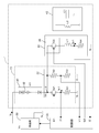
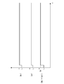
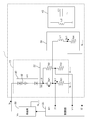
- Block diagram of LED backlight 10 Circuit diagram of parallel circuit H1 The flowchart which shows the control processing of the control part 24 Waveform diagram of driver current Id and shunt current Id Waveform diagram of driver current Id and shunt current Id Waveform diagram of driver current Id and shunt current Id Circuit diagram of parallel circuit H1
- LED backlight system an example of a light emitting device: hereinafter referred to as an LED backlight
- LED backlight a light emitting device
- the light-emitting device to which the present invention can be applied is not limited to this, and can also be applied to light-emitting devices used as various types of lighting and display devices.
- the LED backlight 10 includes a circuit unit 20, a supply unit 22, and a control unit 24.
- the circuit unit 20 includes four parallel circuits H1 to H4.
- the parallel circuits H1 to H4 are connected in parallel to each other, and the supply unit 22 supplies a supply voltage Vo common to the parallel circuits H1 to H4.
- the parallel circuit H1 includes a light emitting unit 30, a driving unit 32, a flow dividing unit 34, and a regenerating unit 40.
- the light emitting unit 30 and the driving unit 32 are connected in series to form a series circuit T1, and the supply voltage Vo is supplied to the series circuit T1. That is, it can be said that the supply unit 22 supplies the supply voltage Vo to the series circuit T1.
- the diversion unit 34 is connected in parallel to the drive unit 32 of the series circuit T1, and includes a diversion drive unit 36 therein.
- the regenerative unit 40 is connected to the flow dividing unit 34.
- the control unit 24 is connected to the supply unit 22 and controls the supply voltage Vo supplied by the supply unit 22.
- the control unit 24 is connected to the driving unit 32 and the diversion driving unit 34 of the parallel circuits H1 to H4 via separate wirings, and independently controls the driving unit 32 and the diversion unit 34.
- the parallel circuits H2 to H4 have the same configuration as the parallel circuit H1 except that the regenerative unit 40 is not provided, and the description thereof is omitted.
- FIG. 2 specifically shows the circuit configuration of the parallel circuit H1.
- the light emitting unit 30 includes a plurality of white LEDs (an example of a light emitting element) 42 connected in series.
- the LED 40 is designed so that the luminous efficiency is maximized when constant current control is performed. Therefore, the light emitting unit 30 is controlled so that the flowing current becomes a predetermined constant value Io. Further, in the LED 40, a forward voltage drop occurs due to current flowing, and a forward voltage Vf ⁇ b> 1 is generated in the light emitting unit 30.
- the forward voltage drop generated in the LED 42 is different for each LED 42, and the forward voltage Vf1 generated in the light emitting unit 30 is also different for each light emitting unit 30. Therefore, different drive unit voltages Vk1 to Vk4 are applied to the respective drive units 32 in the parallel circuits H1 to H4.
- the drive unit 32 includes a switching element Q1 (for example, an FET and other elements that perform a switching operation equivalent to this) and resistors R1 to R3.
- the switching element Q1 and the resistor R1 are connected in series between a connection point P to the light emitting unit 30 and a ground point G (that is, a connection point to the supply unit 22), and the resistors R2 and R3 are also connected to the connection point. It is connected in series between P and the ground point G.
- the resistors R2 and R3 are set to have higher resistance than the switching element Q1 and the resistor R1. Therefore, in the drive part 32, it is suppressed that an electric current flows through resistance R2 and resistance R3.
- the switching element Q1 is connected to the control terminal S1 of the control unit 24 and is controlled to be opened and closed by the control unit 24. As described above, in the drive unit 32, the current through the resistor R2 and the resistor R3 is suppressed, and the current flows through the switching element Q1 and the resistor R1. In the drive unit 32, the drive unit current Ik1 flows when the control unit 24 controls the switching element Q1 to “open”, and the drive unit current Ik1 stops when the control unit 24 controls the switching element Q1 to “close”. . That is, the switching element Q1 drives and controls the drive unit current Ik1 that flows through the drive unit 32 in cooperation with the control unit 24.
- the current detection terminal I1 of the control unit 24 is connected to an intermediate point between the switching element Q1 and the resistor R1, and detects the drive unit current Ik1 flowing through the drive unit 32. Further, the voltage detection terminal V1 of the control unit 24 is connected to an intermediate point between the resistors R2 and R3, and the drive unit voltage Vk1 applied to the connection point P is detected from the resistance ratio of the resistors R2 and R3. .
- the shunt unit 34 includes a switching element Q2, a coil L1, and a resistor R4, and these elements are connected in series between the connection point P and the ground point G in this order.
- the switching element Q ⁇ b> 2 is connected to the control terminal S ⁇ b> 2 of the control unit 24 and is controlled to be opened and closed by the control unit 24.
- the control unit 24 controls the switching element Q2 to be “open”, so that the shunt current Id1 flows.
- the control unit 24 controls the switching element Q2 to be “closed”, and the shunt current Id1 stops.
- the switching element Q2 functions as a shunt drive unit 36 that drives and controls the shunt current Id1 that flows through the shunt unit 34 in cooperation with the control unit 24. Further, the current detection terminal I2 of the control unit 24 is connected to an intermediate point between the coil L1 and the resistor R4, and detects the shunt current Id1 flowing through the shunt unit 36.
- the regeneration unit 40 has at least a coil L2 and a capacitor C1, and these elements are connected to each other.
- the coil L2 is sandwiched with respect to the coil L1 of the flow dividing section 34. Therefore, when a current flows through the coil L1, the coil L1 and the coil L2 are electrically or magnetically connected, a current flows through the coil L2, and as a result, electric power is stored in the capacitor C1.
- Control unit 24 The control unit 24 controls the switching element Q1 with respect to the parallel circuit H1, thereby controlling the driving unit current Ik1 flowing through the driving unit 32, and controlling the switching element Q2 with the shunting current Id1 flowing through the shunting unit 34. As a result, the current (Ik1 + Id1) flowing through the light emitting unit 30 is controlled. As described above, the amount of current flowing through the light emitting unit 30 needs to be controlled to a constant value Io. Therefore, when the control unit 24 controls the drive unit current Ik1 and the shunt current Id1, the control unit 24 adjusts the ratio of the drive unit current Ik1 and the shunt current Id1 while controlling the total amount to be a constant value Io. The amounts of the drive unit current Ik1 and the shunt current Id1 are determined.
- control unit 24 measures the drive unit current Ik1 and the shunt current Id1 through the current measurement terminals I1 and I2.
- the control unit 24 feeds back the measurement result to the control of the switching elements Q1 and Q2, thereby controlling the drive unit current Ik1 and the shunt current Id1 with high accuracy.
- the control unit 24 measures the drive unit voltage Vk1 through the voltage measurement terminal V1.
- the measurement result is fed back to the supply unit 22 to control the supply voltage Vo of the supply unit 22, thereby controlling the supply voltage Vo of the supply unit 22 with high accuracy in accordance with environmental conditions such as temperature. ing.
- control of the control unit 24 will be described with reference to FIG.
- the control unit 24 is connected to the parallel circuits H1 to H4 to detect the drive unit voltages Vk1 to Vk4, the drive unit currents Ik1 to Ik4, and the shunt currents Id1 to Id4 of each parallel circuit. It is used to control the drive unit 32, the diversion drive unit 36, and the supply unit 22 of each parallel circuit.
- the control unit 24 detects the drive unit voltages Vk1 to Vk4 of the parallel circuits H1 to H4 (step S2), and calculates the forward voltages Vf1 to Vf4 of each parallel circuit (step S4).
- the forward voltages Vf1 to Vf4 are determined based on the amount of current Io flowing through the light emitting unit 30, and are usually independent of the supply voltage Vo.
- the control unit 24 compares the calculated forward voltages Vf1 to Vf4 and selects the maximum forward voltage Vfmax (step S6).
- the forward voltages Vf1 to Vf4 satisfy the relationship of Vf1 ⁇ Vf2 ⁇ Vf3 ⁇ Vf4, and the control unit 24 selects Vf4 as the maximum forward voltage Vfmax.
- the control unit 24 determines the supply voltage Vo of the supply unit 22 based on the maximum forward voltage Vfmax (step S8).
- the drive unit 32 and the shunt unit 34 include elements such as a switch element Q and a resistor R, and the drive unit 32 needs to secure a minimum drive unit voltage Vkmin for operating these elements normally. There is.
- the control unit 24 calculates the supply voltage Vo from the maximum forward voltage Vfmax and the minimum drive unit voltage Vkmin. Therefore, if the voltage applied to the supply unit 30, the drive unit 32, and the flow dividing unit 34 is not insufficient, it is possible to suppress the excessive voltage from being applied to the drive unit 32 and the flow dividing unit 34.
- the control unit 24 determines the drive unit currents Ik1 to Ik3 so that the power P1 to P3 of the drive unit 32 of the parallel circuits H1 to H3 is equal to or lower than the power P4 of the drive unit 32 of the parallel circuit H4 (step). S14).
- the forward voltages Vf1 to Vf4 satisfy the relationship of Vf1 ⁇ Vf2 ⁇ Vf3 ⁇ Vf4.
- the control unit 24 needs to control the drive unit currents Ik1 to Ik3 so as to satisfy the relationship of Ik1 ⁇ Ik2 ⁇ Ik3 ⁇ Io. Control to satisfy the relationship. That is, the control unit 24 performs control so that a relatively large shunt current Id flows through the shunt unit 34 in the parallel circuits H1 to H4 in which the forward voltage Vf of the light emitting unit 30 is relatively small.
- FIG. 4 shows waveforms of the drive unit current Ik1, the shunt current Id1, and the current (Ik1 + Id1) flowing through the light emitting unit 30 in the parallel circuit H1.
- “H” indicates that the amount of current is large (high)
- “L” indicates that the amount of current is small (low).
- effective values of the currents flowing through the light emitting unit 30, the driving unit 32, and the shunt unit 34 are controlled. Therefore, as shown in FIG.
- the control unit 24 controls the switching element Q ⁇ b> 1 so that the effective value (dotted line) for each reference time of the drive unit current Ik ⁇ b> 1 flowing in the drive unit 32 is constant,
- the switching element Q2 is controlled so that the effective value (dotted line) of the flowing shunt current Id1 for each reference time is constant.
- the effective value (dotted line) of the current flowing through the light emitting unit 30 for each reference time is also controlled to a certain amount Io.
- the control is performed so that the shunt current Id1 is stopped when the drive section current Ik1 is passed, and the shunt current Id1 is passed when the drive section current Ik1 is stopped. Accordingly, it is possible to separate a period during which power is consumed by the drive unit 32 and a period during which power is regenerated by the regeneration unit 40. Therefore, for example, by synchronizing the on / off timing of the drive unit 32 with the blinking timing of the liquid crystal display device in which the LED backlight 10 is used, the regeneration unit 40 regenerates power during the non-display period of the liquid crystal display device. can do.
- the shunt unit 34 is connected in parallel to the drive unit 32 of the series circuits T1 to T4. Therefore, a part of the current flowing through the light emitting unit 30 can be diverted to the diverting unit 34, and the amount of the driving unit current Ik flowing through the driving unit 32 is suppressed to be smaller than the amount of current Io flowing through the light emitting unit 30. Can do. According to the LED backlight 10 of the present embodiment, even when an excess voltage equal to or higher than the minimum drive unit voltage Vkmin is applied to the drive unit 32, the amount of the drive unit current Ik flowing through the drive unit 32 is suppressed to a low level.
- the loss of the electric power P in the part 32 can be suppressed, and the temperature rise of the drive part 32 can be suppressed. As a result, it is not necessary to attach a heat radiating plate to suppress the temperature rise of the drive unit 32, or the size of the heat radiating plate can be reduced until it is not necessary. This simplifies the structure and reduces the manufacturing cost.
- a relatively large shunt current Id is set to flow through the shunt unit 34 connected to the series circuit T. That is, in the series circuit T in which a relatively large drive unit voltage Vk is applied to the drive unit 32, the drive unit 32 is set such that a relatively small drive unit current Ik flows.
- the loss of the electric power P in the drive part 32 can be suppressed, and the temperature rise of the drive part 32 can be suppressed.
- the regenerative unit 40 is provided in the parallel circuit H1, and the power P that has been lost by the drive unit 32 in the past can be stored in the regenerative unit 40. The loss of power P at 10 can be reduced.
- the control unit 24 shunts so as to prohibit the shunt current Id from flowing through the shunt unit 34 in the parallel circuit H4 where the forward voltage Vf of the light emitting unit 30 is maximized.
- the drive unit 36 is controlled.
- the minimum drive unit voltage Vkmin is applied to the drive unit 32, the loss of the electric power P4 in the drive unit 32 is small, the temperature rise in the drive unit 32 is low, and measures such as attaching a heat sink are not necessary.
- the control by the control unit 24 can be simplified by controlling the shunt drive unit 36 of the parallel circuit H4 as described above and not changing the opening and closing over time. it can.
- the drive unit current Ik1 and the shunt current Id1 are described using an example in which the variation is controlled over time.
- the present invention is not limited to this.
- the drive unit current Ik1 and the shunt current Id1 may be controlled to be constant values, as shown in FIG. 6, one of the drive unit current Ik1 and the shunt current Id1 is increased with time. Fluctuation control may be performed, and the other may be controlled to a constant value.
- the flow dividing unit 34 includes the flow dividing drive unit 36 and the flow dividing drive unit 36 is controlled by the control unit 24.
- the present invention is not limited to this. Absent.
- the shunting portion 34 is configured by a coil L1 and a resistor R4, and the shunting portion 34 is a part of the drive portion 32, that is, between the midpoint between the switching element Q1 and the resistor R1 and the ground point G. May be connected in parallel. As a result, the current flowing through the light emitting unit 30 can be controlled by the driving unit 32.
- the control in the control unit 24 can be simplified.
- the regeneration unit 40 includes the capacitor C1
- the present invention is not limited to this.
- the present invention is not limited to this.
- other light-emitting elements that can be used by adjusting the amount of current, such as a laser diode, may be used.
- a light emitting unit having a plurality of light emitting elements connected in series, and a driving unit connected to the plurality of light emitting elements in series to drive and control the light emitting unit.
- a shunt unit connected in parallel to the drive unit of the series circuit of the light emitting unit and the drive unit, and a supply unit for supplying a voltage to the series circuit, the shunt unit being connected
- a plurality of the series circuits are connected in parallel, and the supply unit applies the same voltage to each series circuit, and the current flowing through the light emitting units of each series circuit becomes a common constant value.
- the first forward voltage Vf1 of the first light emitting unit of the first series circuit is higher than the second forward voltage Vf2 of the second light emitting unit of the second series circuit. If small, connected to the first series circuit
- the first shunt portion and the second shunt portion connected to the second series circuit are such that the first shunt current Id1 flowing through the first shunt portion is larger than the second shunt current Id2 flowing through the second shunt portion.
- the driving unit in a series circuit in which a relatively large excess voltage is applied to the driving unit, the driving unit is set so that a relatively small current flows.
- the loss of power in the drive unit can be suppressed, and the effect of suppressing the temperature rise of the drive unit can be obtained.
Landscapes
- Engineering & Computer Science (AREA)
- Physics & Mathematics (AREA)
- Computer Hardware Design (AREA)
- General Physics & Mathematics (AREA)
- Theoretical Computer Science (AREA)
- Circuit Arrangement For Electric Light Sources In General (AREA)
- Led Devices (AREA)
Abstract
発光素子群の順方向電圧の差による駆動部の温度上昇を抑制する。本発明に係るLEDバックライト10は、直列に接続された複数のLED42を有する発光部30と、複数のLED42に直列に接続され、発光部30を駆動制御する駆動部32と、発光部30と駆動部32の直列回路T1のうち、駆動部32に対して並列に接続された分流部34と、直列回路T1に電圧を供給する供給部22を備える。このLEDバックライトによれば、発光部30に順方向電圧の差が生じた場合でも、駆動部32に流れる電流量を少なく抑えることで、駆動部32における電力の損失を抑えることができ、駆動部32の温度上昇を抑制することができる。
Description
本発明は、LED等の発光素子を備える発光装置に関する。
近年、発光素子にLED(Light Emitting Diode:発光ダイオード)等の半導体素子を用いた発光装置が普及しつつある。これらの発光装置は、初期駆動特性が優れ、振動やオン・オフ点灯の繰り返しに強いという特徴から液晶のバックライト用光源としての適用のための研究が進められている。
特許文献1に、これらの発光装置の回路構成の一例を示す。これらの発光装置では、従来のバックライト光源であるCCFL(Cold-Cathode Fluorescant Lamp:冷陰極蛍光灯)と異なる制御が必要であることから、発光装置の回路構成によっては電力損失が増大してしまうことがあった。電力損失が増大すると、電力の消費により発生する熱量が増大し、発光装置の温度が上昇してしまう。この場合には、発光装置の温度を抑制するための放熱板の取り付け等の対策が不可欠となる。
特許文献1に、発光装置の電力損失を低減する技術が開示されている。この技術では、発光素子を直列に接続した発光素子群の複数個を駆動させる回路において、各発光素子群における順方向電圧を検出し、複数の発光素子群に共通して印加する電圧を最適に調整することで、電力損失を低減するという。
(発明が解決しようとする課題)
しかし、特許文献1の技術を用いた場合でも、発光素子群の順方向電圧の差による電力損失を抑制することができない。発光素子群では、発光素子毎の順方向電圧のばらつきに起因して発光素子群毎の順方向電圧が異なる。そのため、複数の発光素子群に共通した電圧を印加する場合には、最大の順方向電圧に併せて調整された電圧が印加され、最大の順方向電圧を有しない発光素子群では、その発光素子群に直列に接続される駆動部に過剰電圧が印加される。また、各々の発光素子群に流れる電流は、駆動部によって共通の一定値となるように制御されており、発光素子群に直列に接続される駆動部にも一定の電流が流れる。この結果、最大の順方向電圧を有しない発光素子群に接続された駆動部では、過剰電圧の印加による電力損失を抑制することができず、局所的に温度が上昇してしまい、これらの駆動部の温度上昇を抑制する放熱板の取り付け等の対策が必要となる。
しかし、特許文献1の技術を用いた場合でも、発光素子群の順方向電圧の差による電力損失を抑制することができない。発光素子群では、発光素子毎の順方向電圧のばらつきに起因して発光素子群毎の順方向電圧が異なる。そのため、複数の発光素子群に共通した電圧を印加する場合には、最大の順方向電圧に併せて調整された電圧が印加され、最大の順方向電圧を有しない発光素子群では、その発光素子群に直列に接続される駆動部に過剰電圧が印加される。また、各々の発光素子群に流れる電流は、駆動部によって共通の一定値となるように制御されており、発光素子群に直列に接続される駆動部にも一定の電流が流れる。この結果、最大の順方向電圧を有しない発光素子群に接続された駆動部では、過剰電圧の印加による電力損失を抑制することができず、局所的に温度が上昇してしまい、これらの駆動部の温度上昇を抑制する放熱板の取り付け等の対策が必要となる。
本発明は、このような状況に鑑みてなされたものであり、発光素子群の順方向電圧の差による駆動部の温度上昇を抑制することを目的とする。
(課題を解決するための手段)
上記課題を解決するために、本発明の発光装置は、直列に接続された複数の発光素子を有する発光部と、前記複数の発光素子に直列に接続され、前記発光部を駆動制御する駆動部と、前記発光部と前記駆動部の直列回路のうち、前記駆動部に対して並列に接続された分流部と、前記直列回路に電圧を供給する供給部と、を備えることを特徴とする。
上記課題を解決するために、本発明の発光装置は、直列に接続された複数の発光素子を有する発光部と、前記複数の発光素子に直列に接続され、前記発光部を駆動制御する駆動部と、前記発光部と前記駆動部の直列回路のうち、前記駆動部に対して並列に接続された分流部と、前記直列回路に電圧を供給する供給部と、を備えることを特徴とする。
この発光装置では、分流部が直列回路の駆動部に並列に接続されている。そのため、発光部を流れた電流の一部を分流部に分流させることができ、駆動部を流れる電流量を、発光部を流れる電流量に比べて少なく抑えることができる。この発光装置によれば、駆動部に過剰電圧が印加される場合でも、駆動部を流れる電流量を少なく抑えることで、駆動部における電力の損失を抑えることができ、駆動部の温度上昇を抑制することができる。
本発明の発光装置では、前記分流部が接続された前記直列回路の複数個が並列に接続されているとともに、前記供給部は各直列回路に同一の電圧を印加しており、各直列回路の発光部に流れる電流が共通の一定値となるように駆動制御されている。この場合、第1直列回路の第1発光部の第1順方向電圧Vf1が第2直列回路の第2発光部の第2順方向電圧Vf2よりも小さい場合、前記第1直列回路に接続される第1分流部と前記第2直列回路に接続される第2分流部とは、前記第1分流部に流れる第1分流電流Id1が前記第2分流部に流れる第2分流電流Id2よりも大きくなるように設定されることが好ましい。
直列回路の複数個が並列に接続され、供給部から各直列回路に同一の電圧が印加される場合、各発光部の順方向電圧の差に起因して、各駆動部に過剰電圧が印加されることが多い。この発光装置では、発光部の順方向電圧が比較的小さく、駆動部に比較的大きな過剰電圧が印加される直列回路において、その直列回路に接続される分流部に比較的大きな分流電流が流れるように設定される。つまり、駆動部に比較的大きな過剰電圧が印加される直列回路において、その駆動部に比較的小さな電流が流れるように設定される。この発光装置によれば、駆動部における電力の損失を抑えることができ、駆動部の温度上昇を抑制することができる。
少なくとも1つの前記分流部は、当該分流部に流れる前記分流電流によって電力を蓄える回生部に接続されていることが好ましい。これによって、従来では駆動部によって損失されていた電力を回生部で蓄えることができ、発生装置における電力損失を低減することができる。
各分流部は、当該分流部に流れる前記分流電流を駆動制御する分流駆動部を有していることが好ましい。分流駆動部を有することで、分流部に流れる分流電流の量を制御することができ、その結果として、駆動部に流れる電流の量を適切に制御することができる。
前記駆動部と前記分流駆動部を制御する制御部をさらに備えることが好ましい。制御部が駆動部と分流駆動部を制御することで、発光部を流れる電流が制御されるとともに、駆動部と分流部の各々に流れる電流が制御される。この発光装置によれば、発光部に流れる電流の量の比を一定量に保つことができるとともに、駆動部と分流部に流れる電流の量を適切に調整することができる。
前記制御部は、各直列回路の駆動部に印加される駆動部電圧Vkと駆動部電流Ik、及び各直列回路に接続される分流部の前記分流電流Idを検出し、これらの検出結果に基づいて前記駆動部と前記分流駆動部を制御することが好ましい。これによって、発光部や駆動部、及び分流部に流れる電流の量を好適に調整することができる。
前記制御部は、前記複数の直列回路のうち、前記発光部の順方向電圧が最大となる直列回路に接続された分流部の分流駆動部が、当該分流部に前記分流電流が流れるのを禁止するように制御することが好ましい。
発光部の順方向電圧が最大となる直列回路では、この直列回路に基づいて供給部が供給する電圧が決められることから、一般に駆動部に過剰電圧が発生しないか、過剰電圧が低く抑えられている。そのため、この駆動部では、そもそも電力損失が少なく、駆動部の温度上昇を抑制する放熱板の取り付け等の対策が必要でないことが多い。この発光装置では、発光部の順方向電圧が最大となる直列回路において、分流部に分流電流が流れるのを禁止するように制御部が分流駆動部を制御する。この発光装置によれば、制御部における制御を簡略化することができる。
前記定電流発光素子は、LEDであることが好ましい。これによって、LEDを用いた発光装置において、LEDを駆動する駆動部の温度上昇を抑制することができる。
液晶表示装置用のバックライトであることが好ましい。これによって、駆動部の温度上昇が抑制された発光装置を液晶ディスプレイ用のバックライトとして用いることができる。すなわち、発光量が調整され、かつ局所的な発熱が抑制された好適なバックライトを実現することができる。
(発明の効果)
本発明によれば、発光素子群の順方向電圧の差による駆動部の温度上昇を抑制することができる。これによって、駆動部に対して放熱板の取り付け等の対策が不要となったり、また不要とならないまでも放熱板の大きさを縮小することができるようになり、発光装置の構造の簡略化及びコスト削減が実現される。
本発明によれば、発光素子群の順方向電圧の差による駆動部の温度上昇を抑制することができる。これによって、駆動部に対して放熱板の取り付け等の対策が不要となったり、また不要とならないまでも放熱板の大きさを縮小することができるようになり、発光装置の構造の簡略化及びコスト削減が実現される。
<実施形態>
本発明の一実施形態を、図面を参照して説明する。なお、以下の実施形態では、発光装置として液晶表示装置用のバックライトとして用いられるLEDバックライトシステム(発光装置の一例:以下、LEDバックライトと称する)10を用いて説明を行う。しかしながら、本発明が適用可能な発光装置はこれに限られるものではなく、各種照明や表示装置として使用される発光装置にも適用可能である。
本発明の一実施形態を、図面を参照して説明する。なお、以下の実施形態では、発光装置として液晶表示装置用のバックライトとして用いられるLEDバックライトシステム(発光装置の一例:以下、LEDバックライトと称する)10を用いて説明を行う。しかしながら、本発明が適用可能な発光装置はこれに限られるものではなく、各種照明や表示装置として使用される発光装置にも適用可能である。
1.LEDバックライトの構成
図1を用いて、LEDバックライト10の構成を説明する。
図1に示すように、LEDバックライト10は、回路部20と供給部22と制御部24を含んでいる。回路部20は、4つの並列回路H1~H4を備えている。並列回路H1~H4は、お互いに並列に接続されており、供給部22は、各並列回路H1~H4に共通した供給電圧Voを供給している。
図1を用いて、LEDバックライト10の構成を説明する。
図1に示すように、LEDバックライト10は、回路部20と供給部22と制御部24を含んでいる。回路部20は、4つの並列回路H1~H4を備えている。並列回路H1~H4は、お互いに並列に接続されており、供給部22は、各並列回路H1~H4に共通した供給電圧Voを供給している。
並列回路H1は、発光部30と駆動部32と分流部34と回生部40を含んでいる。発光部30と駆動部32は、直列に接続されて直列回路T1を形成しており、この直列回路T1に供給電圧Voが供給される。つまり、供給部22は、直列回路T1に供給電圧Voを供給しているということができる。分流部34は、直列回路T1の駆動部32に対して並列に接続されており、その内部に分流駆動部36を備えている。回生部40は、分流部34に接続されている。
制御部24は供給部22に接続されており、供給部22が供給する供給電圧Voを制御している。また制御部24は、並列回路H1~H4の駆動部32及び分流駆動部34に別々の配線を介して接続されており、駆動部32及び分流部34を各々独立して制御している。
なお、並列回路H2~H4は、回生部40を備えない他は並列回路H1と同一の構成をしており、その説明を省略する。
なお、並列回路H2~H4は、回生部40を備えない他は並列回路H1と同一の構成をしており、その説明を省略する。
図2に、並列回路H1の回路構成を具体的に示す。
(発光部30)
発光部30は、直列に接続された複数の白色LED(発光素子の一例)42を有している。一般に、LED40は、定電流制御された場合に発光効率が最大となるように設計されている。そのため、発光部30では、流れる電流が所定の一定値Ioとなるように制御されている。また、LED40では、電流が流れることで順電圧降下が発生し、発光部30に順方向電圧Vf1が発生する。そのため、駆動部32及び駆動部32に並列に接続される分流部36には、供給部22の供給電圧Voから発光部30の順方向電圧Vf1を減算した駆動部電圧Vk1(=Vo-Vf1)が印加される。
(発光部30)
発光部30は、直列に接続された複数の白色LED(発光素子の一例)42を有している。一般に、LED40は、定電流制御された場合に発光効率が最大となるように設計されている。そのため、発光部30では、流れる電流が所定の一定値Ioとなるように制御されている。また、LED40では、電流が流れることで順電圧降下が発生し、発光部30に順方向電圧Vf1が発生する。そのため、駆動部32及び駆動部32に並列に接続される分流部36には、供給部22の供給電圧Voから発光部30の順方向電圧Vf1を減算した駆動部電圧Vk1(=Vo-Vf1)が印加される。
一般に、LED42で発生する順電圧降下はLED42毎に異なり、発光部30に発生する順方向電圧Vf1も発光部30毎に異なる。そのため、並列回路H1~H4では、各々の駆動部32に異なる駆動部電圧Vk1~Vk4が印加される。
(駆動部32)
駆動部32は、スイッチング素子Q1(例えばFETであり、その他これと同等の切換動作を行う素子を含む。)と抵抗R1~R3を有している。スイッチング素子Q1と抵抗R1は、発光部30との接続点Pと接地点G(つまり、供給部22との接続点)との間に直列に接続されており、抵抗R2と抵抗R3も接続点Pと接地点Gとの間に直列に接続されている。抵抗R2及び抵抗R3は、スイッチング素子Q1及び抵抗R1よりも高抵抗に設定されている。そのため、駆動部32では、抵抗R2及び抵抗R3を介して電流が流れることが抑制されている。
駆動部32は、スイッチング素子Q1(例えばFETであり、その他これと同等の切換動作を行う素子を含む。)と抵抗R1~R3を有している。スイッチング素子Q1と抵抗R1は、発光部30との接続点Pと接地点G(つまり、供給部22との接続点)との間に直列に接続されており、抵抗R2と抵抗R3も接続点Pと接地点Gとの間に直列に接続されている。抵抗R2及び抵抗R3は、スイッチング素子Q1及び抵抗R1よりも高抵抗に設定されている。そのため、駆動部32では、抵抗R2及び抵抗R3を介して電流が流れることが抑制されている。
スイッチング素子Q1は、制御部24の制御端子S1に接続されており、制御部24によって開閉制御されている。上述したように、駆動部32では、抵抗R2及び抵抗R3を介した電流が抑制されており、スイッチング素子Q1及び抵抗R1を介して電流が流れる。駆動部32では、制御部24がスイッチング素子Q1を「開」に制御することで駆動部電流Ik1が流れ、制御部24がスイッチング素子Q1を「閉」に制御することで駆動部電流Ik1が止まる。すなわち、スイッチング素子Q1は、制御部24と共働して駆動部32に流れる駆動部電流Ik1を駆動制御している。
また、制御部24の電流検出端子I1がスイッチング素子Q1と抵抗R1の中間点に接続されており、駆動部32に流れる駆動部電流Ik1を検出している。また、制御部24の電圧検出端子V1が抵抗R2と抵抗R3の中間点に接続されており、抵抗R2と抵抗R3の抵抗比から接続点Pに印加される駆動部電圧Vk1を検出している。
(分流部34)
分流部34は、スイッチング素子Q2とコイルL1と抵抗R4を有しており、これらの素子はこの順に接続点Pと接地点Gとの間に直列に接続されている。スイッチング素子Q2は、制御部24の制御端子S2に接続されており、制御部24によって開閉制御されている。分流部34では、制御部24がスイッチング素子Q2を「開」に制御することで分流電流Id1が流れ、制御部24がスイッチング素子Q2を「閉」に制御することで分流電流Id1が止まる。すなわち、スイッチング素子Q2は、制御部24と共働して分流部34に流れる分流電流Id1を駆動制御する分流駆動部36として機能している。また、制御部24の電流検出端子I2がコイルL1と抵抗R4の中間点に接続されており、分流部36に流れる分流電流Id1を検出している。
分流部34は、スイッチング素子Q2とコイルL1と抵抗R4を有しており、これらの素子はこの順に接続点Pと接地点Gとの間に直列に接続されている。スイッチング素子Q2は、制御部24の制御端子S2に接続されており、制御部24によって開閉制御されている。分流部34では、制御部24がスイッチング素子Q2を「開」に制御することで分流電流Id1が流れ、制御部24がスイッチング素子Q2を「閉」に制御することで分流電流Id1が止まる。すなわち、スイッチング素子Q2は、制御部24と共働して分流部34に流れる分流電流Id1を駆動制御する分流駆動部36として機能している。また、制御部24の電流検出端子I2がコイルL1と抵抗R4の中間点に接続されており、分流部36に流れる分流電流Id1を検出している。
(回生部40)
回生部40は、少なくともコイルL2とコンデンサC1を有しており、これらの素子がお互いに接続されている。コイルL2は、分流部34のコイルL1に対して狭持されている。そのため、コイルL1に電流が流れることでコイルL1とコイルL2が電気あるいは磁気的に接続し、コイルL2に電流が流れ、その結果としてコンデンサC1に電力が蓄えられる。
回生部40は、少なくともコイルL2とコンデンサC1を有しており、これらの素子がお互いに接続されている。コイルL2は、分流部34のコイルL1に対して狭持されている。そのため、コイルL1に電流が流れることでコイルL1とコイルL2が電気あるいは磁気的に接続し、コイルL2に電流が流れ、その結果としてコンデンサC1に電力が蓄えられる。
(制御部24)
制御部24は、並列回路H1に対して、スイッチング素子Q1を制御することで駆動部32に流れる駆動部電流Ik1を制御し、スイッチング素子Q2を制御することで分流部34に流れる分流電流Id1を制御し、その結果として発光部30に流れる電流(Ik1+Id1)を制御している。上述したように、発光部30に流れる電流の量は一定値Ioに制御される必要がある。そのため、制御部24は、駆動部電流Ik1と分流電流Id1を制御する際に、その合計量が一定値Ioとなるように制御しつつ、駆動部電流Ik1と分流電流Id1の割合を調整し、駆動部電流Ik1と分流電流Id1の量を決定している。
制御部24は、並列回路H1に対して、スイッチング素子Q1を制御することで駆動部32に流れる駆動部電流Ik1を制御し、スイッチング素子Q2を制御することで分流部34に流れる分流電流Id1を制御し、その結果として発光部30に流れる電流(Ik1+Id1)を制御している。上述したように、発光部30に流れる電流の量は一定値Ioに制御される必要がある。そのため、制御部24は、駆動部電流Ik1と分流電流Id1を制御する際に、その合計量が一定値Ioとなるように制御しつつ、駆動部電流Ik1と分流電流Id1の割合を調整し、駆動部電流Ik1と分流電流Id1の量を決定している。
また、制御部24は電流測定端子I1、I2を介して駆動部電流Ik1と分流電流Id1を測定している。制御部24では、この測定結果をスイッチング素子Q1、Q2の制御にフィードバックさせることで、駆動部電流Ik1と分流電流Id1を高精度に制御している。また、制御部24は電圧測定端子V1を介して駆動部電圧Vk1を測定している。制御部24では、この測定結果を供給部22の供給電圧Voの制御に供給部22にフィードバックさせることで、温度等の環境条件に対応させて供給部22の供給電圧Voを高精度に制御している。
2.制御部の制御
図3を用いて、制御部24の制御について説明する。
制御部24は、並列回路H1~H4に接続して、各並列回路の駆動部電圧Vk1~Vk4、駆動部電流Ik1~Ik4、及び分流電流Id1~Id4を検出しており、これらの検出結果を用いて各並列回路の駆動部32や分流駆動部36、及び供給部22を制御している。なお、駆動部電流Ik1~Ik4と分流電流Id1~Id4は、以下の関係を満たすように制御される。
Ikn+Idn=Io(n=1~4)
図3を用いて、制御部24の制御について説明する。
制御部24は、並列回路H1~H4に接続して、各並列回路の駆動部電圧Vk1~Vk4、駆動部電流Ik1~Ik4、及び分流電流Id1~Id4を検出しており、これらの検出結果を用いて各並列回路の駆動部32や分流駆動部36、及び供給部22を制御している。なお、駆動部電流Ik1~Ik4と分流電流Id1~Id4は、以下の関係を満たすように制御される。
Ikn+Idn=Io(n=1~4)
まず制御部24は、並列回路H1~H4の駆動部電圧Vk1~Vk4を検出し(ステップS2)、各並列回路の順方向電圧Vf1~Vf4を算出する(ステップS4)。順方向電圧Vf1~Vf4は、発光部30に流れる電流の量Ioに基づいて決定され、通常、供給電圧Voに依存しない。順方向電圧Vf1~Vf4は、以下のように算出される。
Vfn=Vo-Vkn(n=1~4)
Vfn=Vo-Vkn(n=1~4)
次に制御部24は、算出された順方向電圧Vf1~Vf4を比較し、最大順方向電圧Vfmaxを選出する(ステップS6)。本実施形態では、順方向電圧Vf1~Vf4が、Vf1<Vf2<Vf3<Vf4の関係を満たしており、制御部24は最大順方向電圧VfmaxとしてVf4を選出する。
次に制御部24は、最大順方向電圧Vfmaxに基づいて供給部22の供給電圧Voを決定する(ステップS8)。駆動部32や分流部34にはスイッチ素子Qや抵抗R等の素子が含まれており、駆動部32では、これらの素子を正常に動作させるための最小駆動部電圧Vkminを確保しておく必要がある。制御部24は、最大順方向電圧Vfmaxと最小駆動部電圧Vkminから供給電圧Voを算出する。そのため、供給部30、駆動部32及び分流部34に印加される電圧が不足することも無ければ、駆動部32及び分流部34に過剰電圧が印加されることも抑制される。供給電圧Voを算出する式を以下に示す。
Vo=Vfmax+Vkmin
Vo=Vfmax+Vkmin
制御部24は、最大順方向電圧Vfmaxを有する並列回路H4の分流駆動部36を制御し、並列回路H4の分流部34に分流電流Id4が流れるのを禁止する(ステップS10)。また制御部24は、並列回路H4の駆動部32で消費される電力P4を算出する(ステップS12)。つまり、駆動部電流Ik4、分流電流Id4、及び電力P4は以下のように表される。
Ik4=Io、Id4=0、P4=Vk4×Ik4=(Vo-Vf4)×Io
Ik4=Io、Id4=0、P4=Vk4×Ik4=(Vo-Vf4)×Io
次に制御部24は、並列回路H1~H3の駆動部32の電力P1~P3が、並列回路H4の駆動部32の電力P4以下となるように、駆動部電流Ik1~Ik3を決定する(ステップS14)。並列回路H1~H3の駆動部32の電力P1~P3は、以下のように表される。
Pn=Vkn×Ikn=(Vo-Vfn)×Ikn(n=1~3)
Pn=Vkn×Ikn=(Vo-Vfn)×Ikn(n=1~3)
上述したように、本実施形態では、順方向電圧Vf1~Vf4は、Vf1<Vf2<Vf3<Vf4の関係を満たしている。そのため、制御部24は、駆動部電流Ik1~Ik3が、Ik1<Ik2<Ik3<Ioの関係を満たすように制御する必要があり、分流電流Id1~Id3についてみれば、Id1>Id2>Id3>0の関係を満たすように制御する。つまり、制御部24は、発光部30の順方向電圧Vfが比較的小さい並列回路H1~H4において、分流部34に比較的大きな分流電流Idが流れるように制御する。
3.駆動部電流及び分流電流の波形
図4に、並列回路H1における駆動部電流Ik1、分流電流Id1、及び発光部30に流れる電流(Ik1+Id1)の波形を示す。「H」は電流量が多い(ハイである)ことを示しており、「L」は電流量が少ない(ローである)ことを示している。並列回路H1~H4では、発光部30、駆動部32及び分流部34の各部を流れる電流が実効値制御されている。そのため制御部24は、図4に示すように、駆動部32に流れる駆動部電流Ik1の基準時間毎の実効値(点線)が一定となるようにスイッチング素子Q1を制御するとともに、分流部34に流れる分流電流Id1の基準時間毎の実効値(点線)が一定となるようにスイッチング素子Q2を制御する。これによって、発光部30に流れる電流の基準時間毎の実効値(点線)も一定量Ioに制御される。
図4に、並列回路H1における駆動部電流Ik1、分流電流Id1、及び発光部30に流れる電流(Ik1+Id1)の波形を示す。「H」は電流量が多い(ハイである)ことを示しており、「L」は電流量が少ない(ローである)ことを示している。並列回路H1~H4では、発光部30、駆動部32及び分流部34の各部を流れる電流が実効値制御されている。そのため制御部24は、図4に示すように、駆動部32に流れる駆動部電流Ik1の基準時間毎の実効値(点線)が一定となるようにスイッチング素子Q1を制御するとともに、分流部34に流れる分流電流Id1の基準時間毎の実効値(点線)が一定となるようにスイッチング素子Q2を制御する。これによって、発光部30に流れる電流の基準時間毎の実効値(点線)も一定量Ioに制御される。
本実施形態では、図4に示すように、駆動部電流Ik1を流す際には分流電流Id1を止め、駆動部電流Ik1を止める際には分流電流Id1を流すように制御を行っている。これによって、駆動部32で電力が消費される期間と、回生部40で電力が回生される期間を分離することができる。そのため、例えば駆動部32のオン/オフタイミングをLEDバックライト10が使用される液晶表示装置の点滅タイミングに同期させることで、液晶表示装置の非表示期間において回生部40が電力を回生する仕様とすることができる。
4.本実施形態の特徴
(1)本実施形態のLEDバックライト10では、並列回路H1~H4において、分流部34が直列回路T1~T4の駆動部32に並列に接続されている。そのため、発光部30を流れる電流の一部を分流部34に分流させることができ、駆動部32を流れる駆動部電流Ikの量を、発光部30を流れる電流の量Ioに比べて少なく抑えることができる。本実施形態のLEDバックライト10によれば、駆動部32に最小駆動部電圧Vkmin以上の過剰電圧が印加される場合でも、駆動部32を流れる駆動部電流Ikの量を少なく抑えることで、駆動部32における電力Pの損失を抑えることができ、駆動部32の温度上昇を抑制することができる。これによって、駆動部32の温度上昇を抑制するために放熱板を取り付ける必要が不要となったり、また不要とならないまでも放熱板の大きさを縮小することができるようになり、LEDバックライト10の構造が簡略化されるとともに、製造コストを削減することができる。
(1)本実施形態のLEDバックライト10では、並列回路H1~H4において、分流部34が直列回路T1~T4の駆動部32に並列に接続されている。そのため、発光部30を流れる電流の一部を分流部34に分流させることができ、駆動部32を流れる駆動部電流Ikの量を、発光部30を流れる電流の量Ioに比べて少なく抑えることができる。本実施形態のLEDバックライト10によれば、駆動部32に最小駆動部電圧Vkmin以上の過剰電圧が印加される場合でも、駆動部32を流れる駆動部電流Ikの量を少なく抑えることで、駆動部32における電力Pの損失を抑えることができ、駆動部32の温度上昇を抑制することができる。これによって、駆動部32の温度上昇を抑制するために放熱板を取り付ける必要が不要となったり、また不要とならないまでも放熱板の大きさを縮小することができるようになり、LEDバックライト10の構造が簡略化されるとともに、製造コストを削減することができる。
(2)本実施形態のLEDバックライト10では、並列回路H1~H4において、発光部30の順方向電圧Vfが比較的小さく、駆動部32に比較的大きな駆動部電圧Vkが印加される直列回路Tにおいて、その直列回路Tに接続される分流部34に比較的大きな分流電流Idが流れるように設定される。つまり、駆動部32に比較的大きな駆動部電圧Vkが印加される直列回路Tにおいて、その駆動部32に比較的小さな駆動部電流Ikが流れるように設定される。本実施形態のLEDバックライト10によれば、駆動部32における電力Pの損失を抑えることができ、駆動部32の温度上昇を抑制することができる。
(3)本実施形態のLEDバックライト10では、並列回路H1に回生部40を備えており、従来では駆動部32によって損失されていた電力Pを回生部40で蓄えることができ、LEDバックライト10における電力Pの損失を低減することができる。
(4)本実施形態のLEDバックライト10では、発光部30の順方向電圧Vfが最大となる並列回路H4において、分流部34に分流電流Idが流れるのを禁止するように制御部24が分流駆動部36を制御する。並列回路H4では、駆動部32に最小駆動部電圧Vkminが印加され、駆動部32における電力P4の損失も少なく、駆動部32における温度上昇も低く、放熱板の取り付け等の対策が必要でない。本実施形態のLEDバックライト10では、並列回路H4の分流駆動部36を上記のように制御し、時間の経過に伴って開閉を変化させないことで、制御部24による制御を簡略化することができる。
<他の実施形態>
本発明は上記記述及び図面によって説明した実施形態に限定されるものではなく、例えば次のような実施形態も本発明の技術的範囲に含まれる。
本発明は上記記述及び図面によって説明した実施形態に限定されるものではなく、例えば次のような実施形態も本発明の技術的範囲に含まれる。
(1)上記実施形態では、駆動部電流Ik1と分流電流Id1が時間の経過とともに変動制御される例を用いて説明したが、本発明はこれに限られない。図5に示すように、駆動部電流Ik1と分流電流Id1が各々一定値に制御されていてもよければ、図6に示すように、駆動部電流Ik1と分流電流Id1の一方が時間の経過とともに変動制御され、他方が一定値に制御されていてもよい。
(2)上記実施形態では、分流部34に分流駆動部36を備えており、制御部24によって分流駆動部36が制御される例を用いて説明を行ったが、本発明はこれに限られない。図7に示すように、分流部34がコイルL1と抵抗R4で構成されており、分流部34が駆動部32の一部、つまりスイッチング素子Q1と抵抗R1との中間点と接地点Gの間に並列に接続されていてもよい。これによって、発光部30に流れる電流を駆動部32によって制御することができる。また、並列回路H1~H4の発光部30の順方向電圧Vf1~Vf4に基づいて抵抗R1、R4とコイルL1を決定しておくことで、駆動部電流Ikと分流電流Idの比を調整することができ、制御部24における制御を簡略化することができる。
(3)上記実施形態では、回生部40にコンデンサC1を備える例を用いて説明を行ったが、本発明はこれに限られない。例えば、蓄電池等、電力を蓄える他の素子を備えていてもよい。
(4)上記実施形態では、発光素子としてLED42を用いて説明を行ったが、本発明はこれに限られない。例えば、レーザダイオード等、電流量が調整されて使用可能な他の発光素子が用いられてもよい。
本明細書または図面に説明した技術要素は、単独であるいは各種の組み合わせによって技術的有用性を発揮するものであり、出願時の請求項に記載の組み合わせやカテゴリに限定されるものではない。例えば、以下の方法も有用な技術である。
本明細書または図面に説明した発光装置の駆動方法では、直列に接続された複数の発光素子を有する発光部と、前記複数の発光素子に直列に接続され、前記発光部を駆動制御する駆動部と、前記発光部と前記駆動部の直列回路のうち、前記駆動部に対して並列に接続された分流部と、前記直列回路に電圧を供給する供給部と、を備え、前記分流部が接続された前記直列回路の複数個が並列に接続されているとともに、前記供給部は各直列回路に同一の電圧を印加しており、各直列回路の発光部に流れる電流が共通の一定値となるように駆動制御されている発光装置の駆動方法であり、第1直列回路の第1発光部の第1順方向電圧Vf1が第2直列回路の第2発光部の第2順方向電圧Vf2よりも小さい場合、前記第1直列回路に接続される第1分流部と前記第2直列回路に接続される第2分流部とは、前記第1分流部に流れる第1分流電流Id1が前記第2分流部に流れる第2分流電流Id2よりも大きくなるように設定する設定工程を備えている。
本明細書または図面に説明した発光装置の駆動方法によれば、駆動部に比較的大きな過剰電圧が印加される直列回路において、その駆動部に比較的小さな電流が流れるように設定されるので、駆動部における電力の損失を抑えることができ、駆動部の温度上昇を抑制する効果を得ることができる。
また、本明細書または図面に例示した技術は複数目的を同時に達成するものであり、そのうちの一つの目的を達成すること自体で技術的有用性を持つものである。
10…LEDバックライト、20…回路部、22…供給部、24…制御部、30…発光部、32…駆動部、34…分流部、36…分流駆動部、40…回生部、42…LED、H…並列回路、T…直流回路、Vf…順方向電圧、Vk…駆動部電圧、Ik…駆動部電流、Id…分流電流
Claims (9)
- 直列に接続された複数の発光素子を有する発光部と、
前記複数の発光素子に直列に接続され、前記発光部を駆動制御する駆動部と、
前記発光部と前記駆動部の直列回路のうち、前記駆動部に対して並列に接続された分流部と、
前記直列回路に電圧を供給する供給部と、
を備えることを特徴とする発光装置。 - 前記分流部が接続された前記直列回路の複数個が並列に接続されているとともに、前記供給部は各直列回路に同一の電圧を印加しており、
各直列回路の発光部に流れる電流が共通の一定値となるように駆動制御されており、
第1直列回路の第1発光部の第1順方向電圧Vf1が第2直列回路の第2発光部の第2順方向電圧Vf2よりも小さい場合、前記第1直列回路に接続される第1分流部と前記第2直列回路に接続される第2分流部とは、前記第1分流部に流れる第1分流電流Id1が前記第2分流部に流れる第2分流電流Id2よりも大きくなるように設定されることを特徴とする請求項1に記載の発光装置。 - 少なくとも1つの前記分流部は、当該分流部に流れる前記分流電流によって電力を蓄える回生部に接続されていることを特徴とする請求項2に記載の発光装置。
- 各分流部は、当該分流部に流れる前記分流電流を駆動制御する分流駆動部を有していることを特徴とする請求項2または3に記載の発光装置。
- 前記駆動部と前記分流駆動部を制御する制御部をさらに備えることを特徴とする請求項4に記載の発光装置。
- 前記制御部は、各直列回路の駆動部に印加される駆動部電圧Vkと駆動部電流Ik、及び各直列回路に接続される分流部の前記分流電流Idを検出し、これらの検出結果に基づいて前記駆動部と前記分流駆動部を制御することを特徴とする請求項5に記載の発光装置。
- 前記制御部は、前記複数の直列回路のうち、前記発光部の順方向電圧が最大となる直列回路に接続された分流部の分流駆動部が、当該分流部に前記分流電流が流れるのを禁止するように制御することを特徴とする請求項5または請求項6に記載の発光装置。
- 前記定電流発光素子は、LEDであることを特徴とする請求項1ないし請求項7のいずれか一項に記載の発光装置。
- 液晶表示装置用のバックライトであることを特徴とする請求項1ないし請求項8のいずれか一項に記載の発光装置。
Priority Applications (1)
| Application Number | Priority Date | Filing Date | Title |
|---|---|---|---|
| US13/811,795 US8970119B2 (en) | 2010-07-23 | 2011-06-15 | Light emitting device and method of controlling light emitting device |
Applications Claiming Priority (2)
| Application Number | Priority Date | Filing Date | Title |
|---|---|---|---|
| JP2010166261 | 2010-07-23 | ||
| JP2010-166261 | 2010-07-23 |
Publications (1)
| Publication Number | Publication Date |
|---|---|
| WO2012011339A1 true WO2012011339A1 (ja) | 2012-01-26 |
Family
ID=45496768
Family Applications (1)
| Application Number | Title | Priority Date | Filing Date |
|---|---|---|---|
| PCT/JP2011/063655 Ceased WO2012011339A1 (ja) | 2010-07-23 | 2011-06-15 | 発光装置 |
Country Status (2)
| Country | Link |
|---|---|
| US (1) | US8970119B2 (ja) |
| WO (1) | WO2012011339A1 (ja) |
Cited By (3)
| Publication number | Priority date | Publication date | Assignee | Title |
|---|---|---|---|---|
| WO2014008672A1 (zh) * | 2012-07-10 | 2014-01-16 | 深圳市华星光电技术有限公司 | 一种led背光驱动电路、背光模组和液晶显示装置 |
| CN106997747A (zh) * | 2017-05-27 | 2017-08-01 | 京东方科技集团股份有限公司 | 一种有机发光显示面板及显示装置 |
| JP2024530552A (ja) * | 2022-07-20 | 2024-08-23 | 綿陽恵科光電科技有限公司 | バックライト駆動回路、バックライトモジュール及び表示装置 |
Families Citing this family (2)
| Publication number | Priority date | Publication date | Assignee | Title |
|---|---|---|---|---|
| DE102015104973B3 (de) | 2015-03-31 | 2016-08-18 | Varroc Lighting Systems, s.r.o. | Anordnung und Verfahren zur Ansteuerung von mehreren in einer Reihenschaltung angeordneten Leuchtdioden |
| CN115035867B (zh) * | 2022-07-20 | 2023-04-28 | 绵阳惠科光电科技有限公司 | 背光驱动电路及方法、背光模组以及显示装置 |
Citations (1)
| Publication number | Priority date | Publication date | Assignee | Title |
|---|---|---|---|---|
| JP2003332623A (ja) * | 2002-05-07 | 2003-11-21 | Rohm Co Ltd | 発光素子駆動装置及び、発光素子を備えた電子機器 |
Family Cites Families (3)
| Publication number | Priority date | Publication date | Assignee | Title |
|---|---|---|---|---|
| JP2003332633A (ja) | 2002-05-16 | 2003-11-21 | Sony Corp | 表示装置および表示装置の製造方法 |
| JP4957024B2 (ja) | 2006-03-09 | 2012-06-20 | 日亜化学工業株式会社 | 発光装置、発光素子駆動回路及び発光素子の駆動方法 |
| US8334662B2 (en) * | 2009-09-11 | 2012-12-18 | Iwatt Inc. | Adaptive switch mode LED driver |
-
2011
- 2011-06-15 US US13/811,795 patent/US8970119B2/en not_active Expired - Fee Related
- 2011-06-15 WO PCT/JP2011/063655 patent/WO2012011339A1/ja not_active Ceased
Patent Citations (1)
| Publication number | Priority date | Publication date | Assignee | Title |
|---|---|---|---|---|
| JP2003332623A (ja) * | 2002-05-07 | 2003-11-21 | Rohm Co Ltd | 発光素子駆動装置及び、発光素子を備えた電子機器 |
Cited By (6)
| Publication number | Priority date | Publication date | Assignee | Title |
|---|---|---|---|---|
| WO2014008672A1 (zh) * | 2012-07-10 | 2014-01-16 | 深圳市华星光电技术有限公司 | 一种led背光驱动电路、背光模组和液晶显示装置 |
| CN106997747A (zh) * | 2017-05-27 | 2017-08-01 | 京东方科技集团股份有限公司 | 一种有机发光显示面板及显示装置 |
| CN106997747B (zh) * | 2017-05-27 | 2019-01-01 | 京东方科技集团股份有限公司 | 一种有机发光显示面板及显示装置 |
| US10950173B2 (en) | 2017-05-27 | 2021-03-16 | Ordos Yuansheng Optoelectronics Co., Ltd. | Organic light-emitting display panel and display device |
| JP2024530552A (ja) * | 2022-07-20 | 2024-08-23 | 綿陽恵科光電科技有限公司 | バックライト駆動回路、バックライトモジュール及び表示装置 |
| JP7639146B2 (ja) | 2022-07-20 | 2025-03-04 | 綿陽恵科光電科技有限公司 | バックライト駆動回路、バックライトモジュール及び表示装置 |
Also Published As
| Publication number | Publication date |
|---|---|
| US8970119B2 (en) | 2015-03-03 |
| US20130119873A1 (en) | 2013-05-16 |
Similar Documents
| Publication | Publication Date | Title |
|---|---|---|
| EP2177079B1 (en) | Self-powered led bypass-switch configuration | |
| JP5089193B2 (ja) | 発光装置 | |
| CN102640306B (zh) | Led驱动电路 | |
| CN103098236B (zh) | 照明装置用集成电路以及照明装置 | |
| US10152926B2 (en) | Driving circuit for light emitting element, light emitting device using same, and display apparatus | |
| US20020105373A1 (en) | LED drive circuit | |
| US9623791B2 (en) | Lighting device, vehicle illumination device, and vehicle | |
| JP2004253804A (ja) | 発光ダイオードの制御方法及び装置 | |
| CN101569236A (zh) | 用于使发光二极管的至少一个串联电路运行的触发装置和方法 | |
| JP2009035105A (ja) | 車両用灯具の点灯制御装置 | |
| WO2012011339A1 (ja) | 発光装置 | |
| JP5644420B2 (ja) | 発光ダイオード駆動装置 | |
| US9060405B2 (en) | Apparatus for controlling the operation of an LED, and method for controlling drive current thereof | |
| JP2014148253A (ja) | 駆動回路、車輌用灯具 | |
| JP5054236B1 (ja) | Led点灯装置 | |
| JP5214047B1 (ja) | Led点灯装置 | |
| EP3917285A1 (en) | Led system for vehicle lighting having high efficiency and high reliability | |
| JP2017033892A (ja) | 点灯回路、車両用灯具 | |
| WO2013046285A1 (ja) | 定電流駆動装置およびそれを用いた負荷駆動装置 | |
| CN105611688A (zh) | 一种led均流电路 | |
| JP5149457B1 (ja) | Led点灯装置 | |
| JP2014022196A (ja) | Led点灯装置 | |
| RU16028U1 (ru) | Сигнальное оптическое устройство | |
| KR101735813B1 (ko) | 엘이디 모듈 보호회로 | |
| JP6741914B2 (ja) | 半導体光源駆動装置 |
Legal Events
| Date | Code | Title | Description |
|---|---|---|---|
| 121 | Ep: the epo has been informed by wipo that ep was designated in this application |
Ref document number: 11809513 Country of ref document: EP Kind code of ref document: A1 |
|
| NENP | Non-entry into the national phase |
Ref country code: DE |
|
| WWE | Wipo information: entry into national phase |
Ref document number: 13811795 Country of ref document: US |
|
| 122 | Ep: pct application non-entry in european phase |
Ref document number: 11809513 Country of ref document: EP Kind code of ref document: A1 |
|
| NENP | Non-entry into the national phase |
Ref country code: JP |