WO2012011316A1 - バックライトユニットおよび液晶表示装置 - Google Patents
バックライトユニットおよび液晶表示装置 Download PDFInfo
- Publication number
- WO2012011316A1 WO2012011316A1 PCT/JP2011/061726 JP2011061726W WO2012011316A1 WO 2012011316 A1 WO2012011316 A1 WO 2012011316A1 JP 2011061726 W JP2011061726 W JP 2011061726W WO 2012011316 A1 WO2012011316 A1 WO 2012011316A1
- Authority
- WO
- WIPO (PCT)
- Prior art keywords
- light
- backlight unit
- guide plate
- light guide
- light source
- Prior art date
- Legal status (The legal status is an assumption and is not a legal conclusion. Google has not performed a legal analysis and makes no representation as to the accuracy of the status listed.)
- Ceased
Links
Images





Classifications
-
- G—PHYSICS
- G02—OPTICS
- G02B—OPTICAL ELEMENTS, SYSTEMS OR APPARATUS
- G02B6/00—Light guides; Structural details of arrangements comprising light guides and other optical elements, e.g. couplings
- G02B6/0001—Light guides; Structural details of arrangements comprising light guides and other optical elements, e.g. couplings specially adapted for lighting devices or systems
- G02B6/0011—Light guides; Structural details of arrangements comprising light guides and other optical elements, e.g. couplings specially adapted for lighting devices or systems the light guides being planar or of plate-like form
- G02B6/0033—Means for improving the coupling-out of light from the light guide
- G02B6/0035—Means for improving the coupling-out of light from the light guide provided on the surface of the light guide or in the bulk of it
- G02B6/0038—Linear indentations or grooves, e.g. arc-shaped grooves or meandering grooves, extending over the full length or width of the light guide
-
- G—PHYSICS
- G02—OPTICS
- G02F—OPTICAL DEVICES OR ARRANGEMENTS FOR THE CONTROL OF LIGHT BY MODIFICATION OF THE OPTICAL PROPERTIES OF THE MEDIA OF THE ELEMENTS INVOLVED THEREIN; NON-LINEAR OPTICS; FREQUENCY-CHANGING OF LIGHT; OPTICAL LOGIC ELEMENTS; OPTICAL ANALOGUE/DIGITAL CONVERTERS
- G02F1/00—Devices or arrangements for the control of the intensity, colour, phase, polarisation or direction of light arriving from an independent light source, e.g. switching, gating or modulating; Non-linear optics
- G02F1/01—Devices or arrangements for the control of the intensity, colour, phase, polarisation or direction of light arriving from an independent light source, e.g. switching, gating or modulating; Non-linear optics for the control of the intensity, phase, polarisation or colour
- G02F1/13—Devices or arrangements for the control of the intensity, colour, phase, polarisation or direction of light arriving from an independent light source, e.g. switching, gating or modulating; Non-linear optics for the control of the intensity, phase, polarisation or colour based on liquid crystals, e.g. single liquid crystal display cells
- G02F1/133—Constructional arrangements; Operation of liquid crystal cells; Circuit arrangements
- G02F1/1333—Constructional arrangements; Manufacturing methods
- G02F1/1335—Structural association of cells with optical devices, e.g. polarisers or reflectors
- G02F1/1336—Illuminating devices
- G02F1/133615—Edge-illuminating devices, i.e. illuminating from the side
-
- G—PHYSICS
- G02—OPTICS
- G02B—OPTICAL ELEMENTS, SYSTEMS OR APPARATUS
- G02B6/00—Light guides; Structural details of arrangements comprising light guides and other optical elements, e.g. couplings
- G02B6/0001—Light guides; Structural details of arrangements comprising light guides and other optical elements, e.g. couplings specially adapted for lighting devices or systems
- G02B6/0011—Light guides; Structural details of arrangements comprising light guides and other optical elements, e.g. couplings specially adapted for lighting devices or systems the light guides being planar or of plate-like form
- G02B6/0033—Means for improving the coupling-out of light from the light guide
- G02B6/0035—Means for improving the coupling-out of light from the light guide provided on the surface of the light guide or in the bulk of it
- G02B6/0036—2-D arrangement of prisms, protrusions, indentations or roughened surfaces
Definitions
- the present invention relates to a backlight unit that supplies light to a non-light-emitting display panel such as a liquid crystal display panel, and a liquid crystal display device including the backlight unit.
- a liquid crystal display device is often used as a display device for a monitor of a notebook computer, a television receiver or the like.
- the liquid crystal display device includes a liquid crystal panel and a backlight unit disposed on a back surface of the liquid crystal panel, and the liquid crystal panel adjusts a light transmittance (amount of transmission) from the backlight unit, and An image is displayed on the front of the LCD panel.
- backlight units There are two types of backlight units. One is a light guide plate method (edge light method) in which a light guide plate is used and light is incident from the side surface of the light guide plate, and the other is a direct type method in which a light source is arranged on the back surface of the liquid crystal module.
- a light guide plate method edge light method
- a direct type method in which a light source is arranged on the back surface of the liquid crystal module.
- FIG. 10 is a cross-sectional view of a conventional backlight unit.
- the backlight unit 92 includes a box-shaped backlight chassis 94 having an opening, a light guide plate 95 disposed in the backlight chassis 94, and the backlight chassis 94. And an LED lamp 96 which is a light source.
- the light guide plate 95 is a flat plate member made of a material that transmits light. As shown in FIG. 10, the light guide plate 95 is a light receiving portion 950 whose side receives light.
- the LED lamp 96 is disposed to face the light receiving unit 950 so as to emit light toward the light receiving unit 950.
- a surface adjacent to the light receiving unit 950 of the light guide plate 95 and facing the front is an emitting unit 953 that emits light. Light incident from the light receiving unit 950 spreads inside the light guide plate 95 while being reflected inside the light guide plate 95, and is emitted from the emission unit 953 as planar light.
- the light guide plate 95 is transparent in the vicinity of the light receiving unit 950, and a white pattern by printing is formed in a far part away from the light receiving unit 950. Due to the white pattern of the light guide plate 95, the light incident from the light receiving portion 950 into the light guide plate 95 is easily diffused. Thereby, the planar light emitted from the emission part 953 is made uniform (for example, refer to Japanese Patent Application Laid-Open No. 2010-113982).
- the light guide plate 95 is at least as thick as the light emitting portion of the LED lamp 96. Is needed. Thus, when the thickness of the light guide plate 95 is large, the weight of the light guide plate 95 increases, and the backlight unit 92 itself becomes heavy.
- an object of the present invention is to provide a backlight unit that can emit planar light that is lighter than conventional and has less luminance unevenness, and a liquid crystal display device using the backlight unit.
- the present invention provides a backlight unit including a light source and a light guide plate that receives light from the light source and emits the light as planar light, and the light guide plate is formed of a transparent thin plate. It is a corrugated sheet in which concave valleys and convex ridges are alternately arranged in a direction approaching and separating from the light source.
- the backlight unit can be made lightweight.
- the light guide plate is divided into a plurality of regions according to a distance from the light source, and the light guide plate has an uneven pitch that is an interval between the valley portions or the ridge portions in a region close to the light source.
- the pitch may be larger than the uneven pitch of the region far from the light source.
- the said light guide plate may be formed so large that the uneven
- the ratio of the valleys and the ridges for diffusing light is reduced, and the valleys for diffusing light in a part far from the light source to which some diffused light reaches.
- emitted from the said light-guide plate is equalized by increasing the ratio of the said ridge part.
- the said light source is arrange
- the light guide plate may have a shape in which two corrugated plates having different arrangement directions of the valley and the ridge are stacked.
- the light guide plate may be a triangular wave plate or a cosine wave (sine wave) wave plate.
- the structure which connected adjacent valley parts or ridge parts with a curved surface may be sufficient.
- a transparent thin plate on which dots are printed is folded to form a corrugated plate, and a transparent thin plate that is darkly colored with a colorant for light diffusion as the distance from the light source is folded to obtain a corrugated plate.
- fine irregularities and stripes (gratings) for diffusing light may be formed on the surface of a transparent thin plate formed on a corrugated plate.
- the present invention provides a backlight unit including a light source and a light guide plate that receives light from the light source and emits the light as planar light, and a plurality of the light guide plates are provided on an outer surface.
- the convex portions of the transparent thin plate are formed side by side in the vertical and horizontal directions, and the interval between the convex portions is wider as it is closer to the light source.
- the light guide plate is formed of a transparent thin plate, the light guide plate is lighter than a transparent light guide plate having the same thickness as the conventional light source.
- the backlight unit can be made lightweight.
- the light guide plate may be formed so that a front projection area of a convex portion far from the light source is small.
- the light source may include an LED lamp including one or two or more LED elements.
- a liquid crystal display device As an example of a device using the above-described backlight unit, a liquid crystal display device can be given.
- the present invention it is possible to provide a backlight unit that can emit planar light that is thinner and lighter than conventional ones and has less luminance unevenness, and a liquid crystal display device using the backlight unit.
- FIG. 3 is a cross-sectional view taken along line III-III of the backlight unit shown in FIG.
- FIG. 5 is a cross-sectional view of the light guide plate shown in FIG. 4 taken along line VV.
- FIG. 4 is a cross-sectional view of the light guide plate shown in FIG. 4 taken along line VV.
- FIG. 4 is a cross-sectional view of the light guide plate shown in FIG. 4 taken along line VV.
- FIG. 4 is a front view of the other example of the light-guide plate used for the backlight unit concerning this invention.
- It is the perspective view which expanded the part enclosed with the circle
- FIG. 1 is an exploded perspective view of an example of a liquid crystal display device including a backlight unit according to the present invention.
- the liquid crystal display device A includes a liquid crystal display panel 1 and a backlight unit 2 disposed on the back surface of the liquid crystal display panel 1.
- the liquid crystal display panel 1 includes a liquid crystal panel 11 in which liquid crystal is sealed, a polarizing plate 12 attached to the front surface (observer side) of the liquid crystal panel 11, and a rear surface of the liquid crystal panel 11 (backlight unit 2 side). And a polarizing plate 13 attached thereto.
- the liquid crystal panel 11 is filled between the array substrate including a switching element such as a TFT (thin film transistor), the counter substrate disposed opposite to the array substrate, on which a color filter is formed, and the array substrate and the counter substrate. Liquid crystal (both not shown).
- the liquid crystal panel 1 may have a configuration in which a color filter is formed on the array substrate and a transparent electrode is formed on the counter substrate.
- an optical sheet unit 3 is disposed between the liquid crystal display panel 1 and the backlight unit 2.
- the optical sheet unit 3 includes three optical sheets.
- the optical sheet unit 3 is not limited thereto, and may include more sheets or fewer sheets. It may be constituted by.
- the optical sheet unit 3 includes, for example, a diffusion sheet and a lens sheet.
- the diffusion sheet diffuses incident light inside. That is, the light incident on the diffusion sheet is diffused inside the diffusion sheet, and is emitted from the diffusion sheet as planar light with less luminance unevenness.
- the lens sheet is a sheet that deflects (condenses) light emission characteristics. When light is incident, the light is condensed and the light emission luminance per unit area is improved.
- optical sheets other than these may be used.
- the light emitted from the backlight unit 2 enters the optical sheet unit 3.
- the light incident on the optical sheet unit 3 is diffused or condensed to reduce the luminance unevenness and increase the light emission luminance and enter the liquid crystal display panel 1.
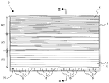
- FIG. 2 is a front view of the backlight unit used in the liquid crystal display device shown in FIG. 1, and FIG. 3 is a cross-sectional view of the backlight unit shown in FIG.
- the backlight unit 2 is an edge light type backlight.
- the backlight unit 2 includes a backlight chassis 4 that is a chassis, a light guide plate 5 that is held by the backlight chassis 4, and a plurality of light sources that are held by the backlight chassis 4. LED lamps 6 are provided. Between the light guide plate 5 and the backlight chassis 4, a reflection sheet 41 for reflecting light leaking from the back side of the light guide plate 5 and returning it to the light guide plate 5 is disposed.
- the light guide plate 5 is made of a light-transmitting material (for example, a transparent resin such as acrylic resin or PET) and has a rectangular shape in plan view.
- the light guide plate 5 is disposed inside the backlight chassis 4.
- the light guide plate 5 has one long side (the lower long side in FIG. 2) serving as the light receiving unit 50. Further, the light incident from the light receiving unit 50 is emitted from the emission unit 53 on the front side of the light guide plate 5.
- 15 LED lamps 6 are arranged close to the light receiving unit 50 of the light guide plate 5, but the present invention is not limited to this. Further, the LED lamp 6 may be provided with one LED element, and a plurality of LED elements (for example, LED elements that emit light of each wavelength of RGB) are combined into an LED lamp. There may be.
- the light guide plate 5 has a corrugated structure in which irregularities are formed by bending a transparent thin plate. More specifically, the light guide plate 5 has a corrugated structure in which concave valleys 51 and convex ridges 52 are alternately arranged as viewed from the front side (upper side in FIG. 3).
- the fold line (valley line) at the deepest part of the valley 51 and the fold line (ridge line) at the front side of the ridge 52 are parallel to each other.
- the valley line of the valley part 51 and the ridge line of the ridge part 52 are parallel to the long side of the light guide plate 5.
- the length between the valley lines of the adjacent valley portions 51 or the ridge line portions of the adjacent ridge portions 52 is set as the uneven pitch P, as the region A1 closest to the LED lamp 6, the farthest region A2, and the intermediate region A3.
- the valley 51 and the ridge 52 have an uneven pitch P1 in the region A1, an uneven pitch P3 in the region A3, and an uneven pitch P2 in the region A2.
- corrugated pitch has the relationship of P1> P3> P2.
- the light emitted from the LED lamp 6 is applied to the light receiving unit 50 of the light guide plate 5.
- the light irradiated to the light receiving part 50 is reflected by the surface of the valley part 51 or the ridge part 52 partially formed of a transparent resin, and the rest passes through the valley part 51 or the ridge part 52.
- the light transmitted through the valley 51 or the ridge 52 is further reflected or transmitted at the valley 51 or the ridge 52 away from the LED lamp 6.
- the light from the LED lamp 6 passes through the valley 51 or the ridge 52 while being partially reflected by the valley 51 or the ridge 52.
- the light guide plate 5 that is reflected to the front side by the plurality of valley portions 51 and the ridge portions 52 of the light guide plate 5 and is emitted from the emission portion 53 on the front side is formed in this manner, so that the light is moderately
- the light reaches the inside of the light guide plate 5 while being diffused. Since the light is emitted from the emission part 53 every time it passes through the valley part 51 or the ridge part 52, the light emitted from the emission part 53 becomes planar light.
- the light emitted to the back side is reflected by the reflection sheet 41 and enters the light guide plate 5 again.
- the light emitted from the reflection sheet 5 is applied to the valley portion 51 and the ridge portion 52 and reflected or transmitted. Thereby, the light radiate
- the concave / convex pitch of the valley portions 51 and the ridge portions 52 in the region away from the LED lamp 6 is narrow.
- the ratio of the light that is reflected by the valley portion 51 or the ridge portion 52 and emitted from the emission portion 53 on the front side is small.
- interval of the trough part 51 or the ridge part 52 is narrow, and the frequency
- the light guide plate 5 can equalize the luminance of the planar light emitted from the emitting portion 3 by adjusting the uneven pitch of the valley portions 51 and the ridge portions 52 (luminance unevenness). Can be suppressed).
- the light guide plate 5 Since the light guide plate 5 has a transparent thin plate corrugated structure, when emitting planar light that is equally uniform in the same area, it is lighter than a conventional light guide plate using a transparent flat plate. It is possible to create. Moreover, since the brightness unevenness of the planar light emitted from the emitting portion 53 can be adjusted with the uneven pitch, the light guide plate 5 can be easily designed.
- the light guide plate 5 is divided into a near area A1, a far area A2, and an intermediate area A3 depending on the distance from the LED lamp 6, and the uneven pitch P1 in the area A1 and the uneven pitch in the area A2.
- the uneven pitch P3 of P2 and the region A3 is formed so as to satisfy the relationship of P1> P3> P2, but is not limited to this. For example, it may be divided into two regions or may be divided into four or more regions. When the light guide plate is divided into a plurality of regions, it is only necessary that the uneven pitch in the region close to the LED lamp is wider than the far region.
- the light guide plate may be a single region so that the concave and convex pitches are equal over the entire surface.
- the valleys and ridges may be formed so as not to be divided into regions but to gradually become smaller as the uneven pitch is further away from the light source.
- the light guide plate 5 in which the valley line of the valley part 51 and the ridge line of the ridge part 52 are parallel to the long side of the backlight chassis 4 is cited, but the invention is not limited thereto.
- the valley line of the valley part 51 and the ridge line of the ridge part 52 may be inclined with respect to the long side of the backlight chassis 4.
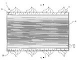
- FIG. 4 is a front view of another example of the light guide plate used in the backlight unit according to the present invention
- FIG. 5 is a cross-sectional view of the light guide plate shown in FIG. 4 taken along the line VV.
- the light guide plate 5 shown in FIGS. 4 and 5 has a configuration in which the light receiving units 50 are provided on both long sides, and the LED lamps 6 are arranged at positions close to the respective light receiving units 50.
- the concave / convex pitch P of the valley portion 51 and the ridge portion 52 of the light guide plate 5 is large at a position close to both the light receiving portions 50, and is at an intermediate portion between both light receiving portions 50 and 50. It is formed to be the smallest. Since the light guide plate 5 is formed in this way, light spreads inside the light guide plate 5 while being appropriately diffused. As a result, the light guide plate 5 can emit planar light with uniform luminance from the emitting portion 53. Moreover, since the LED lamp 6 irradiates the light guide plate 5 with light from two directions, the luminance level of the planar light emitted from the emitting portion 53 is increased as compared with the case where the light is emitted from one direction.
- the light guide plate 5 has a corrugated structure of a transparent thin plate, but is not limited thereto.
- a corrugated plate structure may be formed by bending a transparent thin plate on which dots are printed.
- a corrugated plate structure may be formed by bending a transparent thin plate that is deeply colored with a colorant for light diffusion as the distance from the LED lamp 6 increases.
- fine irregularities and stripes (gratings) for diffusing light may be formed on the surface of a transparent thin plate formed in a corrugated structure.
- the light guide plate 5 has a triangular corrugated wave plate structure, but is not limited to this, and may have a cosine wave (sine wave) wave plate structure.
- the structure which connected adjacent valley parts or ridge parts with a curved surface may be sufficient.
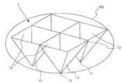
- FIG. 6 is a front view of another example of the light guide plate used in the backlight unit according to the present invention
- FIG. 7 is an enlarged perspective view of a circled portion of the light guide plate shown in FIG.
- the light guide plate 7 includes a valley portion 71 and a ridge portion 72 parallel to the long side, and a valley portion 73 and a ridge portion 74 parallel to the short side.
- the valley 71, the valley 73, and the ridge 74, and the ridge 72, the valley 73, and the ridge 74 are orthogonal to each other.
- the light incident from the light receiving portion 701 having a long rectangular shape is reflected by the trough portion 71 and the ridge portion 72 or transmitted through the trough portion 71 and the ridge portion 72, and is appropriately diffused while being diffused. 5 inside.
- light incident from the light receiving portion 702 having a short side is reflected by the valley portion 73 and the ridge portion 74 or transmitted through the valley portion 73 and the ridge portion 74, and reaches the inside of the light guide plate 5 while being appropriately diffused.
- the light emitted from the LED lamp 6 is diffused moderately and reaches the inside of the light guide plate 5, so that the planar light with uniform luminance is emitted from the emission part 73.
- the LED lamp 6 irradiates the light guide plate 7 with light from four directions, the luminance level of the planar light emitted from the emission unit 73 is increased as compared with other cases.
- the light guide plate 7 is formed so that the concave and convex pitches of the valley portions 71 and the ridge portions 72 and the concave and convex pitches of the valley portions 73 and the ridge portions 74 are constant in all regions, but become smaller toward the center. Good.
- both the long side and the short side are the light receiving unit 70, but the light receiving unit 70 is not limited thereto, and only one of the long side or the short side is the light receiving unit. Only one of the long sides and one of the short sides may be the light receiving unit. In the case of this configuration, the valley and the ridge may be formed so that the uneven pitch becomes narrower as the opposing sides are separated from the light receiving unit that is not the light receiving unit.
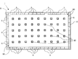
- FIG. 8 is a front view of still another example of the light guide plate used in the backlight unit according to the present invention
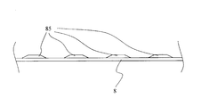
- FIG. 9 is an enlarged view of the light guide plate shown in FIG.
- the light guide plate 8 is a transparent thin plate, and square frustum-shaped convex portions 85 are arranged vertically and horizontally on the front side of the light guide plate 8. Further, all four sides of the light guide plate 8 serve as the light receiving unit 80, and the LED lamp 6 is disposed in the vicinity of the light receiving unit 80. The light emitted from the LED lamp 6 is reflected by the convex portion 85 or transmitted through the convex portion 85. As shown in FIG. 8, the interval between the convex portions 85 is wide at the edge of the light guide plate 8, that is, the portion close to the LED lamp 6, and the interval between the convex portions 85 is narrow at the central portion.
- the light guide plate 8 can emit the planar light with uniform luminance from the emitting portion 83.
- the convex portion 85 has a quadrangular frustum shape, but is not limited thereto, and a shape capable of diffusing light, such as a hemispherical shape, a conical shape, a truncated cone shape, and an elongated shape. Can be widely adopted. Further, the convex portion 85 may have a smaller front projection area toward the center. In this way, the light guide plate 8 can increase the uniformity of the planar light emitted from the emission part 83 by adjusting the size and the arrangement interval.
- the present invention can be used as a display device for devices such as a thin television device, a thin display device, and a mobile phone.
Landscapes
- Physics & Mathematics (AREA)
- General Physics & Mathematics (AREA)
- Optics & Photonics (AREA)
- Nonlinear Science (AREA)
- Mathematical Physics (AREA)
- Chemical & Material Sciences (AREA)
- Crystallography & Structural Chemistry (AREA)
- Planar Illumination Modules (AREA)
Abstract
従来よりも薄型、軽量であるとともに、輝度むらの少ない面状光を出射できるようにするため、バックライトユニット2において、導光板5が、透明薄板で形成されており、光源6に対して接近離間する方向に、凹形状の谷部51と凸形状の稜部52とが交互に配列された波板とした。
Description
本発明は、液晶表示パネルのような非発光型表示パネルに光を供給するバックライトユニット、およびそれを備える液晶表示装置に関するものである。
近年、ノートパソコンのモニタ、テレビジョン受像機等の表示装置として液晶表示装置が採用されていることが多い。前記液晶表示装置は、液晶パネルと、液晶パネルの背面に配置されるバックライトユニットを備えており、前記液晶パネルが、前記バックライトユニットからの光の透過率(透過量)を調整し、前記液晶パネルの前面に画像を表示している。
前記バックライトユニットには、大きく分けて2種類ある。1つは、導光板を用い、前記導光板の側面から光を入射させる導光板方式(エッジライト方式)であり、もう1つは液晶モジュールの背面に光源を配置した直下型方式である。前記液晶表示装置に対する薄型化及び小型化の要求が高まっており、直下型方式に比べ、薄いエッジライト方式のバックライトユニットを採用する液晶表示装置が多くなっている。また、近年、前記バックライトユニットの光源としてLED素子を備えるLEDランプが用いられることが多くなってきている。
従来のバックライトユニットについて図面を参照して説明する。図10は従来のバックライトユニットの断面図である。図10に示すように、バックライトユニット92は、開口を有する箱型のバックライトシャーシ94と、バックライトシャーシ94の内部に配置された導光板95と、前記バックライトシャーシ94の内部に配置された光源であるLEDランプ96とを備えている。
導光板95は光が透過する材料で形成された平板状の部材である。図10に示すように、導光板95は側面が光を受け入れる受光部950となっている。LEDランプ96は受光部950に向かって光を出射するように、受光部950と対向して配置されている。そして、導光板95の受光部950と隣り合う面であって、正面に向いている面が光を出射する出射部953となっている。受光部950より入射した光は、導光板95の内部で反射しつつ導光板95の内部を広がり、出射部953から面状光として出射される。
図10に示すバックライトユニット92では、導光板95は受光部950の近傍は透明で、受光部950から遠ざかる遠い部分には印刷による白色パターンが形成されている。導光板95の白色パターンによって、受光部950から導光板95の内部に入射した光が拡散しやすくなっている。これにより、出射部953より出射される面状光が均一化される(例えば、特開2010-113982号公報参照)。
しかしながら、図10に示すように、従来のバックライトユニット92では、導光板95の内部で光を拡散させているので、導光板95は少なくともLEDランプ96の光を出射する部分の厚さと同じ厚さが必要となっている。このように、導光板95の厚さが厚いと、導光板95の重量がかさみ、バックライトユニット92自体も重くなってしまう。
そこで本発明は、従来よりも軽量であるとともに、輝度むらの少ない面状光を出射できるバックライトユニット及びそのバックライトユニットを用いた液晶表示装置を提供することを目的とする。
上記目的を達成するために本発明は、光源と、前記光源からの光を受光し面状光として出射する導光板とを備えたバックライトユニットであって、前記導光板は、透明薄板で形成されており、前記光源に対して接近離間する方向に、凹形状の谷部と凸形状の稜部とが交互に配列された波板であることを特徴とする。
この構成によると、前記光源からの光は一部が前記谷部及び前記稜部で正面側に反射されるとともに、残りが前記谷部及び前記稜部を透過する。これにより、前記光源からの光は、拡散されつつ前記導光板内に広がるので、前記導光板より出射される前記面状光の輝度を均一化することができる。また、前記導光板は、透明薄板の波型形状であるので、従来のような前記光源の厚さ(大きさ)と同じ厚さを有する透明板状の導光板に比べて軽量である。このことより、前記バックライトユニットを軽量に作成することが可能である。
上記構成において、前記導光板は前記光源からの距離によって複数の領域に分割されており、前記導光板は、前記光源に近い領域の前記谷部同士又は前記稜部同士の間隔である凹凸ピッチが、前記光源から遠い領域の前記凹凸ピッチよりも大きく形成されていてもよい。また、前記導光板は、前記谷部同士又は前記稜部同士の間隔である凹凸ピッチが、前記光源に近いほど大きく形成されていてもよい。
この構成によると、光量が大きい光源の近傍では、光を拡散させる前記谷部及び前記稜部の割合を減らし、ある程度拡散された光が到達する光源よりも遠い部分では光を拡散させる前記谷部及び前記稜部の割合を増やすことで、前記導光板より出射される面状光の輝度が均一化される。
上記構成において、前記光源が、前記導光板を挟んで対向するように配置されており、前記導光板は、前記谷部同士又は前記稜部同士の感覚である凹凸ピッチが、前記対を成す光源の中間部分で最も狭くなるように構成されていてもよい。この構成によると、前記導光板は、前記導光板より出射される面状光の輝度むらを抑制しつつ、輝度レベルを上げることができる。
上記構成において、前記導光板は、前記谷部及び前記稜部の配列方向が異なる2系統の波板を重ねた形状を有していてもよい。
さらに上記構成において、前記導光板は、三角波形状の波板ってもよく、余弦波(正弦波)形状の波板であってもよい。また、隣り合う谷部同士或いは稜部同士を曲面でつないだ構造であってもよい。
さらに上記構成において、前記導光板として、ドットを印刷した透明薄板を折り曲げて波板としたもの、前記光源から遠ざかるほど光拡散用の着色剤で濃く着色された透明薄板を折り曲げて波板としたもの、さらには、波板に形成した透明薄板の表面に光を拡散させるための微少な凹凸や縞(グレーティング)を形成したものであってもよい。
上記目的を達成するために本発明は、光源と、前記光源からの光を受光し面状光として出射する導光板とを備えたバックライトユニットであって、前記導光板は、外面に複数個の凸部が縦横に並んで形成された透明薄板であり、前記凸部同士の間隔が、前記光源に近いほど広いことを特徴とする。
この構成によると、前記導光板が透明薄板で形成されているので、従来のような前記光源の厚さ(大きさ)と同じ厚さを有する透明板状の導光板に比べて軽量である。このことより、前記バックライトユニットを軽量に作製することが可能である。
上記構成において、前記導光板は、前記光源より遠い部分の凸部の正面投影面積が小さくなるように形成されていてもよい。
上記構成において、前記光源として、1又は2以上のLED素子を含むLEDランプを挙げることができる。
上述のバックライトユニットを利用した機器の例として、液晶表示装置を挙げることができる。
本発明によると、従来よりも薄型、軽量であるとともに、輝度むらの少ない面状光を出射できるバックライトユニット及びそのバックライトユニットを用いた液晶表示装置を提供することができる。
以下に本発明の実施形態について図面を参照して説明する。図1は本発明にかかるバックライトユニットを備えている液晶表示装置の一例の分解斜視図である。図1に示すように、液晶表示装置Aは、液晶表示パネル1と、液晶表示パネル1の背面に配置されたバックライトユニット2とを含んでいる。
液晶表示パネル1は、液晶が封入された液晶パネル11と、液晶パネル11の前面(観察者側)に貼り付けられた偏光板12と、液晶パネル11の後面(バックライトユニット2側)に貼り付けられた偏光板13とを有している。液晶パネル11は、TFT(薄膜トランジスタ)等のスイッチング素子を含むアレイ基板と、アレイ基板と対向して配置され、カラーフィルタが形成された対向基板と、アレイ基板と対向基板との間に充填される液晶とを含んでいる(いずれも不図示)。なお、液晶パネル1は、カラーフィルタが前記アレイ基板に形成され、前記対向基板には透明電極が形成されている構成であってもよい。
図1に示すように、液晶表示装置Aには、液晶表示パネル1とバックライトユニット2との間に、光学シートユニット3が配置されている。図1に示す液晶表示装置Aにおいて、光学シートユニット3は3枚の光学シートを備えているが、それに限定されるものではなく、より多くのシートを含むものであっても、或いは、少ないシートで構成されるものであってもよい。光学シートユニット3には、例えば、拡散シートやレンズシートなどが含まれている。拡散シートは入射された光を内部で拡散する。すなわち、拡散シートに入射した光は、拡散シート内部で拡散し、輝度むらの少ない面状光として拡散シートから出射される。レンズシートは光の放射特性を偏向させる(集光させる)シートであり、光が入射すると、その光は集光され、単位面積あたりの発光輝度が向上する。なお、これら以外の光学シートが用いられることもある。
バックライトユニット2から出射した光は、光学シートユニット3に入射する。光学シートユニット3に入射した光は拡散されたり、集光されたりして、輝度むらを減らすとともに、発光輝度を高め、液晶表示パネル1に入射する。
バックライトユニット2について図面を参照して詳しく説明する。図2は図1に示す液晶表示装置に用いられるバックライトユニットの正面図であり、図3は図2に示すバックライトユニットのIII-III線で切断した断面図である。バックライトユニット2はエッジライト式のバックライトである。図2、図3に示すように、バックライトユニット2は、シャーシであるバックライトシャーシ4と、バックライトシャーシ4に保持された導光板5と、バックライトシャーシ4に保持された光源である複数個のLEDランプ6とを備えている。導光板5とバックライトシャーシ4との間には、導光板5の背面側から漏れた光を反射し、導光板5に戻すための反射シート41が配置されている。
導光板5は光が透過する材料(例えば、アクリル樹脂やPET等の透明な樹脂)で作製され、平面視長方形状を有している。導光板5はバックライトシャーシ4の内部に配置されている。導光板5は一方の長辺(図2において下側の長辺)が受光部50となっている。また、受光部50から入射された光は導光板5の正面側の出射部53から出射される。なお、バックライトユニット2では、導光板5の受光部50に近接してLEDランプ6が15個配置されているが、これに限定されるものではない。また、LEDランプ6はLED素子を1個備えているものであってもよく、複数個のLED素子(例えば、RGBそれぞれの波長の光を出射するLED素子)をまとめてLEDランプとしたものであってもよい。
図2、3に示すように、導光板5は透明薄板を折り曲げて凹凸を形成した波板構造を有している。詳しく説明すると、導光板5は正面側(図3において上側)から見て凹形状の谷部51と凸形状の稜部52とが交互に並んだ波板構造である。そして、谷部51の最も深い部分の折れ線(谷線)と稜部52の最も正面側の折れ線(稜線)とは互いに平行である。また、谷部51の谷線及び稜部52の稜線は導光板5の長辺と平行となっている。
導光板5では、LEDランプ6に最も近い領域A1、最も遠い領域A2、中間領域A3とし、隣り合う谷部51の谷線同士或いは隣り合う稜部52の稜線部同士の長さを凹凸ピッチPとする。図3に示すように、谷部51及び稜部52は、領域A1で凹凸ピッチP1、領域A3では凹凸ピッチP3、領域A2では凹凸ピッチP2となっている。そして、導光板5では凹凸ピッチがP1>P3>P2の関係となっている。
次に、バックライトユニット2の動作について説明する。まず、LEDランプ6から出射された光は、導光板5の受光部50に照射される。受光部50に照射された光は、一部が透明樹脂で形成された谷部51又は稜部52の表面で反射され、残りは谷部51又は陵部52を透過する。谷部51又は陵部52を透過した光は、さらにLEDランプ6から離れた谷部51又は陵部52において、反射又は透過する。
このように、LEDランプ6からの光は、一部が谷部51又は陵部52で反射されつつ、谷部51又は陵部52を透過する。導光板5の複数個の谷部51及び陵部52で正面側に反射され、正面側の出射部53から出射される導光板5が、このように形成されていることで、光は適度に拡散されつつ導光板5の内部にいきわたる。そして、光は、谷部51又は稜部52を透過するたびに、出射部53から出射されるので、出射部53から出射される光は面状光になる。
また、背面側に出射された光は、反射シート41で反射され、再度、導光板5に入射する。反射シート5で出射された光は谷部51及び陵部52に照射され、反射又は透過する。これにより、背面側に出射された光を有効に利用することができる。
導光板5において、LEDランプ6から離れた領域の谷部51及び陵部52の凹凸ピッチが狭くなっている。このことにより、LEDランプ6から近い領域では、谷部51又は陵部52で反射され正面側の出射部53から出射される光の割合が少ない。逆に、LEDランプ6から遠い部分では、谷部51又は陵部52の間隔が狭く、光が透過及び反射を繰り返す回数が増える。
そして、LEDランプ6から遠い領域(領域A1に対する領域A2、A3、領域A3に対する領域A2)では、透過を繰り返す毎に、正面側の出射部53から光が出射され、LEDランプ6の近傍の領域に比べて、透過する光量が少なくなっている。つまり、LEDランプ6から近い部分では光量が多いが、谷部51及び稜部52で透過/反射される回数が少ない。逆に遠い部分では光量は少ないが、谷部51及び稜部52で透過/反射される回数が多い。これにより、導光板5において、谷部51及び稜部52の凹凸ピッチを調整すれば、導光板5は、出射部3から出射される面状光の輝度を均一化することができる(輝度むらを抑えることができる)。
導光板5が透明薄板の波板構造であるので、同じ面積で同等に均一化された面状光を出射する場合、従来の透明な板状の平板を用いた導光板にくらべて、軽量に作成することが可能である。また、出射部53から出射される面状光の輝度むらの調整を凹凸ピッチで行うことができるので、導光板5の設計が容易である。
なお、上述の実施形態において、導光板5は、LEDランプ6からの距離によって近い領域A1、遠い領域A2、中間の領域A3に分けられており、領域A1の凹凸ピッチP1、領域A2の凹凸ピッチP2及び領域A3の凹凸ピッチP3には、P1>P3>P2の関係が成り立つように形成されていたが、これに限定されるものではない。たとえば、2つの領域に分けてもよく、4以上の領域に分けてもよい。導光板を複数の領域に分割したとき、LEDランプに近い領域の凹凸ピッチが遠い領域よりも広くなるように形成されていればよい。
なお、導光板をひとつの領域とし、全面で凹凸ピッチが等しくなるようにしてもよい。或いは、領域に分割せず、凹凸ピッチが光源より遠ざかることで徐々に小さくなるように谷部及び稜部が形成されていてもよい。さらに、バックライトユニット2では、谷部51の谷線及び稜部52の稜線がバックライトシャーシ4の長辺と平行となっている導光板5を挙げているが、これに限定されるものではなく、谷部51の谷線及び稜部52の稜線がバックライトシャーシ4の長辺に対して傾いていてもよい。
本発明にかかるバックライトユニットの他の例について図面を参照して説明する。図4は本発明にかかるバックライトユニットに用いられる導光板の他の例の正面図であり、図5は図4に示す導光板をV-V線で切断したときの断面図である。図4、図5に示す導光板5は、両方の長辺に受光部50を備えた構成であり、各受光部50の近接した位置に、LEDランプ6が配置されている。
図4、図5に示すように、導光板5の谷部51及び稜部52の凹凸ピッチPは、両方の受光部50に近い位置では、大きく、両方の受光部50、50の中間部分で最も小さくなるように形成されている。導光板5が、このように形成されていることで、光は適度に拡散されつつ導光板5の内部にいきわたる。これにより、導光板5は輝度が均一化された面状光を出射部53から出射することが可能である。また、LEDランプ6が2方向から導光板5に光を照射するので、一方向から照射される場合に比べて、出射部53から出射される面状光の輝度レベルが上がる。
以上の説明において、導光板5として、透明薄板の波板構造のものを用いているが、それに限定されるものではない。例えば、ドットを印刷した透明薄板を折り曲げて波板構造としたものであってもよい。また、LEDランプ6から遠ざかるほど光拡散用の着色剤で濃く着色された透明薄板を折り曲げて波板構造としたものであってもよい。さらには、波板構造に形成した透明薄板の表面に光を拡散させるための微少な凹凸や縞(グレーティング)を形成したものであってもよい。また、導光板5は三角波形の波板構造を有しているが、これに限定されるものではなく、余弦波(正弦波)形状の波板構造であってもよい。また、隣り合う谷部同士或いは稜部同士を曲面でつないだ構造であってもよい。
本発明にかかるバックライトユニットの他の例について図面を参照して説明する。図6は本発明にかかるバックライトユニットに用いられる導光板の他の例の正面図であり、図7は図6に示す導光板の円で囲んだ部分を拡大した斜視図である。
図6に示すように、導光板7は長方形状の4辺の全てが受光部70となっており、LEDランプ6が各受光部70の近傍に配置されている。図6に示すように、導光板7は長辺と平行な谷部71及び稜部72と、短辺と平行な谷部73及び稜部74とを備えている。谷部71と谷部73及び稜部74、稜部72と谷部73及び稜部74が直交している。
導光板7では、長方形状の長辺である受光部701から入射された光は、谷部71及び稜部72で反射又は谷部71及び稜部72を透過し、適度に拡散されつつ導光板5の内部にいきわたる。また、短辺である受光部702から入射された光は、谷部73及び稜部74で反射又は谷部73及び稜部74を透過し、適度に拡散されつつ導光板5の内部にいきわたる。これにより、LEDランプ6から出射された光は適度に拡散されつつ導光板5の内部にいきわたるので、輝度が均一化された面状光が出射部73から出射する。また、LEDランプ6が4方向から導光板7に光を照射するので、その他の場合に比べて、出射部73から出射される面状光の輝度レベルが上がる。なお、導光板7は谷部71及び稜部72の凹凸ピッチ、谷部73及び稜部74の凹凸ピッチが、それぞれ全領域で一定であるが、中央に向かって小さくなるように形成してもよい。
また、導光板7では長辺の両方、短辺の両方が受光部70となっているが、それに限定されるものではなく、長辺のいずれか一方或いは短辺のいずれか一方だけが受光部となっていてもよく、長辺のいずれか一方と短辺のいずれか一方だけが受光部であってもよい。この構成の場合、対向する辺が受光部ではない受光部から離れるほど、凹凸ピッチが狭くなるように谷部及び稜部を形成してもよい。
本発明にかかるバックライトユニットの他の例について図面を参照して説明する。図8は本発明にかかるバックライトユニットに用いられる導光板のさらに他の例の正面図であり、図9は図8に示す導光板を拡大した図である。
図8、図9に示すように、導光板8は透明薄板であり、導光板8の正面側に四角錘台形状の凸部85が縦横に並んで配置されている。また、導光板8の4辺全てが受光部80となっており、LEDランプ6が受光部80の近傍に配置されている。LEDランプ6から出射された光は、凸部85で反射されたり、凸部85を透過したりする。図8に示すように、導光板8の縁部、すなわち、LEDランプ6に近い部分では、凸部85同士の間隔が広く、中央部では凸部85同士の間隔が狭くなっている。このように形成されていることで、LEDランプ6の近傍で光量が多い部分では、拡散され出射部83から出射される光の割合が低く、光量が少なくなるに従って出射部83から出射される光の割合が高くなる。これにより、導光板8は輝度が均一化された面状光を出射部83から出射することが可能である。
なお、導光板8において、凸部85は、四角錘台形状であるが、それに限定されるものではなく、半球形状、円錐形状、円錐台形状、細長形状等、光を拡散することができる形状を広く採用することができる。また、凸部85は、中央部に行くほど正面投影面積が小さくなっていてもよい。このように、大きさや配置間隔を調整することで、導光板8は、出射部83から出射される面状光の均一度を高めることができる。
本発明は、薄型テレビジョン装置、薄型ディスプレイ装置、携帯電話等の機器の表示装置として利用することができる。
1 液晶表示パネル
2 バックライトユニット
3 光学シートユニット
4 バックライトシャーシ(シャーシ)
41 反射シート
5 導光板
50 受光部
51 谷部
52 稜部
53 出射部
6 LEDランプ
2 バックライトユニット
3 光学シートユニット
4 バックライトシャーシ(シャーシ)
41 反射シート
5 導光板
50 受光部
51 谷部
52 稜部
53 出射部
6 LEDランプ
Claims (14)
- 光源と、
前記光源からの光を受光し面状光として出射する導光板とを備えたバックライトユニットであって、
前記導光板は、透明薄板で形成されており、前記光源に対して接近離間する方向に、凹形状の谷部と凸形状の稜部とが交互に配列された波板であることを特徴とするバックライトユニット。 - 前記導光板は前記光源からの距離によって複数の領域に分割されており、
前記光源に近い領域の前記谷部同士又は前記稜部同士の間隔である凹凸ピッチが、前記光源から遠い領域の前記凹凸ピッチよりも大きい請求項1に記載のバックライトユニット。 - 前記谷部同士又は前記稜部同士の間隔である凹凸ピッチが、前記光源に近いほど大きい請求項1に記載のバックライトユニット。
- 前記光源が、前記導光板を挟んで対向するように配置されており、
前記谷部同士又は前記稜部同士の感覚である凹凸ピッチが、前記対を成す光源の中間部分で最も狭くなっている請求項1に記載のバックライトユニット。 - 前記導光板は、前記谷部及び前記稜部の配列方向が異なる2系統の波板を重ねた形状を有している請求項1から請求項4のいずれかに記載のバックライトユニット。
- 前記導光板が三角波形状の波板である請求項1から請求項5のいずれかに記載のバックライトユニット。
- 前記導光板が余弦波形状の波板である請求項1から請求項5のいずれかに記載のバックライトユニット。
- 前記波板は、表面にドットが印刷されている請求項1から請求項7のいずれかに記載のバックライトユニット。
- 前記波板は光拡散性を有する着色剤で、前記光源から遠ざかるほど濃くなるように着色されている請求項1から請求項8のいずれかに記載のバックライトユニット。
- 前記波板の表面に凹凸又は縞が形成されている請求項1から請求項9のいずれかに記載のバックライトユニット。
- 光源と、
前記光源からの光を受光し面状光として出射する導光板とを備えたバックライトユニットであって、
前記導光板は、外面に複数個の凸部が縦横に並んで形成された透明薄板であり、
前記凸部同士の間隔が、前記光源に近いほど広いことを特徴とするバックライトユニット。 - 前記導光板は、前記光源より遠い部分の凸部の正面投影面積が小さくなっている請求項11に記載のバックライトユニット。
- 前記光源が1又は2以上のLED素子を含むLEDランプである請求項1から請求項12に記載のバックライトユニット。
- 請求項1から請求項13に記載のバックライトユニットを用いた液晶表示装置。
Applications Claiming Priority (2)
| Application Number | Priority Date | Filing Date | Title |
|---|---|---|---|
| JP2010-165876 | 2010-07-23 | ||
| JP2010165876 | 2010-07-23 |
Publications (1)
| Publication Number | Publication Date |
|---|---|
| WO2012011316A1 true WO2012011316A1 (ja) | 2012-01-26 |
Family
ID=45496745
Family Applications (1)
| Application Number | Title | Priority Date | Filing Date |
|---|---|---|---|
| PCT/JP2011/061726 Ceased WO2012011316A1 (ja) | 2010-07-23 | 2011-05-23 | バックライトユニットおよび液晶表示装置 |
Country Status (1)
| Country | Link |
|---|---|
| WO (1) | WO2012011316A1 (ja) |
Cited By (1)
| Publication number | Priority date | Publication date | Assignee | Title |
|---|---|---|---|---|
| JP2014038748A (ja) * | 2012-08-13 | 2014-02-27 | Dainippon Printing Co Ltd | 導光板、面光源装置、透過型表示装置 |
Citations (2)
| Publication number | Priority date | Publication date | Assignee | Title |
|---|---|---|---|---|
| JP2000321574A (ja) * | 1999-05-11 | 2000-11-24 | Matsushita Electric Ind Co Ltd | 液晶表示装置 |
| WO2008102762A1 (ja) * | 2007-02-20 | 2008-08-28 | Nobuo Oyama | 光源装置及びそれを用いた照明装置、並びに照明装置を用いた植物育成装置 |
-
2011
- 2011-05-23 WO PCT/JP2011/061726 patent/WO2012011316A1/ja not_active Ceased
Patent Citations (2)
| Publication number | Priority date | Publication date | Assignee | Title |
|---|---|---|---|---|
| JP2000321574A (ja) * | 1999-05-11 | 2000-11-24 | Matsushita Electric Ind Co Ltd | 液晶表示装置 |
| WO2008102762A1 (ja) * | 2007-02-20 | 2008-08-28 | Nobuo Oyama | 光源装置及びそれを用いた照明装置、並びに照明装置を用いた植物育成装置 |
Cited By (1)
| Publication number | Priority date | Publication date | Assignee | Title |
|---|---|---|---|---|
| JP2014038748A (ja) * | 2012-08-13 | 2014-02-27 | Dainippon Printing Co Ltd | 導光板、面光源装置、透過型表示装置 |
Similar Documents
| Publication | Publication Date | Title |
|---|---|---|
| KR101126058B1 (ko) | 면광원 장치, 조명 유닛 및 광속 제어 부재 | |
| CN101295041B (zh) | 背光模组及其光学板 | |
| US20130088857A1 (en) | Optical assembly, backlight unit having the same, and display apparatus thereof | |
| US20090128914A1 (en) | Diffuser plate, backlight and display have the same | |
| CN104896363A (zh) | 背光单元和具有背光单元的显示装置 | |
| KR102236711B1 (ko) | 광학 부재, 및 이를 포함하는 백라이트 유닛 | |
| US8896787B2 (en) | Light-emitting assembly and interactive display device having the same | |
| JP5393335B2 (ja) | バックライトアセンブリ | |
| KR102222433B1 (ko) | 백라이트 유닛 및 이를 포함하는 표시 장치 | |
| JP5526763B2 (ja) | 隠蔽構造体を備えた照明装置と表示装置 | |
| JP2012018880A (ja) | 面状照明装置、映像表示装置および光学シート | |
| WO2019021952A1 (ja) | 照明装置及び表示装置 | |
| US20180231840A1 (en) | Light guide plate, backlight module and display device | |
| CN110632698A (zh) | 照明装置和显示装置 | |
| CN101883949B (zh) | 照明装置、显示装置和电视接收装置 | |
| JP5470506B1 (ja) | 面状照明装置及び面状照明装置を有する表示装置 | |
| US20140313772A1 (en) | Illumination device, and display device provided therewith | |
| JP2010108601A (ja) | 面状光源及び液晶表示装置 | |
| KR20120052627A (ko) | 액정표시장치 | |
| KR101718486B1 (ko) | 백라이트 유닛 및 디스플레이 장치 | |
| JP2009080357A (ja) | 光制御シート及びそれを用いたバックライトユニット、ディスプレイ装置 | |
| KR102236710B1 (ko) | 광학 부재, 및 이를 포함하는 백라이트 유닛 | |
| KR101530773B1 (ko) | 광학 시트 및 이를 포함하는 백라이트 유닛 | |
| KR101429486B1 (ko) | 도광판 및 이를 구비하는 백라이트 장치 | |
| WO2012011316A1 (ja) | バックライトユニットおよび液晶表示装置 |
Legal Events
| Date | Code | Title | Description |
|---|---|---|---|
| 121 | Ep: the epo has been informed by wipo that ep was designated in this application |
Ref document number: 11809490 Country of ref document: EP Kind code of ref document: A1 |
|
| NENP | Non-entry into the national phase |
Ref country code: DE |
|
| 122 | Ep: pct application non-entry in european phase |
Ref document number: 11809490 Country of ref document: EP Kind code of ref document: A1 |
|
| NENP | Non-entry into the national phase |
Ref country code: JP |