WO2012001968A1 - アトマイザーおよび発光分析装置 - Google Patents
アトマイザーおよび発光分析装置 Download PDFInfo
- Publication number
- WO2012001968A1 WO2012001968A1 PCT/JP2011/003719 JP2011003719W WO2012001968A1 WO 2012001968 A1 WO2012001968 A1 WO 2012001968A1 JP 2011003719 W JP2011003719 W JP 2011003719W WO 2012001968 A1 WO2012001968 A1 WO 2012001968A1
- Authority
- WO
- WIPO (PCT)
- Prior art keywords
- electrode
- sample
- atomizer
- tube
- atmospheric pressure
- Prior art date
- Legal status (The legal status is an assumption and is not a legal conclusion. Google has not performed a legal analysis and makes no representation as to the accuracy of the status listed.)
- Ceased
Links
Images







Classifications
-
- H—ELECTRICITY
- H05—ELECTRIC TECHNIQUES NOT OTHERWISE PROVIDED FOR
- H05H—PLASMA TECHNIQUE; PRODUCTION OF ACCELERATED ELECTRICALLY-CHARGED PARTICLES OR OF NEUTRONS; PRODUCTION OR ACCELERATION OF NEUTRAL MOLECULAR OR ATOMIC BEAMS
- H05H1/00—Generating plasma; Handling plasma
- H05H1/24—Generating plasma
- H05H1/48—Generating plasma using an arc
-
- G—PHYSICS
- G01—MEASURING; TESTING
- G01N—INVESTIGATING OR ANALYSING MATERIALS BY DETERMINING THEIR CHEMICAL OR PHYSICAL PROPERTIES
- G01N21/00—Investigating or analysing materials by the use of optical means, i.e. using sub-millimetre waves, infrared, visible or ultraviolet light
- G01N21/62—Systems in which the material investigated is excited whereby it emits light or causes a change in wavelength of the incident light
- G01N21/71—Systems in which the material investigated is excited whereby it emits light or causes a change in wavelength of the incident light thermally excited
- G01N21/74—Systems in which the material investigated is excited whereby it emits light or causes a change in wavelength of the incident light thermally excited using flameless atomising, e.g. graphite furnaces
-
- H—ELECTRICITY
- H05—ELECTRIC TECHNIQUES NOT OTHERWISE PROVIDED FOR
- H05H—PLASMA TECHNIQUE; PRODUCTION OF ACCELERATED ELECTRICALLY-CHARGED PARTICLES OR OF NEUTRONS; PRODUCTION OR ACCELERATION OF NEUTRAL MOLECULAR OR ATOMIC BEAMS
- H05H1/00—Generating plasma; Handling plasma
- H05H1/24—Generating plasma
- H05H1/47—Generating plasma using corona discharges
- H05H1/471—Pointed electrodes
Definitions
- the present invention relates to an atomizer that atomizes a target element in a sample using atmospheric pressure plasma, and is characterized by a power source for generating atmospheric pressure plasma.
- the present invention also relates to an emission analyzer using the atomizer.
- Atomic absorption analysis and atomic emission analysis require an apparatus (atomizer) for atomizing a sample.
- an atomizer a graphite furnace has been widely used for atomic absorption analysis, and an ICP apparatus has been widely used for atomic emission analysis.
- an atomizer using atmospheric pressure plasma is also known.
- Patent Document 1 describes the following luminescence analysis method. First, the sample containing the target element is irradiated with atmospheric pressure plasma using an atomizer to atomize the sample, and the metal element vapor in the atomized sample is mixed into the atmospheric pressure plasma, and high-energy electrons in the plasma are mixed. Excited to emit light. This luminescence is measured through a spectroscope to measure the density of the target element in the sample. That is, the atomizer described in Patent Document 1 includes a plasma generator that generates atmospheric pressure plasma, and an induction electrode that guides and irradiates the sample with atmospheric pressure plasma. A power source for the plasma generator, and a plasma generator And two power sources for applying a voltage between the first electrode and the induction electrode. Since atmospheric pressure plasma has a low plasma temperature and a high electron density, the sample can be efficiently atomized.
- an object of the present invention is to increase the efficiency of atomization in an atomizer using atmospheric pressure plasma.
- Another object of the present invention is to reduce the size of an atomizer using atmospheric pressure plasma.
- a first invention is an atomizer that generates atmospheric pressure plasma by applying a voltage using a power source, and irradiates the sample with atmospheric pressure plasma to atomize the sample, and the power source alternately inverts positive and negative.
- An atomizer that outputs a rectangular pulse voltage.
- a rod-shaped first electrode and a tubular shape are provided so that the first electrode is separated from the inner wall of the tube around the axis of the first electrode.
- An insulating tube that holds the tip of one electrode, and in which a discharge gas flows in the axial direction on the tip of the first electrode in a gap between the inner wall of the tube and the first electrode, is spaced a certain distance from the tip of the first electrode.
- a sample holding portion made of an insulating material having a concave portion for holding the sample and exposing the second electrode on the bottom surface of the concave portion, and the power source includes the first electrode and the first electrode
- An atomizer characterized by applying a voltage between two electrodes.
- a rod-shaped first electrode and a tube are provided, and the tip of the first electrode is disposed in the tube so that the first electrode is separated from the inner wall of the tube around the axis of the first electrode.
- an insulating tube through which discharge gas flows in the axial direction on the distal end side of the first electrode in a gap between the inner wall of the tube and the first electrode, and a second disposed at a predetermined distance from the distal end portion of the first electrode.
- An electrode a sample holding portion made of an insulating material having a recess for holding the sample and the second electrode exposed on the bottom surface of the recess, and an AC power source for applying a voltage between the first electrode and the second electrode It is an atomizer characterized by this.
- Ar, He, nitrogen, oxygen, air, etc. can be used as the discharge gas.
- SUS, copper, tungsten, or the like can be used as the material for the first electrode and the second electrode.
- the fourth invention is atomized by the atomizer and the atomizer at an angle of 45 to 75 ° with respect to the plane perpendicular to the opposing direction of the first electrode and the second electrode with the sample as the center.
- a spectroscopic device that receives and analyzes light emission of atmospheric pressure plasma including the sample.
- ⁇ By setting the light receiving angle in such a range it is possible to obtain a light emission intensity sufficient for analysis.
- a more desirable angle is 60 °.
- the square wave rises and falls sharply, it can be instantaneously applied up to the discharge start voltage, and a high emission intensity state is maintained for a certain period.
- High efficiency of atomization can be achieved.
- the emission intensity is improved and the analysis accuracy can be improved.
- the voltage is pulsed to suppress an increase in the plasma temperature, and the dispersion of the atomized sample can be suppressed.
- the density of the atomized sample is improved, the density of the atomized sample contained in the atmospheric pressure plasma is also improved, and the emission intensity is improved.
- the positive rectangular pulse and the negative rectangular pulse are alternately applied, the atmospheric pressure plasma can be generated stably.
- the atomizer according to the third aspect of the invention can be miniaturized because it has only one power source, whereby a portable atomizer can be realized.
- the emission intensity sufficient for the analysis can be obtained, so that the accuracy of the analysis can be improved.
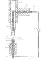
- FIG. 3 is a diagram illustrating a configuration of an atomizer according to the first embodiment.
- 3 is a graph showing the time dependence of the emission intensity by the atomizer of Example 1.
- FIG. 3 is a graph showing the relationship between the pulse width by the atomizer of Example 1 and the temperature of atmospheric pressure plasma.
- 3 is a graph showing the relationship between the pulse width by the atomizer of Example 1 and the electron density of atmospheric pressure plasma.
- 3 is a graph showing the relationship between the pulse width and light emission intensity by the atomizer of Example 1.
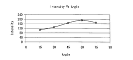
- FIG. 6 is a graph showing the dependence of the emission intensity of atmospheric pressure plasma on the light receiving angle by the atomizer of Example 2.
- FIG. 6 is a graph showing time characteristics of atmospheric pressure plasma emission by the atomizer of Example 2.
- 6 is a graph showing temporal characteristics of Cu emission intensity by the atomizer of Example 2.
- FIG. 1 is a diagram illustrating a configuration of an atomizer according to the first embodiment.
- the atomizer of Example 1 has a rod-shaped electrode 10 (first electrode of the present invention) and a sample electrode 11 (second electrode of the present invention).
- the rod-like electrode 10 is a Cu rod having a diameter of 1.2 mm
- the sample electrode 11 is a stainless steel tube having an outer diameter of 2 m and an inner diameter of 1 mm.
- the outer peripheral surface of the rod-shaped electrode 10 is covered with an insulator 102.
- the rod-like electrode 10 can be made of stainless steel, molybdenum, tungsten, or the like in addition to Cu. In addition to stainless steel, Cu, molybdenum, tungsten, or the like can be used for the sample electrode 11. However, considering that the sample electrode 11 itself is atomized and affects analysis, the sample electrode 11 is made of a material that does not contain the target element, or is coated or plated with a material that does not contain the target element. Etc. need to be applied.
- the tip of the rod-shaped electrode 10 is accommodated in the ceramic tube 12 so that the axial directions thereof coincide.
- the ceramic tube 12 is narrowed by one step on the tip side facing the sample electrode 11, and the rod-shaped electrode 10 extends to the narrowed tube 121.
- a gap 101 is provided between the rod-shaped electrode 10 and the inner wall of the ceramic tube 12.
- a space 101 around the axis of the rod-shaped electrode 10 serves as an Ar gas flow path.
- the ceramic tube 12 is connected to the insulating tube 13.
- the insulating tube 13 has a branch 13 a in a direction perpendicular to the axial direction, and the rod-like electrode 10 extending from the inside 120 of the ceramic tube 12 to the inside 130 of the insulating tube 13 is bent to be inside the branch 13 a of the insulating tube 13. Is inserted and exposed to the outside.
- An insulating material such as a fluororesin can be used for the insulating tube 13.
- a short ceramic tube 14 whose outer diameter is substantially the same as the inner diameter of the ceramic tube 12 is fitted on the tip of the ceramic tube 12 facing the sample electrode 11.
- the insulating tube 13 is connected to a gas cylinder (not shown) filled with Ar as a discharge gas via a pressure reduction / flow rate controller or the like.
- Ar gas supplied from the gas cylinder is supplied in the axial direction from the inside 130 of the insulating tube 13 to the inside 120 of the ceramic tube 12, and a gap 101 between the rod-shaped electrode 10 and the inner wall of the ceramic tube 12 is formed in the rod-shaped electrode 10.
- Ar gas is discharged from the tip 140 of the ceramic tube 14 in the axial direction of the tip.
- He, Ne, N, air, etc. can be used in addition to Ar.
- the sample electrode 11 is covered with a ceramic tube 15 having an inner diameter of 2 mm and an outer diameter of 3 mm.
- the outer diameter of the tip 150 of the ceramic tube 15 is expanded, and a mortar-shaped recess 16 is formed on the end surface 151 of the ceramic tube 15.
- the sample electrode 11 is exposed on the bottom surface 152 of the recess 16.
- a sample to be atomized is held by the recess 16.
- by making the sample electrode 11 tubular it is possible to supply a liquid sample to the recess 16 of the tip 150 of the ceramic tube 15 through the tube.
- the ceramic tube 15 is further covered with a fluororesin material 17.
- the sample electrode 11 does not need to be tubular shape, and it is good also as a rod shape.
- the rod-shaped electrode 10 and the sample electrode 11 are connected to a high-voltage pulse power source 18, and a rectangular pulse voltage in which positive and negative are alternately reversed is applied.
- a voltage to the rod-shaped electrode 10 and the sample electrode 11 while flowing Ar gas in the tube 120 between the rod-shaped electrode 10 and the inner wall of the ceramic tube 12 in the axial direction, the rod-shaped electrode 10 Atmospheric pressure plasma is generated at the tip 11 of the sample, and the atmospheric pressure plasma extends to the sample electrode 11. Then, the atmospheric pressure plasma is irradiated onto the sample held in the recess 16 and the sample is atomized.
- Part of the atomized sample emits light when mixed in atmospheric pressure plasma, and this light emission is received by a light receiving device, and the emission spectrum is analyzed to perform quantitative analysis of the target element in the sample. it can. Further, it is possible to perform an absorption analysis by using a light source that emits a resonance line spectrum of the target element and irradiating the atomized sample with light from the light source.
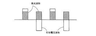
- FIG. 2 is a graph showing the correspondence between the output voltage waveform of the high-voltage pulse power supply 18 and the emission waveform of atmospheric pressure plasma by the atomizer of Example 1.
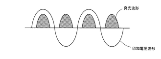
- FIG. 3 is a graph showing a voltage waveform of a conventional commercial AC power supply and an emission waveform of atmospheric pressure plasma by an atomizer of a comparative example.
- the atomizer of the comparative example is an atomizer that boosts the voltage of the commercial AC power supply in place of the pulse high voltage power supply in the atomizer of the first embodiment.
- FIG. 4 shows an emission analyzer using the atomizer and the light receiving device of Example 1, and using a water containing 1 ppm of Pb as a sample, the resonance line spectrum of Pb in the sample (wavelength: 283.3 nm) by the emission analyzer. It is the graph which measured the emitted light intensity of.
- the horizontal axis is the elapsed time after applying the voltage.
- the high-voltage pulse power supply 18 a power supply having a duty ratio of 20% at 100 Hz and a power supply having a duty ratio of 30% at 150 Hz were used. In both cases, the pulse width is 2 ms, and the pulse interval is different.
- the emission intensity is very weak even at the peak.
- the high-voltage pulse power supply 18 when the high-voltage pulse power supply 18 was used, the emission intensity at the peak was stronger than when the commercial AC power supply was used.
- the peak of the emission intensity at 150 Hz with a duty ratio of 30% was about 5 times stronger than that with a commercial AC power supply, and about 2.5 times stronger than at 100 Hz with a duty ratio of 20%.
- FIG. 5 is a graph showing the relationship between the pulse width of the output voltage of the high-voltage pulse power supply 18 and the temperature of the atmospheric pressure plasma.
- the sample water containing 1 ppm of Cu was used.
- the plasma temperature Tg gradually rises until the pulse width is around 2 ms, but when it exceeds 2 ms, the plasma temperature is almost constant.
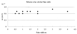
- FIG. 6 is a graph showing the relationship between the pulse width of the output voltage of the high-voltage pulse power supply 18 and the electron density ne of the atmospheric pressure plasma. As can be seen from FIG. 6, the electron density ne does not depend much on the pulse width and is a substantially constant value.
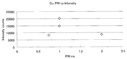
- FIG. 7 is a graph showing the relationship between the pulse width of the output voltage of the high-voltage pulse power supply 18 and the light emission intensity. This is the emission intensity of the resonance line spectrum (wavelength 324 nm) of Cu in a sample using water containing 1 ppm of Cu as a sample. As shown in FIG. 7, the emission intensity depends on the pulse width, and it can be seen that a peak of the emission intensity exists when the pulse width is about 1 ms.
- the emission intensity depends on the pulse width and pulse interval of the output voltage of the high-voltage pulse power supply 18, and the emission intensity (atomization efficiency of the sample) is controlled by controlling the pulse width and pulse interval. I found it possible.
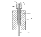
- FIG. 8 is a diagram illustrating the configuration of the atomizer of the second embodiment.
- the atomizer of Example 2 has a rod-shaped electrode 10 (first electrode of the present invention) and a sample electrode 11 (second electrode of the present invention).
- the rod-like electrode 10 is a Cu rod having a diameter of 1.2 mm
- the sample electrode 11 is a stainless steel tube having an outer diameter of 2 m and an inner diameter of 1 mm.
- the rod-like electrode 10 can be made of stainless steel, molybdenum, tungsten, or the like in addition to Cu. In addition to stainless steel, Cu, molybdenum, tungsten, or the like can be used for the sample electrode 11. However, considering that the sample electrode 11 itself is atomized and affects analysis, the sample electrode 11 is made of a material that does not contain the target element, or is coated or plated with a material that does not contain the target element. Etc. need to be applied.
- FIG. 9 is an enlarged view showing the configuration of the rod-shaped electrode 10 portion of the atomizer.
- the outer peripheral surface of the rod-shaped electrode 10 is covered with an insulator 102.
- the distal end portion 111 of the rod-shaped electrode 10 is accommodated in the tube 120 of the ceramic tube 12 so that the axial directions thereof coincide with each other.
- the tip 122 facing the sample electrode 11 is narrowed by one step, and the rod-shaped electrode 10 extends to the position of the narrowed tip 122.
- a gap 101 is provided between the rod-shaped electrode 10 and the inner wall of the ceramic tube 12.
- a space around the axis of the rod-shaped electrode 10 becomes a flow path of Ar gas.
- the ceramic tube 12 is connected to the insulating tube 13 at the root.
- the insulating tube 13 has a branch 13 a in a direction perpendicular to the axial direction, and the rod-like electrode 10 extending from the inside 120 of the ceramic tube 12 to the inside 130 of the insulating tube 13 is bent to be inside the branch 13 a of the insulating tube 13. Is inserted and exposed to the outside.
- An insulating material such as a fluororesin can be used for the insulating tube 13.
- a short ceramic tube 14 having an outer diameter substantially coincident with the inner diameter of the ceramic tube 12 is fitted into the tip 122 of the ceramic tube 12 facing the sample electrode 11.
- the insulating tube 13 is connected to a gas cylinder (not shown) filled with Ar as a discharge gas via a pressure reduction / flow rate controller or the like.
- Ar gas supplied from the gas cylinder is supplied in the axial direction from the inside of the insulating tube 13 to the inside 120 of the ceramic tube 12, and a gap 101 between the rod-shaped electrode 10 and the inner wall of the ceramic tube 12 is disposed on the tip side of the rod-shaped electrode 10.
- Ar gas is discharged from the tip 140 of the ceramic tube 14 in the axial direction.
- He, Ne, N, air, etc. can be used in addition to Ar.
- FIG. 10 is an enlarged view showing the configuration of the sample electrode 11 portion of the atomizer.
- the sample electrode 11 is covered with a ceramic tube 15 having an inner diameter of 2 mm and an outer diameter of 3 mm.
- the outer diameter of the tip 150 of the ceramic tube 15 is expanded, and a mortar-shaped recess 16 is formed on the end surface 151 of the ceramic tube 15.
- the sample electrode 11 is exposed on the bottom surface 152 of the recess 16.
- a sample to be atomized is held by the recess 16.
- the ceramic tube 15 is further covered with a fluororesin material 17.
- the sample electrode 11 does not need to be tubular, and it is good also as a rod shape.
- the rod-shaped electrode 10 and the sample electrode 11 are connected to a 60 Hz AC power source 18 and applied with a voltage.
- a voltage By applying a voltage to the rod-shaped electrode 10 and the sample electrode 11 while flowing Ar gas in the gap 101 between the rod-shaped electrode 10 and the inner wall of the ceramic tube 12 in the axial direction on the distal end side of the rod-shaped electrode 10, Atmospheric pressure plasma is generated at the tip 111, and the atmospheric pressure plasma extends to the sample electrode 11. Then, the atmospheric pressure plasma is irradiated onto the sample held in the recess 16 and the sample is atomized.
- Part of the atomized sample emits light when mixed in atmospheric pressure plasma, and this light emission is received by a light receiving device, and the emission spectrum is analyzed to perform quantitative analysis of the target element in the sample. it can. Further, it is possible to perform an absorption analysis by using a light source that emits a resonance line spectrum of the target element and irradiating the atomized sample with light from the light source.
- the atomizer of the second embodiment described above is not a structure using two power sources like the conventional atomizer using atmospheric pressure plasma, but a structure using a single power source, so that the apparatus can be miniaturized. Yes, a portable atomizer can be realized.
- FIG. 11 is a graph showing the results of measuring the light-receiving angle dependence of the emission intensity of atmospheric pressure plasma obtained by the atomizer of Example 2.
- the horizontal axis indicates the light receiving angle, and the light receiving angle is an angle formed by a straight line connecting the sample and the light receiving device with a plane perpendicular to the opposing direction (axial direction) of the rod electrode 10 and the sample electrode 11.
- the light receiving device is an optical fiber having a lens at an end, and the optical fiber is connected to the spectroscopic device.
- the sample was water containing 1 ppm of Cu, and the light emission intensity at a resonance line spectrum wavelength (324.75 nm) of Cu was measured by a light receiving device.
- the distance between the rod-shaped electrode 10 and the sample electrode 11 was 4 mm, and the distance from the sample to the light receiving device was 4 mm.
- the detected light intensity was high when the light receiving angle was 45 to 75 °, and the highest detected light intensity was when the light receiving angle was 60 °.
- the distance dependency between the sample and the light receiving device was measured.
- the light receiving angle was 60 °, and other conditions were the same as those in FIG.
- the detected emission intensity has a measurement distance dependency, and the detected emission intensity at 36 mm was the highest.
- the measurement distance is considered to have wavelength dependence, it is considered that there is an optimum measurement distance in the case of the resonance line spectrum of other elements as in the case of Cu.
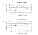
- FIG. 13 is a graph showing the results of measuring the Ar gas flow rate dependency of the emission intensity of atmospheric pressure plasma.
- the distance between the rod-shaped electrode 10 and the sample electrode 11 was 6 mm.
- water containing 1 ppm of Cu and water containing 20 ppm of Cu were prepared as samples.
- FIG. 13A shows the case of water containing 1 ppm of Cu
- FIG. 13B shows the case of water containing 20 ppm of Cu.
- the emission intensity was maximum at 0.4 L / min. This is presumably because when the flow rate is low, the plasma becomes unstable and the emission intensity decreases, and when the flow rate is high, the atomized sample scatters and the emission intensity decreases.
- the Ar gas flow rate is preferably 0.2 liter / min or more and 0.8 liter / min or less.
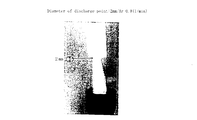
- FIG. 14 is a photograph showing atmospheric pressure plasma when the inner diameter of the ceramic tube 14 is 2 mm
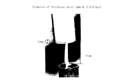
- FIG. 15 is a photograph showing atmospheric pressure plasma when the inner diameter is 3 mm.
- the inner diameter of the ceramic tube 14 is increased, the atmospheric pressure plasma becomes thicker, and it is expected that the plasma irradiation range to the sample can be expanded and the emission intensity can be improved, but as can be seen by comparing FIGS. Even if the inner diameter was changed from 2 mm to 3 mm, the atmospheric pressure plasma did not increase. Further, when the inner diameter was 3 mm, the plasma became unstable and did not have a uniform thickness. As a result, the inner diameter of the ceramic tube 14 is desirably 2 mm or less.
- the optimum value of the inner diameter depends on components such as the power source capacity, the material of the rod-shaped electrode 10 and the diameter.
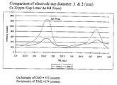
- FIG. 16 is a diagram showing an emission spectrum when the diameter of the recess 16 is 2 mm and 3 mm. As shown in FIG. 16, it was found that the larger the diameter of the concave portion 16 holding the sample, the higher the emission intensity. From this result, it was found that there is an optimum value for maximizing the emission intensity in the diameter of the recess 16. It is desirable that the diameter of the recess 16 be 3 mm or more.
- the sample injection method is a method of supplying a constant amount of a liquid sample through the tube of the sample electrode 11 to the concave portion 16 as needed.
- the quantitative supply method is a method of supplying a certain amount of liquid sample to the recess 16 for each measurement. As a result of examining these two methods through experiments, it has been found that the quantitative supply method is preferable in terms of reproducibility and stability during measurement.
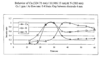
- FIG. 17 is a graph showing temporal characteristics of light emission intensities of Cu, H, and N.
- Cu has a wavelength of 324.75 nm
- H has a wavelength of 486.13 nm
- N has a wavelength of 380 nm.
- the time axis is based on the time when the atomized plasma was ignited. As shown in FIG. 17, the peak of hydrogen emission intensity and the peak of copper emission intensity almost coincide.
- FIG. 18 is a graph showing the results. As a result, it was found that the reproducibility of the peak of Cu emission intensity was about 10%.
- Example 7 Using the sewage sample as a sample, the effectiveness of the emission analyzer using the atomizer of Example 1 was confirmed.
- the concentrations of Cu and Zn in the sewage sample were measured in advance by an emission analysis using an ICP device, and found to be 3.5 ppm and 10 ppm, respectively.
- FIG. 19A shows the result of measuring the concentration of Cu
- FIG. 19B shows the result of measuring the concentration of Zn.
- the rhombus plots are the results of measurement for standard samples with known concentrations (Cu concentrations or Zn concentrations of 0.5 ppm, 1 ppm, and 2 ppm, respectively). Further, in FIG.
- black circle plots indicate the concentrations of Cu and Zn in the sewage sample measured by the ICP apparatus.
- the rhombus plot showing the measurement results of the Cu and Zn concentrations in the sewage sample by the emission spectrometer using the atomizer of Example 1 overlaps the black circle plot in the figure. As a result, it was confirmed that the emission analyzer using the atomizer of Example 1 was capable of quantitative analysis with high accuracy.
- the atomizer of the present invention can be used in analyzers such as absorption analysis and luminescence analysis.
- Rod electrode 11 Sample electrode 12, 14, 15: Ceramic tube 13: Insulating tube 16: Recessed portion 17: Fluorine resin material 18: Power supply
Landscapes
- Physics & Mathematics (AREA)
- Engineering & Computer Science (AREA)
- Plasma & Fusion (AREA)
- Spectroscopy & Molecular Physics (AREA)
- Health & Medical Sciences (AREA)
- Life Sciences & Earth Sciences (AREA)
- Analytical Chemistry (AREA)
- Geology (AREA)
- General Life Sciences & Earth Sciences (AREA)
- Nuclear Medicine, Radiotherapy & Molecular Imaging (AREA)
- Chemical & Material Sciences (AREA)
- Environmental & Geological Engineering (AREA)
- Biochemistry (AREA)
- General Health & Medical Sciences (AREA)
- General Physics & Mathematics (AREA)
- Immunology (AREA)
- Pathology (AREA)
- Investigating, Analyzing Materials By Fluorescence Or Luminescence (AREA)
- Plasma Technology (AREA)
Abstract
【課題】アトマイゼーションの高効率化を図ること。 【解決手段】アトマイザーは、棒状電極10と、棒状電極10の先端部から一定距離隔てて配置された試料電極11を有している。棒状電極10の先端部は、軸方向を一致させてセラミックス管14内に納められている。セラミックス管14の内壁と棒状電極10との間には隙間が設けられていて、放電ガスがこの隙間を棒状電極10の先端側軸方向に流される。試料電極11は、セラミックス管15によって覆われていて、セラミックス管15の先端は外径が拡張されており、すり鉢状の凹部16を有している。凹部16底面には、試料電極11が露出している。この凹部に試料を保持する。棒状電極10、試料電極11は高圧パルス電源18に接続されている。高圧パルス電源18は、図2のように、正負が交互に反転する矩形パルス電圧を出力する。
Description
本発明は、大気圧プラズマを用いて試料中の目的とする元素の原子化を行うアトマイザーに関するものであり、大気圧プラズマを発生させるための電源に特徴を有するものである。また、本発明は、そのアトマイザーを用いた発光分析装置に関するものである。
原子吸光分析や原子発光分析では、試料を原子化する装置(アトマイザー)が必要となるが、従来よりアトマイザーとして原子吸光分析では黒鉛炉、原子発光分析ではICP装置などが広く用いられている。また、特許文献1のように、大気圧プラズマを用いたアトマイザーも知られている。
特許文献1には、以下のような発光分析方法が記載されている。まず、アトマイザーを用いて目的元素を含む試料に大気圧プラズマを照射して試料を原子化し、その原子化された試料中の金属元素蒸気を大気圧プラズマ中に混入させ、プラズマ中の高エネルギー電子によって励起発光させる。この発光を分光器を通して測定し、試料中の目的元素の密度などを計測する。
すなわち、特許文献1に記載のアトマイザーは、大気圧プラズマを発生させるプラズマ発生装置と、大気圧プラズマを試料に導き照射する誘導電極とを有しており、プラズマ発生装置の電源と、プラズマ発生装置の電極と誘導電極との間に電圧を印加する電源との2つの電源を備えている。大気圧プラズマはプラズマ温度が低く、電子密度が高いため、効率的に試料を原子化することができる。
すなわち、特許文献1に記載のアトマイザーは、大気圧プラズマを発生させるプラズマ発生装置と、大気圧プラズマを試料に導き照射する誘導電極とを有しており、プラズマ発生装置の電源と、プラズマ発生装置の電極と誘導電極との間に電圧を印加する電源との2つの電源を備えている。大気圧プラズマはプラズマ温度が低く、電子密度が高いため、効率的に試料を原子化することができる。
また、上記アトマイザーの大気圧プラズマの発生には、商用のAC電源の電圧を昇圧して電極に印加することが記載されている。
しかし、商用AC電源を用いた場合、電圧がなだらかに上昇するため放電開始電圧になるまでに時間遅れが生じ、原子化の効率が悪かった。そのため、目的元素の種類によっては発光強度が低下し、測定が困難であった。
また、特許文献1のアトマイザーは、2つの電源を備えているため、装置を小型化して携帯型とすることができなかった。
また、特許文献1のアトマイザーは、2つの電源を備えているため、装置を小型化して携帯型とすることができなかった。
そこで本発明の目的は、大気圧プラズマを用いたアトマイザーにおいて、原子化の高効率化を図ることである。
また、本発明の他の目的は、大気圧プラズマを用いたアトマイザーの小型化を図ることである。
また、本発明の他の目的は、大気圧プラズマを用いたアトマイザーの小型化を図ることである。
第1の発明は、電源を用いて電圧を印加して大気圧プラズマを発生させ、試料に大気圧プラズマを照射して試料を原子化するアトマイザーであって、電源は、正負が交互に反転する矩形パルス電圧を出力する、ことを特徴とするアトマイザーである。
第2の発明は、第1の発明において、棒状の第1電極と、管状であって、その管内に、第1電極の軸回りにおいて管内壁から第1電極が離間した状態となるように第1電極の先端部を保持し、管内壁と第1電極との隙間に、第1電極の先端部側の軸方向に放電ガスが流される絶縁管と、第1電極の先端部から一定距離隔てて配置された第2電極と、試料を保持する凹部を有し、その凹部底面に第2電極が露出した絶縁材からなる試料保持部と、を有し、電源は、第1電極および前記第2電極間に電圧を印加する、ことを特徴とするアトマイザーである。
第3の発明は、棒状の第1電極と、管状であって、その管内に、第1電極の軸回りにおいて管内壁から第1電極が離間した状態となるように第1電極の先端部を保持し、管内壁と第1電極との隙間に、第1電極の先端部側の軸方向に放電ガスが流される絶縁管と、第1電極の先端部から一定距離隔てて配置された第2電極と、試料を保持する凹部を有し、その凹部底面に第2電極が露出した絶縁材からなる試料保持部と、第1電極および第2電極間に電圧を印加する交流電源と、を有することを特徴とするアトマイザーである。
放電ガスには、Ar、He、窒素、酸素、空気などを用いることができる。
第1電極および第2電極の材料は、SUS、銅、タングステンなどを用いることができる。ただし、第2電極には、分析の目標となる元素を含む材料を用いないようにするか、もしくは分析の目標となる元素を含まない材料によって被膜、めっき等を施す必要がある。第2電極が原子化されて分析に影響を与えてしまうのを避けるためである。
第4の発明は、第3の発明のアトマイザーと、試料を中心として、第1電極と第2電極との対向方向に垂直な面に対して45~75°の角度で、アトマイザーによって原子化された試料を含む大気圧プラズマの発光を受光して分光分析する分光装置と、を備えた発光分析装置である。
受光角度をこのような範囲とすることで、分析に十分な発光強度を得ることができる。より望ましい角度は、60°である。
本第1、第2の発明によれば、矩形波の立ち上がり、立ち下がりの鋭さから、瞬時に放電開始電圧まで印加することができ、発光強度の高い状態が一定期間保たれるため、試料の原子化の高効率化を図ることができる。その結果、発光強度が向上し、分析精度の向上を図ることができる。また、電圧をパルス化することでプラズマ温度の上昇を抑制し、原子化した試料の分散が抑えられる。その結果、原子化した試料の密度が向上し、大気圧プラズマに含まれる原子化された試料の密度も向上し、発光強度が向上する。また、正の矩形パルスと負の矩形パルスを交互に印加するため、大気圧プラズマを安定に生成することができる。
第3の発明のアトマイザーは、電源が1つであるため小型化が可能であり、これにより携帯型のアトマイザーを実現することができる。
また、第4の発明の発光分析装置によると、分析に十分な発光強度を得ることができるので、分析の精度を向上させることができる。
以下、本発明の具体的な実施例について、図を参照に説明するが、本発明は実施例に限定されるものではない。
図1は、実施例1のアトマイザーの構成を示した図である。実施例1のアトマイザーは、棒状電極10(本発明の第1電極)と、試料電極11(本発明の第2電極)とを有している。棒状電極10は、直径1.2mmのCu製の棒状であり、試料電極11は、外径2m、内径1mmのステンレス製の管状である。棒状電極10の外周面は絶縁体102により被覆されている。
棒状電極10には、Cu以外に、ステンレス、モリブデン、タングステンなどを用いることができる。また、試料電極11には、ステンレス以外に、Cu、モリブデン、タングステンなどを用いることができる。ただし、試料電極11自体が原子化してしまい、分析に影響を与えてしまうことを考慮して、試料電極11には目的元素を含まない材料を用いるか、目的元素を含まない材料で被膜、めっき等を施す必要がある。
棒状電極10の先端部は、セラミックス管12の管内に軸方向を一致させて納められている。セラミックス管12は、試料電極11に対向する先端側が一段階狭くなっていて、棒状電極10は、この狭くなった管内121まで伸びている。棒状電極10とセラミックス管12の内壁との間には隙間101が設けられている。この棒状電極10の軸回りの空間101がArガスの流路となる。
セラミックス管12は、絶縁管13と連結している。絶縁管13は軸方向に垂直な方向に分岐13aを有しており、セラミックス管12の管内120から絶縁管13の管内130に伸びる棒状電極10は、曲げられて絶縁管13の分岐13aの管内に挿入され、外部に露出している。絶縁管13には、フッ素樹脂などの絶縁材を用いることができる。
さらに、セラミックス管12の試料電極11に対向する先端部側には、外径がセラミックス管12の内径にほぼ一致した短いセラミックス管14がはめ込まれている。
絶縁管13は放電用ガスであるArが封入されたガスボンベ(図示しない)に、減圧・流量制御器などを介して接続されている。ガスボンベから供給されたArガスは、絶縁管13の管内130からセラミックス管12の管内120へと軸方向に供給され、棒状電極10とセラミックス管12の内壁との間の隙間101を棒状電極10の先端部の軸方向に流れてセラミックス管14の先端140からArガスが排出される。
放電ガスには、Ar以外にもHe、Ne、N、空気、などを用いることができる。
試料電極11は、内径2mm、外径3mmのセラミックス管15によって覆われている。セラミックス管15の先端150は外径が拡張されており、セラミックス管15の端面151にはすり鉢状の凹部16が形成されている。凹部16の底面152には、試料電極11が露出している。この凹部16によって、原子化する試料を保持する。また、試料電極11を管状とすることで、その管内を通してセラミックス管15の先端150の凹部16に液体の試料を供給することが可能となっている。また、セラミックス管15はフッ素樹脂材17によってさらに覆われている。なお、凹部16に一定量の試料を保持する場合には、試料電極11を管状とする必要はなく、棒状などとしてもよい。
棒状電極10、試料電極11は高圧パルス電源18に接続されており、正負が交互に反転する矩形パルス電圧が印加される。Arガスを棒状電極10とセラミックス管12の内壁との間の管内120に棒状電極10の先端部の軸方向に流しながら、棒状電極10、試料電極11に電圧を印加することで、棒状電極10の先端部11に大気圧プラズマが生じ、その大気圧プラズマが試料電極11に伸びていく。そして、大気圧プラズマが凹部16に保持された試料に照射され、試料が原子化される。原子化された試料の一部は、大気圧プラズマに混入して発光し、この発光を受光装置によって受光して発光スペクトルを解析することで、試料中の目的元素の定量分析などを行うことができる。また、目的元素の共鳴線スペクトルを発光する光源を用い、その光源の光を原子化された試料に照射して吸光分析を行うこともできる。
図2は、高圧パルス電源18の出力電圧波形と、実施例1のアトマイザーによる大気圧プラズマの発光波形との対応を示したグラフである。また、図3は、従来の商用AC電源の電圧波形と、比較例のアトマイザーによる大気圧プラズマの発光波形とを示したグラフである。ここで比較例のアトマイザーとは、実施例1のアトマイザーにおいて、パルス高圧電源に替えて商用AC電源の電圧を昇圧して用いたアトマイザーである。
図3のように、商用AC電源を用いた場合は、電圧がなだらかに上昇するために放電開始電圧になるまでに時間遅れが生じ、また大気圧プラズマの発光強度も徐々に増加、減少する状態となっている。すなわち、商用AC電源を用いた場合には試料の原子化の効率が低下してしまう。
一方、図2のように正負が交互に反転する矩形パルス電圧を用いる場合には、出力電圧が瞬時に放電開始電圧まで上昇するため、大気圧プラズマの発光強度も瞬時に上昇し、発光強度はパルス高圧電源のパルス幅とほぼ同様の期間、発光強度の高い状態で一定に維持される。そのため、試料の原子化を高効率に行うことができる。また、電圧がパルスであるため、プラズマ温度の上昇が抑制され、原子化された試料の発散が抑制される。そのため、原子化された試料の密度が向上し、大気圧プラズマに含まれる原子化された試料の密度も向上する。その結果、試料中の目的元素の発光強度を向上させることができる。また、正負が交互に反転するパルスであるため、大気圧プラズマを安定して生成することができる。
図4は、実施例1のアトマイザーと受光装置とを用いて発光分析装置を構成し、1ppmのPbを含む水を試料として、発光分析装置によって試料中のPbの共鳴線スペクトル(波長283.3nm)の発光強度を測定したグラフである。横軸は電圧を印加後の経過時間である。高圧パルス電源18は、100Hzでデューティ比が20%の電源と、150Hzでデューティ比が30%の電源を用いた。ともにパルス幅は2msであり、パルス間隔が異なっている。また、実施例1のアトマイザーに替えて、商用AC電源を用いる比較例のアトマイザーを用いた場合のPbの共鳴線スペクトルの発光強度も測定した。
図4のように、商用AC電源を用いた場合は、発光強度がピークにおいても非常に弱い。一方、高圧パルス電源18を用いた場合は、ピークにおける発光強度が商用AC電源を用いた場合に比べて強かった。特に150Hzでデューティ比30%の場合の発光強度のピークは、商用AC電源の場合よりも約5倍強く、100Hzでデューティ比が20%の場合よりも約2.5倍強かった。
図5は、高圧パルス電源18の出力電圧のパルス幅と大気圧プラズマの温度の関係を示したグラフである。試料には1ppmのCuを含む水を用いた。図5のように、パルス幅が2msあたりまではプラズマ温度Tgはゆるやかに上昇するが、2msを越えると、プラズマ温度はほぼ一定となっていることがわかる。
図6は、高圧パルス電源18の出力電圧のパルス幅と大気圧プラズマの電子密度neとの関係を示したグラフである。図6のように、電子密度neはパルス幅にあまり依存せず、ほぼ一定の値であることがわかる。
図7は、高圧パルス電源18の出力電圧のパルス幅と発光強度との関係を示したグラフである。1ppmのCuを含む水を試料とし、試料中のCuの共鳴線スペクトル(波長324nm)の発光強度である。図7のように、発光強度はパルス幅に依存しており、パルス幅が1msぐらいの場合に発光強度のピークが存在していることがわかる。
図4および図7の結果から、発光強度は高圧パルス電源18の出力電圧のパルス幅、パルス間隔に依存しており、パルス幅、パルス間隔の制御によって発光強度(試料の原子化効率)を制御可能であることがわかった。
次に、実施例2について説明する。図8は、実施例2のアトマイザーの構成を示した図である。実施例2のアトマイザーは、棒状電極10(本発明の第1電極)と、試料電極11(本発明の第2電極)とを有している。棒状電極10は、直径1.2mmのCu製の棒状であり、試料電極11は、外径2m、内径1mmのステンレス製の管状である。
棒状電極10には、Cu以外に、ステンレス、モリブデン、タングステンなどを用いることができる。また、試料電極11には、ステンレス以外に、Cu、モリブデン、タングステンなどを用いることができる。ただし、試料電極11自体が原子化してしまい、分析に影響を与えてしまうことを考慮して、試料電極11には目的元素を含まない材料を用いるか、目的元素を含まない材料で被膜、めっき等を施す必要がある。
図9は、アトマイザーの棒状電極10部分の構成を拡大して示した図である。棒状電極10の外周面は絶縁体102により被覆されている。棒状電極10の先端部111は、セラミックス管12の管内120に軸方向を一致させて納められている。セラミックス管12は、試料電極11に対向する先端部122が一段階狭くなっていて、棒状電極10は、この狭くなった先端部122の位置まで伸びている。棒状電極10とセラミックス管12の内壁との間には隙間101が設けられている。この棒状電極10の軸回りの空間がArガスの流路となる。
セラミックス管12は、根元において絶縁管13と連結している。絶縁管13は軸方向に垂直な方向に分岐13aを有しており、セラミックス管12の管内120から絶縁管13の管内130に伸びる棒状電極10は、曲げられて絶縁管13の分岐13aの管内に挿入され、外部に露出している。絶縁管13には、フッ素樹脂などの絶縁材を用いることができる。
さらに、セラミックス管12の試料電極11に対向する先端部122には、外径がセラミックス管12の内径にほぼ一致した短いセラミックス管14がはめ込まれている。
絶縁管13は放電用ガスであるArが封入されたガスボンベ(図示しない)に、減圧・流量制御器などを介して接続されている。ガスボンベから供給されたArガスは、絶縁管13の管内からセラミックス管12の管内120へと軸方向に供給され、棒状電極10とセラミックス管12の内壁との隙間101を棒状電極10先端部側の軸方向に流れてセラミックス管14の先端140からArガスが排出される。
放電ガスには、Ar以外にもHe、Ne、N、空気、などを用いることができる。
図10は、アトマイザーの試料電極11部分の構成を拡大して示した図である。試料電極11は、内径2mm、外径3mmのセラミックス管15によって覆われている。セラミックス管15の先端150は外径が拡張されており、セラミックス管15の端面151にはすり鉢状の凹部16が形成されている。凹部16の底面152には、試料電極11が露出している。この凹部16によって、原子化する試料を保持する。また、試料電極11を管状とすることで、その管内を通してセラミックス管15の先端150の凹部16に液体の試料を供給することが可能となっている。また、セラミックス管15はフッ素樹脂材17によってさらに覆われている。なお、凹部に一定量の試料を保持する場合には、試料電極11を管状とする必要はなく、棒状などとしてもよい。
棒状電極10、試料電極11は60Hzの交流電源18に接続されており、電圧が印加される。Arガスを棒状電極10とセラミックス管12の内壁との隙間101に棒状電極10の先端部側の軸方向に流しながら、棒状電極10、試料電極11に電圧を印加することで、棒状電極10の先端部111に大気圧プラズマが生じ、その大気圧プラズマが試料電極11に伸びていく。そして、大気圧プラズマが凹部16に保持された試料に照射され、試料が原子化される。原子化された試料の一部は、大気圧プラズマに混入して発光し、この発光を受光装置によって受光して発光スペクトルを解析することで、試料中の目的元素の定量分析などを行うことができる。また、目的元素の共鳴線スペクトルを発光する光源を用い、その光源の光を原子化された試料に照射して吸光分析を行うこともできる。
以上に説明した実施例2のアトマイザーは、従来の大気圧プラズマを用いたアトマイザーのような2つの電源を用いる構造ではなく、単一の電源を用いる構造であるから、装置の小型化が可能であり、携帯型アトマイザーを実現することができる。
次に、実施例2のアトマイザーを用いた各種実験結果について説明する。
[実験例1]
図11は、実施例2のアトマイザーによって得られる大気圧プラズマの発光強度の受光角度依存性を測定した結果を示すグラフである。横軸は、受光角度を示しており、受光角度は、試料と受光装置とを結ぶ直線が、棒状電極10と試料電極11との対向方向(軸方向)に垂直な面と成す角度である。受光装置は、端部にレンズが設けられた光ファイバーであり、光ファイバーは分光装置に接続されている。試料は1ppmのCuを含む水とし、Cuの共鳴線スペクトル波長(324.75nm)での発光強度を受光装置により測定した。また、棒状電極10と試料電極11との距離は4mmとし、試料から受光装置までの距離は4mmとした。図11のように、受光角度を45~75°としたときに検出される発光強度が高く、最も検出される発光強度が高かったのは受光角度が60°の時であった。
図11は、実施例2のアトマイザーによって得られる大気圧プラズマの発光強度の受光角度依存性を測定した結果を示すグラフである。横軸は、受光角度を示しており、受光角度は、試料と受光装置とを結ぶ直線が、棒状電極10と試料電極11との対向方向(軸方向)に垂直な面と成す角度である。受光装置は、端部にレンズが設けられた光ファイバーであり、光ファイバーは分光装置に接続されている。試料は1ppmのCuを含む水とし、Cuの共鳴線スペクトル波長(324.75nm)での発光強度を受光装置により測定した。また、棒状電極10と試料電極11との距離は4mmとし、試料から受光装置までの距離は4mmとした。図11のように、受光角度を45~75°としたときに検出される発光強度が高く、最も検出される発光強度が高かったのは受光角度が60°の時であった。
また、試料と受光装置との間の距離依存性についても測定した。受光角度は60°とし、他の条件は図11の場合と同一とした。図12に示すように、検出される発光強度には測定距離依存性があり、36mmで検出される発光強度が最も高かった。測定距離には波長依存性があると考えられるが、他の元素の共鳴線スペクトルの場合にも、Cuの場合と同様に、最適な測定距離が存在するものと考えられる。
[実験例2]
図13は、大気圧プラズマの発光強度のArガス流量依存性を測定した結果を示すグラフである。棒状電極10と試料電極11との距離は6mmとした。また、試料として1ppmのCu含む水と、20ppmのCuを含む水を用意した。図13(a)が1ppmのCu含む水の場合、図13(b)が20ppmのCuを含む水の場合である。いずれの試料の場合も、0.4L/minで発光強度が最大であった。これは、流量が遅いとプラズマが不安定となって発光強度が低下し、流量が速いと原子化した試料が飛散してしまい発光強度が低下してしまうためと考えられる。このように、Arガス流量の最適値が存在していることがわかった。また、Arガス流量は、0.2 liter/min以上、0.8 liter/min以下が望ましい。
図13は、大気圧プラズマの発光強度のArガス流量依存性を測定した結果を示すグラフである。棒状電極10と試料電極11との距離は6mmとした。また、試料として1ppmのCu含む水と、20ppmのCuを含む水を用意した。図13(a)が1ppmのCu含む水の場合、図13(b)が20ppmのCuを含む水の場合である。いずれの試料の場合も、0.4L/minで発光強度が最大であった。これは、流量が遅いとプラズマが不安定となって発光強度が低下し、流量が速いと原子化した試料が飛散してしまい発光強度が低下してしまうためと考えられる。このように、Arガス流量の最適値が存在していることがわかった。また、Arガス流量は、0.2 liter/min以上、0.8 liter/min以下が望ましい。
[実験例3]
図14はセラミックス管14の内径を2mmとした場合の大気圧プラズマを示した写真、図15は内径を3mmとした場合の大気圧プラズマを示した写真である。セラミックス管14の内径を大きくすると大気圧プラズマが太くなり、試料へのプラズマ照射範囲が広がって発光強度を向上することができるのではと期待したが、図14、15を比較するとわかるように、内径を2mmから3mmにしても大気圧プラズマが太くなるわけではなかった。また、内径を3mmとした場合にはプラズマが不安定となり、均一な太さにはならなかった。この結果、セラミックス管14の内径は、2mm以下が望ましい。また、この結果から、太くて安定した大気圧プラズマが得られる内径の最適値が存在していると思われる。また、その内径の最適値は、電源容量や棒状電極10の材料、直径などの構成要素に依存しているものと考えられる。
図14はセラミックス管14の内径を2mmとした場合の大気圧プラズマを示した写真、図15は内径を3mmとした場合の大気圧プラズマを示した写真である。セラミックス管14の内径を大きくすると大気圧プラズマが太くなり、試料へのプラズマ照射範囲が広がって発光強度を向上することができるのではと期待したが、図14、15を比較するとわかるように、内径を2mmから3mmにしても大気圧プラズマが太くなるわけではなかった。また、内径を3mmとした場合にはプラズマが不安定となり、均一な太さにはならなかった。この結果、セラミックス管14の内径は、2mm以下が望ましい。また、この結果から、太くて安定した大気圧プラズマが得られる内径の最適値が存在していると思われる。また、その内径の最適値は、電源容量や棒状電極10の材料、直径などの構成要素に依存しているものと考えられる。
[実験例4]
試料を保持する凹部16の直径の違いによる発光強度を比較した。凹部16の直径は、2、3、4mmとした。棒状電極10から試料電極11までの距離は6mm、Arガス流量は0.8L/min、試料には10ppmのCuを含む水を用いた。4mmでは、試料電極11表面でのプラズマ位置が不安定となった。図16は、凹部16の直径を2mm、3mmとしたときの、発光スペクトルを示した図である。図16のように、試料を保持する凹部16の直径が大きい方が発光強度も向上することがわかった。この結果から、凹部16の直径には発光強度を最大とする最適値が存在していることがわかった。凹部16の直径を3mm以上とすることが望ましい。
試料を保持する凹部16の直径の違いによる発光強度を比較した。凹部16の直径は、2、3、4mmとした。棒状電極10から試料電極11までの距離は6mm、Arガス流量は0.8L/min、試料には10ppmのCuを含む水を用いた。4mmでは、試料電極11表面でのプラズマ位置が不安定となった。図16は、凹部16の直径を2mm、3mmとしたときの、発光スペクトルを示した図である。図16のように、試料を保持する凹部16の直径が大きい方が発光強度も向上することがわかった。この結果から、凹部16の直径には発光強度を最大とする最適値が存在していることがわかった。凹部16の直径を3mm以上とすることが望ましい。
[実験例5]
試料の供給方法の違いについて、サンプル注入法と定量供給法の2つの方法を検討した。サンプル注入法は、試料電極11の管内を通して凹部16に液体試料を随時一定量供給する方法である。定量供給法は、測定毎に凹部16に一定量の液体試料を供給する方法である。この2つの方法を実験により検討した結果、再現性、測定時の安定性などの点から定量供給法が好ましいことがわかった。
試料の供給方法の違いについて、サンプル注入法と定量供給法の2つの方法を検討した。サンプル注入法は、試料電極11の管内を通して凹部16に液体試料を随時一定量供給する方法である。定量供給法は、測定毎に凹部16に一定量の液体試料を供給する方法である。この2つの方法を実験により検討した結果、再現性、測定時の安定性などの点から定量供給法が好ましいことがわかった。
[実験例6]
大気圧プラズマの発光の時間特性を測定した。試料には1ppmのCuを含む水を用い、Arガス流量は0.4L/min、棒状電極10と試料電極11との間隔は4mmとした。図17は、Cu、H、Nの発光強度の時間特性を示したグラフである。Cuは324.75nm、Hは486.13nm、Nは380nmの波長である。時間軸はアトマイズプラズマを点火した時間を原点としている。図17のように、水素の発光強度のピークと、銅の発光強度のピークがほぼ一致している。これは、大気圧プラズマにより試料の水が蒸発して原子化されると同時に、水に含まれるCuも原子化されていることを示している。また、H、Cuの発光強度のピークから遅れてNの発光強度が増加しているが、これは試料が蒸発するにしたがって空気が混入していくためである。また、Cuの発光強度の時間特性について、再現性を確認するために、3回測定を繰り返した。図18はその結果を示したグラフである。この結果、Cuの発光強度のピークの再現性は10%程度であることがわかった。
大気圧プラズマの発光の時間特性を測定した。試料には1ppmのCuを含む水を用い、Arガス流量は0.4L/min、棒状電極10と試料電極11との間隔は4mmとした。図17は、Cu、H、Nの発光強度の時間特性を示したグラフである。Cuは324.75nm、Hは486.13nm、Nは380nmの波長である。時間軸はアトマイズプラズマを点火した時間を原点としている。図17のように、水素の発光強度のピークと、銅の発光強度のピークがほぼ一致している。これは、大気圧プラズマにより試料の水が蒸発して原子化されると同時に、水に含まれるCuも原子化されていることを示している。また、H、Cuの発光強度のピークから遅れてNの発光強度が増加しているが、これは試料が蒸発するにしたがって空気が混入していくためである。また、Cuの発光強度の時間特性について、再現性を確認するために、3回測定を繰り返した。図18はその結果を示したグラフである。この結果、Cuの発光強度のピークの再現性は10%程度であることがわかった。
[実験例7]
下水サンプルを試料として用い、実施例1のアトマイザーを用いた発光分析装置の有効性について確認した。下水サンプル中のCu、Znの濃度について、事前にICP装置を用いた発光分析によって測定したところ、それぞれ3.5ppm、10ppmであった。図19(a)は、Cuの濃度を測定した結果、図19(b)は、Znの濃度を測定した結果である。図中、菱形のプロットは濃度既知(それぞれ0.5ppm、1ppm、2ppmの濃度のCu濃度またはZn濃度)の標準試料について測定した結果である。また、図19中、黒丸プロットはICP装置により測定した下水サンプル中のCu、Znの濃度である。実施例1のアトマイザーを用いた発光分析装置による下水サンプル中のCu、Znの濃度測定結果を示す菱形プロットは、図中の黒丸プロットと重なっている。この結果、実施例1のアトマイザーを用いた発光分析装置は、高い精度で定量分析が可能であることが確認できた。
下水サンプルを試料として用い、実施例1のアトマイザーを用いた発光分析装置の有効性について確認した。下水サンプル中のCu、Znの濃度について、事前にICP装置を用いた発光分析によって測定したところ、それぞれ3.5ppm、10ppmであった。図19(a)は、Cuの濃度を測定した結果、図19(b)は、Znの濃度を測定した結果である。図中、菱形のプロットは濃度既知(それぞれ0.5ppm、1ppm、2ppmの濃度のCu濃度またはZn濃度)の標準試料について測定した結果である。また、図19中、黒丸プロットはICP装置により測定した下水サンプル中のCu、Znの濃度である。実施例1のアトマイザーを用いた発光分析装置による下水サンプル中のCu、Znの濃度測定結果を示す菱形プロットは、図中の黒丸プロットと重なっている。この結果、実施例1のアトマイザーを用いた発光分析装置は、高い精度で定量分析が可能であることが確認できた。
本発明のアトマイザーは、吸光分析や発光分析などの分析装置に用いることができる。
10:棒状電極
11:試料電極
12、14、15:セラミックス管
13:絶縁管
16:凹部
17:フッ素樹脂材
18:電源
11:試料電極
12、14、15:セラミックス管
13:絶縁管
16:凹部
17:フッ素樹脂材
18:電源
Claims (4)
- 電源を用いて電圧を印加して大気圧プラズマを発生させ、試料に前記大気圧プラズマを照射して前記試料を原子化するアトマイザーであって、
前記電源は、正負が交互に反転する矩形パルス電圧を出力する、
ことを特徴とするアトマイザー。 - 棒状の第1電極と、
管状であって、その管内に、前記第1電極の軸回りにおいて管内壁から前記第1電極が離間した状態となるように前記第1電極の先端部を保持し、管内壁と前記第1電極との隙間に、前記第1電極の先端部側の軸方向に放電ガスが流される絶縁管と、
前記第1電極の先端部から一定距離隔てて配置された第2電極と、
試料を保持する凹部を有し、その凹部底面に前記第2電極が露出した絶縁材からなる試料保持部と、
を有し、
前記電源は、前記第1電極および前記第2電極間に電圧を印加する、
ことを特徴とする請求項1に記載のアトマイザー。 - 棒状の第1電極と、
管状であって、その管内に、前記第1電極の軸回りにおいて管内壁から前記第1電極が離間した状態となるように前記第1電極の先端部を保持し、管内壁と前記第1電極との隙間に、前記第1電極の先端部側の軸方向に放電ガスが流される絶縁管と、
前記第1電極の先端部から一定距離隔てて配置された第2電極と、
試料を保持する凹部を有し、その凹部底面に前記第2電極が露出した絶縁材からなる試料保持部と、
前記第1電極および前記第2電極間に電圧を印加する交流電源と、
を有することを特徴とするアトマイザー。 - 請求項3に記載のアトマイザーと、
前記試料を中心として、前記第1電極と前記第2電極との対向方向に垂直な面に対して45~75°の角度で、前記アトマイザーによって原子化された試料を含む大気圧プラズマの発光を受光して分光分析する分光装置と、
を備えた発光分析装置。
Priority Applications (1)
| Application Number | Priority Date | Filing Date | Title |
|---|---|---|---|
| CN201180032590.0A CN103026206B (zh) | 2010-06-30 | 2011-06-29 | 原子化器以及发光分析装置 |
Applications Claiming Priority (4)
| Application Number | Priority Date | Filing Date | Title |
|---|---|---|---|
| JP2010-150333 | 2010-06-30 | ||
| JP2010-150372 | 2010-06-30 | ||
| JP2010150372A JP5467360B2 (ja) | 2010-06-30 | 2010-06-30 | アトマイザーおよび発光分析装置 |
| JP2010150333A JP5527693B2 (ja) | 2010-06-30 | 2010-06-30 | アトマイザー |
Publications (1)
| Publication Number | Publication Date |
|---|---|
| WO2012001968A1 true WO2012001968A1 (ja) | 2012-01-05 |
Family
ID=45401708
Family Applications (1)
| Application Number | Title | Priority Date | Filing Date |
|---|---|---|---|
| PCT/JP2011/003719 Ceased WO2012001968A1 (ja) | 2010-06-30 | 2011-06-29 | アトマイザーおよび発光分析装置 |
Country Status (2)
| Country | Link |
|---|---|
| CN (1) | CN103026206B (ja) |
| WO (1) | WO2012001968A1 (ja) |
Citations (4)
| Publication number | Priority date | Publication date | Assignee | Title |
|---|---|---|---|---|
| JPH08327552A (ja) * | 1995-06-02 | 1996-12-13 | Hitachi Ltd | 原子吸光分析装置 |
| JP2006302625A (ja) * | 2005-04-19 | 2006-11-02 | Matsushita Electric Works Ltd | プラズマ処理装置及びプラズマ処理方法 |
| JP2008241293A (ja) * | 2007-03-26 | 2008-10-09 | Univ Nagoya | 原子分析装置 |
| JP2009289432A (ja) * | 2008-05-27 | 2009-12-10 | Tokyo Institute Of Technology | プラズマ発生装置及びプラズマ生成方法 |
Family Cites Families (3)
| Publication number | Priority date | Publication date | Assignee | Title |
|---|---|---|---|---|
| US6034485A (en) * | 1997-11-05 | 2000-03-07 | Parra; Jorge M. | Low-voltage non-thermionic ballast-free energy-efficient light-producing gas discharge system and method |
| CN201017845Y (zh) * | 2007-03-14 | 2008-02-06 | 万京林 | 差分馈电介质阻挡放电低温等离子体装置 |
| CN101281135A (zh) * | 2008-05-16 | 2008-10-08 | 东北大学 | 低温等离子体原子发射光谱测定微量汞的装置及方法 |
-
2011
- 2011-06-29 CN CN201180032590.0A patent/CN103026206B/zh not_active Expired - Fee Related
- 2011-06-29 WO PCT/JP2011/003719 patent/WO2012001968A1/ja not_active Ceased
Patent Citations (4)
| Publication number | Priority date | Publication date | Assignee | Title |
|---|---|---|---|---|
| JPH08327552A (ja) * | 1995-06-02 | 1996-12-13 | Hitachi Ltd | 原子吸光分析装置 |
| JP2006302625A (ja) * | 2005-04-19 | 2006-11-02 | Matsushita Electric Works Ltd | プラズマ処理装置及びプラズマ処理方法 |
| JP2008241293A (ja) * | 2007-03-26 | 2008-10-09 | Univ Nagoya | 原子分析装置 |
| JP2009289432A (ja) * | 2008-05-27 | 2009-12-10 | Tokyo Institute Of Technology | プラズマ発生装置及びプラズマ生成方法 |
Also Published As
| Publication number | Publication date |
|---|---|
| CN103026206A (zh) | 2013-04-03 |
| CN103026206B (zh) | 2014-12-31 |
Similar Documents
| Publication | Publication Date | Title |
|---|---|---|
| JP5000350B2 (ja) | 原子分析装置 | |
| Verreycken et al. | Spectroscopic study of an atmospheric pressure dc glow discharge with a water electrode in atomic and molecular gases | |
| US9536725B2 (en) | Means of introducing an analyte into liquid sampling atmospheric pressure glow discharge | |
| Sahu et al. | Development and characterization of a multi-electrode cold atmospheric pressure DBD plasma jet aiming plasma application | |
| US11143596B2 (en) | Spark emission spectrometer and method for operating same | |
| US20220001405A1 (en) | Plasma torch, plasma generator, and analysis device | |
| EP1895286A1 (en) | Liquid introducing plasma system | |
| CN117529975A (zh) | 火花光学发射光谱的等离子体控制 | |
| RU2252412C2 (ru) | Способ эмиссионного спектрального анализа состава вещества и устройство для его осуществления | |
| JP5467360B2 (ja) | アトマイザーおよび発光分析装置 | |
| JP5527693B2 (ja) | アトマイザー | |
| RU2003102349A (ru) | Способ эмисионного спектрального анализа состава вещества и устройство для его осуществления | |
| WO2012001968A1 (ja) | アトマイザーおよび発光分析装置 | |
| Moss et al. | Study of a direct current atmospheric pressure glow discharge in helium with wet aerosol sample introduction systems | |
| JP2012511848A (ja) | 発光分光測定のための装置及び方法 | |
| Zuev et al. | Discharge on boiling in a channel as a new atomization and excitation source for the flow determination of metals by atomic emission spectrometry | |
| Qazi et al. | Effects of liquid electrical conductivity on the electrical and optical characteristics of an AC-excited argon gas–liquid-phase discharge | |
| JP5467361B2 (ja) | 原子吸光分析装置および原子吸光分析法 | |
| JP2009054359A (ja) | プラズマ発生装置およびプラズマ発生方法 | |
| WO2022002553A1 (en) | Plasma source apparatus | |
| Abdelradi et al. | Characterization of atmospheric-pressure DC-glow discharge in contact with liquid with a miniature argon flow | |
| Choi et al. | Characteristics of a DC-driven atmospheric pressure air microplasma jet | |
| JP5467359B2 (ja) | 原子吸光分析装置および原子吸光分析法 | |
| Matusiewicz et al. | Evaluation of Five Phase Digitally Controlled Rotating Field Plasma Source for Photochemical Mercury Vapor Generation Optical Emission Spectrometry | |
| RU2362157C1 (ru) | Способ получения локального электрического разряда в жидкости и устройство для его осуществления (варианты) |
Legal Events
| Date | Code | Title | Description |
|---|---|---|---|
| WWE | Wipo information: entry into national phase |
Ref document number: 201180032590.0 Country of ref document: CN |
|
| 121 | Ep: the epo has been informed by wipo that ep was designated in this application |
Ref document number: 11800438 Country of ref document: EP Kind code of ref document: A1 |
|
| NENP | Non-entry into the national phase |
Ref country code: DE |
|
| 122 | Ep: pct application non-entry in european phase |
Ref document number: 11800438 Country of ref document: EP Kind code of ref document: A1 |