WO2011132515A1 - 照明装置及び表示装置 - Google Patents
照明装置及び表示装置 Download PDFInfo
- Publication number
- WO2011132515A1 WO2011132515A1 PCT/JP2011/058302 JP2011058302W WO2011132515A1 WO 2011132515 A1 WO2011132515 A1 WO 2011132515A1 JP 2011058302 W JP2011058302 W JP 2011058302W WO 2011132515 A1 WO2011132515 A1 WO 2011132515A1
- Authority
- WO
- WIPO (PCT)
- Prior art keywords
- guide plate
- light
- light guide
- frame
- lighting device
- Prior art date
- Legal status (The legal status is an assumption and is not a legal conclusion. Google has not performed a legal analysis and makes no representation as to the accuracy of the status listed.)
- Ceased
Links
Images



Classifications
-
- H—ELECTRICITY
- H04—ELECTRIC COMMUNICATION TECHNIQUE
- H04M—TELEPHONIC COMMUNICATION
- H04M1/00—Substation equipment, e.g. for use by subscribers
- H04M1/02—Constructional features of telephone sets
- H04M1/22—Illumination; Arrangements for improving the visibility of characters on dials
-
- G—PHYSICS
- G02—OPTICS
- G02B—OPTICAL ELEMENTS, SYSTEMS OR APPARATUS
- G02B6/00—Light guides; Structural details of arrangements comprising light guides and other optical elements, e.g. couplings
- G02B6/0001—Light guides; Structural details of arrangements comprising light guides and other optical elements, e.g. couplings specially adapted for lighting devices or systems
- G02B6/0011—Light guides; Structural details of arrangements comprising light guides and other optical elements, e.g. couplings specially adapted for lighting devices or systems the light guides being planar or of plate-like form
- G02B6/0081—Mechanical or electrical aspects of the light guide and light source in the lighting device peculiar to the adaptation to planar light guides, e.g. concerning packaging
- G02B6/0086—Positioning aspects
- G02B6/0088—Positioning aspects of the light guide or other optical sheets in the package
-
- G—PHYSICS
- G02—OPTICS
- G02B—OPTICAL ELEMENTS, SYSTEMS OR APPARATUS
- G02B6/00—Light guides; Structural details of arrangements comprising light guides and other optical elements, e.g. couplings
- G02B6/0001—Light guides; Structural details of arrangements comprising light guides and other optical elements, e.g. couplings specially adapted for lighting devices or systems
- G02B6/0011—Light guides; Structural details of arrangements comprising light guides and other optical elements, e.g. couplings specially adapted for lighting devices or systems the light guides being planar or of plate-like form
- G02B6/0081—Mechanical or electrical aspects of the light guide and light source in the lighting device peculiar to the adaptation to planar light guides, e.g. concerning packaging
- G02B6/0083—Details of electrical connections of light sources to drivers, circuit boards, or the like
-
- G—PHYSICS
- G02—OPTICS
- G02B—OPTICAL ELEMENTS, SYSTEMS OR APPARATUS
- G02B6/00—Light guides; Structural details of arrangements comprising light guides and other optical elements, e.g. couplings
- G02B6/0001—Light guides; Structural details of arrangements comprising light guides and other optical elements, e.g. couplings specially adapted for lighting devices or systems
- G02B6/0011—Light guides; Structural details of arrangements comprising light guides and other optical elements, e.g. couplings specially adapted for lighting devices or systems the light guides being planar or of plate-like form
- G02B6/0081—Mechanical or electrical aspects of the light guide and light source in the lighting device peculiar to the adaptation to planar light guides, e.g. concerning packaging
- G02B6/0086—Positioning aspects
- G02B6/009—Positioning aspects of the light source in the package
-
- H—ELECTRICITY
- H04—ELECTRIC COMMUNICATION TECHNIQUE
- H04M—TELEPHONIC COMMUNICATION
- H04M1/00—Substation equipment, e.g. for use by subscribers
- H04M1/02—Constructional features of telephone sets
- H04M1/0202—Portable telephone sets, e.g. cordless phones, mobile phones or bar type handsets
- H04M1/026—Details of the structure or mounting of specific components
- H04M1/0266—Details of the structure or mounting of specific components for a display module assembly
-
- H—ELECTRICITY
- H04—ELECTRIC COMMUNICATION TECHNIQUE
- H04W—WIRELESS COMMUNICATION NETWORKS
- H04W52/00—Power management, e.g. Transmission Power Control [TPC] or power classes
- H04W52/02—Power saving arrangements
- H04W52/0209—Power saving arrangements in terminal devices
- H04W52/0261—Power saving arrangements in terminal devices managing power supply demand, e.g. depending on battery level
- H04W52/0267—Power saving arrangements in terminal devices managing power supply demand, e.g. depending on battery level by controlling user interface components
- H04W52/027—Power saving arrangements in terminal devices managing power supply demand, e.g. depending on battery level by controlling user interface components by controlling a display operation or backlight unit
-
- Y—GENERAL TAGGING OF NEW TECHNOLOGICAL DEVELOPMENTS; GENERAL TAGGING OF CROSS-SECTIONAL TECHNOLOGIES SPANNING OVER SEVERAL SECTIONS OF THE IPC; TECHNICAL SUBJECTS COVERED BY FORMER USPC CROSS-REFERENCE ART COLLECTIONS [XRACs] AND DIGESTS
- Y02—TECHNOLOGIES OR APPLICATIONS FOR MITIGATION OR ADAPTATION AGAINST CLIMATE CHANGE
- Y02D—CLIMATE CHANGE MITIGATION TECHNOLOGIES IN INFORMATION AND COMMUNICATION TECHNOLOGIES [ICT], I.E. INFORMATION AND COMMUNICATION TECHNOLOGIES AIMING AT THE REDUCTION OF THEIR OWN ENERGY USE
- Y02D30/00—Reducing energy consumption in communication networks
- Y02D30/70—Reducing energy consumption in communication networks in wireless communication networks
Definitions
- the present invention relates to a lighting device, and more particularly to a lighting device including a light guide plate. Moreover, this invention relates to the display apparatus provided with such an illuminating device.
- thin liquid crystal display devices have a wide range of applications, not only small liquid crystal display devices used in mobile devices such as mobile phones, notebook PCs, and PDAs, but also large liquid crystal display devices used in televisions. And weight reduction is progressing.
- an illuminating device (backlight device) is disposed on the back side of the liquid crystal panel, and the user observes light emitted from the illuminating device and passing through the liquid crystal panel.
- the lighting device is roughly classified into a direct type and an edge light type according to the arrangement of the light source with respect to the liquid crystal panel.
- a light source is arranged facing one end surface around a light guide plate having a substantially rectangular light emitting surface. The light emitted from the light source is incident on the end face of the light guide plate and is emitted from the light exit surface which is one of the pair of main surfaces of the light guide plate to illuminate the liquid crystal panel.
- Patent Document 1 For example, in Patent Document 1, as shown in FIG. 5, illumination in which the frame 120 is integrally formed on the light guide plate 110 by two-color molding so that the rectangular frame 120 is closely attached to the periphery of the light guide plate 110 without a gap.
- reference numeral 130 is a linear light source disposed so as to face the end surface on the short side of the light guide plate 110
- reference numeral 136 is a reflection sheet
- reference numeral 137 is a light control sheet.
- Patent Document 2 describes an illumination device in which a frame 150 is integrally formed by two-color molding around a light guide plate 140 as shown in FIG.
- a flange portion 141 is formed on the outer peripheral surface of the light guide plate 140, and a flange receiving portion 151 is formed on the inner peripheral surface of the frame 150.
- the upper surface of the flange portion 141 and the lower surface of the flange receiving portion 151 are joined.
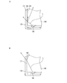
- FIG. 7A is a diagram showing an optical path of light from a light source (for example, LED) 180 in a conventional illumination device in which a light guide plate 160 and a frame 170 that are separately created are assembled.
- a gap 185 is formed between the end surface 161 around the light guide plate 160 and the inner peripheral surface 171 of the frame 170.
- Most of the light L emitted from the light source 180 and incident on the end surface 161 of the light guide plate 160 is totally reflected by the end surface 161 toward the light guide plate 160, and the rest passes through the end surface 161.
- the light emitted from the end surface 161 of the light guide plate 160 is incident on the inner peripheral surface 171 of the frame 170, a part of the light is reflected and enters the light guide plate 160, and the rest passes through the inner peripheral surface 171 and enters the frame 170. Is incident on.
- the gap 185 is formed between the end surface 161 of the light guide plate 160 and the inner peripheral surface 171 of the frame 170, most of the light L incident on the end surface 161 can be totally reflected. As a result, a decrease in luminance of the lighting device can be reduced.
- FIG. 7B shows the optical path of light from the light source (for example, LED) 180 in the lighting device in which the frame 170 is integrated with the light guide plate 160 by two-color molding, as in the lighting device shown in FIG. FIG.
- the end surface 161 of the light guide plate 160 and the inner peripheral surface 171 of the frame 170 are joined, and there is almost no difference in refractive index between the light guide plate 160 and the frame 170.
- Most of the light L incident on the interface between the optical plate 160 and the frame 170 passes through the interface and enters the frame 170, resulting in light loss.
- the interface between the end surface 161 of the light guide plate 160 and the inner peripheral surface 171 of the frame 170 is not a uniform flat surface, the reflectance of light at the interface further decreases, resulting in light loss.
- the loss of light is large, and the luminance of the lighting device is lowered.
- gaps 142 and 152 are formed between the light guide plate 140 and the frame 150. Therefore, as in FIG. 7A, much of the light incident on the end face of the light guide plate 140 that is in contact with the gaps 142 and 152 can be totally reflected.
- the lighting device of FIG. 6 also has a problem that the loss of light is large and the luminance of the lighting device is lowered. Moreover, in order to ensure the intensity
- An object of the present invention is to solve the above-described problems of the conventional lighting device, and to reduce the thickness and weight of the lighting device and the display device without reducing the strength and the luminance.
- the illuminating device of the present invention has a substantially rectangular light guide plate having at least one end surface as a light incident surface, a frame disposed so as to surround the light guide plate, and the light incident surface of the light guide plate. And a light source disposed between the light guide plate and the frame, wherein the light guide plate and the frame are integrally formed by two-color molding, At least a part of the end surface excluding the light incident surface is separated from the frame.
- a display device includes the above-described illumination device according to the present invention.
- the light guide plate and the frame are integrally formed by two-color molding.
- the display device of the present invention includes the above-described illumination device, it is possible to realize a thin, light and bright screen display device while ensuring the necessary strength.
- FIG. 1 is a cross-sectional view showing a schematic configuration of a liquid crystal display device according to an embodiment of the present invention.
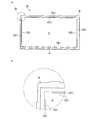
- 2A is a plan view showing a schematic configuration of a frame with a light guide plate constituting the illumination device used in the liquid crystal display device of FIG. 1
- FIG. 2B is an enlarged plan view of a portion 2B of FIG. 2A.
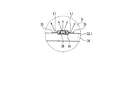
- FIG. 3 is an enlarged plan view showing the vicinity of the light source of the frame with the light guide plate constituting the liquid crystal display device of the present invention.
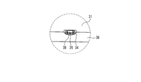
- FIG. 4 is an enlarged plan view showing the vicinity of the light source of another frame with a light guide plate constituting the liquid crystal display device of the present invention.
- FIG. 5 is an exploded perspective view showing a conventional lighting device.
- FIG. 6 is a perspective view showing a main part of another conventional lighting device.
- FIG. 7A is a diagram showing an optical path of light from a light source in a conventional lighting device in which a light guide plate and a frame are separate components
- FIG. 7B is a diagram in which the frame is integrated around the light guide plate by two-color molding. It is the figure which showed the optical path of the light from a light source in the conventional illuminating device.
- the light guide plate and the frame are integrally formed by two-color molding, and at least a part of the end surface of the light guide plate excluding the light incident surface is separated from the frame. That the light guide plate and the frame are “separated” means that they are not in contact with each other. Accordingly, for example, the case where the light guide plate 140 and the frame 150 are joined in the thickness direction as shown in FIG. 6 is not included. Although it can be arbitrarily set in which part the end face of the light guide plate is separated from the frame, it is preferably set in consideration of luminance unevenness, strength, and the like of the lighting device.
- an end surface of the light guide plate excluding the light incident surface is joined to the frame at at least one of four corner portions of the light guide plate having a substantially rectangular shape, and the frame is formed at other portions. It is preferable that it is separated from.
- the “corner portion” means a portion including four vertices of a substantially rectangular light guide plate when the light guide plate is viewed from a direction perpendicular to the main surface of the light guide plate. Light that propagates while being totally reflected inside the light guide plate is likely to gather at the corner portion, so even if the corner portion of the light guide plate is joined to the frame, the decrease in luminance at the corner portion should be relatively reduced. Can do. Therefore, it is possible to easily obtain a lighting device with uniform luminance.
- the light incident surface of the light guide plate may be joined to the frame except for a slot into which the light source is inserted. Thereby, intensity
- the light incident surface of the light guide plate may be separated from the frame in the vicinity of the slot in which the light source is inserted so that light emitted from the light source and incident on the light guide plate is totally reflected. Good. As a result, light entering the frame from the light guide plate in the vicinity of the slot can be reduced, so that a decrease in luminance of the lighting device can be further reduced.
- a concave curved surface is formed in a region of the frame facing the light source.
- the light from the light source can be reflected by the concave curved surface and incident on the light guide plate, so that the loss of light is reduced and the decrease in the luminance of the lighting device can be further reduced. Further, it is possible to suppress the occurrence of luminance unevenness in which only the vicinity of the light source becomes particularly bright.
- the light guide plate and the frame include the same material as a main component.
- Consisting as a main component means that the component is preferably contained in an amount of 50% by weight or more, more preferably 80% by weight or more.
- FIG. 1 is a cross-sectional view showing a schematic configuration of a liquid crystal display device 1 according to an embodiment of the present invention.
- the liquid crystal display device 1 includes a transmissive liquid crystal panel 10 as a display unit, and an edge light type illumination device 20 that is disposed on the back side of the liquid crystal panel 10 and illuminates the liquid crystal panel 10.
- the liquid crystal panel 10 includes an active substrate 11 in which a large number of pixel electrodes are arranged in a matrix, a counter substrate 12 in which a transparent electrode that faces the large number of pixel electrodes on the active substrate 11 is formed, and a space between the substrates 11 and 12. And a liquid crystal (not shown) sealed.
- an active substrate 11 in which a large number of pixel electrodes are arranged in a matrix
- a counter substrate 12 in which a transparent electrode that faces the large number of pixel electrodes on the active substrate 11 is formed
- a liquid crystal (not shown) sealed.
- the illuminating device 20 includes a light guide plate-equipped frame 30 in which a light guide plate 31 and a frame 36 are integrated, an optical sheet 22 laminated on a liquid crystal panel 10 side surface (light emitting surface) of the light guide plate 31, and a light guide plate.
- the optical sheet 22 is for, for example, aligning the polarization direction and the emission direction of light emitted from the surface of the light guide plate 31 on the liquid crystal panel 10 side, and making the luminance uniform.
- the optical sheet 22 may be comprised with the single sheet
- the reflection sheet 24 is for making the light leaked from the light guide plate 31 re-enter the light guide plate 31 to effectively use the light.
- the configuration of the reflection sheet 24 is not particularly limited, and any optical sheet used for, for example, an illumination device can be used.
- the reflection sheet 24 may be comprised with the single sheet
- FIG. 2A is a plan view showing a schematic configuration of the frame 30 with a light guide plate.
- the light guide plate-equipped frame 30 includes a light guide plate 31 and a frame 36 integrally formed around the light guide plate 31 by two-color molding.
- the light guide plate 31 is a plate-like body made of a transparent synthetic resin such as an acrylic resin (for example, PMMA).
- the light guide plate 31 includes a pair of substantially rectangular main surfaces facing each other and four peripheral end surfaces connecting the pair of main surfaces.
- One of the pair of main surfaces (light emission surface) is disposed to face the liquid crystal panel 10.
- the pair of end surfaces along the long side of the light guide plate 31 are referred to as long side end surfaces 32L1, 32L2, and the pair of end surfaces along the short side are referred to as short side end surfaces 32S1, 32S2.
- the frame 36 has a substantially rectangular frame shape, and is disposed around the light guide plate 31 so as to face the four end faces 32L1, 32L2, 32S1, and 32S2 of the light guide plate 31.
- the material of the frame 36 is not particularly limited, but preferably includes the same material as the light guide plate 31 as a main component. Thereby, since the dimensional change amount of the light-guide plate 31 and the frame 36 by environmental changes, such as temperature and humidity, becomes substantially the same, the reliability of the illuminating device 20 improves.
- the frame 36 may contain an optional additive such as a colorant (for example, particles) as necessary.
- a plurality of slots 34 are formed at substantially the same pitch between the light guide plate 31 and the frame 36 along one long side end surface 32L1 of the light guide plate 31.
- the slot 34 is a through hole, and an LED (not shown) serving as a light source of the lighting device 20 is inserted therein. That is, the long side end surface 32L1 of the light guide plate 31 is a light incident surface on which light from the LED is incident. The light emitted from the LED enters the long-side end surface 32L1 of the light guide plate 31, is diffused by propagating through the light guide plate 31 while being totally reflected, and is emitted from the main surface facing the liquid crystal panel 10.
- the number and interval of the slots 34 can be appropriately set according to the size of the lighting device.
- FIG. 2B is an enlarged plan view of the corner portion of the light guide plate 31 and the vicinity thereof sandwiched between the long-side end surface 32L2 and the short-side end surface 32S1 that are not light incident surfaces in FIG. 2A.
- the light guide plate 31 and the frame 36 are joined at the corner portion of the light guide plate 31, but are separated at other portions.
- detailed illustration is omitted, the same applies to the corner portion of the light guide plate 31 sandwiched between the long side end surface 32L2 and the short side end surface 32S2 and the vicinity thereof.
- the three end surfaces excluding the long side end surface 32L1 that is the light incident surface are the long side end surfaces 32L2 facing the light incident surface. It is separated from the frame 36 except for the corners at both ends.
- the light guide plate 31 and the frame 36 are joined by two-color molding except for the gaps 33L2, 33S1, 33S2 and the plurality of slots 34. Therefore, the strength of the light guide plate-equipped frame 30 is improved, and the strength of the lighting device 20 is improved. As a result, the lighting device 20 can be further reduced in thickness and weight. Further, since the width of the frame 36 can be reduced, the area around the display screen of the liquid crystal display device 1 (so-called frame area) can be reduced.
- the two-color molding method of the light guide plate 31 and the frame 36 there is no particular limitation on the two-color molding method of the light guide plate 31 and the frame 36.
- the light guide plate 31 is firstly molded using a primary mold, and then the frame 36 is secondarily molded so that the light guide plate 31 is installed in the secondary mold and integrated with the light guide plate 31. That's fine.
- the portion where the light guide plate 31 and the frame 36 are separated is not limited to the above embodiment. It is only necessary that the light guide plate 31 and the frame 36 be separated from each other on at least a part of the end surface excluding the light incident surface (long side end surface 32L1) of the light guide plate 31.
- the end surface around the light guide plate 31 may be separated from the frame 36 at four corners and joined to the frame 36 at other portions.
- the light guide plate 31 and the frame 36 are at least one of the four corners of the light guide plate 31 and the frame 36. It is preferable to join and separate at other portions.
- the light guide plate 31 and the frame 36 are separated at the corner portions at both ends of the light incident surface (long side end surface 32L1), but they may be joined at these corner portions.
- the light incident surface on which the light source is disposed is only the long side end surface 32L1, but the present invention is not limited to this.
- the light incident surface may be any of the four end surfaces of the light guide plate 31.
- the light incident surface is not limited to one of the four end surfaces of the light guide plate 31, and two or three of the four end surfaces can be used as the light incident surface. Regardless of which of the four end surfaces of the light guide plate 31 is the light incident surface, it is only necessary that at least a part of the end surface other than the light incident surface is separated from the frame 36.
- the light incident surface (long side end surface 32L1) of the light guide plate 31 is joined to the frame 36 except for the slot 34 into which the LED is inserted.
- This is advantageous in improving the strength of the light guide plate-equipped frame 30 because the joining region between the light guide plate 31 and the frame 36 is enlarged.
- the present invention is not limited to this.
- a gap 35 may be formed between the light guide plate 31 and the frame 36 in the vicinity of the slot 34 into which the LED 26 is inserted.
- the light L1 emitted from the LED 26 in an oblique direction and reflected by the end face portion of the light guide plate 31 facing the LED 26 is then incident on the light guide plate 31 at the end face portion of the light guide plate 31 in contact with the gap 35. It can be totally reflected. Therefore, the loss of light can be reduced and the luminance of the lighting device 20 can be improved.
- the gap 35 is formed only in the vicinity of the slot 34, but the gap 35 may be formed so as to connect the adjacent slots 34.
- a concave curved surface 38 may be formed in a region where the LED 26 of the frame 36 faces, that is, a region of the frame 36 constituting the slot 34.
- an arbitrary curved surface such as a cylindrical surface, a spherical surface, or an aspherical surface can be used.
- the concave curved surface 38 By causing the concave curved surface 38 to function as a reflective surface that reflects light emitted from the LED 26 to the periphery toward the light guide plate 31, the loss of light can be reduced and the luminance of the lighting device 20 can be improved. Further, it is possible to prevent the occurrence of luminance unevenness in which only the vicinity of the LED 26 becomes particularly bright.
- the gap 35 shown in FIG. 3 may be formed between the light guide plate 31 and the frame 36.
- an LED is used as the light source.
- the light source of the present invention is not limited to this, and any discharge fluorescent tube (cold cathode fluorescent tube, hot cathode fluorescent tube, xenon fluorescent tube, etc.), EL element, etc.
- the light source can be used.
- the lighting device of the present invention may further include a member made of a metal plate by press molding or the like in consideration of reinforcement, assembling to a display device, or the like.
- the illumination device of the present invention can also be used for applications other than the backlight device of a transmissive liquid crystal display device as shown in the above embodiment.
- it can be applied to lighting devices such as Xiaokasten, which irradiates X-rays with light, light boxes that irradiate light to photographic negatives, etc., and various signs installed indoors or outdoors, advertisements, information signs, etc. be able to.
- the configuration of each part of the lighting device can be changed as appropriate according to the application of the lighting device.
- the display device of the present invention only needs to include the illumination device of the present invention, and may be any display device that requires illumination light.
- the display device may display either a moving image or a still image.
- the application field of the present invention is not particularly limited, but can be particularly preferably used for a transmissive or transflective display panel.
Landscapes
- Physics & Mathematics (AREA)
- General Physics & Mathematics (AREA)
- Optics & Photonics (AREA)
- Engineering & Computer Science (AREA)
- Signal Processing (AREA)
- Planar Illumination Modules (AREA)
Abstract
照明装置(20)は、少なくとも一端面(32L1)を光入射面とする略矩形状の導光板(31)と、導光板の周囲を取り囲むように配置されたフレーム(36)と、導光板の光入射面に対向して、導光板とフレームとの間に配置された光源(26)とを備える。導光板とフレームとは二色成形により一体的に成形されており、導光板の光入射面を除く端面の少なくとも一部がフレームから離間している。これにより、強度及び輝度を低下させることなく、照明装置を薄型化・軽量化することができる。
Description
本発明は照明装置、特に導光板を備えた照明装置に関する。また、本発明は、このような照明装置を備えた表示装置に関する。
近年、携帯電話やノート型PC、PDAなどのモバイル機器などで使用される小型の液晶表示装置はもちろんのこと、テレビなどで使用される大型の液晶表示装置にまで幅広い範囲で液晶表示装置の薄型化・軽量化が進んでいる。
液晶表示装置では、液晶パネルの背面側に照明装置(バックライト装置)が配置され、使用者は、この照明装置から出射し、液晶パネルを通過した光を観察する。
上記照明装置は、液晶パネルに対する光源の配置の仕方により直下型とエッジライト型に大別される。エッジライト型では、略矩形の光出射面を備える導光板の周囲の一端面に対向して光源が配置される。光源から出射した光は、導光板の端面に入射し、導光板の一対の主面のうちの一方である光出射面から出射し、液晶パネルを照明する。
エッジライト型照明装置を薄型化・軽量化する場合、当該照明装置を構成する各部材を単に薄型化・軽量化したのでは、強度の低下が懸念される。そこで、強度の低下を防ぎつつ薄型化・軽量化するために、従来は別個の部材であった導光板とフレームとを二色成形(ダブルモールド)にて一体化させる技術が提案されている。
例えば、特許文献1には、図5に示すように、導光板110の周囲に矩形枠状のフレーム120が隙間なく密着するように、導光板110にフレーム120を二色成形により一体成形した照明装置が記載されている。図5において、参照符号130は導光板110の短辺側の端面に対向するように配置される線状光源、参照符号136は反射シート、参照符号137は調光シートである。
また、特許文献2には、図6に示すように、導光板140の周囲にフレーム150を二色成形により一体成形した照明装置が記載されている。導光板140の外周面にフランジ部141を形成し、フレーム150の内周面にフランジ受け部151を形成し、フランジ部141の上面とフランジ受け部151の下面とが接合される。導光板140のフランジ部141の先端とフレーム150の内周面との間、及び、導光板140の外周面とフレーム150のフランジ受け部151の先端との間には、それぞれ隙間142,152が形成されている。
図5及び図6のように、導光板にフレームを二色成形により一体化させた場合は、別個に作成した導光板とフレームとを組み立てた場合に比べて、強度を向上させることができるが、得られる照明装置の輝度が低下するという課題がある。これを図7A及び図7Bを用いて説明する。
図7Aは別々に作成した導光板160とフレーム170とを組み立てた従来の照明装置において光源(例えばLED)180からの光の光路を示した図である。この照明装置においては、導光板160の周囲の端面161とフレーム170の内周面171との間に隙間185が形成されている。光源180から出射し導光板160の端面161に入射した光Lの多くは端面161で導光板160内に向かって全反射され、残りは端面161を通過する。導光板160の端面161から出射した光は、フレーム170の内周面171に入射し、その一部は反射されて導光板160に入射し、残りは内周面171を通過してフレーム170内に入射する。このように、導光板160の端面161とフレーム170の内周面171との間に隙間185が形成されていると、端面161に入射した光Lの多くを全反射させることができるので、光の損失が少なくなり、その結果、照明装置の輝度の低下を少なくすることができる。
これに対して、図7Bは、図5に示した照明装置と同様に、導光板160にフレーム170が二色成形により一体化された照明装置において光源(例えばLED)180からの光の光路を示した図である。この照明装置では、導光板160の端面161とフレーム170の内周面171とが接合されており、しかも導光板160とフレーム170との屈折率差がほとんどないために、光源180から出射し導光板160とフレーム170との間の界面に入射した光Lの多くは、当該界面を通過してフレーム170内に入射し、光の損失となる。また、導光板160の端面161とフレーム170の内周面171との界面が均一な平坦面でない場合には、当該界面での光の反射率が更に低下して、光の損失となる。このように、導光板160にフレーム170を隙間なく密着させて二色成形した場合には、光の損失が多く、照明装置の輝度が低下してしまう。
図6に示した照明装置では、導光板140とフレーム150との間に隙間142,152が形成されている。従って、図7Aと同様に、隙間142,152に接する導光板140の端面に入射した光の多くを全反射させることができる。しかしながら、フランジ部141の上面はフランジ受け部151の下面と接合されているので、フランジ部141の上面に入射した光の多くはフランジ受け部151に入射し、光の損失となってしまう。従って、図6の照明装置でも、光の損失が多く、照明装置の輝度が低下してしまうという課題を有している。また、フランジ部141及びフランジ受け部151の強度を確保するためには、これらを薄くすることができない。従って、照明装置を薄型化することは困難である。
本発明は、上記の従来の照明装置の課題を解決し、強度及び輝度を低下させることなく照明装置及び表示装置を薄型化・軽量化することを目的とする。
本発明の照明装置は、少なくとも一端面を光入射面とする略矩形状の導光板と、前記導光板の周囲を取り囲むように配置されたフレームと、前記導光板の前記光入射面に対向して、前記導光板と前記フレームとの間に配置された光源とを備えた照明装置であって、前記導光板と前記フレームとが二色成形により一体的に成形されており、前記導光板の前記光入射面を除く端面の少なくとも一部が前記フレームから離間していることを特徴とする。
本発明の表示装置は、上記の本発明の照明装置を備えることを特徴とする。
本発明の照明装置では、導光板とフレームとが二色成形により一体的に成形されている。これにより、別個に作成した導光板とフレームとを組み立てる従来の照明装置に比べて、強度が向上する。その結果、照明装置の薄型化・軽量化が可能となる。
一方、導光板の光入射面を除く端面の少なくとも一部がフレームから離間している。これにより、導光板の端面のフレームから離間した部分に導光板内から入射した光の多くは導光板内に向かって全反射される。従って、光損失が少なくなり、照明装置の輝度の低下を防止することができる。
本発明の表示装置は、上記の照明装置を備えるので、必要な強度を確保したまま、薄型且つ軽量で、明るい画面の表示装置を実現できる。
本発明の照明装置では、導光板とフレームとが二色成形により一体的に成形されており、導光板の光入射面を除く端面の少なくとも一部がフレームから離間している。導光板とフレームとが「離間している」とは、両者が接触していないことを意味する。従って、例えば図6のように導光板140とフレーム150とが厚さ方向に接合されている場合は含まれない。いずれの部分で導光板の端面とフレームとを離間させるかは任意に設定することができるが、照明装置の輝度ムラや強度等を考慮して設定することが好ましい。
具体的には、前記導光板の前記光入射面を除く端面は、略矩形状の前記導光板の4つのコーナー部のうちの少なくとも1つで前記フレームと接合され、それ以外の部分で前記フレームから離間していることが好ましい。「コーナー部」とは、導光板の主面と垂直な方向から導光板を見たとき、略矩形の導光板の4つの頂点を含む部分を意味する。コーナー部には、導光板内を全反射しながら伝播する光が集まりやすいので、導光板のコーナー部がフレームと接合されていても、当該コーナー部での輝度の低下を相対的に少なくすることができる。従って、輝度が均一化な照明装置を容易に得ることができる。
前記導光板の前記光入射面は、前記光源が挿入されるスロットを除いて前記フレームと接合されていてもよい。これにより、強度を更に向上させることができる。
あるいは、前記導光板の前記光入射面は、前記光源から出射し前記導光板に入射した光が全反射されるように、前記光源が挿入されるスロットの近傍において前記フレームから離間していてもよい。これにより、スロットの近傍において導光板からフレーム内に入る光を少なくすることができるので、照明装置の輝度の低下を更に少なくすることができる。
前記フレームの前記光源に対向する領域に凹曲面が形成されていることが好ましい。これにより、光源からの光を凹曲面で反射させて導光板に入射させることができるので、光の損失が少なくなり、照明装置の輝度の低下を更に少なくすることができる。また、光源の近傍部分だけが特に明るくなる輝度ムラの発生を抑えることができる。
前記導光板と前記フレームとが同一材料を主成分として含むことが好ましい。これにより、導光板とフレームとで温度や湿度などの環境変化による寸法変化量が略同一になるので、照明装置の信頼性が向上する。「主成分として含む」とは、当該成分を好ましくは50重量%以上、更に好ましくは80重量%以上含むことをいう。
以下、本発明を好適な実施形態を示しながら詳細に説明する。但し、本発明は以下の実施形態に限定されないことはいうまでもない。以下の説明において参照する各図は、説明の便宜上、本発明の実施形態の構成部材のうち、本発明を説明するために必要な主要部材のみを簡略化して示したものである。従って、本発明は以下の各図に示されていない任意の構成部材を備え得る。また、以下の各図中の部材の寸法は、実際の構成部材の寸法および各部材の寸法比率等を忠実に表したものではない。
図1は、本発明の一実施形態に係る液晶表示装置1の概略構成を示した断面図である。この液晶表示装置1は、表示部としての透過型の液晶パネル10と、液晶パネル10の背面側に配置されて液晶パネル10を照明するエッジライト型の照明装置20とを備える。
液晶パネル10は、多数の画素電極がマトリクス状に配置されたアクティブ基板11と、アクティブ基板11の多数の画素電極に対向する透明電極が形成された対向基板12と、これら基板11,12の間に封止された液晶(図示せず)とを備える。多数の画素電極の各電位を制御することで、照明装置20からの照明光の通過を画素単位で制御する。アクティブ基板11及び対向基板12の液晶とは反対側の各面には偏向フィルム13,14が積層されている。液晶パネル10は、両面接着テープ15で、フレーム36に固定されている。
照明装置20は、導光板31とフレーム36とが一体化された導光板付きフレーム30と、導光板31の液晶パネル10側の面(光出射面)に積層された光学シート22と、導光板31の液晶パネル10とは反対側の面に接着された反射シート24とを備える。
光学シート22は、例えば導光板31の液晶パネル10側の面から出射した光の偏光方向や出射方向を揃えたり、輝度を均一化させたりするためのものである。光学シート22の構成は特に制限はなく、例えば照明装置に使用される任意の光学シートを用いることができる。また、光学シート22は、単一のシートで構成されていてもよいし、複数のシートで構成されていてもよい。
反射シート24は、導光板31から漏れ出た光を導光板31に再入射させて光の有効利用を図るためのものである。反射シート24の構成も特に制限はなく、例えば照明装置に使用される任意の光学シートを用いることができる。また、反射シート24は、単一のシートで構成されていてもよいし、複数のシートで構成されていてもよい。
図2Aは導光板付きフレーム30の概略構成を示した平面図である。導光板付きフレーム30は、導光板31と、導光板31の周囲に二色成形により一体成形されたフレーム36とを備える。
導光板31は、アクリル樹脂(例えばPMMA)などの透明な合成樹脂からなる板状体である。導光板31は、互いに対向する略矩形状の一対の主面と、一対の主面を繋ぐ周囲の4つの端面とを備える。一対の主面のうちの一方(光出射面)は液晶パネル10に対向して配置される。4つの端面のうち、導光板31の長辺に沿った一対の端面を長辺側端面32L1,32L2、短辺に沿った一対の端面を短辺側端面32S1,32S2と呼ぶ。
フレーム36は、略矩形枠形状を有し、導光板31の4つの端面32L1,32L2,32S1,32S2に対向するように、導光板31の周囲に配置されている。フレーム36の材料は特に制限はないが、好ましくは導光板31と同一材料を主成分として含むことが好ましい。これにより、温度や湿度などの環境変化による導光板31及びフレーム36の寸法変化量が略同一になるので、照明装置20の信頼性が向上する。フレーム36は、必要に応じて着色剤(例えば粒子)等の任意の添加剤を含んでいてもよい。
導光板31の一方の長辺側端面32L1に沿って、導光板31とフレーム36との間に複数のスロット34が略同一ピッチで形成されている。スロット34は貫通穴であり、照明装置20の光源となるLED(図示せず)が挿入される。即ち、導光板31の長辺側端面32L1は、LEDからの光が入射する光入射面である。LEDから出射された光は導光板31の長辺側端面32L1に入射し、導光板31内を全反射しながら伝播することで拡散され、液晶パネル10に対向する主面から出射する。スロット34の数や間隔は、照明装置のサイズ等に応じて適宜設定することができる。
導光板31の4つの端面のうち、光入射面である長辺側端面32L1を除く3つの端面(即ち、長辺側端面32L2,短辺側端面32S1,32S2)には、導光板31とフレーム36との間に隙間33L2,33S1,33S2が形成されている。図2Aにおいて、二色成形により接合された導光板31とフレーム36との境界を破線で示している。
図2Bは、図2Aにおいて、光入射面ではない長辺側端面32L2と短辺側端面32S1とで挟まれた導光板31のコーナー部及びその近傍の拡大平面図である。図2Bに示すように、導光板31とフレーム36とは、導光板31の当該コーナー部では接合されているが、それ以外の部分では離間している。詳細な図示を省略するが、長辺側端面32L2と短辺側端面32S2とで挟まれた導光板31のコーナー部及びその近傍でも同様である。
以上のように、本実施形態では、導光板31の4つの端面のうち、光入射面である長辺側端面32L1を除いた3つの端面は、光入射面と対向する長辺側端面32L2の両端のコーナー部を除いて、フレーム36と離間している。これにより、図7Aで説明したのと同様に、LEDから導光板31内に入射し、隙間33L2,33S1,33S2と接する導光板31の端面の部分に入射した光の多くは導光板31内に向かって全反射される。したがって、照明装置20の輝度の低下を少なくすることができる。即ち、別個に作成した導光板とフレームとを組み立てた従来の照明装置と同等の輝度を確保することができる。
一方、導光板31とフレーム36とは、隙間33L2,33S1,33S2及び複数のスロット34を除いて二色成形により接合されている。したがって、導光板付きフレーム30の強度が向上し、また照明装置20の強度が向上する。その結果、照明装置20の更なる薄型化・軽量化が可能となる。また、フレーム36の幅を狭くすることができるので、液晶表示装置1の表示画面の周囲の領域(いわゆる額縁領域)を狭くすることが可能となる。
導光板31とフレーム36との二色成形の方法は特に制限はない。例えば、最初に一次金型を用いて導光板31を一次成形し、次いで、導光板31を二次金型内に設置して導光板31と一体化されるようにフレーム36を二次成形すればよい。
上記の実施形態は例示であって、本発明は上記の実施形態に限定されず、適宜変更することができる。
例えば、導光板31とフレーム36とが離間する部分は、上記の実施形態に限定されない。導光板31の光入射面(長辺側端面32L1)を除く端面の少なくとも一部で、導光板31とフレーム36とが離間していればよい。例えば、導光板31の周囲の端面を、4つのコーナー部でフレーム36と離間させ、それ以外の部分でフレーム36と接合してもよい。但し、導光板31の光出射面の輝度を確保し且つ均一化させるためには、一般には、導光板31とフレーム36とは、導光板31の4つのコーナー部の少なくとも1つでフレーム36と接合し、それ以外の部分で離間させることが好ましい。
上記の実施形態では、光入射面(長辺側端面32L1)の両端のコーナー部で導光板31とフレーム36とは離間していたが、これらのコーナー部でも両者を接合してもよい。
上記の実施形態では、光源が配置される光入射面は長辺側端面32L1のみであったが、本発明はこれに限定されない。光入射面は、導光板31の4つの端面のいずれであってもよい。光入射面は導光板31の4つの端面のうちの1面に限定されず、4つの端面のうちの2面又は3面を光入射面とすることができる。導光板31の4つの端面のうちのいずれが光入射面であっても、光入射面以外の端面の少なくとも一部が、フレーム36から離間していればよい。
上記の実施形態では、導光板31の光入射面(長辺側端面32L1)のうち、LEDが挿入されるスロット34以外の部分はフレーム36と接合されていた。これは、導光板31とフレーム36との接合領域が拡大するので、導光板付きフレーム30の強度を向上させるのに有利である。しかしながら、本発明はこれに限定されない。例えば、図3に示すように、LED26が挿入されるスロット34の近傍において、導光板31とフレーム36との間に隙間35を形成してもよい。これにより、LED26から斜め方向に出射し、LED26に対向する導光板31の端面の部分で反射された後、導光板31に入射した光L1を、隙間35と接する導光板31の端面の部分で全反射させることができる。したがって、光の損失を少なくし、照明装置20の輝度を向上させることができる。図3では、隙間35をスロット34の近傍部分のみに形成したが、隣り合うスロット34間を繋ぐように隙間35を形成してもよい。
図4に示すように、フレーム36のLED26が対向する領域、即ち、スロット34を構成するフレーム36の領域に、凹曲面38を形成してもよい。凹曲面38としては、円筒面、球面、非球面など任意の曲面を用いることができる。凹曲面38を、LED26から周囲に発射された光を導光板31に向かって反射させる反射面として機能させることで、光の損失を少なくし、照明装置20の輝度を向上させることができる。また、LED26の近傍部分のみが特に明るくなる輝度ムラの発生を防止できる。図4において、図3に示した隙間35を導光板31とフレーム36との間に形成してもよい。
上記の実施形態では、光源としてLEDを用いたが、本発明の光源はこれに限定されず、放電蛍光管(冷陰極蛍光管、熱陰極蛍光管、キセノン蛍光管など)、EL素子等の任意の光源を用いることができる。
本発明の照明装置は、補強や表示装置への組み立て性等を考慮して、金属板をプレス成形等により作成した部材を更に含んでいてもよい。
本発明の照明装置は、上記の実施形態で示したような透過型の液晶表示装置のバックライト装置以外の用途に使用することもできる。例えば、レントゲン写真に光を照射するシャウカステン、写真ネガ等に光を照射して視認をし易くするライトボックス、屋内又は屋外に設置される各種看板、広告、案内標識などの照明装置にも適用することができる。照明装置の用途に応じて照明装置の各部の構成を適宜変更することができる。
本発明の表示装置は、本発明の照明装置を備えていれば良く、照明光を必要とする任意の表示装置であってもよい。表示装置は、動画・静止画のいずれを表示するものであってもよい。
以上に説明した実施形態は、いずれもあくまでも本発明の技術的内容を明らかにする意図のものであって、本発明はこのような具体例にのみ限定して解釈されるものではなく、その発明の精神と請求の範囲に記載する範囲内でいろいろと変更して実施することができ、本発明を広義に解釈すべきである。
本発明の利用分野は、特に制限はないが、透過型または半透過型表示パネルに特に好ましく利用することができる。
1 液晶表示装置
10 液晶パネル
11 アクティブ基板
12 対向基板
12,13 偏光フィルム
15 両面接着テープ
20 照明装置
22 光学シート
24 反射シート
26 LED(光源)
30 導光板付きフレーム
31 導光板
33L2,33S1,33S2 隙間
34 スロット
35 隙間
36 フレーム
38 凹曲面
10 液晶パネル
11 アクティブ基板
12 対向基板
12,13 偏光フィルム
15 両面接着テープ
20 照明装置
22 光学シート
24 反射シート
26 LED(光源)
30 導光板付きフレーム
31 導光板
33L2,33S1,33S2 隙間
34 スロット
35 隙間
36 フレーム
38 凹曲面
Claims (7)
- 少なくとも一端面を光入射面とする略矩形状の導光板と、前記導光板の周囲を取り囲むように配置されたフレームと、前記導光板の前記光入射面に対向して、前記導光板と前記フレームとの間に配置された光源とを備えた照明装置であって、
前記導光板と前記フレームとが二色成形により一体的に成形されており、
前記導光板の前記光入射面を除く端面の少なくとも一部が前記フレームから離間していることを特徴とする照明装置。 - 前記導光板の前記光入射面を除く端面は、略矩形状の前記導光板の4つのコーナー部のうちの少なくとも1つで前記フレームと接合され、それ以外の部分で前記フレームから離間している請求項1に記載の照明装置。
- 前記導光板の前記光入射面は、前記光源が挿入されるスロットを除いて前記フレームと接合されている請求項1に記載の照明装置。
- 前記導光板の前記光入射面は、前記光源から出射し前記導光板に入射した光が全反射されるように、前記光源が挿入されるスロットの近傍において前記フレームから離間している請求項1に記載の照明装置。
- 前記フレームの前記光源に対向する領域に凹曲面が形成されている請求項1に記載の照明装置。
- 前記導光板と前記フレームとが同一材料を主成分として含む請求項1に記載の照明装置。
- 請求項1~6のいずれかに記載の照明装置を備える表示装置。
Priority Applications (1)
| Application Number | Priority Date | Filing Date | Title |
|---|---|---|---|
| US13/581,400 US20120320624A1 (en) | 2010-04-22 | 2011-03-31 | Illuminating device and display device |
Applications Claiming Priority (2)
| Application Number | Priority Date | Filing Date | Title |
|---|---|---|---|
| JP2010-098944 | 2010-04-22 | ||
| JP2010098944 | 2010-04-22 |
Publications (1)
| Publication Number | Publication Date |
|---|---|
| WO2011132515A1 true WO2011132515A1 (ja) | 2011-10-27 |
Family
ID=44834049
Family Applications (1)
| Application Number | Title | Priority Date | Filing Date |
|---|---|---|---|
| PCT/JP2011/058302 Ceased WO2011132515A1 (ja) | 2010-04-22 | 2011-03-31 | 照明装置及び表示装置 |
Country Status (2)
| Country | Link |
|---|---|
| US (1) | US20120320624A1 (ja) |
| WO (1) | WO2011132515A1 (ja) |
Families Citing this family (12)
| Publication number | Priority date | Publication date | Assignee | Title |
|---|---|---|---|---|
| ES2863539T3 (es) * | 2017-10-26 | 2021-10-11 | Signify Holding Bv | Un conjunto de módulo de iluminación |
| US10880394B2 (en) | 2018-03-04 | 2020-12-29 | Netskrt Systems, Inc. | Transparent cache system and method for transparently caching multimedia content from multiple content providers |
| US11140583B2 (en) | 2018-03-22 | 2021-10-05 | Netskrt Systems, Inc. | Transforming video manifests to enable efficient media distribution |
| US11375036B2 (en) | 2018-03-22 | 2022-06-28 | Netskrt Systems, Inc. | Method and apparatus to prioritize and schedule the distribution of learned content |
| US11128728B2 (en) | 2018-03-22 | 2021-09-21 | Netskrt Systems, Inc. | Method and apparatus for walled garden with a mobile content distribution network |
| US11252253B2 (en) | 2018-03-22 | 2022-02-15 | Netskrt Systems, Inc. | Caching aggregate content based on limited cache interaction |
| US11323536B2 (en) | 2018-03-22 | 2022-05-03 | Netskrt Systems, Inc. | Apparatus and method for trans-border movement of streaming media content |
| US11356530B2 (en) | 2018-03-22 | 2022-06-07 | Netskrt Systems, Inc. | Leveraging mobile environment to distribute cache data |
| US11388252B2 (en) | 2018-03-22 | 2022-07-12 | Netskrt Systems, Inc. | Micro-cache method and apparatus for a mobile environment with variable connectivity |
| US11399058B2 (en) | 2018-03-22 | 2022-07-26 | Netskrt Systems, Inc. | Immutable ledger method and apparatus for managing the distribution of content |
| WO2020024696A1 (zh) * | 2018-07-31 | 2020-02-06 | Oppo广东移动通信有限公司 | 显示屏组件、电子设备及电子设备的控制方法 |
| US12184907B2 (en) | 2021-06-04 | 2024-12-31 | Netskrt Systems, Inc. | Method and apparatus for multicast control of a live video stream |
Citations (6)
| Publication number | Priority date | Publication date | Assignee | Title |
|---|---|---|---|---|
| JPH08146420A (ja) * | 1994-11-21 | 1996-06-07 | Sony Corp | 液晶表示装置およびその照明装置の製造方法 |
| JP2002244575A (ja) * | 2000-12-13 | 2002-08-30 | Ryuichi Yoshitoshi | バックライト及びこれを用いた液晶表示装置 |
| JP2003295182A (ja) * | 2002-03-29 | 2003-10-15 | Sharp Corp | 液晶表示装置 |
| JP2004095516A (ja) * | 2002-09-04 | 2004-03-25 | Seiko Epson Corp | 導光体ユニット、バックライトユニット、電気光学装置、電子機器及び導光体ユニットの製造方法 |
| JP2004253306A (ja) * | 2003-02-21 | 2004-09-09 | Sanyo Electric Co Ltd | 面光源装置及びこれを用いた表示装置 |
| JP2004286777A (ja) * | 2003-03-19 | 2004-10-14 | Hitachi Displays Ltd | 液晶表示装置 |
-
2011
- 2011-03-31 WO PCT/JP2011/058302 patent/WO2011132515A1/ja not_active Ceased
- 2011-03-31 US US13/581,400 patent/US20120320624A1/en not_active Abandoned
Patent Citations (6)
| Publication number | Priority date | Publication date | Assignee | Title |
|---|---|---|---|---|
| JPH08146420A (ja) * | 1994-11-21 | 1996-06-07 | Sony Corp | 液晶表示装置およびその照明装置の製造方法 |
| JP2002244575A (ja) * | 2000-12-13 | 2002-08-30 | Ryuichi Yoshitoshi | バックライト及びこれを用いた液晶表示装置 |
| JP2003295182A (ja) * | 2002-03-29 | 2003-10-15 | Sharp Corp | 液晶表示装置 |
| JP2004095516A (ja) * | 2002-09-04 | 2004-03-25 | Seiko Epson Corp | 導光体ユニット、バックライトユニット、電気光学装置、電子機器及び導光体ユニットの製造方法 |
| JP2004253306A (ja) * | 2003-02-21 | 2004-09-09 | Sanyo Electric Co Ltd | 面光源装置及びこれを用いた表示装置 |
| JP2004286777A (ja) * | 2003-03-19 | 2004-10-14 | Hitachi Displays Ltd | 液晶表示装置 |
Also Published As
| Publication number | Publication date |
|---|---|
| US20120320624A1 (en) | 2012-12-20 |
Similar Documents
| Publication | Publication Date | Title |
|---|---|---|
| WO2011132515A1 (ja) | 照明装置及び表示装置 | |
| CN105425334B (zh) | 显示设备 | |
| US7360937B2 (en) | White light generating unit, backlight assembly having the same and liquid crystal display device having the same | |
| CN102022673B (zh) | 背光单元和具有该背光单元的液晶显示设备 | |
| KR101966739B1 (ko) | 곡면 디스플레이 장치 | |
| US20160216435A1 (en) | Curved display device | |
| KR100787355B1 (ko) | 양면 표시 장치 및 면광원 장치 | |
| CN101680637B (zh) | 照明装置和液晶显示装置 | |
| US8491169B2 (en) | Frame, light source device, display device, and television receiver | |
| JP2008204794A (ja) | 面状光源装置、及び表示装置 | |
| CN106104141A (zh) | 照明装置和显示装置 | |
| CN113687543B (zh) | 显示模组和显示装置 | |
| JP5604342B2 (ja) | 額縁被覆部材 | |
| CN103975192B (zh) | 背光源单元和液晶显示装置 | |
| CN105579764A (zh) | 照明装置以及显示装置 | |
| JP2019021474A (ja) | バックライト装置、およびこれを備える液晶表示装置 | |
| KR101824603B1 (ko) | 백라이트 유닛 및 이를 구비한 액정표시장치 | |
| US20140355304A1 (en) | Light source module, and liquid crystal display device | |
| CN114077093B (zh) | 侧入式光源、背光模组及显示装置 | |
| JP5459728B2 (ja) | 液晶表示装置 | |
| US8395719B2 (en) | Display device and light source block used therein | |
| JP2022023207A (ja) | 表示装置 | |
| CN110133921B (zh) | 显示装置 | |
| KR101690324B1 (ko) | 액정표시장치 | |
| JP2006330032A (ja) | 光学シートとそれを用いたバックライト・ユニットおよびディスプレイ |
Legal Events
| Date | Code | Title | Description |
|---|---|---|---|
| 121 | Ep: the epo has been informed by wipo that ep was designated in this application |
Ref document number: 11771852 Country of ref document: EP Kind code of ref document: A1 |
|
| WWE | Wipo information: entry into national phase |
Ref document number: 13581400 Country of ref document: US |
|
| NENP | Non-entry into the national phase |
Ref country code: DE |
|
| 122 | Ep: pct application non-entry in european phase |
Ref document number: 11771852 Country of ref document: EP Kind code of ref document: A1 |
|
| NENP | Non-entry into the national phase |
Ref country code: JP |