WO2011125416A1 - 液晶表示装置 - Google Patents
液晶表示装置 Download PDFInfo
- Publication number
- WO2011125416A1 WO2011125416A1 PCT/JP2011/055827 JP2011055827W WO2011125416A1 WO 2011125416 A1 WO2011125416 A1 WO 2011125416A1 JP 2011055827 W JP2011055827 W JP 2011055827W WO 2011125416 A1 WO2011125416 A1 WO 2011125416A1
- Authority
- WO
- WIPO (PCT)
- Prior art keywords
- display area
- liquid crystal
- pixel
- display
- electrode
- Prior art date
- Legal status (The legal status is an assumption and is not a legal conclusion. Google has not performed a legal analysis and makes no representation as to the accuracy of the status listed.)
- Ceased
Links
Images




Classifications
-
- G—PHYSICS
- G09—EDUCATION; CRYPTOGRAPHY; DISPLAY; ADVERTISING; SEALS
- G09G—ARRANGEMENTS OR CIRCUITS FOR CONTROL OF INDICATING DEVICES USING STATIC MEANS TO PRESENT VARIABLE INFORMATION
- G09G3/00—Control arrangements or circuits, of interest only in connection with visual indicators other than cathode-ray tubes
- G09G3/20—Control arrangements or circuits, of interest only in connection with visual indicators other than cathode-ray tubes for presentation of an assembly of a number of characters, e.g. a page, by composing the assembly by combination of individual elements arranged in a matrix no fixed position being assigned to or needed to be assigned to the individual characters or partial characters
- G09G3/34—Control arrangements or circuits, of interest only in connection with visual indicators other than cathode-ray tubes for presentation of an assembly of a number of characters, e.g. a page, by composing the assembly by combination of individual elements arranged in a matrix no fixed position being assigned to or needed to be assigned to the individual characters or partial characters by control of light from an independent source
- G09G3/36—Control arrangements or circuits, of interest only in connection with visual indicators other than cathode-ray tubes for presentation of an assembly of a number of characters, e.g. a page, by composing the assembly by combination of individual elements arranged in a matrix no fixed position being assigned to or needed to be assigned to the individual characters or partial characters by control of light from an independent source using liquid crystals
- G09G3/3611—Control of matrices with row and column drivers
- G09G3/3648—Control of matrices with row and column drivers using an active matrix
- G09G3/3666—Control of matrices with row and column drivers using an active matrix with the matrix divided into sections
-
- G—PHYSICS
- G02—OPTICS
- G02F—OPTICAL DEVICES OR ARRANGEMENTS FOR THE CONTROL OF LIGHT BY MODIFICATION OF THE OPTICAL PROPERTIES OF THE MEDIA OF THE ELEMENTS INVOLVED THEREIN; NON-LINEAR OPTICS; FREQUENCY-CHANGING OF LIGHT; OPTICAL LOGIC ELEMENTS; OPTICAL ANALOGUE/DIGITAL CONVERTERS
- G02F1/00—Devices or arrangements for the control of the intensity, colour, phase, polarisation or direction of light arriving from an independent light source, e.g. switching, gating or modulating; Non-linear optics
- G02F1/01—Devices or arrangements for the control of the intensity, colour, phase, polarisation or direction of light arriving from an independent light source, e.g. switching, gating or modulating; Non-linear optics for the control of the intensity, phase, polarisation or colour
- G02F1/13—Devices or arrangements for the control of the intensity, colour, phase, polarisation or direction of light arriving from an independent light source, e.g. switching, gating or modulating; Non-linear optics for the control of the intensity, phase, polarisation or colour based on liquid crystals, e.g. single liquid crystal display cells
- G02F1/133—Constructional arrangements; Operation of liquid crystal cells; Circuit arrangements
- G02F1/1333—Constructional arrangements; Manufacturing methods
- G02F1/1335—Structural association of cells with optical devices, e.g. polarisers or reflectors
- G02F1/133553—Reflecting elements
- G02F1/133555—Transflectors
-
- G—PHYSICS
- G02—OPTICS
- G02F—OPTICAL DEVICES OR ARRANGEMENTS FOR THE CONTROL OF LIGHT BY MODIFICATION OF THE OPTICAL PROPERTIES OF THE MEDIA OF THE ELEMENTS INVOLVED THEREIN; NON-LINEAR OPTICS; FREQUENCY-CHANGING OF LIGHT; OPTICAL LOGIC ELEMENTS; OPTICAL ANALOGUE/DIGITAL CONVERTERS
- G02F1/00—Devices or arrangements for the control of the intensity, colour, phase, polarisation or direction of light arriving from an independent light source, e.g. switching, gating or modulating; Non-linear optics
- G02F1/01—Devices or arrangements for the control of the intensity, colour, phase, polarisation or direction of light arriving from an independent light source, e.g. switching, gating or modulating; Non-linear optics for the control of the intensity, phase, polarisation or colour
- G02F1/13—Devices or arrangements for the control of the intensity, colour, phase, polarisation or direction of light arriving from an independent light source, e.g. switching, gating or modulating; Non-linear optics for the control of the intensity, phase, polarisation or colour based on liquid crystals, e.g. single liquid crystal display cells
- G02F1/133—Constructional arrangements; Operation of liquid crystal cells; Circuit arrangements
- G02F1/1333—Constructional arrangements; Manufacturing methods
- G02F1/133391—Constructional arrangement for sub-divided displays
-
- G—PHYSICS
- G02—OPTICS
- G02F—OPTICAL DEVICES OR ARRANGEMENTS FOR THE CONTROL OF LIGHT BY MODIFICATION OF THE OPTICAL PROPERTIES OF THE MEDIA OF THE ELEMENTS INVOLVED THEREIN; NON-LINEAR OPTICS; FREQUENCY-CHANGING OF LIGHT; OPTICAL LOGIC ELEMENTS; OPTICAL ANALOGUE/DIGITAL CONVERTERS
- G02F1/00—Devices or arrangements for the control of the intensity, colour, phase, polarisation or direction of light arriving from an independent light source, e.g. switching, gating or modulating; Non-linear optics
- G02F1/01—Devices or arrangements for the control of the intensity, colour, phase, polarisation or direction of light arriving from an independent light source, e.g. switching, gating or modulating; Non-linear optics for the control of the intensity, phase, polarisation or colour
- G02F1/13—Devices or arrangements for the control of the intensity, colour, phase, polarisation or direction of light arriving from an independent light source, e.g. switching, gating or modulating; Non-linear optics for the control of the intensity, phase, polarisation or colour based on liquid crystals, e.g. single liquid crystal display cells
- G02F1/133—Constructional arrangements; Operation of liquid crystal cells; Circuit arrangements
- G02F1/136—Liquid crystal cells structurally associated with a semi-conducting layer or substrate, e.g. cells forming part of an integrated circuit
- G02F1/1362—Active matrix addressed cells
- G02F1/136213—Storage capacitors associated with the pixel electrode
-
- G—PHYSICS
- G09—EDUCATION; CRYPTOGRAPHY; DISPLAY; ADVERTISING; SEALS
- G09G—ARRANGEMENTS OR CIRCUITS FOR CONTROL OF INDICATING DEVICES USING STATIC MEANS TO PRESENT VARIABLE INFORMATION
- G09G2300/00—Aspects of the constitution of display devices
- G09G2300/04—Structural and physical details of display devices
- G09G2300/0421—Structural details of the set of electrodes
- G09G2300/0426—Layout of electrodes and connections
-
- G—PHYSICS
- G09—EDUCATION; CRYPTOGRAPHY; DISPLAY; ADVERTISING; SEALS
- G09G—ARRANGEMENTS OR CIRCUITS FOR CONTROL OF INDICATING DEVICES USING STATIC MEANS TO PRESENT VARIABLE INFORMATION
- G09G2300/00—Aspects of the constitution of display devices
- G09G2300/04—Structural and physical details of display devices
- G09G2300/0439—Pixel structures
- G09G2300/0456—Pixel structures with a reflective area and a transmissive area combined in one pixel, such as in transflectance pixels
-
- G—PHYSICS
- G09—EDUCATION; CRYPTOGRAPHY; DISPLAY; ADVERTISING; SEALS
- G09G—ARRANGEMENTS OR CIRCUITS FOR CONTROL OF INDICATING DEVICES USING STATIC MEANS TO PRESENT VARIABLE INFORMATION
- G09G2300/00—Aspects of the constitution of display devices
- G09G2300/08—Active matrix structure, i.e. with use of active elements, inclusive of non-linear two terminal elements, in the pixels together with light emitting or modulating elements
- G09G2300/0809—Several active elements per pixel in active matrix panels
- G09G2300/0842—Several active elements per pixel in active matrix panels forming a memory circuit, e.g. a dynamic memory with one capacitor
-
- G—PHYSICS
- G09—EDUCATION; CRYPTOGRAPHY; DISPLAY; ADVERTISING; SEALS
- G09G—ARRANGEMENTS OR CIRCUITS FOR CONTROL OF INDICATING DEVICES USING STATIC MEANS TO PRESENT VARIABLE INFORMATION
- G09G2300/00—Aspects of the constitution of display devices
- G09G2300/08—Active matrix structure, i.e. with use of active elements, inclusive of non-linear two terminal elements, in the pixels together with light emitting or modulating elements
- G09G2300/0809—Several active elements per pixel in active matrix panels
- G09G2300/0842—Several active elements per pixel in active matrix panels forming a memory circuit, e.g. a dynamic memory with one capacitor
- G09G2300/0857—Static memory circuit, e.g. flip-flop
-
- G—PHYSICS
- G09—EDUCATION; CRYPTOGRAPHY; DISPLAY; ADVERTISING; SEALS
- G09G—ARRANGEMENTS OR CIRCUITS FOR CONTROL OF INDICATING DEVICES USING STATIC MEANS TO PRESENT VARIABLE INFORMATION
- G09G2330/00—Aspects of power supply; Aspects of display protection and defect management
- G09G2330/02—Details of power systems and of start or stop of display operation
- G09G2330/021—Power management, e.g. power saving
Definitions
- the present invention relates to a liquid crystal display device provided with a switching element for each pixel.
- FPD thin flat panel display
- Some FPDs use a liquid crystal, a light emitting diode (LED), an organic electroluminescence (EL), or the like as a display element.
- LED light emitting diode
- EL organic electroluminescence
- LCD liquid crystal display device
- liquid crystal display devices are mainly transmissive type in which a backlight is disposed on the back surface of the display panel and the backlight is turned on to perform transmissive display.
- the transmissive liquid crystal display device has a problem in that power consumption is large because the backlight needs to be constantly turned on. Therefore, a reflective liquid crystal display device that reflects external light as a display light source by providing a reflection plate inside the device or using a reflective electrode that reflects incident light from the outside as a pixel electrode is provided.
- the reflective liquid crystal display device light incident from the outside can be used as a display light source by reflecting the light inside the device, so that a backlight is not necessary. Therefore, the power consumption of the liquid crystal display device can be kept low.
- the reflective liquid crystal display device can be thinner and lighter than the transmissive liquid crystal display device, it is preferably used for mobile devices.
- a transflective liquid crystal display device has been disclosed as a liquid crystal display device having both reflective characteristics and transmissive characteristics.
- the transflective liquid crystal display device In the transflective liquid crystal display device, external light is incident from above and backlight light is incident from below. External light is reflected by the electrode, and backlight light passes through the electrode.
- the transflective liquid crystal display device includes a plurality of pixels each having a portion made of an electrode that transmits backlight light and a portion made of an electrode that reflects external light. Therefore, according to the transflective liquid crystal display device, the transmission mode display and the reflection mode display can be simultaneously performed by the transmitted light of the backlight and the reflected light of the external light.
- the backlight when the ambient light is bright, the backlight can be turned off and used as a reflective liquid crystal display device.
- the backlight can be turned on and used as a transmissive liquid crystal display device. is there. Therefore, according to the above configuration, the lighting time of the backlight can be reduced, so that power consumption can be suppressed as much as possible.
- liquid crystal display devices are widely used in electronic devices such as television receivers, personal computers, mobile phones, and digital cameras.
- mobile devices such as mobile phones and digital cameras have lower power consumption. Things are sought. From the viewpoint of low power consumption, reduction of power consumption of the display panel is an important issue. Therefore, in recent years, a technique for further reducing the power consumption of the liquid crystal display device has been developed.
- Patent Document 1 discloses a liquid crystal display device having two display areas. The details are shown in FIG. FIG. 9 is a plan view schematically showing the liquid crystal display device 30 disclosed in this document. Specifically, as shown in FIG. 9, there are two display areas, a reflective area 25a that performs display by the light reflection system and a reflection / transmission area 25b that performs display by using both the light reflection system and the light transmission system. Have.
- the pixel electrode in the reflection region 25a is obtained by patterning a conductive light reflection film into a predetermined shape, and the pixel electrode in the reflection / transmission region 25b has one or more openings that transmit incident light to the conductive light reflection film. It is provided and patterned into a predetermined shape.
- the backlight is disposed at a position corresponding to the reflection / transmission region 25b.
- the light from the backlight is used only in the reflection / transmission area 25b. Therefore, power consumption of the backlight can be reduced. Furthermore, the backlight may be disposed at a position where the reflection / transmission area 25b is irradiated, and the apparatus can be reduced in weight as compared with the case where the backlight is disposed so as to irradiate the entire display area.
- Japanese Patent Publication Japanese Patent Laid-Open No. 2002-303863 (published on Oct. 18, 2002)”
- the present invention has been made in view of the above problems, and an object thereof is to provide a liquid crystal display device capable of further reducing power consumption.
- a liquid crystal display device includes a plurality of scanning lines, a plurality of signal lines intersecting with the plurality of scanning lines, and intersections of the plurality of scanning lines and the plurality of signal lines.
- a display screen including a plurality of pixels individually formed for each pixel, and each pixel is provided with a pixel electrode, a counter electrode facing the pixel electrode, and the pixel electrode and the counter electrode
- the display screen includes a first display area including a plurality of first pixels as the plurality of pixels, and the plurality of pixels as the plurality of pixels.
- a memory circuit is provided that is divided into a second display region including a plurality of second pixels different from the first pixels, and stores a data signal supplied from the signal line for each of the first pixels. It is characterized by.
- the liquid crystal display device which concerns on this invention has the 1st display area comprised by several 1st pixel, and the 2nd display area comprised by several 2nd pixel. .
- a memory circuit is provided corresponding to each first pixel constituting the first display area.
- the memory circuit is a circuit capable of storing a data signal supplied from a signal line.
- An image corresponding to the data signal is supplied by supplying a voltage corresponding to the data signal stored in the memory circuit to the pixel electrode and writing to the liquid crystal capacitor according to the potential difference between the voltage applied to the pixel electrode and the voltage of the counter electrode.
- the image when the same image data is displayed in the first display area, the image can be displayed without continuously supplying the image data from the outside. Accordingly, image data can be supplied to the pixel electrode without continuing to drive the scanning line and the signal line, so that display can be performed with low power consumption.
- an image can be displayed without supplying image data from the outside via the scanning line and the signal line. it can. That is, when the same image data is displayed in the first display area, the image can be displayed without continuing to supply the image data from the outside. Accordingly, image data can be supplied to the pixel electrode without driving the scanning line and the signal line, and thus display can be performed with low power consumption.
- 1 is an equivalent circuit diagram showing an overall electrical configuration of a liquid crystal display device according to an embodiment of the present invention.
- 1 is a plan view schematically showing an overall configuration of a liquid crystal display device according to an embodiment of the present invention. It is the schematic which expanded and showed the pixel which concerns on one Embodiment of this invention. It is a figure which shows the example of 1 arrangement
- (A) in the figure is a schematic diagram showing an enlarged view of a pixel according to an embodiment of the present invention when the transmission method is adopted, and (b) in the figure is a book when the semi-transmission method is adopted. It is the schematic which expanded and showed the pixel which concerns on one Embodiment of invention.
- 1 is an equivalent circuit diagram showing an overall electrical configuration of a liquid crystal display device according to an embodiment of the present invention.
- 1 is an equivalent circuit diagram showing an overall electrical configuration of a liquid crystal display device according to an embodiment of the present invention.
- 1 is an equivalent circuit diagram showing an overall electrical configuration of a liquid crystal display device according to an embodiment of the present invention. It is a top view which shows roughly the whole structure of the conventional liquid crystal display device.
- FIG. 1 is an equivalent circuit diagram showing the overall electrical configuration of the LCD 20.
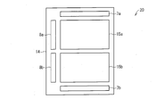
- FIG. 2 is a plan view schematically showing the overall configuration of the LCD 20.
- the LCD 20 includes a liquid crystal panel 14 (display screen), signal line drive circuits 7a and 7b, and scanning line drive circuits 8a and 8b.
- the liquid crystal panel 14 is divided into a display area 15a (first display area) and a display area 15b (second display area) which will be described later.
- display is performed by a reflection system or a transflective system
- display is performed by a transmission system or a transflective system.
- the liquid crystal panel 14 is configured by sandwiching a liquid crystal layer between a TFT substrate (not shown) and a counter substrate (not shown).
- a plurality of pixels 10a and 10b are arranged.
- the liquid crystal panel 14 includes a memory circuit 1, a pixel electrode 2, a signal line 3, a scanning line 4, and a thin film transistor (TFT) 13 on a TFT substrate. Further, a counter electrode 9 and counter electrode drive circuits 11a and 11b are provided on the counter substrate.
- Reference numeral 12 in the figure denotes a liquid crystal cell, and the liquid crystal cell 12 is electrically handled as a capacitive element.
- one signal line 3 is formed in each column so as to be parallel to each other in the column direction (vertical direction), and the scanning lines 4 are parallel to each other in the row direction (horizontal direction). Thus, one is formed in each row.
- the plurality of signal lines 3 and the plurality of scanning lines 4 are arranged so as to intersect with each other, and a pixel 10a is individually formed at each intersection. That is, a region surrounded by two adjacent signal lines 3 and two adjacent scanning lines 4 is one pixel 10a (first pixel).
- the memory circuit 1 and the pixel electrode 2 are formed corresponding to each pixel 10a.
- the memory circuit 1 includes a memory unit 6 that stores a data signal supplied from the signal line 3 and a display voltage supply circuit 5 that supplies the data signal stored in the memory unit 6 to the pixel electrode 2.
- FIG. 3 is an enlarged schematic view of the pixel 10a.
- the signal line 3 and the scanning line 4 are electrically connected to the memory circuit 1 and the display voltage supply circuit 5 arranged in each row, respectively.
- the signal line 3 and the scanning line 4 are electrically connected to the memory unit 6 in the memory circuit 1.
- a display voltage supply circuit 5 is electrically connected between the memory unit 6 and the pixel electrode 2.
- the pixel electrode 2 forms a liquid crystal capacitor with a counter electrode 9 through a liquid crystal cell 12.
- the data signal supplied from the signal line driving circuit 7a to the signal line 3 is temporarily written in the memory unit 6 by the scanning signal supplied from the scanning line driving circuit 8a to the scanning line 4.
- the data signal written in the memory unit 6 is written into the pixel electrode 2 via the display voltage supply circuit 5, and the pixel electrode 2 is set to a potential corresponding to the data signal.
- the counter electrode 9 is set to a predetermined potential by the counter electrode drive circuit 11a, and the liquid crystal cell 12 interposed between the pixel electrode 2 and the counter electrode 9 realizes gradation display according to the potential difference between the two electrodes. can do.
- the image display via the memory circuit 1 will be described in detail later.
- one signal line 3 is formed in each column so as to be parallel to each other in the column direction (vertical direction), and the scanning lines 4 are parallel to each other in the row direction (lateral direction).
- One is formed for each row.
- the plurality of signal lines 3 and the plurality of scanning lines 4 are arranged so as to cross each other, and a pixel 10b is individually formed at each intersection. That is, a region surrounded by two adjacent signal lines 3 and two adjacent scanning lines 4 is one pixel 10b (second pixel).
- the TFT 13 and the pixel electrode 2 are formed corresponding to each pixel 10b.
- a source electrode of the TFT 13 is electrically connected to the signal line 3, and a gate electrode is electrically connected to the scanning line 4. Further, the drain electrode is electrically connected to the pixel electrode 2.
- the pixel electrode 2 forms a liquid crystal capacitor with a counter electrode 9 through a liquid crystal cell 12.
- the gate of the TFT 13 is turned on by the scanning signal supplied from the scanning line driving circuit 8b to the scanning line 4, and the data signal supplied from the signal line driving circuit 7b to the signal line 3 is written into the pixel electrode 2 to write the pixel electrode.
- 2 is set to a potential corresponding to the data signal.
- the counter electrode 9 is set to a predetermined potential by the counter electrode drive circuit 11b, and the liquid crystal cell 12 interposed between the pixel electrode 2 and the counter electrode 9 has a gradation display corresponding to the potential difference between the two electrodes. Can be realized.
- the signal line 3 in the display area 15a is controlled by the signal line driving circuit 7a, and the scanning line 4 is controlled by the scanning line driving circuit 8a. Accordingly, the display area 15a is driven by the signal line driving circuit 7a and the scanning line driving circuit 8a.
- the signal line 3 in the display area 15b is controlled by the signal line driving circuit 7b, and the scanning line 4 is controlled by the scanning line driving circuit 8b. Accordingly, the display area 15b is driven by the signal line driving circuit 7b and the scanning line driving circuit 8b.
- the display area 15a and the display area 15b according to the present embodiment can be driven independently.
- the LCD 20 has the display area 15a and the display area 15b, and the memory circuit 1 is provided in each pixel 10a constituting the display area 15a.
- the memory circuit 1 will be described in detail.
- the memory circuit 1 is a circuit capable of storing image data such as still images. Therefore, by writing the image data stored in the memory circuit 1 to the pixel electrode 2, it is possible to display an image without supplying image data from the outside. That is, when the same image data is displayed in the display area 15a, the image can be displayed without continuously supplying the image data from the outside. Accordingly, it is not necessary to supply image data from the outside, and display can be performed with low power consumption. Specifically, after the image data is once written in the memory circuit 1, it is not necessary to charge / discharge the signal line 3 with the image data in order to supply the image data to each pixel 10a. Electric power can be reduced. Further, since it is not necessary to transmit image data from the outside of the liquid crystal panel 14 to the liquid crystal driver, it is possible to reduce power consumption associated with the transmission.
- a general memory circuit such as a pixel memory provided in a pixel may be used for the memory circuit 1 according to the present embodiment.
- the memory circuit 1 an SRAM type or a DRAM type has been developed.
- the memory circuit 1 that can be applied to this embodiment will be briefly described. As described above, the memory circuit 1 includes the memory unit 6 and the display voltage supply circuit 5. Since the memory circuit 1 can be a conventional memory circuit, its detailed internal configuration is not mentioned here. As the memory circuit 1, for example, a memory circuit disclosed in Japanese Patent Application Laid-Open No. 2007-286237 can be adopted, but is not particularly limited thereto.
- a data signal supplied from the signal line 3 is written in the memory unit 6 by supplying a high-level potential to the scanning line 4.
- the data signal written in the memory unit 6 is held by setting the potential of the scanning line 4 to a low level.
- the display voltage supply circuit 5 writes the data signal held in the memory unit 6 to the pixel electrode 2, and gradation display corresponding to the data signal is performed.
- the data signal stored in the memory circuit 1 can be written to the pixel electrode 2 of each pixel 10a. Therefore, when displaying the same image data such as a still image, the data signal stored in the memory circuit 1 may be supplied to each pixel 10a, and the data signal needs to be supplied to each pixel 10a for each frame. There is no. That is, since it is not necessary to drive the signal line driving circuit 7a and the scanning line driving circuit 8a, power consumption can be reduced.
- the image data stored (held) in the memory circuit 1 preferably has a relatively small amount of information and information update frequency.
- information update frequency is low, that is, if the frequency at which the images are switched is low, the same image data can be used continuously. Therefore, it is not necessary to supply new image data to the pixel 10a every time the image is switched (updated), and the power consumption can be further reduced.
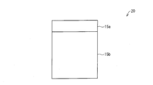
- FIG. 4 is a diagram illustrating an arrangement example of the display area 15a and the display area 15b.
- the size of the display area 15a and the display area 15b is not particularly limited, and can be set to a desired size.
- the LCD 20 includes the display area 15a and the display area 15b.
- One is a display area 15a that performs display by a reflective method or a semi-transmissive method
- the other is a display area 15b that performs display by a transmissive method or a semi-transmissive method.
- a reflective electrode that reflects external light is used as the pixel electrode 2.
- the pixel electrode 2 includes a portion configured by an electrode that transmits light from a backlight and a portion configured by an electrode that reflects external light.
- the transflective electrode is used.
- a transmission electrode that transmits light from the backlight is used as the pixel electrode 2.
- the pixel electrode 2 includes a portion configured by an electrode that transmits backlight light and a portion configured by an electrode that reflects external light. The transflective electrode is used.
- FIG. 5 is an enlarged schematic view showing the pixel 10b when the display region 15b adopts the transmission method.
- (B) in FIG. 5 is an enlarged schematic view of the pixel 10b in the case where the display region 15b adopts a transflective method.
- the transmission electrode 2 a is used as the pixel electrode 2.
- the drain electrode of the TFT 13 is configured to be electrically connected to the transmissive electrode 2a.
- the pixel electrode 2 includes a transmissive portion 2c formed of an electrode that transmits light from the backlight; A transflective electrode 2b having a reflective portion 2d made of an electrode that reflects external light is used.
- the drain electrode of the TFT 13 is configured to be electrically connected to the transmissive portion 2c and the reflective portion 2d, respectively. The same applies to the case where display is performed by the transflective method in the display area 15a.
- the display area 15a when the display area 15a is displayed by the reflection method, it is not necessary to provide a backlight in the display area 15a, so that power consumption can be further reduced. Also, when the display area 15a is displayed by the transflective method, the reflective method and the transmissive method can be used together, so that the backlight lighting time is reduced and the power consumption can be suppressed. Therefore, in addition to providing the memory circuit 1 in the display area 15a, it is possible to realize further reduction in power consumption by performing display by a reflection method or a transflective method.
- the transflective method also in the display area 15b, the lighting time of the backlight is reduced, so that the power consumption can be further reduced.
- the reflection method or the semi-transmission method as the display method of the LCD 20, further reduction in power consumption can be obtained.
- the LCD 20 described above is provided with signal line driving circuits 7a and 7b, scanning line driving circuits 8a and 8b, and counter electrode driving circuits 11a and 11b corresponding to the display area 15a and the display area 15b, respectively.
- the drive circuit corresponding to each display area 15a, 15b it can respond to the case where the number of pixels differs for each display area 15a, 15b.
- the driving method AC driving or DC driving
- FIG. 6 shows details of the LCD 20a when the signal line drive circuit 7b is omitted.
- FIG. 6 is an equivalent circuit diagram showing the overall electrical configuration of the LCD 20a.
- the display area 15a and the display area 15b can share (connect) the signal line 3.
- the signal line driving circuit 7b can be omitted, and the signal line driving circuit 7a can be shared by the display area 15a and the display area 15b. Therefore, the signal line drive circuit 7a controls the signal lines 3 in the display area 15a and the display area 15b.
- the signal line drive circuit 7b can be omitted by sharing the signal line 3 in the display area 15a and the display area 15b, so that an extra space can be reduced. Further, since the number of constituent members of the LCD 20a can be reduced, the manufacturing process can be simplified and the manufacturing cost can be kept low.
- FIG. 7 shows details of the LCD 20b when some of the signal lines 3 are shared by the display area 15a and the display area 15b.
- FIG. 7 is an equivalent circuit diagram showing the overall electrical configuration of the LCD 20b.
- the signal line drive circuit 7a In the display area 15a, the signal line 3 that is not shared with the display area 15b is also controlled by the signal line driving circuit 7a. On the other hand, in the display area 15b, the signal line 3 that is not shared with the display area 15a is controlled by the signal line driving circuit 7b. According to this, although it is necessary to provide the signal line drive circuit 7b, the scale of the signal line drive circuit 7b can be reduced.
- the counter electrode drive circuit 11a may be shared by the display area 15a and the display area 15b, and the counter electrode drive circuit 11b may be omitted.
- FIG. 8 shows details of the LCD 20c in which the counter electrode drive circuit 11b is omitted.
- FIG. 8 is an equivalent circuit diagram showing the overall electrical configuration of the LCD 20c.
- the counter electrode 9 of each pixel 10a in the display area 15a and the counter electrode 9 of each pixel 10b in the display area 15b may be controlled by one counter electrode driving circuit 11a.
- the counter electrode drive circuit 11a can be shared by the display area 15a and the display area 15b, it is not necessary to provide the counter electrode drive circuit 11b. Therefore, since the counter electrode 11b can be omitted, an extra space can be reduced. In addition, since the number of constituent members of the LCD 20c can be reduced, the manufacturing process can be simplified and the manufacturing cost can be kept low.
- each pixel 10a is temporarily DC-driven.
- the TFT 13 and the pixel electrode 2 are formed in each pixel 10a corresponding to each pixel 10a.
- a source electrode of the TFT 13 is electrically connected to the signal line 3, and a gate electrode is electrically connected to the scanning line 4.
- the drain electrode is electrically connected to the pixel electrode 2.
- the pixel electrode 2 forms a liquid crystal capacitor with a counter electrode 9 through a liquid crystal cell 12.
- Each storage capacitor line is capacitively coupled to the pixel electrode 2 disposed in each row, and forms a storage capacitor (auxiliary capacitor) with each pixel electrode 2.
- the display region 15a is driven by a direct current when displaying by the reflection method.
- the AC drive is changed to the DC drive for a short time, and then the drive of the display area 15a is stopped. That is, various drive circuits (the signal line drive circuit 7a, the scanning line drive circuit 8a, and the counter electrode drive circuit 11a) in the display area 15a are stopped.
- the display region 15a is driven by a direct current when displaying by the transflective method.
- the backlight is turned off while an image is displayed on the display area 15a. Since only the portion corresponding to the display area 15a of the backlight is turned off, it is necessary to separately provide a backlight for irradiating the display area 15a and a backlight for irradiating the display area 15b. As a result, a portion of the pixel 10a that is configured by an electrode that transmits light from the backlight is darkly displayed.
- driving of the display area 15a is stopped. That is, various drive circuits (the signal line drive circuit 7a, the scanning line drive circuit 8a, and the counter electrode drive circuit 11a) in the display area 15a are stopped.
- the liquid crystal capacitance and the auxiliary capacitance in the portion formed by the electrode that reflects the external light in the pixel 10a are charged with a certain polarity.
- the accumulated state is such that a direct current electric field is applied to the liquid crystal cell 12. Therefore, the display area 15a is burned.
- the contrast is weaker than before the drive is stopped, but the state where the image displayed immediately before the drive is stopped is maintained. In this way, an image can be displayed while driving is stopped.
- the image data is displayed in a state where the display area 15a is stopped using the burn-in phenomenon of the display area 15a. Can do.
- the image data in the display area 15a is not updated (or until the burn-in phenomenon is maintained), it is not necessary to drive various drive circuits, so that power consumption can be saved.
- information is displayed on the first display area by a reflection method or a semi-transmission method, and information is displayed on the second display area by a transmission method or a semi-transmission method. It is characterized by displaying.
- the reflection method when the first display area is displayed by the reflection method, it is not necessary to provide a backlight in the first display area, so that power consumption can be further reduced. Also, when the first display area is displayed by the transflective method, the reflective method and the transmissive method can be used together, so that the backlight lighting time is reduced and the power consumption can be suppressed. Therefore, in addition to providing a memory circuit in the first display region, it is possible to realize further reduction in power consumption by performing display by a reflective method or a transflective method.
- the backlight lighting time is reduced, so that the power consumption can be further reduced.
- the reflection method or the semi-transmission method as the display method of the liquid crystal display device according to the present invention, the power consumption can be further reduced.
- each of the first pixels includes, as the pixel electrode, an electrode configured to reflect light, or an electrode composed of a portion that reflects light and a portion that transmits light.
- Each of the second pixels includes, as the pixel electrode, an electrode that transmits light, or an electrode that includes a portion that reflects light and a portion that transmits light.
- the first pixel capable of performing display by the reflection method or the semi-transmission method is obtained, and the second pixel capable of performing display by the transmission method or the semi-transmission method is obtained.
- the plurality of signal lines included in the first display region and the plurality of signal lines included in the second display region are different from each other. .
- the first display area and the second display area can be driven independently. Therefore, it is possible to cope with the case where the number of signal lines constituting the first display area is different from the number of signal lines constituting the second display area.
- liquid crystal display device among the plurality of signal lines included in the first display region, one connected to any of the plurality of signal lines included in the second display region. It is characterized by at least one.
- the scale of a circuit for driving the signal lines in the first display area and the signal lines in the second display area can be reduced.
- the plurality of signal lines included in the first display area are connected to any one of the plurality of signal lines included in the second display area. It is a feature.
- the signal lines constituting each of the first display area and the second display area can be shared. Accordingly, it is not necessary to separately provide a circuit for driving the signal lines constituting the first display area and a circuit for driving the signal lines constituting the second display area, so that extra space is reduced. be able to.
- the amount of the information or the information that is updated less frequently is displayed in the first display region than the information displayed in the second display region. It is characterized by that.
- image data with a small amount of information can be stored in the memory circuit. Further, if the information update frequency is low, that is, if the frequency at which the images are switched is low, the same image data can be used continuously. Therefore, it is not necessary to supply new image data to the first pixel every time the image is switched (updated), and the power consumption can be further reduced.
- the liquid crystal display device of the present invention can be suitably used for electronic devices such as personal computers, mobile phones, portable information terminals, portable music players, and digital cameras.
Landscapes
- Physics & Mathematics (AREA)
- Chemical & Material Sciences (AREA)
- Crystallography & Structural Chemistry (AREA)
- Engineering & Computer Science (AREA)
- Nonlinear Science (AREA)
- General Physics & Mathematics (AREA)
- Theoretical Computer Science (AREA)
- Mathematical Physics (AREA)
- Computer Hardware Design (AREA)
- Optics & Photonics (AREA)
- Control Of Indicators Other Than Cathode Ray Tubes (AREA)
- Liquid Crystal Display Device Control (AREA)
- Liquid Crystal (AREA)
Abstract
Description
本発明の一実施形態について図面を参照して説明する。まず、本実施形態に係る液晶表示装置(LCD)の概要について、図1および図2を参照して説明する。図1は、LCD20の全体の電気的構成を示す等価回路図である。図2は、LCD20の全体構成を概略的に示す平面図である。
上述したように、本実施形態に係るLCD20は、表示領域15aおよび表示領域15bを有しており、表示領域15aを構成する各画素10aには、メモリ回路1が設けられている。当該メモリ回路1について、詳しく説明する。
本実施形態に係るLCD20では、上述したように、表示領域15aおよび表示領域15bを有している。一方は、反射方式または半透過方式によって表示を行う表示領域15aであり、他方は、透過方式または半透過方式によって表示を行う表示領域15bである。表示領域15aが反射方式によって表示を行う場合には、画素電極2として外光を反射する反射電極を用いる。一方、表示領域15aが半透過方式によって表示を行う場合には、画素電極2として、バックライトの光を透過する電極で構成された部分と、外光を反射する電極で構成された部分とを有する半透過電極を用いる。同様に、表示領域15bが透過方式によって表示を行う場合には、画素電極2としてバックライトの光を透過する透過電極を用いる。一方、表示領域15bが半透過方式によって表示を行う場合には、画素電極2として、バックライトの光を透過する電極で構成された部分と、外光を反射する電極で構成された部分とを有する半透過電極を用いる。
上述したLCD20では、表示領域15aおよび表示領域15bそれぞれに対応する信号線駆動回路7a,7b、走査線駆動回路8a,8b、および対向電極駆動回路11a,11bが設けられている。このように、それぞれの表示領域15a,15bに対応した駆動回路を設けることによって、表示領域15a,15bごとに画素数が異なる場合に対応することができる。また、表示領域15a,15bごとに駆動方法(AC駆動またはDC駆動)が異なる場合には、上記のように各表示領域15a,15bに対応した駆動回路を設けることが好ましい。
以上では、表示領域15aの各画素10aには、メモリ回路1を設ける構成を示したが、必ずしもこれに限定されるわけではない。例えば、各画素10aを一時的に直流駆動させる構成にすることも可能である。この場合は、各画素10aには、画素10bと同様に、各画素10aに対応してTFT13および画素電極2がそれぞれ形成されている。TFT13のソース電極が信号線3に電気的に接続されており、ゲート電極が走査線4に電気的に接続されている。また、ドレイン電極が画素電極2に電気的に接続されている。なお、画素電極2は、対向電極9との間に液晶セル12を介して液晶容量を形成している。また、各蓄積容量線は、それぞれ各行に配置された画素電極2と容量結合されており、各画素電極2との間で蓄積容量(補助容量)を形成している。
以上のように、本発明に係る液晶表示装置においては、上記第1表示領域に、反射方式または半透過方式によって情報を表示し、上記第2表示領域に、透過方式または半透過方式によって情報を表示することを特徴としている。
2 画素電極
2a 透過電極
2b 半透過電極
2c 透過部分
2d 反射部分
3 信号線
4 走査線
5 表示電圧供給回路
6 メモリ部
7a,7b,17 信号線駆動回路
8a,8b,18 走査線駆動回路
9 対向電極
10a,10b 画素
11a,11b 対向電極駆動回路
12 液晶セル
13 薄膜トランジスタ
14 液晶パネル
15a,15b 表示領域
20,20a,20b,20c,30 液晶表示装置
25a 反射領域
25b 反射・透過領域
Claims (7)
- 複数の走査線と、上記複数の走査線と交差する複数の信号線と、上記複数の走査線および上記複数の信号線の交差点ごとに個別に形成された複数の画素とを備えた表示画面を備え、
上記画素ごとに、画素電極と、上記画素電極に対向する対向電極と、上記画素電極と上記対向電極との間に配置された液晶層とを備えた液晶表示装置であって、
上記表示画面は、
上記複数の画素として、複数の第1画素を含んでいる第1表示領域と、
上記複数の画素として、上記複数の第1画素とは異なる複数の第2画素を含んでいる第2表示領域とに分割され、
上記第1画素ごとに、上記信号線から供給されるデータ信号を記憶するメモリ回路を備えていることを特徴とする液晶表示装置。 - 上記第1表示領域に、反射方式または半透過方式によって情報を表示し、
上記第2表示領域に、透過方式または半透過方式によって情報を表示することを特徴とする請求項1に記載の液晶表示装置。 - 上記第1画素ごとに、上記画素電極として、光を反射する電極、または光を反射する部分と光を透過する部分とから構成された電極を備え、
上記第2画素ごとに、上記画素電極として、光を透過する電極、または光を反射する部分と光を透過する部分とから構成された電極を備えていることを特徴とする請求項2に記載の液晶表示装置。 - 上記第1表示領域に含まれる上記複数の信号線と、上記第2表示領域に含まれる上記複数の信号線とは、それぞれ異なることを特徴とする請求項1~3のいずれか1項に記載の液晶表示装置。
- 上記第1表示領域に含まれる上記複数の信号線のうち、上記第2表示領域に含まれる上記複数の信号線のうちいずれかと繋がっているものが少なくとも1つあることを特徴とする請求項1~3のいずれか1項に記載の液晶表示装置。
- 上記第1表示領域に含まれる上記複数の信号線は、それぞれ上記第2表示領域に含まれる上記複数の信号線のうちいずれかと繋がっていることを特徴とする請求項5に記載の液晶表示装置。
- 上記第2表示領域に表示される情報と比較して、当該情報の量または当該情報の更新頻度が少ない上記情報を上記第1表示領域に表示することを特徴とする請求項1~6のいずれか1項に記載の液晶表示装置。
Priority Applications (5)
| Application Number | Priority Date | Filing Date | Title |
|---|---|---|---|
| SG2012072757A SG184373A1 (en) | 2010-04-02 | 2011-03-11 | Liquid crystal display device |
| CN201190000406XU CN202886781U (zh) | 2010-04-02 | 2011-03-11 | 液晶显示装置 |
| US13/638,083 US20130021231A1 (en) | 2010-04-02 | 2011-03-11 | Liquid crystal display device |
| AU2011236293A AU2011236293A1 (en) | 2010-04-02 | 2011-03-11 | Liquid crystal display device |
| JP2012509367A JPWO2011125416A1 (ja) | 2010-04-02 | 2011-03-11 | 液晶表示装置 |
Applications Claiming Priority (2)
| Application Number | Priority Date | Filing Date | Title |
|---|---|---|---|
| JP2010086444 | 2010-04-02 | ||
| JP2010-086444 | 2010-04-02 |
Publications (1)
| Publication Number | Publication Date |
|---|---|
| WO2011125416A1 true WO2011125416A1 (ja) | 2011-10-13 |
Family
ID=44762377
Family Applications (1)
| Application Number | Title | Priority Date | Filing Date |
|---|---|---|---|
| PCT/JP2011/055827 Ceased WO2011125416A1 (ja) | 2010-04-02 | 2011-03-11 | 液晶表示装置 |
Country Status (6)
| Country | Link |
|---|---|
| US (1) | US20130021231A1 (ja) |
| JP (1) | JPWO2011125416A1 (ja) |
| CN (1) | CN202886781U (ja) |
| AU (1) | AU2011236293A1 (ja) |
| SG (1) | SG184373A1 (ja) |
| WO (1) | WO2011125416A1 (ja) |
Cited By (1)
| Publication number | Priority date | Publication date | Assignee | Title |
|---|---|---|---|---|
| JP2021086097A (ja) * | 2019-11-29 | 2021-06-03 | シャープ株式会社 | 液晶表示パネル |
Families Citing this family (9)
| Publication number | Priority date | Publication date | Assignee | Title |
|---|---|---|---|---|
| JP2015125245A (ja) * | 2013-12-26 | 2015-07-06 | シナプティクス・ディスプレイ・デバイス合同会社 | 液晶表示装置、液晶ドライバ、及び、液晶表示パネルの駆動方法 |
| CN104992689B (zh) * | 2015-08-07 | 2017-12-08 | 京东方科技集团股份有限公司 | 阵列基板及其制作方法、显示装置及其驱动方法 |
| KR102471672B1 (ko) | 2015-11-13 | 2022-11-29 | 삼성전자주식회사 | 표시 제어 방법, 이를 구현한 디스플레이 패널, 디스플레이 장치 및 전자 장치 |
| CN110036434B (zh) * | 2016-12-08 | 2022-06-14 | 夏普株式会社 | 显示装置 |
| CN107195251B (zh) * | 2017-07-12 | 2018-03-13 | 深圳市华星光电半导体显示技术有限公司 | 一种阵列基板和显示面板 |
| US10319273B2 (en) | 2017-07-12 | 2019-06-11 | Shenzhen China Star Optoelectronics Semiconductor Display Technology Co., Ltd | Array substrates and display panels |
| JP2020154213A (ja) * | 2019-03-22 | 2020-09-24 | 株式会社ジャパンディスプレイ | 表示装置及び検出システム |
| US11397490B2 (en) | 2020-12-10 | 2022-07-26 | Sharp Kabushiki Kaisha | Liquid crystal display device and method for driving same |
| CN114627828B (zh) * | 2020-12-10 | 2023-07-11 | 夏普株式会社 | 液晶显示装置及其驱动方法 |
Citations (3)
| Publication number | Priority date | Publication date | Assignee | Title |
|---|---|---|---|---|
| JP2002303863A (ja) * | 2001-01-15 | 2002-10-18 | Toshiba Corp | 液晶表示装置 |
| JP2003216116A (ja) * | 2002-01-23 | 2003-07-30 | Sharp Corp | 表示装置およびその制御方法、ならびにそれを搭載した携帯情報機器 |
| JP2005148453A (ja) * | 2003-11-17 | 2005-06-09 | Toshiba Matsushita Display Technology Co Ltd | 液晶表示装置 |
Family Cites Families (1)
| Publication number | Priority date | Publication date | Assignee | Title |
|---|---|---|---|---|
| TW536689B (en) * | 2001-01-18 | 2003-06-11 | Sharp Kk | Display, portable device, and substrate |
-
2011
- 2011-03-11 WO PCT/JP2011/055827 patent/WO2011125416A1/ja not_active Ceased
- 2011-03-11 CN CN201190000406XU patent/CN202886781U/zh not_active Expired - Lifetime
- 2011-03-11 US US13/638,083 patent/US20130021231A1/en not_active Abandoned
- 2011-03-11 AU AU2011236293A patent/AU2011236293A1/en not_active Abandoned
- 2011-03-11 JP JP2012509367A patent/JPWO2011125416A1/ja active Pending
- 2011-03-11 SG SG2012072757A patent/SG184373A1/en unknown
Patent Citations (3)
| Publication number | Priority date | Publication date | Assignee | Title |
|---|---|---|---|---|
| JP2002303863A (ja) * | 2001-01-15 | 2002-10-18 | Toshiba Corp | 液晶表示装置 |
| JP2003216116A (ja) * | 2002-01-23 | 2003-07-30 | Sharp Corp | 表示装置およびその制御方法、ならびにそれを搭載した携帯情報機器 |
| JP2005148453A (ja) * | 2003-11-17 | 2005-06-09 | Toshiba Matsushita Display Technology Co Ltd | 液晶表示装置 |
Cited By (2)
| Publication number | Priority date | Publication date | Assignee | Title |
|---|---|---|---|---|
| JP2021086097A (ja) * | 2019-11-29 | 2021-06-03 | シャープ株式会社 | 液晶表示パネル |
| JP7393927B2 (ja) | 2019-11-29 | 2023-12-07 | シャープ株式会社 | 液晶表示パネル |
Also Published As
| Publication number | Publication date |
|---|---|
| SG184373A1 (en) | 2012-11-29 |
| JPWO2011125416A1 (ja) | 2013-07-08 |
| US20130021231A1 (en) | 2013-01-24 |
| CN202886781U (zh) | 2013-04-17 |
| AU2011236293A1 (en) | 2012-10-25 |
Similar Documents
| Publication | Publication Date | Title |
|---|---|---|
| WO2011125416A1 (ja) | 液晶表示装置 | |
| US7948461B2 (en) | Image display device | |
| TWI383361B (zh) | 驅動電路、液晶裝置、電子機器及液晶裝置之驅動方法 | |
| US10527893B2 (en) | Pixel array substrate structure, method of manufacturing pixel array substrate structure, display device, and electronic apparatus | |
| JP4241850B2 (ja) | 液晶装置、液晶装置の駆動方法、および電子機器 | |
| US8681163B2 (en) | Display device, control method of display device and electronic apparatus | |
| US8242997B2 (en) | Liquid crystal display panel and liquid crystal display device having the same | |
| US20130187962A1 (en) | Mixed Transmissive-Reflective-Transflective Liquid Crystal Display | |
| KR101082286B1 (ko) | 액정표시장치 및 그의 구동방법 | |
| TW200919432A (en) | Liquid crystal device and electronic apparatus | |
| US7755565B2 (en) | Dual type flat panel display device | |
| JP2012145926A (ja) | 画素構造、表示装置、及び、電子機器 | |
| JP2012088736A (ja) | 表示装置 | |
| US20080180452A1 (en) | Display device and driving method thereof | |
| KR100470843B1 (ko) | 액티브 매트릭스형 표시 장치 | |
| KR20070066041A (ko) | 반투과형 액정표시장치 및 이의 구동방법 | |
| JP2008033296A (ja) | 液晶装置、および電子機器 | |
| JP3711006B2 (ja) | 表示装置 | |
| KR101696480B1 (ko) | 액정표시장치 및 그 제조방법 |
Legal Events
| Date | Code | Title | Description |
|---|---|---|---|
| WWE | Wipo information: entry into national phase |
Ref document number: 201190000406.X Country of ref document: CN |
|
| 121 | Ep: the epo has been informed by wipo that ep was designated in this application |
Ref document number: 11765318 Country of ref document: EP Kind code of ref document: A1 |
|
| WWE | Wipo information: entry into national phase |
Ref document number: 2012509367 Country of ref document: JP |
|
| WWE | Wipo information: entry into national phase |
Ref document number: 13638083 Country of ref document: US |
|
| NENP | Non-entry into the national phase |
Ref country code: DE |
|
| ENP | Entry into the national phase |
Ref document number: 2011236293 Country of ref document: AU Date of ref document: 20110311 Kind code of ref document: A |
|
| 122 | Ep: pct application non-entry in european phase |
Ref document number: 11765318 Country of ref document: EP Kind code of ref document: A1 |